I NASA/ASEE SUMPIER FACULTY FELLOWSHIP PROGRAM … · Survey the theory on which the calculation is...
30
1988 I NASA/ASEE SUMPIER FACULTY FELLOWSHIP PROGRAM MARSHALL SPACE FLIGHT CENTER THE UNIVERSITY OF ALABAMA ELECTRON MOBILITY IN MERCURY CADMIUM TELLURIDE Prepared by: James D. Patterson Academic Rank: Professor and Head University and Department: Florida Institute of Technology Physics/Space Science NASA/MSFC: Laboratory: Division : Branch: NASA Colleague: Date : Contract No.: Space Science Low-Gravity Science Crystal Growth Sandor L. Lehoczky August 19, 1988 NGT 01-002-099 The University of Alabama XXII https://ntrs.nasa.gov/search.jsp?R=19890012377 2020-05-11T04:39:26+00:00Z
Transcript of I NASA/ASEE SUMPIER FACULTY FELLOWSHIP PROGRAM … · Survey the theory on which the calculation is...
1988 I
NASA/ASEE SUMPIER FACULTY FELLOWSHIP PROGRAM
MARSHALL SPACE FLIGHT CENTER THE UNIVERSITY OF ALABAMA
ELECTRON MOBILITY IN MERCURY CADMIUM TELLURIDE
Prepared by: James D. Patterson
Academic Rank: Professor and Head
University and Department: Florida Institute of Technology Physics/Space Science
NASA/MSFC: Laboratory: Division : Branch:
NASA Colleague:
Date :
Contract No.:
Space Science Low-Gravity Science Crystal Growth
Sandor L. Lehoczky
August 19, 1988
NGT 01-002-099 The University of Alabama
XXII
https://ntrs.nasa.gov/search.jsp?R=19890012377 2020-05-11T04:39:26+00:00Z

ELECTRON MOBILII'Y IN MERCURY CADMIUM TELLURIDE
James D. Patterson Professor and Head, Physics and Space Sciences
Florida Institute of Technology Melbourne, Florida 32901
ABSTRACT
A previously developed program, which includes all. electronic interactions thought to be important, does not correctly predict the value of electron mobility in mercury cadmium telluride particularly near room temperature. Part of the reason for this discrepancy is thought to be the way screening is handled. It seems likely that there are a number of contributors to errors in the calculation. The objective of this work is to survey the calculation, locate reasons for differences between experiment and calculation, and suggest improvements.
XXII-i

ACKNOWLEDGMENTS
The author wishes to thank the NASA/ASEE Summer Faculty Fellowship Program. Special thanks are due Dr. Mike Freeman, UA University Programs Co-Director and Ernestine Cothran, NASA MSFC Program Director.
Thanks are especially expressed to NASA Colleague Sandor L. Lehoczky and to Frank Szofran of the Space Science Laboratoy.
The author is grateful to Shirley A. Buford,, of the Crystal Growth Branch, for typing this manuscript.
Finally the author is grateful to the Administration of the Florida Institute of Technology for granting a leave of absence which allowed participation in this program.

1. Introduction
Many relevant properties of and references about Hg Cd Te have already been given (Patterson (1987), see also Ap&g#diff 1).
The calculation of the transport properties of narrow band gap semiconductors (of which mercury cadmium telluride is an important example) have met with considerable success (Lehoczky et al. (1982), Szymanska et al. (1978), and Chattopadhyay and Nag (1974)). Nevertheless it is not unusual to find calculations (near room temperature) differing from experiment by a factor of order two.
The original idea of this project was that inadequate treatment of screening was the cause of discrepancies between calculation and experiment. However, in a calculation as complex as the mobility of electrons in a narrow band gap semiconductor (see Appendices 2 and 3 ) even the accuracy of the present calculations whould have to be regarded as good (Lehoczky et al. (1980)).
An easy way to test the importance of screening is to run the present codes with different values of the screening constants. As we will see such calculations lead one to feel there is a limit to the accuracy with which the mobility can be evaluated, and certainly a limit to how much the accuracy can be improved by improving the screening.
XXII-1

2. Objectives
a. Determine the effect on the mobility of electrons in Pay particu- Hg - Cd Te of variations in relevant parameters.
lah 3ttgntion to screeriing parameters.
b. Survey the theory on which the calculation is based to try to pinpoint areas that can be improved.
XXII-2

3 . Calculations
We start by observing that in the approximation con- sidered, the effects of screening are determhed by the screening lengths. There exist reasons for considering other values of these lengths beside the conventional one (Patterson, (1987), appendices 3 and 5). Thus we are motivated to consider the results of calculations in which the screening length is varied for fixed values of the other parameters.
We also show how variations in screening affect the results for different values of the Cd concentration (x). All our results are based on a program of Dr. S.L. Lehoczky as rewritten by Ernestine Cothran. The program considers electron interaction effects due to longitudinal optic phonons, ionized impurities, holes, acoustic phonons, composi- tional disorder and neutral defects.
In what follows, we present our calculations in terms of hypotheses and calculational tests of the hypotheses.
XXII-3

HyDothesis
Although screening is important sizable changes in screening are not sufficient to get agreement with experiment.
is the mobility, all Fermi-Thomas wave and T is the
at T = 300K, l7 = 5.6 x 10 l4 cm-3 (the donor concentration) D
f '2 .742, E at T = 100K, f l p = 5.6 x 1014 cm-3
cu fE = .665,
This is further shown by Figs. la and lb where one sees that it is necessary (for3 the example shown) to use .05 of the nominal values fork,; in order to obtain near agreement with experiment.
XXII-4

I I
Y, II W
9 4 !2 9 0 c
I-
4
.. w
\
x il
V W I" CL. 7 k-
W
x
X N
X *
N z "! 2 Y
Y, I-
A
a l-
G L L
0 L
I
X X X UJ * N
X X I 1-5

Hwothesis
The mobility varies monotonically (very roughly linearly) as a function of inverse screening length (kTF) .
N 3 O h Z = 200 x 10 - ) Test at x= .183, T= 100K, K$, = 5.6 x (1 / exp d.S
1 .75 .5 .25 .2 .1 .05 .01
1 .866 .707 .5 .447 -316 .224 .1
322 , 205 303,233 281,266 252 , 603 245,053 225,358 209 , 803 183,437
141,582 138 , 157 138 , 469 142 , 453 150,344 169 , 076 212 , 629
2- 3 c m
(kkxpz 15 x 10 E ) 14 cm-3 at x= .183, T= 300K, f f p = 5.6 x 10
6:
1 1 35,160 18 , 529 .75 .866 32 , 677 17 , 113 .5 .707 29 , 956 16 , 184 .25 .5 26,606 15,641 .2 .447 25,777 15 , 908 .1 .316 23,693 16,902 .05 .224 22 , 138 20,452 .01 .1 19 , 602
XXII-6

Hypothesis
The more carriers, the more screening we should have. Thus, the more the calculation should depend on variations in the screening length. Three ways the number of carriers can be varied are by varying the Hg concentration, varying the temperature T or varying the donor concentration.
Tests (These imply the above hypothesis is naive.)
at T= 300K, OD= 5.6 x cm-3
14 cm-3 at x= .183, nD= 5.6 x io
3 at x= .183 T=3 00 k 17,= 5.6 cn7-
XXII-7

I Hypothesis
At a fixed temperature, changes due to screening are more This is shown clearly in the important for smaller band gaps.
Figs. 2a and 2b.
A simple expression for the energy gap as a function of temperature and x is given by Dornhaus and Nimtz (1983) who also list more accurate expressions. The expression is only supposed to be used for .135 5 x 5 .203. In the table below the energy gap is evaluated from a slightly better expression in the program.
-4 E = -.3 + 5 x io T +(i.gi - ~ ) x x in ev. 4
We find at T = 300K,
E = -.15 + 1.61~. g
If x is the value of x for which the energy gap vanishes, %e find for T = 100 that xo = .138.
2
For no= 5.6
x
.14
.15
.16
.17
.18
.19
.20
- E , ( e d
.085
.098
.llO
.123
.136
.149
.162
5
x 10 14 cm-3 and T = 300K
16 7.85~10 6.79 5.82 4.94 4.15 3.47 2.88
2 41,971 cm /vs 39,160 36,247 33,425 30,732 28,212 25,884
z 1 v fk, )
54 , 805 49,705 44,930 40,407 36,312 32 , 620 29 , 370
.766
.788
.807
.827
.846
.865
.881
I
---I------ 12 , 834 10,545 8,683 6,982 5,580 4,408 3 , 486
. 2 3 4
. 2 1 2
. 1 9 3
. 1 7 3
.154
.135
.119
XXII-8

b, Ii
X
4;. ,Y,
N . -3
\" X
q- 4 ' I I
In 7
0 " In "
m ! Z W H
X X I 1-9

4. Conclusions and Recommendations
a. Screening is important but it is not the whole answer. There are undoubtedly several small corrections.
b. In a calculation as complex as this one, see Figs. 3a and 3b and the appendices, the existing calculation (Lehoczky (1980), (1982)) is already good. See also Nag (1980) for comparison.
c. Small corrections and rewriting the code for a more modern computer are realistic goals for improvement. The program is presently implemented in basic for an HP 9845B and it runs rather slowly.
XXI I- 10

L
-. XXII-11
REFERENCES
Books
1.
2.
3.
4 .
5.
6.
7.
8.
9.
Frank J. Blatt, IIPhysics of Electronic Conduction in Solids", McGraw-Hill Book Company, New York, 1968.
R. Dornhaus and G. Nimtz, "The Properties and Applica- tions of the Hg Tracts in Moderft-8hysics Vol. 98, Springer-Verlag, Berlin, 1983 p 119-300.
CdxTe Alloy System" in Springer
Charles J. Joachain, "Quantum Collision Theory", North-Holland Publ. Co. Amsterdam, 1975.
C. Kittel, lVIntroduction to Solid State Physics1', John Wiley, 1986, 6th Edition.
Gerald D. Mahan, "Many-Particle Physics", Plenum, 1981.
B.R. Nag, IIElectron Transport in Compound Semi- conductor", Springer Series in Solid-state Sciences", Springer-Verlag, New York, 1980.
0. Madelung, "Int -0duction to Solid State Theoryu1, Springer-Verlag ( lerlin), 1978.
K. Seeger, 'ISemic mductor Physicst1, Springer-Verlag (Berlin) 1985, Th rd Editicm.
A.H. Wilson, "The Theory 01' Metals", Cambridqe U. Press, Cambridge, 1958.
Reports
1. S.L. Lehoczky, F.R. Szofran, and B.G. Martin, '#Advanced Methods for Preparation and Characterization of. Infrared Detector Materials, Part I", NASA CR-161598, July 5, 1980.
2. J.D. Patterson, IIImproving the Method of Crlculating Electronic Properties of Narrow Bandgap Semi- conductorst1, NASA CR-179213, 1987, Marshall Space Flight Center pp XXVII ff.
XXII-12

PaDers
1.
2.
3 .
4.
5.
6.
7.
8.
9.
10.
J.M. Berroir and M. Voos, "Electronic Properties of II-VI Compound Superlatticesll , in !!The Physics of the Two-Dimensional Electron Gast8, Plenum Press, New York, 1987 , D. Chattopadhyay and B.R. Nag, IIMobility of Electrons in Hgl-xCdxTell, J. Appl. Phys. 4 5 , 1463 (1974)
D. Chattopadhyay and H.J. Queisser, IIElectron Scattering by Ionized Impurities in Semiconductorst1, Rev. Modern Pysics 53, 745 (1981).
J.J. Dubowski, T. Dietl, W. Szymanska, and R.R. Galazka, "Electon Scattering in CdxHgl - xTelt, J. Phys, Chem. Solids 42, 351 (1981).
H. Ehrenreich, IIScreening Effects in Polar Semi- conductors", J. Phys. Chem. Solids 8 , 130 (1959)
K. Jozwikowski and A. Rogalski, IIIntrinsic Carrier Concentrations and Effective Masses in the Potential Infrared Detector Material Hgl-xZnxTe,ll Infrared Physics 28, 101 (1988).
Evan 0. Kane, "Band Structure of Indium Antimonide," J. Phys. Chem. Solids I, 249 (1957).
S.L. Lehoczky, J.G. Broerman, Donald A. Nelson, and Charles R. Whitsett, "Temperature-dependent electrical properties of HgSe", Phys. Rev. B 2, 1598 (1974).
S.L. Lehoczky, C.J. Summers, F.R. Szofran, and B.G. Martin, vtElectrical Characterization of Hg -x CdxTe Alloys1I, in Materials Processins in Reauced Gravity Environment of Space, Guy E. Rindone, Ed., Elsevier Science Publ. Co., Inc. Amsterdam, 1982.
D.A. Nelson, J.G. Broerman, C.J. Summers, and C.R. Whitsett, IIElecton Transport in the Hg CdxSe Alloy System!@, Phys. Rev. B 18, 1658 ($978) . ,
XXII-13

11. T.F. Rosenbaum, Stuart B. Field, D . A . Nelson, and P.B. Littlewood, "Magnetic-Field-Induced Localization Transition in HgCdTe", Phys. Rev. Lett. 54, 241 (1985).
12. W. Szymanska and T. Dietl, "Electron Scattering and Transport Phenomena in Small-Gap Zinc-Blende Semi- conductors", J. Phys. Chem =, 1025 (1978).
13. W. Szymanska, "Electron Scattering and Transport Phenomena in Narrow Gap Mercury Compounds and Alloyst1, Physics of Narrow Gap Semiconductor, Ed. by J. Rauluszkiowicz, M. Gorska, and E. Kaczmanek, pp 357- 379, Elsevier, Amsterdam, 1978.
14. W. Szymanska, "Electron Scattering and Classical Transport Phenomena in Small-Gap Semiconductors", Physics of Narrow Gap Semiconductors, Ed. by E. Gornik, H. Heirrich and L. Palmetshafer, Springer- Verlag, Berlin 19E2, p. 45.
15. W. Zawadzki, "Electron Transport Phenomena in Small-Gap Semiconductorsvf, Adv. Phys. 23, 435 (1974).
XXI I - 14

Appendix 1
Brief Properties of Hql,x Cd Te- .
1. zincblende.
Pseudo Binary 11-VI Compound with structure isomorphic to
2. The bandgap is tunable form 0 to 1.605 eV as x goes from about .17 (at low temperature) to 1.0. The bandgap also depends on temperature. Hg Cd Te forms a continuous range of solid solutions between tkxse%imetal HgTe and the semicon- ductor CdTe.
3 . Can use as an infrared detector at liquid nitrogen temperature in the wavelength range 8-12,& - an atmospheric window. A higher operating temperature than alternative materials, high detectivity, fast response, high sensitivity, IC compatible and low power.
4 . Candidate for microgravity crystal growth.
5. Band structure involves mixing of unperturbed valence and conduction band wave functions as derived by the Kane theory. Non parabolic bands.
6 . Typical carriers have small effective mass (about free electron mass) which implies large mobility. The effective mass also has a strong dependence on concentration and temperature.
7. Polar scattering by LO lattice vibration modes dominate above 77K (or so) and the relaxation time approximation is not valid. The scattering is inelastic since the phclnon energy is comparable to the electron energy.
8. Narrow bandgap semiconductors imply thermally excited electrons and hence screening. There may also be antiscreening effects when the phonons have higher phase velocity than the Fermi velocity of electrons.
Dornhaus and Nimtz (1983) list many more properties.
XXII-15
Appendix 2
Boltzmann Transport Equation and Solution
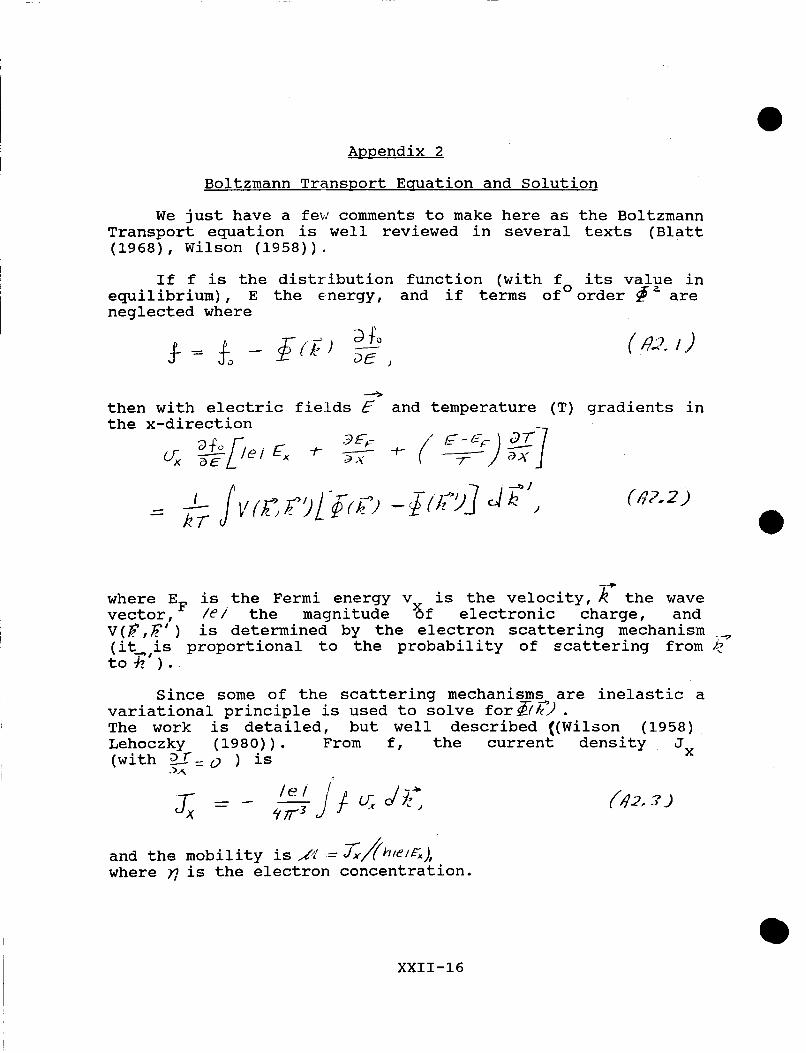
We just have a few comments to make here as the Boltzmann Transport equation is well reviewed in several texts (Blatt (1968) , Wilson (1958) ) .
If f is the distribution function (with fo its valye in equilibrium), E the energy, and if terms of order @ are neglected where
3 then with electric fields E and temperature (T) gradients in
---t
where EF is the Fermi energy v is the velocity, k the wave vector, / e / the magnitude '6f electronic charge, and V(F,F' ) is determined by the electron scattering mechanism .,l
(it_?,is proportional to the probability of scattering from e to* ) .
Since some of the scattering mechanisms are inelastic a variational principle is used to solve for&(h). The work is detailed, but well described ((Wilson (1958) Lehoczky (1980) ) . From f, the current density Jx (with Lr=, ) is
JJi
and the mobility is A'' = z / f b / t / & ) , where y? is the electron concentration.
XXI 1-1 6

Appendix 3
Electron Scatterins Mechanisms
The details here are too long to write down. Fortunately they have already been well described (Lehoczky (1980), Lehoczky (1974), Nelson (1978), Dubowski (19f21), Ehrenreich (1959), Zawadzki (1974), and Szymanska (1978)). Special mention should be made of Ehrenreich who wrote many of the key papers in this area. They are referenced in the above references.
a. Electon-phonon Interaction in Polar Solids
The only strong interactions are with longitudinal optic modes and we will limit discussion to long wave length modes near the center of the Brillouin zone with frequency&',. Several approximations then follow for which the literature may be consulted.
The a's are the phonon annihilation and creation operates and the C I S are the electron creation and annihilation operators. M is an apropriately chosen constant.
The screening is included by using tne dielectric function
and a tttwo modett theory is necessary (with frequencies close to those of CdTe and HgTe). is the high frequency dielectric constant.
XXII-17
. '

Further Comment Screenins and Antiscreeninq
Our main point here is to point out that antiscreening at small wave vectors can account for increased interaction and hence reduced scattering. This can occur when phonons with small wave vector also have high phase velocity which can occur for optical modes. As Ehrenreich (1959) has shown, the screened potential can actually be greater than the unscreened one.
b. Charsed Impurity and the Friedel Sum Rule
This is also referred to as ionized impurity scattering (ii):
with .Di;?/Fl being the periodic modulation of the plane wave in Blochls theorem and is often not included. V(q) is the Fourier transform of the Coulomb potential. Screening is included by E (9) and
where go is the low frequency dielectric constant. Screening was more fully discussed in the first report
(Patterson, 1987). Briefly, if a charge is placed in an electron gas its potential is better described by e-'y/r than / / r because the electrons in the gas surround the change and llscreenll it. The screening length is defined as A-' . The process is best described by a wave vector depen- dent dielectric constant, as above.
XXI I - 18

Further Comments: Multiple Scatterins and Other Corrections to Calculations
Chattopadhyay and Queisser (1981) have discussed cor- rections due to multiple scattering and impurity dressing. The usual assumption with regard to ionized impurity scatter- ing is that each impurity scatters independently. Multiple scattering adds corrections due to the electron interacting with more than one ion simultaneously. There is also a correction due to the fact that the impurities perturb the electron energies and wave functions. This is called the dressing correction and it can amount to 50% or so of the multiple scattering correction. However the corrections to ionized impurity scattering are not very importaqt compared to other scattering mechanisms in Hg Cd Te at temperatures of interest here. The dressing anh-%ul%iple scattering cor- rections to ionized impurity scattering are more important at higher temperatures and lower impurity concentrations.
Corrections to the Born approximation (in a calculation of ionized impurity scattering) can also be important at lower temperature but second order Born corrections are probably only useful if they are small.
An expression for the screening length L = h-'is given in appendix 5. It is possible to derive this directly or by use of the first Born approximation and the Friedel sum rule involving phase shifts 6~ (see e.g. Joachain, 1975). The Friedel sum rule holds generally and is supposed to be exact. It holds even for interacting electrons in a periodic sysem. The essential physical contents of the Friedel sum rule is the requirement of overall electrical neutrality about the charged ion. For electrons in a semiconductor, the Friedel sum rule takes the form, in the usual rotation;
C.
electron
Electron-Hole
(A36.Y)
When the heavy hole mass is large compared to the mass the hole can be considered to be stationarv
during scattering. This would make electron-hole scatterin; theory formally identical to ionized impurity scattering.
However we still must include non parabolity and admixture of p wave functions into the conduction band. For details see the references.
XXII-19

This is also a screened interaction. The following dielectric function has been used
d. Electron-Acoustic phonon
For semiconductors this is often treated by using the idea of a deformation potential (Seeger 1985, Madelung, 1978). If E, is the bottom of the conduction band then if E is the energy of the electron, we can obviously write
where ( € - E o ) is treated as the kinetic energy and Eo is viewed as the potential energy. One can think of €o varying with long wavelength displacements ( r) and this variation produces the deformation potential and thus the electron lattice coupling. At long wavelengths, Umklapp processes can be neglected. We write
3 for a single wave with wave vector . Further generaliza-
In the above V is the volume. tion leads to putting this in the us form (see references).
In the actual calculations, both longitudinal (L) and transverse (T) scattering is included by the use of three deformation potentials (lL, 2T).
e. Compositional Disorder and Neutral Defect Compositional Disorder
This is calculated by considering a random distribu- tion of scattering centers consisting of square wells.
XXII-20

The square wells are chosen to have a size equivalent to a unit cell and a depth (E ) determined by the differences in band gaps between CdTe an8 HgTe.
If Na is the number of unit cells per unit volume
(see Lehoczky et al., (1980)). The dependence on x(1-x) is known as Nordheim's rule. For a given x, x(1-x) measures the disorder assumed to be present (maximum) . Neutral Defect Scatterinq
This is also described as scattering by a random distri- bution of square-well potentials. It has been neglected in this calculation, but one assumes
(see Lehoczky et al:, (1980)), where N is the denslty of neutral defects, E is their strength and V is the volume of the cell.
XXII-21

Appendix 4
The Polaron Constant
The Polaron constant Y is defined, in the usual notation, as
o(= - 2ti k j i
It is a measure of the strength of the electron-lattice interaction and is dimensionless. For the phonon field and electrons to interact weakly we need 4 c1. For the Frohlich interaction term to be valid we also needx <1.
To get an estimate o f x we use the following values:
‘?(GO) = 15 I / e / = 4.8 x 10 -lo esu
I $ = 1.05 x 10 -27 erg-s 5 1 0 ) = 20
/n* = .03m I h-) = 9.1 x 10 gm -28
ergs -14 k d r = 2.4 x 10
Thus Q ( Z .092.
XXII-22

Band Structure and Effective Masses
We briefly summarize Kane (1957) theory here. We give some idea of the band structure near the top of the valence band and bottom of the conduction band. A simple schematic diagram of the band structure has been given by Seeger (1985), see also Lehoczky (1974). The s wave functions af the conduc- tion band are found to mix with the p wave functions of the valence band by T.7 perturbation theory (for F#d ) .
By using Bloch's theorem the wave function is given by
in the usual notation. The Schrodinger wave equation can be written :
where
M,
* and a V / Y ~
€ ' m
term has been neglected.
The Pauli operation is 2 .
To solve for the required energies, the eigenvalues of an 8 x 8 matrix must be determined.
XXII-23
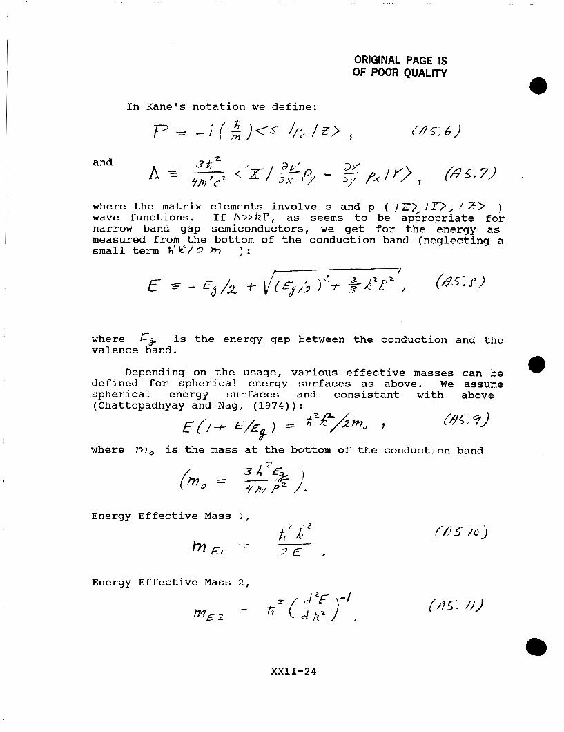
ORIGINAL PAGE IS OF POOR QUALfTY
and
In Kane's notation we define:
where the matrix elements involve s and p ( )X>, IT>, / z > ) wave functions. If A > > h P , as seems to be appropriate for narrow band gap semiconductors, we get for the energy as measured from the bottom of the conduction band (neglecting a small term hZkz/7- ) :
where E$ valence band.
is the energy gap between the conduction and the
Depending on the usage, various effective masses can be defined for spherical energy surfaces as above. We assume spherical energy su -faces and consistant with above (Chattopadhyay and Nag, (1974)):
(v5-, 7)
where D?* is the mass at the bottom of the conduction band 3
Energy Effective Mass
El
Energy Effective Mass
)?E z
3 xi-€- -% ) +CY P
2 ,
(14 -5'. / c j
XXII-24

Momentum Effective Mass,
4
( h,p ;p" = hg* It is relatively easy to show
and Lr and x7 are parallel).
all three of these agree at the bottom of the conduction band ( E=o, k = o ) -
Which one of these is appropriate depends on the usage.
The conventional effective mass as defined, for example, by Kittel (1986, p 194) is f i t g , ~ . The effective mass equation may be used as a starting point for discussing scattering in the Born approximation in solids. It would appear from a development of that equation (Madelung (1978), p. 79) that energy effective mass 1 could be the appropriate 2ffective mass to use. For HgCdTe, P+ is typically aboilt 10- of the mass of free electrons and has a strong dependence on carrier concentration and temperature.
By a standard development in the first Born approxima- tion, the screening length comes out (see e.g. Patterson (1987) 1 ,
However, for this result to be applicable to non parabolic energy bands, the effective mass should be the momentum effective mass so that the density of states ( f ( ~ ) ) properly enters via
XXII-25
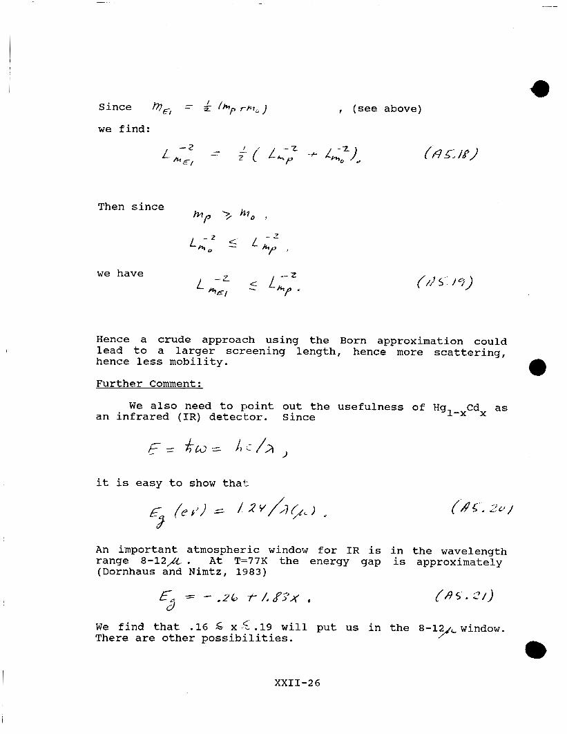
, (see above)
we have
Hence a crude approach using the Born approximation could lead to a larger screening length, hence more scattering, hence less mobility.
Further Comment:
We also need to point out the usefulness of Hgl-xCdx as an infrared (IR) detector. Since
it is easy to show that
An important atmospheric window for IR is in the wavelength range 8-12,LX. At T=77K the energy gap is approximately (Dornhaus and Nimtz, 1983)
( A 5 ' . 274
We find that .16 5 x 5 .19 will put us in the 8 - l y window. There are other possibilities.
XXII-26

Appendix 6
Miscellany
a. Wisner Lattice
In an electron gas in which the kinetic energy is much less important than the potential energy, a localization or ggcrystallizationtt of the electrons can occur. It appears that this phenomena actually occurs at x = .24 in Hg Cd Te at millikelvin temperature in a magnetic field (RosenkEm %t al. (1985) ) . b. Lavered Structures
One can make a superlattice consisting of alternating layers of CdTe and HgTe by use of molecular beam epitaxy. Such materials can be used as infrared detectors with proper- ties that may be superior to Hg Cd Te alloys (Berroir and Voos (1987) ) . 1-x x
As this report reflects, Hg Cd Te is the most important intrinsic semiconductor in&-a$edL detector material. Hg ZnxTe has been considered as a possible competitor, be&ffse it may be more structurally stable. The use of Hg Zn Te is still quj.te new and much effort is being devoted tol-'lry%tal growth techniques (Jozwikowski and Rogalski (1988) ) .
XXII-27


![[164] pinpoint](https://static.fdocuments.net/doc/165x107/587065dc1a28ab48378b4f79/164-pinpoint.jpg)