
I Ill11 Ill 11111 Ill11 111ll Ill11 Ill11 Ill11 111111 ... · I Ill11 llllllll Ill 11111 11111...
12
c I I l l 11 llllllll Ill 11111 11111 11111 Ill11 111 l l I l l 11 Ill11Ill11 111111 I l 1 1111 I l 1 US0065265~f-4Qf3-57-/ cL( (12) United States Patent (io) Patent No.: US 6,526,556 Bl Stoica et al. (45) Date of Patent: Feb. 25,2003 EVOLUTIONARY TECHNIQUE FOR AUTOMATED SYNTHESIS OF ELECTRONIC Stoica et al, ‘Toward On-Board Synthesis and Adaptation of Electronic Functions: an Evolvable Hardware Approach,” CIRCUITS IEEE, Mar. 1999, pp. 351-357.* Inventors: Assignee: Notice: Adrian Stoica, AItadena, CA (US); Carlos Harold Salazar-Lazaro, Pasadena, CA (US) The United States of America as represented by the Administrator of the National Aeronautics and Space Administration, Washington, DC (US) Subject to any disclaimer, the term of this patent is extended or adjusted under 35 U.S.C. 154(b) by 224 days. Appl. No.: 09/591,386 Filed Jun. 7, 2000 Related U.S. Application Data Continuation-in-part of application No. 09/395,235,filed on Sep. 13, 1999. Int. C1.’ ................................................ GMF 17/50 U S . C1. ............................... 716/16; 716/1; 716117; 706/13 Field of Search ................................ 716/16, 1‘7, 1; 706/13 References Cited U.S. PATENT DOCUMENTS 5,867,397 A 211999 Koze et al. ................. 3641489 5,897,628 A 411999 Kitano ........................ 706113 5,963,975 A * 1011999 Boyle et al. ................ 711/147 6,155,725 A * 122000 Scepanovic et al. ..... 395/500.1 OTHER PUBLICATIONS Adrian Stoica, “Toward Evolvable Hardware Chips: Experi- ments with a Programmable Transistor Array,” IEEE, Apr. 1999, pp. 1-7.* Zebulum et al, “Eiolvable Hardware: on the Automatic Synthesis of Analog Control Systems,” IEEE, Mar. 2000, pp. 451-463.* August0 et al, “Analog Fault Diagnostic in Nonlinear DC Circuits with an Evolutionaly Algorithm,” IEEE, Jul. 2000, pp. 609-616.* Stoica et al, “Evolution of Analog Circuits on Field Pro- grammable Transistor Arrays,” IEEE, Jul. 2000, pp. 1-lo.* Adrian Stoica, “Evolvable Hardware: From on-Chip Circuit Synthesis to Evolvable Space Systems,” IEEE, May 2000, Stoica et al, “Automatic Synthesis and Fault-Tolerant Experiments on an Evolvable Hardware Platform,” IEEE, Oct. 2000, pp. 465-471.* Stoica, “Reconfigurable Transistor Arrays for Evolvable Hardware,” NASA Tech Brief, vol. 25, No. 2, Item # from JPL New Technology Report NPO-20078, Jul. 26,1996, pp. i, 1, la-5a.* (List continued on next page.) pp. 1-9.* Primary Examiner-Vuthe Siek (74) Attorney, Agent, or Firm-John H. Kusmiss (57) ABSTRACT A method for evolving a circuit comprising configuring a plurality of transistors using a plurality of reconfigurable switches so that each of the plurality of transistors has a terminal coupled to a terminal of another of the plurality of transistors that is controllable by a single reconfigurable switch. The plurality of reconfigurable switches being con- trolled in response to a chromosome pattern. The plurality of reconfigurable switches may be controlled using an anneal- ing function. As such, the plurality of reconfigurable switches may be controlled by selecting qualitative values for the plurality of reconfigurable switches in response to the chromosomal pattern, selecting initial quantitative values for the selected qualitative values, and morphing the initial quantitative values. Qpically, subsequent quantitative val- ues will be selected more divergent than the initial quanti- tative values. The morphing process may continue to par- tially or to completely polarize the quantitative values. 35 Claims, 4 Drawing Sheets VAUNTION GOAL IS REACHED lTEF%TE UNTIL THE PERFORMANCE EVOLUTION https://ntrs.nasa.gov/search.jsp?R=20030053364 2018-06-26T04:48:06+00:00Z
Transcript of I Ill11 Ill 11111 Ill11 111ll Ill11 Ill11 Ill11 111111 ... · I Ill11 llllllll Ill 11111 11111...

c
I Ill11 llllllll Ill 11111 11111 11111 Ill11 111ll Ill11 Ill11 Ill11 111111 Ill1 1111 Ill1 US0065265~f-4Qf3-57-/ cL(
(12) United States Patent (io) Patent No.: US 6,526,556 B l Stoica et al. (45) Date of Patent: Feb. 25,2003
EVOLUTIONARY TECHNIQUE FOR AUTOMATED SYNTHESIS OF ELECTRONIC
Stoica et al, ‘Toward On-Board Synthesis and Adaptation of Electronic Functions: an Evolvable Hardware Approach,”
CIRCUITS IEEE, Mar. 1999, pp. 351-357.*
Inventors:
Assignee:
Notice:
Adrian Stoica, AItadena, CA (US); Carlos Harold Salazar-Lazaro, Pasadena, CA (US)
The United States of America as represented by the Administrator of the National Aeronautics and Space Administration, Washington, DC (US)
Subject to any disclaimer, the term of this patent is extended or adjusted under 35 U.S.C. 154(b) by 224 days.
Appl. No.: 09/591,386
Filed Jun. 7, 2000
Related U.S. Application Data
Continuation-in-part of application No. 09/395,235, filed on Sep. 13, 1999. Int. C1.’ ................................................ GMF 17/50 US. C1. ............................... 716/16; 716/1; 716117;
706/13 Field of Search ................................ 716/16, 1‘7, 1;
706/13
References Cited
U.S. PATENT DOCUMENTS
5,867,397 A 211999 Koze et al. ................. 3641489 5,897,628 A 411999 Kitano ........................ 706113 5,963,975 A * 1011999 Boyle et al. ................ 711/147 6,155,725 A * 122000 Scepanovic et al. ..... 395/500.1
OTHER PUBLICATIONS
Adrian Stoica, “Toward Evolvable Hardware Chips: Experi- ments with a Programmable Transistor Array,” IEEE, Apr. 1999, pp. 1-7.*
Zebulum et al, “Eiolvable Hardware: on the Automatic Synthesis of Analog Control Systems,” IEEE, Mar. 2000, pp. 451-463.* August0 et al, “Analog Fault Diagnostic in Nonlinear DC Circuits with an Evolutionaly Algorithm,” IEEE, Jul. 2000, pp. 609-616.* Stoica et al, “Evolution of Analog Circuits on Field Pro- grammable Transistor Arrays,” IEEE, Jul. 2000, pp. 1-lo.* Adrian Stoica, “Evolvable Hardware: From on-Chip Circuit Synthesis to Evolvable Space Systems,” IEEE, May 2000,
Stoica et al, “Automatic Synthesis and Fault-Tolerant Experiments on an Evolvable Hardware Platform,” IEEE, Oct. 2000, pp. 465-471.* Stoica, “Reconfigurable Transistor Arrays for Evolvable Hardware,” NASA Tech Brief, vol. 25, No. 2, Item # from JPL New Technology Report NPO-20078, Jul. 26,1996, pp. i, 1, la-5a.*
(List continued on next page.)
pp. 1-9.*
Primary Examiner-Vuthe Siek (74) Attorney, Agent, or Firm-John H. Kusmiss (57) ABSTRACT
A method for evolving a circuit comprising configuring a plurality of transistors using a plurality of reconfigurable switches so that each of the plurality of transistors has a terminal coupled to a terminal of another of the plurality of transistors that is controllable by a single reconfigurable switch. The plurality of reconfigurable switches being con- trolled in response to a chromosome pattern. The plurality of reconfigurable switches may be controlled using an anneal- ing function. As such, the plurality of reconfigurable switches may be controlled by selecting qualitative values for the plurality of reconfigurable switches in response to the chromosomal pattern, selecting initial quantitative values for the selected qualitative values, and morphing the initial quantitative values. Qpically, subsequent quantitative val- ues will be selected more divergent than the initial quanti- tative values. The morphing process may continue to par- tially or to completely polarize the quantitative values.
35 Claims, 4 Drawing Sheets
VAUNTION
GOAL IS REACHED lTEF%TE UNTIL THE PERFORMANCE
EVOLUTION
https://ntrs.nasa.gov/search.jsp?R=20030053364 2018-06-26T04:48:06+00:00Z

US 6,526,556 B1 Page 2
OTHER PUBLICATIONS
Bennett 111, F., Andre, D., Koza, J.R., and Keane, M.A., “Evolution of a 60 decibel Op Amp using genetic program- ming,” First International Conference, ICES96, Tsukuba, Japan, Oct. 7-8, 1996, Springer, pp. 455469. Flockton, Stuart, J., and Sheehan, Kevin, “Intrinsic Circuit Evolution Using Programmable Analogue Arrays,” Second International Conference, ZCES98, Lausanne, Switzerland, Sep. 23-25, 1998, Springer, pp. 144-153. Iba, H., Iwata, M. and Higuchi, T., “Machine Learning Approach to Gate-Level Evolvable Hardware,” First Inter- national Conference, ICES96, Tsukuba, Japan, Oct. 7-8, 1996, Springer, pp. 327-343. Kajitani, I., Hoshino, T., Nishikawa, D., Yokoi, H., Nakaya, S., Yamauchi, T., Inuo, T., Kajihara, N., Iwata, M., Keymeulen, D., Higuchi, T., “A Gate-Level Ettwchip: Implementing GA operations and Reconfigurable Hardware on a Single LSI,” Second International Conference, ICES98, Laussane, Switzerland, Sep. 23-25, Springer, pop. 1-12. Koza, J.R., Andre, D., Bennett III, F., Keane, M.A., “Reuse Parameterized Reuse, and Hierarchical Reuse of Substruc- tures in Evolving Electrical Circuits Using Genetic Pro- gramming, ”First International Conference, ICES96, Tsukuba, Japan, Oct. 7-8, 1996, Springer, pp. 312-325. Koza, J.R., Bennett In, F.H., Andre, D., Keane, M.A., “Automated WYWlWYG Design of Both the Topology and Component Values of Electrical Circuits Using Genetic Programming,” Proceedings of Genetic Programming Con- ference, Stanford, 1996, pp. 28-31. Koza, J.R., Dunlap, F., Bennett 111, E, Keane, M.A., Lohn, J., and Andre, D., “Automated Synthesis of Computational Circuits Using genetic Programming,” IEEE Transactions on Evolutionary Computation, vol. 1, No. 2, 1997, pp. 109-128.
Lohn, Jason D., and Colombano, S.P., “Automated Analog Circuit Synthesis Using a Linear Representation,” Second International Conference, ICES98, Lausanne, Switzerland, Sep. 23-25, Springer, 1998, pp. 125-133. Murakawa, M., Yoshizawa, S., Adachi, T., Suzuki, S., Taka- suka, K., Iwata, M., Higuchi, T., “Analogue EHW Chip for Intermediate Frequency Filters,” Second International Con- ference, ICES98, Lausanne, Switzerland, Sep. 23-25, 1998, Springer, pp. 132-143. Stoica, A., “On Hardware Evolvability and Levels of Granu- larity,” International Conference on Intelligent Systems and Semiotics, NIST Gaithersburg, VA, Sep. 1997, pp. 1-4. Thompson, Adrian, “Silicon Evolution,” Proceedings of Genetic Programming, MIT Press, 1996, pp. 75-90. Thompson, Adrian, “On the Automatic design of Robyst Electronics Through Artificial Evolution,” Second Interna- tional Conference, ICES98, Lausanne, Switzerland, Sep. 23-25, Springer, 1998, pp. 13-24. Thompson, Adrian, “An Evolved Circuit, Intrinsic in Sili- con, Entwined with Physics,” First International Confer- ence, ICES96, Tsukuba, Japan, Oct. 7-8, Springer, 1996, pp. 390405. Zebulum, R.S., Pacheco, M.A., Vellasco, M., ”Evolvable Systems in Hardware design: Taxonomy, Survey and Appli- cations,’’ First International Conference, ICES96, Tsukuba, Japan, Oct. 7-8, Springer, 1996, pp. 344-358. Zebulum, R.S., Pacheco. Marco, A., Vellasco, M., “Analog Circuits Evolution in Extrinsic and Intrinsic Modes,” Sec- ond International Conference, ICES98, Lausanne, Switzer- land, Sep. 23-25, Springer, 1998, pp. 154-165.
* cited by examiner

IJ.S. Patent Feb. 25,2003 Sheet 1 of 4
.
n z o c 3
W u
F: 3
US 6,526,556 B1

U.S. Patent Feb. 25,2003 Sheet 2 of 4
100
US 6,526,556 B l
70 I
315
I FIG. 2 20

1J.S. Patent Feb. 25,2003 Sheet 3 of 4 US 6,526,556 B l
J
L
0 r)
0 (v
0 F
a 0 0 = o 0 0
+ c u d
0 r)
0 rn
0 7
3 a 0 0 = o 0 0
0 M
0 N
0 v
a 0 0 = o 0 0
.3."0
0 M
0 (v
0 F
0

U.S. Patent Feb. 25,2003
I I I 1 I 1 I 1
t I I I I I I I I
I I
I I I I
-- I x4 --
-- --
RES ISTAN CE (Ohms)
. io9
104
Sheet 4 of 4 US 6,526,556 B1
LOW
10’ lo3 1 TEMPERATURE FACTOR
100
FIG. 4
1 .o
0.8
0.6
0.4
0.2
0
m= 1 4 7
L7
I I I
I x5 I I I I i
0
X6 FIG. 5

US 6,526,556 B1 1 ‘ 2
EVOLUTIONARY TECHNIQUE FOR AUTOMATED SYNTHESIS OF ELECTRONIC
CIRCUITS
in software simulations, specifically if one simulates large, complex analog circuits, and if the circuit response is rapid. Moreover, since the software simulation relies on models of
CROSS REFERENCE TO RELATED APPLICATIONS
physical hardware with limited accuracy, a solution evolved 5 in software may behave differently when downloaded in
programmable hardware; such mismatches are avoided This application is a continuation-in-part of U.S. appli- when evolution takes place directly in hardware. Further,
ser. N ~ . 09/395,235, by Adrian Stoics and carlOs unlike software evaluation where more complex circuitry S&zar-Lazaro, filed on Sep, 13, 1999, entitled EVOLU- and more accurate modeling takes longer to evaluate, hard- ~ O N A R Y TECHNIQUE FOR AUTOMATED s y m - 10 ware evolution scales well with both size of the circuits and SIS OF ELECTRONIC CIRCJITS, which is herein incor- model accuracy, thus providing less significant increases in porated by reference in its entirety. evaluation time.
Although reconfigurable devices exist, they have a limited BACKGROUND range of possible applications. On-chip evolution was dem-
Evolvable Hardware or E m is reconfigurable hardware l5 onstrated by A. Thompson, in Silicon Evolution, in Proceed- that self-configures under the control of an evolutionary ings of Genetic Programming 1996) (GP96) , MIT Press, ali;orithm. In evolutionary electronics, the search for an herein incorporated by reference in its entirety, using a Field electronic circuit reconfiguration can be made in software Or WGA as a Programmable and the final solution downloaded or become a blueprint for digital device, and a Genetic Algorithm Or GA as the hardware, which is referred to as extrinsic evolution. 2o Alternatively, evolution can be performed directly in Such a technique using gate arrays, however, is not hardware, referred to as intrinsic evolution. With intlinsic practical for analog circuit evolution. Logical gates are not evolution, solutions may be evolved directly on a chip. good elementary building blocks for analog circuits as they
The main steps of evolutionary synthesis are illustrated in 25 are designed optimized for logic&inW behaviors. For m(3. 1. First, a population of chromosomes is randomly example, transistor interconnections that are designed to generated. The chromosomes are converted into circuit facilitate digital logic signals and flows do not necessarily models for extrinsic EHW, or control bit strings downloaded Provide good analog response and signal flow. The usage of to programmable hardware for intrinsic E m . Circuit the gate array for evolution Can result in exploitation by responses are compared against specifications of a target evolution, of Parasitic and uninttmkd Signal Paths and response, and individuals are ranked based on how close 30 functioning modes for the components. AS a result, circuits they come to satisfying it. ~n preparation for a new iteration may evolve in one region of a chip that can not be replicated loop, a new population of individuals is generated from the in other Parts, Or on other Chips, although the Same genetic pool of best individuals in the previous generation, some of code is used. these individuals are taken as they were and some are 35 Moreover, conventional on chip evolution has not pro- modified by genetic operators such as chromosome cross- vided sufficient granularity for practical applications. While over and mutation. This process is repeated for many several levels of granularity are in use, the most common generations, and results in increasingly better individuals. digital devices are configurable at the gate-level. In the Such a process is usually stomed after a number of analog mogrammable devices. such as in Field Proeram-
Gate
mechanism.
- _ _ generations, or when the closeness to the target response has reached a sufficient degree. One of several solutions may be foLnd among the individuals of the last generation.
A variety of circuits have been synthesized through extrinsic evolutionary means. For example, Koza et al., in US. Pat. No. 5,867,397, issued on Feb. 2, 1999, entitled METHOD AND APPARATUS FOR AUTOMATED DESIGN OF COMPLEX STRUCTURES USING GENETIC PROGRAMMING, herein incorporated by ref- erence in its entirety, used Genetic Programming (GP) to grow an “embryonic” circuit to a circuit that satisfies desired requirements. This approach was used for evolving a variety of circuits, including filters and computational circuits. An alternative encoding technique using a linear representation, which has the advantage of reduced computational load, has been used in for automated filter design.
With these extrinsic approaches, though, evolutions of analog circuits were performed in simulations, without concern of a physical implementation, but rather, as a proof-of-concept that evolution can lead to designs that compete or even exceed the performance of human designs. Although in principle, one can test their validity in circuits built from discrete components, or in an ASIC, no analog programmable devices exist that would support the imple- mentation of the resulting design. Thus, these approaches do not provide a practical solution to intrinsic evolution.
Intrinsic evolution can speed-up the search for a solution circuit by a few orders of magnitude compared to evolution
4o mable-karog Arrays or PA&, the reconfigurable active elements are Operational Amplifiers, which have only very coarse granularity and little functionality with good precision, thus having only a limited range of possible applications.
Computation by analog circuitry has been lost as a technique for information processing because analog cir- cuits were not easily programmable, and required precise components with no drifts. If the evolutionary mechanism and process proves sufficiently powerful for evolving com-
50 plex analog circuits, then its combination with reconfig- urable analog devices potentially will be able to capture the benefits of analog in new applications. As such, the potential of analog processing is much greater than what is able to be exploited today.
Analog circuitry has advantages in cost, size and power consumption (as compared to digital circuitry) and can directly process signals that are continual in time and amplitude. Even a single transistor has many functions such as generation of square, square-root, exponential and loga-
60 rithmic functions, voltage-controlled current sources; analog multiplication of voltages, and short term and long term analog storage. As such, the basic combinations of transis- tors offer a rich repertoire of linear and nonlinear operators available for local and collective analog processing. Using
65 evolution, the benefits of analog processing can be exploited, while its disadvantages reduced or even elimi- nated.
45
55
US 6,526,556 B1 3 4
Also, it has been recognized by the inventors herein that evolutionary searches may perform significantly better with analog than with digital circuitry. A possible explanation lies in the fact that analog behaviors have relatively smoother spaces, which is better for the evolutionary search. Thus, 5 new perspectives are possible: evolutionary searches offer- ing automatic programming; sufficiently precise equivalent components could be obtained if the programmable analog components offer controllably of their operating points; and drifts that can be compensated for by adjusting operating I O points or, if the drifts are too strong, by a new search for a different optimal circuit configuration and operating point. Moreover, analog computation on simple low-power circuits can boost emerging applications areas of “smart matter” and
FIG. 5 shows parameter used for specification of a fitness function.
DESCRIPTION OF THE PREFERRED EMBODIMENTS AND METHODS OF THE
PRESENT INVENTION The preferred embodiment of the present invention pro-
vides a circuit adapted for use in intrinsic evolution. The preferred embodiment provides a programmable transistor array or PTA, which is programmable at the transistor level. In a preferred embodiment of the present invention, transis- tors form a plurality of modules, which may be intercon- nected to other modules, or to other transistors of the PTA, to provide further functionality.
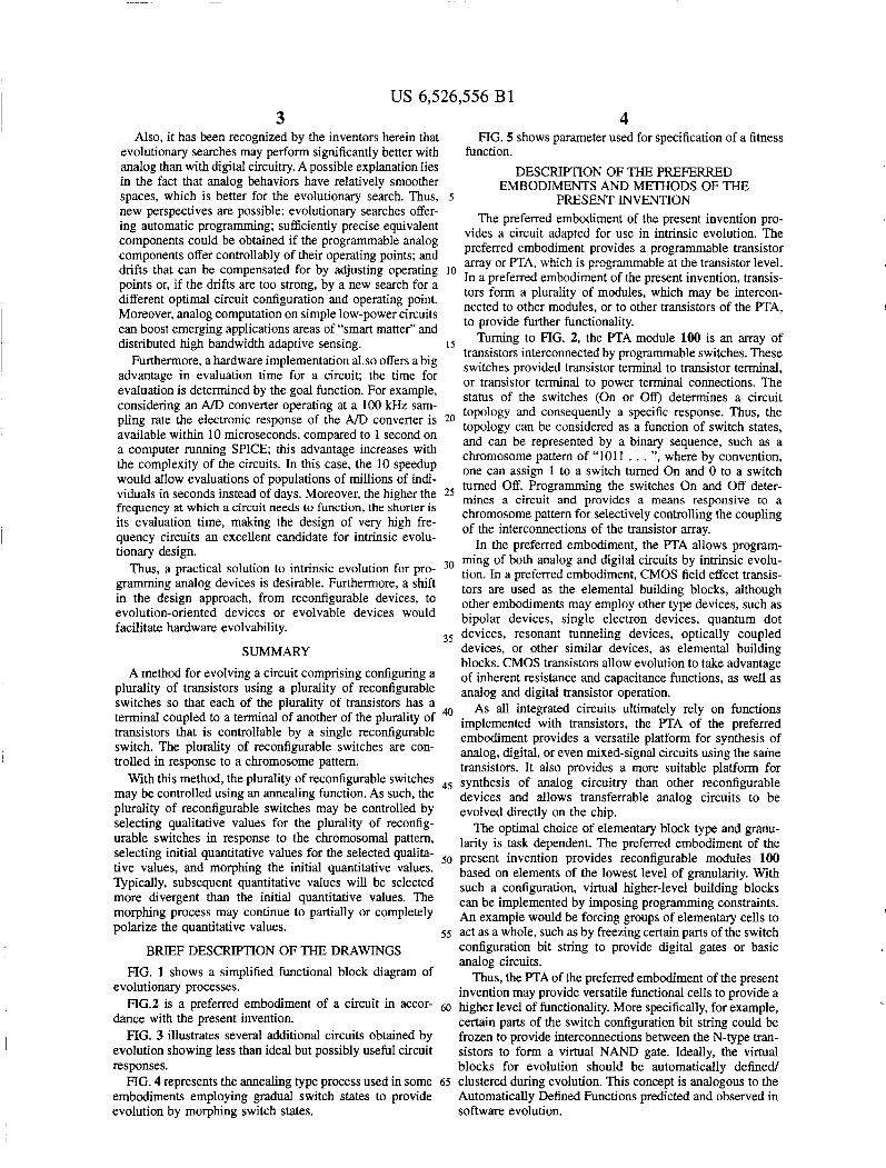
Turning to FIG. 2, the PTA module 100 is an array of transistors interconnected by programmable switches. These switches provided transistor terminal to transistor terminal, or transistor terminal to power terminal connections. The status of the switches (On or om determines a circuit
2o topology and consequently a specific response. Thus, the
and can be represented by a binary sequence, such as a chromosome pattern of . . . ,,, where by convention, one can assign to a switch turned off. Programming the switches On and Off deter-
responsive to a chromosome pattern for selectively controlling the coupling of the
In the preferred embodiment, the PTA allows program- 3o ming of both analog and digital circuits by intrinsic evolu-
tion. In a preferred embodiment, CMOS field effect transis-
distributed high bandwidth adaptive sensing. 15
Furthermore, a hardware implementation al.so offers a big advantage in evaluation time for a circuit; the time for evaluation is determined by the goal function. For example, ‘Onsidering an A/D converter Operating at a loo kHz
available within 10 microseconds, compared to 1 second on a computer running SPICE; this advantage increases with the complexity of the circuits. In this case, the 10 speedup would allow evaluations of populations of millions of indi- viduals in seconds instead of days. Moreover, the higher the 25 mines a circuit frequency at which a circuit needs to function, the shorter is its evaluation time, making the design of very high fre- quency circuits an excellent candidate for intrinsic evolu- tionary design.
Thus, a practical solution to intrinsic evolution for pro-
piing rate the response Of the A/D converter is topology can be considered as a function of switch states,
to a switch turned On and
provides a
of the transistor array.
gamming devices is Furthermore* a shift tors are used as the elemental building blocks, although in the design approach, from reconfigurable other embodiments may employ other type devices, such as to evolution-oriented devices or evolvable devices would facilitate hardware evolvability.
bipolar devices, single electron devices, quantum dot 35 devices, resonant tunneling devices, optically coupled
devices, or other similar devices, as elemental building blocks. CMOS transistors allow evolution to take advantage of inherent resistance and capacitance functions, as well as analog and digital transistor operation.
As all integrated circuits ultimately rely on functions
SUMMARY
A method for evolving a circuit comprising configuring a plurality of transistors using a plurality of reconfigurable switches so that each of the plurality of transistors has a terminal coup1ed to a Of another Of the Plurality Of t m h t o r s that is controllable by a sing1e reconfigurable
implemented with transistors, the PTA of the preferred embodiment provides a versatile platform for synthesis of
switch. The plurality of reconfigurable switches are con- analog, digital, or even mixed-signal circuits using the transistors. It also provides a more suitable platform for trolled in response to a chromosome pattern.
with this method, the Plurality ofreconfigurable switches 45 synthesis of analog circuitry than other reconfigurable may be controlled Using an annealing function. As such, the devices and allows transferrable analog circuits to be plurality of reconfigurable switches may be controlled by evolved directly on the chip. selecting qualitative values for the plurality of reconfig- choice of elementary block type and granu- urable switches in response to the Chrm~oSomal Pattern, larity is task dependent. The preferred embodiment of the selecting initial quantitative values for the selected qualita- 5o present invention provides reconfigurable modules 100
Typically, subsequent quantitative values will be selected higher-level building blocks
morphing process may Continue to Partially Or completely example would be forcing groups of elementary cells to polarize the quantitative values. 55 act as a whole, such as by freezing certain parts of the switch BRIEF DESCRIPTION OF THE DRAWINGS configuration bit string to provide digital gates or basic
ne
tive values, and morphing the initial quantitative values.
m r e divergent than the initial quantitative values. The
based on elements of the lowest level of granularity. With
can be implemented by imposing programming constraints. such a
FIG. 1 shows a simplified functional block diagram of evolutionary processes.
FIG.2 is a preferred embodiment of a circuit in accor- dance with the present invention.
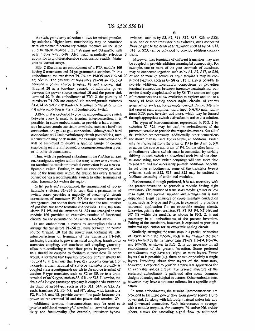
FIG. 3 illustrates several additional circuits obtained by evolution showing less than ideal but possibly useful circuit responses.
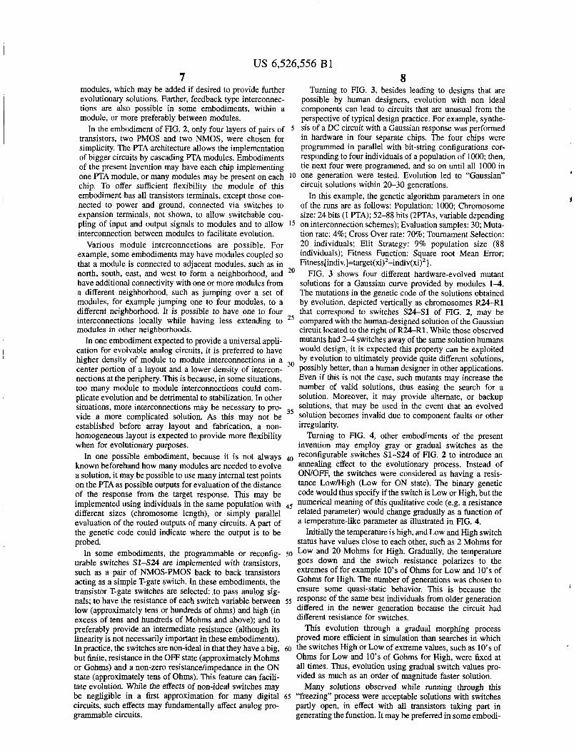
FIG. 4 represents the annealing type process used in some embodiments employing gradual switch states to provide evolution by morphing switch states.
analog circuits. Thus, the PTA of the preferred embodiment of the present
invention may provide versatile functional cells to provide a 60 higher level of functionality. More specifically, for example,
certain parts of the switch configuration bit string could be frozen to provide interconnections between the N-type tran- sistors to form a virtual NAND gate. Ideally, the virtual blocks for evolution should be automatically defined
65 clustered during evolution. This concept is analogous to the Automatically Defined Functions predicted and observed in software evolution.
1
a
US 6,526,556 B1 5 6
As such, granularity selection allows for mixed granular- ity solutions. Higher level functionality may be combined with elemental functionality within modules on the same chip to allow evolved circuit designs not obtainable with only higher level cells. Also, such granularity selection 5 tivity.
able in current arrays. be coupled to provide addition meaningful connectivity. For FIG. 2 illustrates an embodiment of a PTA module 100 example, one or more of the gate terminals of transistors
having 8 transistors and 24 programmable switches. In this may be connected together, such as by S1, S9, S17, or S24, embodiment, the transistors H-P4 are PMOS and N5-NS 10 or one or more of source or drain terminals may be con- arc: NMOS. The plurality of transistors Pl-N8 are coupled nected together, such as by SS or S1S. It also is possible to bei.ween a power source terminal 10 and a power sink provide additional meaningful connections by providing terminal 20 in a topology capable of admitting power terminal connections between transistor terminals not oth- beiween the power source terminal 10 and the power sink erwise directly coupled, such as by S6. The amount and type terminal 20. In the embodiment of FIG. 2, the plurality of 15 of interconnections allow evolution to explore and utilize a transistors PI-NS are coupled via reconfigurable switches variety of basic analog and/or digital circuits, of various SI -S24 so that every transistor terminal to transistor termi- granularities such as, for example, current mirror, differen- nal interconnection is via a reconfigurable switch. tial current pair, amplifier, multi-input NAND gate, multi-
4lthough it is preferred to provide a reconfigurable switch input XOR gate, inverter, and more, which may be formed between every terminal to terminal interconnection, it is 2o through appropriate switch activation, to arrive at a solution. possible, in some embodiments, to provide a hard comec- The types of interconnections represented in FIG. 2 by tioln between certain transistor terminals, such as a hard bias switches Sl-SU, may be used in embodiments of the connection, or a gate to gate connection. Although such hard present invention to provide the responsive means. Not all of connections will limit evolutionary circuit possibilities, such the switches are necessary. Additionally, other connections a cmnection may be desirable, for example, when evolution 25 not shown may be used. For example, an additional switch will be employed to evolve a specific family of circuits may be connected from the drain of P3 to the drain of NS, employing recurrent, frequent, or common connection types, or across the source and drain of P4. On the other hand, in or in other circumstances. embodiments where switch state is controlled by serially
‘nus, with the preferred embodiment, the PTAhas at least shifting to each switch to download each bit of the chro- one contiguous region within the m a y where every transis- 30 mosome string, more switch couplings will take more time tor tenninal to transistor terminal connection is via a recon- to program and not necessarily provide additional benefits. figurable switch. Further, in such an embodiment, at least In yet other embodiments, some of the transistor bypass one of the transistors within the region has every terminal switches, such as S12, S15, and S22 may be omitted to corlnected via a reconfigurable switch to other terminals of 35 facilitate cascading of additional modules. other transistor(s) within the region. Furthermore, although preferred, it is not necessary with
In the preferred embodiment, the arrangement of recon- the present invention, to provide a module having eight figurable switches Sl-S24 is such that a permutation of transistors. The number of transistors maybe greater or less switch states provides a majority of meaningful circuit than eight. The optimal number and arrangement is task connections of transistors Pl-N8 for a selected transistor 4o dependent. Eight transistors of complimentary conduction arrangement, but so that there are less than the total number types, such as N-type and P-type, is expected to provide a of possible transistor terminal connections. Thus, the tran- universal application for an evolvable analog circuit. sistors P1-NS and the switches Sl-S24 are arranged so that Likewise, pairing the transistors Pl-P2, P3-P4, NSN6, and module 100 provides an extensive number of functional N7-N8 within the module, as shown in FIG. 2, is not circuits for the permutation of switch S lS24 states. 45 necessary in all embodiments of the present invention. in one embodiment, a means to accomplish this is to Pairing Of the transistors, however, iS expected to provide a
arrange the transistors P1-NS in layers between the power universal application for an evolvable analog circuit. source terminal 10 and the power sink terminal 20. The Similarly, arranging the transistors in a particular number interconnections of terminals of the transistors Pl--NS, of layers within the module, such as for example the four including transistor to power tenninal coupling, transistor to 50 layers formed by the transistor pairs Pl-P2, P3-P4, N S N 6 , transistor coupling, and transistor self coupling generally and N7-NS, as shown in FIG. 2, is not necessary in all allow non-conflicting current flow paths. In general, termi- embodiments of the present invention. Some preferred nals should be coupled to facilitate current flow. In other embodiments may have six, eight, or more layers. Fewer words, a terminal that typically provides current should be layers also is possible (e.g. three or two or possibly a single coupled to at least one that typically receives current. For 55 layer). Providing about four layers of the transistors, example, a drain terminal of a P-type transistor typically is however, is expected to provide a universal application for cou,pled via a reconfigurable switch to the source terminal of an evolvable analog circuit. The layered structure of the anoi.her P-type transistor, such as S2 or S5, or to a drain preferred embodiment is patterned after some common terminal of an N-type, such as S3, S11, or S15. Likewise, the designs of analog and digital structures. Other embodiments, drain of a P-type transistor typically is coupled via switch to 60 however, may have a structure tailored for a specific appli- the drain of an N-type, such as SlO, S11, S14, or S15. As cation. such, transistor P1, P3, N5, and N7, along with transistors In some embodiments, the terminal interconnections are p2, €4, N6, and N8, provide current flow Paths between the provided to facilitate power flow from power source 1.0 to Power Source terminal 10 and the Power Sink terminal 20. power sink 20, along with left to right lateral and/or laterally
Additional terminal interconnections may be used to 65 and downward connection. Such interconnection strategy, provide additional meaningful terminal to terminal connec- with a module output at, for example, P4 andor N6, andor tivity and functionality (for example, transistor bypass others, allows for cascading signal flow to additional
switches, such as by S3, S7, S11, ,512, ,915, S20, or S22). Also, one or more transistor bias switches, ones connected from the gate to the drain of a transistor, such as by S4, S13, S16, or S23, can be provided to provide addition connec-
allows for hybrid digitallanalog solutions not readily obtain- Moreover, like terminals of different transistors may also
US 6,526,556 Bl 7 8
modules, which may be added if desired to provide further Turning to FIG. 3, besides leading to designs that are evolutionary solutions. Further, feedback type interconnec- possible by human designers, evolution with non ideal tions are also possible in some embodiments, within a components can lead to circuits that are unusual from the module, or more preferably between modules. perspective of typical design practice. For example, synthe- In the embodiment of FIG. 2, only four layers of pairs of 5 SiS Of a DC circuit with a Gaussian response was performed
transistors, two PMOS and two NMOS, were chosen for in hardware in four separate chips. The four Chips were simplicity. The PTA architecture allows the implementation Programed in Parallel With bit-stfing configurations Cor- of bigger circuits by cascading R A modules. Embodiments responding to four individuals Of a population of 1000; then, of the present invention may have each chip implementing tie next four were Programed, and SO on until all 1000 in one pTA module, or many modules may be present on each 10 one generation were tested. Evolution led to “Gaussian” chip. TO offer sufficient flexibility the module of this circuit SOlUtiOnS within 20-30 generations. embodiment has all transistors terminals, except those con- In this example, the genetic algorithm parameters in one nected to power and ground, connected via switches to of the runs are as follows: Population: 1000; Chromosome expansion terminals, not shown, to allow switchable cou- size: 24 bits (1 PTA); 52-88 bits (2PTAs, variable dcpending pling of input and output signals to modules and to allow 15 on interconnection schemes); Evaluation samples: 30; Muta- interconnection between modules to facilitate evolution. tion rate: 4%; Cross Over rate: 70%; Tournament Selection:
Various module interconnections are possible. For 20 individuals; Elit Strategy: 9% population size (88 example, some embodiments may have modules coupled SO individuals); Fitness Function: Square root Mean Error; that a module is connected to adjacent modules, such as in Fitness[indiv.l=target(xi)2-indiv(xi)2}. north, south, east, and west to form a neighborhood, and *O FIG. 3 shows four different hardware-evolved mutant have additional connectivity with one or more modules from solutions for a Gaussian curve provided by modules 14. a different neighborhood, such as jumping over a set of The mutations in the genetic code of the solutions obtained modules, for example jumping one to four modules, to a by evolution, depicted vertically as chromosomes R24-R1 different neighborhood. It is possible to have one to four that correspond to switches S W S 1 of FIG. 2, may be interconnections locally while having less extending to 25 compared with the human-designed solution of the Gaussian modules in other neighborhoods. circuit located to the right of W R 1 . While those observed In one embodiment expected to provide a universal appfi- mutants had 2-4 switches away of the same solution humans
cation for evolvable analog circuits, it is preferred to have would design, it is expected this Property Can be exploited higher density of module to module interconnections in a by evolution to ultimately provide quite different solutions, center portion of a layout and a lower density of intercon- 30 possibly better, than a human designer in other applications. nections at the periphery. This is because, in Some situations, Even if this is not the case, such mutants may increase the too many module to module interconnections could com- number of valid solutions, thus easing the search for a plicate evolution and be detrimental to stabilization. In other solution. Moreover, it may provide alternate, or backup situations, more intercoMections may be necessary to pro- solutions, that may be used in the event that an evolved vide a more complicated solution. As this may not be 35 solution becomes invalid due to component faults or other established before array layout and fabrication, a non- iEegUlaritY. homogeneous layout is expected to provide more flexibility Turning to FIG. 4, other embodiments of the present when for evolutionary purposes. invention may employ gray or gradual switches as the In one possible embodiment, because it is not always 4o reconfigurable switches s1-s24 Of FIG. 2 to introduce an
known beforehand how many modules are needed to evolve effect to the evolutionary Process. Instead of a solution, it may be possible to use many internal test points oN/oW, the switches were considered as having a resis- on the PTA as possible outputs for evaluation of the distance tance Lowmgh for ON state). The binary genetic of the response from the target response. This m y be Code would thus Specify if the switch is LOW or High, but the implemented using individuals in the Same population with 45 ~ U m e l k d ~eaI’liIlg Of this qUdhtiVe code (Cg. a resistance different sizes (chromosome length), or simply parallel related pameter ) would change gradually as a function of evaluation of the routed outputs of many circuits. A part of a temperature-like parameter as illustrated in FIG. 4. the genetic code could indicate where the output is to be Initially the temperature is high, and Low and High switch probed. status have values close to each other, such as 2 Mohms for
the tempramre urable switches S l S 2 4 are implemented with transistors, goes down and the switch resistance polarizes to the such as a of NMOS-PMOS back to back transistors extremes of for example 10’s of Ohms for Low and 10’s of acting as a simple T-gate switch. In these embodiments, the for High- The number Of generations was chosen to transistor T-gate switches are selected: to pass analog sig- ensure some quasi-static behavior. This is because the rials; to have the resistance of each switch variable between 55 response of the same best individuals from older generation low (approximately tens or hundreds of ohms) and high (in differed in the newer generation because the circuit had excess of tens and hundreds of Mohms and above); and to different resistance for switches. preferably provide an intermediate resistance (although its This evolution through a gradual morphing process linearity is not necessarily important in these embodiments). proved more efficient in simulation than searches in which In practice, the switches are non-ideal in that they have a big, 60 the switches High or LOW of extreme values, such as 10’s of but finite, resistance in the OFF state (approximately Mohms Ohms for Low and 10’s of Gohms for High, were fixed at or Gohms) and a non-zero resistancdimpedance in the ON all times. Thus, evolution using gradual switch values pro- state (approximately tern of Ohms). This feature can facfi- vided as much as an order of magnitude faster solution. tate evolution. While the effects of non-ideal switches may Many solutions observed while running through this be negligible in a first approximation for many digital 65 “freezing” process were acceptable solutions with switches circuits, such effects may fundamentally atfect analog pro- partly open, in effect with all transistors taking part in grammable circuits. generating the function. It may be preferred in some embodi-
In some embodiments, the programmable or reconfig- 50 and 2o Mohms for High.
i
1

.
US 6,526,556 B1 9 10
ments to allow the annealing process to continue until the switch states are frozen or polarized to their full high and low impedance states. This provides more robust solutions, ones that are not as sensitive to thermal changes of transistors, or to other transistor dependent variations. In 5 pattern; other embodiments, the switches may not be completely polarized. In such embodiments, the annealing process may be shortened, or not used at all, to provide solutions having switch states not completely polarized to their full high and low impedance states. Such solutions may be more desirable 1o response to morphed in certain instances, such as, for example, where design speed, resources, functionality, or other constraints make such solutions desirable. values.
[n such situations where design speed is an important factor, it is possible to provide a fitness function which includes fitness gradient information to characterize the likelihood of success of individual during the morphing process. As such, individuals not showing sufficient improvement in fitness during the morphing process could be abandoned to expedite the evolution process.
tance of the switches so provide a for variably controlling transistor coupling. The gradual switch may be
PMOS back to back transistors acting as a simple T-gate 25 switch. The switches are selected as discussed above. In the implementation of one embodiment, the meaning of high or low is controlled by an A/D converter, either externid or internal to the chip. h such an embodiment, a single bit of the bit string may be represented by several bits to provide 3o plurality of reconfigurable switches. adjustment of the value of high and low. Thus, a single bit 13. claim 2 wherein controlling the plurality of reconfig- used to qualitatively represent high or low is delivered to the urable switches comprises heterogenously controlling the A/[) converter, which in turn provides a quantitative analog plurality of reconfigurable switches. value of the higMow states to control the annealing process.
resistance value assigned the switches to represent high and low are controlled together to provide homogeneous control of higMow values of the switches. It also is possible in some embodiments to provide heterogeneous control of the switch annealing process to provide non-uniform, or even indi- 4o vidiial control of the values representing high and low.
A fitness function which considers shape information by using a weighted combination of parameters xl-x7 as depicted in FIG. 5 also can improve evolution search effi- cienicy over a Euclidian type fitness function in some appli- 45 cations. Fitness functions, such as the one of FIG. 5 used lo
3. claim 2 wherein controlling the plurality of reconfig-
a) selecting qualitative values for the plurality of recon- figurable switches in response to the chromosomal
b) selecting initial quantitative values for the selected
c) morphing the initial quantitative 4. claim 3 further
5. claim 4 wherein morphing comprises
urable switches comprises:
qualitative values; and
evaluating circuit fitness in
divergent than the initial quantitative
6. claim 5 wherein morphing comprises completely polar- izing the qualitative values.
7. claim 5 wherein morphing comprises partially polar- izing the qualitative values.
8. claim 5 wherein selecting initial quantitative values for the qualitative values comprises selecting quantitative val- ues within two orders of magnitude.
9. claim 8 wherein selecting initial quantitative values for the qualitative values comprises selecting quantitative val- ues within an Order Of magnitude.
polarizing the qualitative values.
values,
titative values
Gradual switches allow variable control over the resis- 2o
implemented with transistors, such as a pair of NMOS- lo. wherein morphing comprises completely
ll. claim wherein morphing number of generations to
providing a a gradual change
wherein controlling the plurality of reconfig- homogeneously controlling the
in circuit response. 12. claim
urable switches
14. A method for evolving a circuit comprising: a) coupling a plurality of transistors with a plurality of
reconfigurable switches so that each of the plurality of transistors within a region of the circuit is coupled via a single reconfigurable switch to a terminal of another of the plurality of transistors; and
b) controlling the plurality of reconfigurable switches in response to a chromosome pattern.
15. claim 14 wherein controlling the plurality of recon- figurable switches further comprises using an annealing function.
16. claim 15 wherein controlling the plurality of recon- figurable switches comprises:
I n one embodiment, to simplify device fabrication, the 35
evoive a Gaussian response circuit, however, generally do not have broad applicability.
While the preferred embodiments and methods of the present invention have been described in detail above, many changes to these embodiments and methods may be made without departing from the true scope and teachings of the present invention. The present invention, therefore, is lim- ited only as claimed below and the equivalents thereof.
We claim is: 1. A method for evolving a circuit comprising: a) configuring a plurality of transistors using a plurality of
reconfigurable switches so that each of the plurality of transistors has a terminal coupled to a terminal of another of the plurality of transistors such that a single reconfigurable switch controls respective couplings therebetween; and
b) controlling the plurality of reconfigurable switches in response to a chromosome pattern.
2. claim 1 wherein controlling the plurality of reconfig- urable switches further comprises using an annealing func- tion.
a) selecting qualitative values for the plurality of recon- figurable switches in response to the chromosomal pattern;
b) selecting initial quantitative values for the selected qualitative values; and
c) morphing the initial quantitative values. 17. claim 16 further comprising evaluating circuit fitness
in response to morphed quantitative values. 18. claim 17 wherein morphing comprises selecting quan-
titative values more divergent than the initial quantitative values.
19. claim 18 wherein morphing comprises completely polarizing the qualitative values.
20. claim 18 wherein morphing comprises partially polar- izing the qualitative values.
21. claim 18 wherein selecting initial quantitative values for the qualitative values comprises selecting quantitative values within two orders of magnitude.
22. claim 21 wherein selecting initial quantitative values for the qualitative values comprises selecting quantitative values within an order of magnitude.
50
55
60
65

US 6,526,556 B1 11 12
23. claim 22 wherein morphing comprises completely polarizing the qualitative values.
24. claim 18 wherein morphing comprises providing a sufficient number of generations to ensure a gradual change in circuit response.
25. claim 15 wherein controlling the plurality of recon- figurable switches comprises homogeneously controlling the plurality of reconfigurable switches.
26. claim 15 wherein controlling the plurality of recon- figurable switches comprises heterogenously controlling the io plurality of reconfigurable switches.
e) evaluating a fitness of the circuit in response to mor- phed quantitative values of the chromosomal pattern.
28. claim 27 wherein morphing comprises completely polarizing the qualitative values.
29. claim 27 wherein morphing comprises partially polar- izing the qualitative vah~es.
30. claim 27 wherein Selecting initial quantitative values for the qualitative values comprises selecting quantitative values Within two orders of magnitude.
31. claim 30 wherein Selecting initial quantitative values for the qualitative values comprises selecting quantitative values within an order of magnitude.
polarizing the qualitative values.
sufficient number of generatiomto ensure a gradual change in circuit response.
34. claim 27 wherein controlling the plurality of recon- figurable switches comprises homogeneously controlling the
35. claim 27 wherein controlling the reconfigurable switches comprises heterogenously controlling the plurality of reconfigurable switches.
5
27. A method for evolving a circuit comprising: a) configuring a plurality of transiston between a power 32. 31 wherein morphing comprises
source and a power sink with a plurality of reconfig-
each of the plurality of transistors within a region of the circuit are coupled via a single reconfigurable switch to a terminal of another of the plurality of transistors;
figurable switches in response to a chromosomal pat- tern;
c) selecting initial quantitative Values for the selected qualitative values;
urable switches so that each of at least two t e d n a l s of 15 33. 27 wherein morphing comprises providing a
b) selecting qualitative values for the plurality of recon- 2o plurality of reconfigurable switches.
d) morphing the initial quantitative values; and * * * * *


![111111 lllll11111111111 lllll1111111111111ll Ill11 Ill11111111 lllll11111111111 lllll1111111111111ll Ill11 111ll Ill11 1ll11l111 IIIII Ill1 US005194873A United States Patent [19] [ill](https://static.fdocuments.net/doc/165x107/5eb704680102e22d890d7b12/111111-lllll11111111111-lllll1111111111111ll-ill11-ill11-111111-lllll11111111111.jpg)