I. Blocking vs. Nonblocking Assignmentscourses.csail.mit.edu/6.111/f2007/handouts/L06.pdf · 6.111...
24
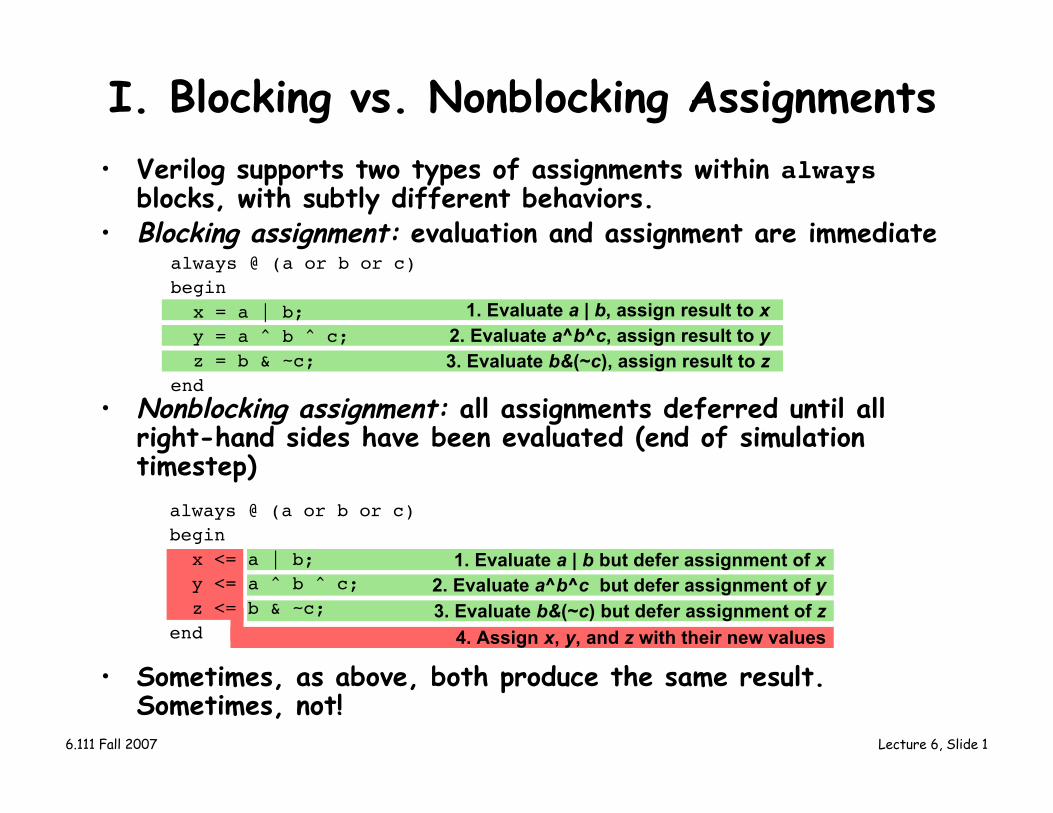
6.111 Fall 2007 Lecture 6, Slide 1 1. Evaluate a | b but defer assignment of x 2. Evaluate a^b^c but defer assignment of y 3. Evaluate b&(~c) but defer assignment of z 1. Evaluate a | b, assign result to x 2. Evaluate a^b^c, assign result to y 3. Evaluate b&(~c), assign result to z I. Blocking vs. Nonblocking Assignments • Verilog supports two types of assignments within always blocks, with subtly different behaviors. • Blocking assignment: evaluation and assignment are immediate • Nonblocking assignment: all assignments deferred until all right-hand sides have been evaluated (end of simulation timestep) • Sometimes, as above, both produce the same result. Sometimes, not! always @ (a or b or c) begin x = a | b; y = a ^ b ^ c; z = b & ~c; end always @ (a or b or c) begin x <= a | b; y <= a ^ b ^ c; z <= b & ~c; end 4. Assign x, y, and z with their new values
Transcript of I. Blocking vs. Nonblocking Assignmentscourses.csail.mit.edu/6.111/f2007/handouts/L06.pdf · 6.111...
6.111 Fall 2007 Lecture 6, Slide 1
1. Evaluate a | b but defer assignment of x2. Evaluate a^b^c but defer assignment of y3. Evaluate b&(~c) but defer assignment of z
1. Evaluate a | b, assign result to x 2. Evaluate a^b^c, assign result to y 3. Evaluate b&(~c), assign result to z
I. Blocking vs. Nonblocking Assignments• Verilog supports two types of assignments within always
blocks, with subtly different behaviors.• Blocking assignment: evaluation and assignment are immediate
• Nonblocking assignment: all assignments deferred until allright-hand sides have been evaluated (end of simulationtimestep)
• Sometimes, as above, both produce the same result.Sometimes, not!
always @ (a or b or c)begin x = a | b; y = a ^ b ^ c; z = b & ~c;end
always @ (a or b or c)begin x <= a | b; y <= a ^ b ^ c; z <= b & ~c;end 4. Assign x, y, and z with their new values
6.111 Fall 2007 Lecture 6, Slide 2
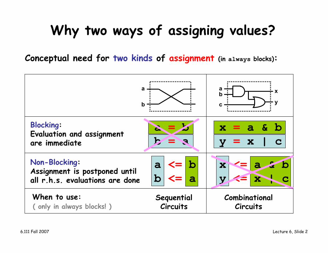
Why two ways of assigning values?
Conceptual need for two kinds of assignment (in always blocks):
ab
c
x
y
a
b
a = bb = a
x = a & by = x | c
Blocking:Evaluation and assignmentare immediate
a <= bb <= a
x <= a & by <= x | c
Non-Blocking:Assignment is postponed untilall r.h.s. evaluations are done
When to use: SequentialCircuits
CombinationalCircuits( only in always blocks! )
6.111 Fall 2007 Lecture 6, Slide 3
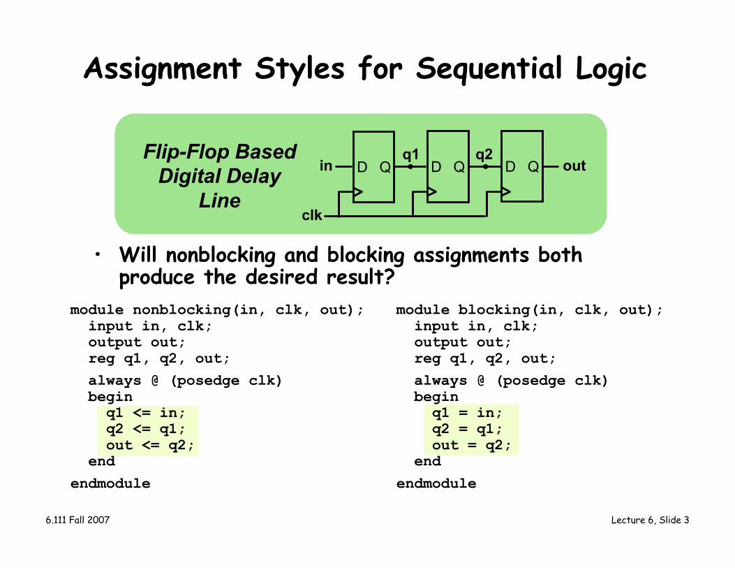
Assignment Styles for Sequential Logic
• Will nonblocking and blocking assignments bothproduce the desired result?
module nonblocking(in, clk, out); input in, clk; output out; reg q1, q2, out; always @ (posedge clk) begin q1 <= in; q2 <= q1; out <= q2; endendmodule
D Q D Q D Qin outq1 q2
clk
Flip-Flop BasedDigital Delay
Line
module blocking(in, clk, out); input in, clk; output out; reg q1, q2, out; always @ (posedge clk) begin q1 = in; q2 = q1; out = q2; endendmodule
6.111 Fall 2007 Lecture 6, Slide 4
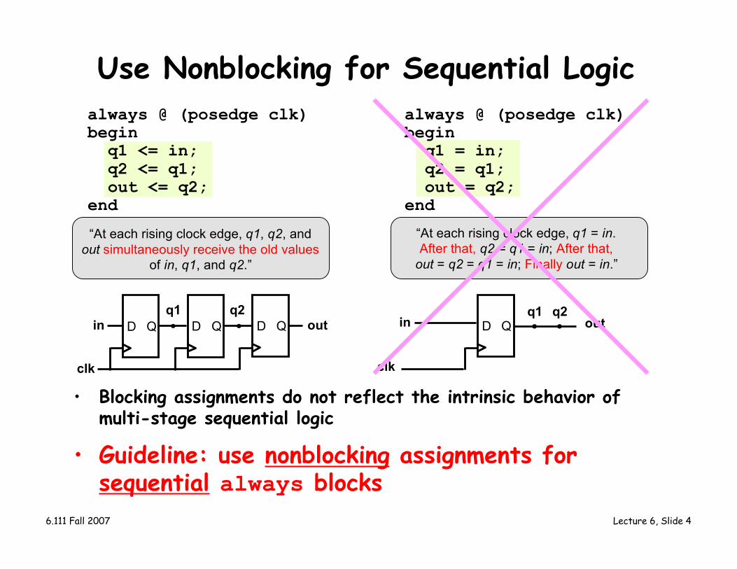
Use Nonblocking for Sequential Logic
D Q D Q D Qin outq1 q2
clk
always @ (posedge clk) begin q1 <= in; q2 <= q1; out <= q2; end
“At each rising clock edge, q1, q2, andout simultaneously receive the old values
of in, q1, and q2.”
always @ (posedge clk) begin q1 = in; q2 = q1; out = q2; end
“At each rising clock edge, q1 = in.After that, q2 = q1 = in; After that,
out = q2 = q1 = in; Finally out = in.”
• Blocking assignments do not reflect the intrinsic behavior ofmulti-stage sequential logic
• Guideline: use nonblocking assignments forsequential always blocks
D Qin out
clk
q1 q2
6.111 Fall 2007 Lecture 6, Slide 5
x <= a & b; 0 1 0 1 1 x<=0
Assignment completion 0 1 0 0 1
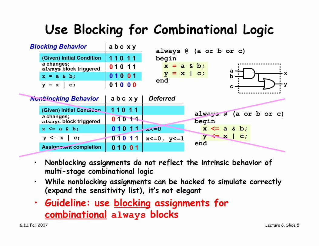
Use Blocking for Combinational Logic
• Nonblocking assignments do not reflect the intrinsic behavior ofmulti-stage combinational logic
• While nonblocking assignments can be hacked to simulate correctly(expand the sensitivity list), it’s not elegant
• Guideline: use blocking assignments forcombinational always blocks
(Given) Initial Condition
Blocking Behavior a b c x y
1 1 0 1 1
(Given) Initial Condition
a b c x y Deferred
1 1 0 1 1
Nonblocking Behavior
always @ (a or b or c) begin x <= a & b; y <= x | c; end
always @ (a or b or c) begin x = a & b; y = x | c; end
ab
c
x
y
a changes;always block triggered 0 1 0 1 1x = a & b; 0 1 0 0 1y = x | c; 0 1 0 0 0
a changes;always block triggered 0 1 0 1 1
y <= x | c; 0 1 0 1 1 x<=0, y<=1
6.111 Fall 2007 Lecture 6, Slide 6
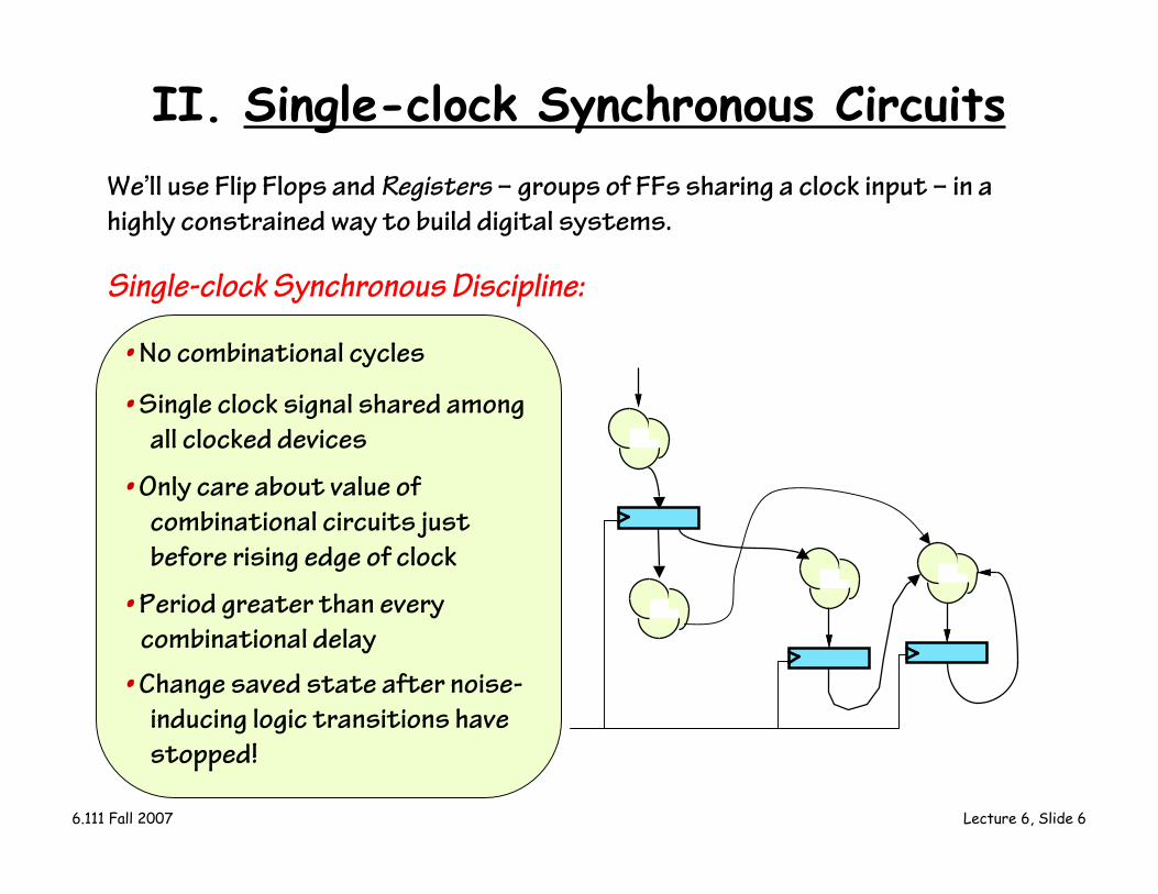
II. Single-clock Synchronous Circuits
Single-clock Synchronous Discipline:
• No combinational cycles
• Only care about value ofcombinational circuits justbefore rising edge of clock
• Period greater than every combinational delay• Change saved state after noise-
inducing logic transitions havestopped!
We’ll use Flip Flops and Registers – groups of FFs sharing a clock input – in ahighly constrained way to build digital systems.
• Single clock signal shared amongall clocked devices
6.111 Fall 2007 Lecture 6, Slide 7
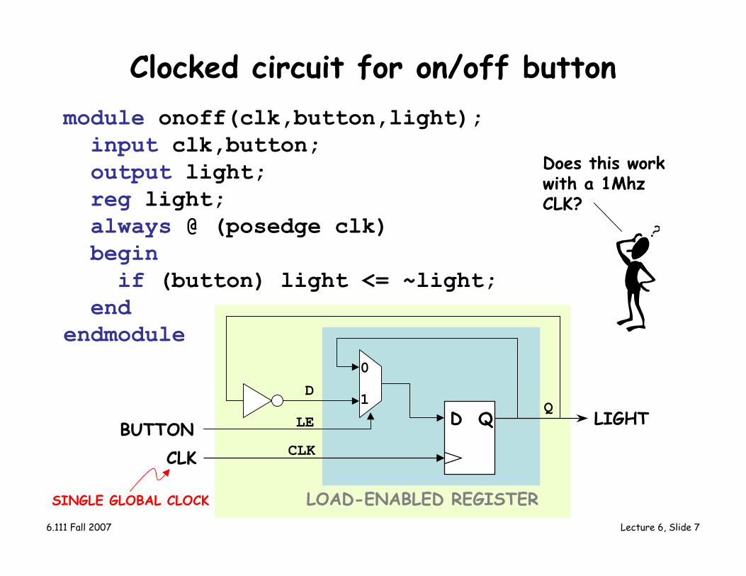
Clocked circuit for on/off buttonmodule onoff(clk,button,light); input clk,button; output light; reg light; always @ (posedge clk) begin if (button) light <= ~light; endendmodule
D QBUTTON LIGHT
CLK
0
1 QD
LE
CLK
LOAD-ENABLED REGISTERSINGLE GLOBAL CLOCK
Does this workwith a 1MhzCLK?
6.111 Fall 2007 Lecture 6, Slide 8
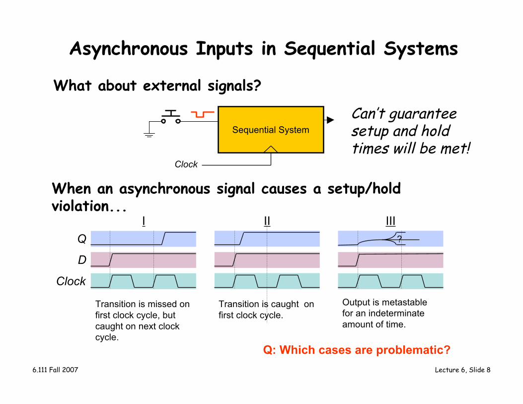
Asynchronous Inputs in Sequential Systems
What about external signals?
Sequential System
Clock
Can’t guaranteesetup and holdtimes will be met!
When an asynchronous signal causes a setup/holdviolation...
Clock
Q
D
I
Transition is missed onfirst clock cycle, butcaught on next clockcycle.
II
Transition is caught onfirst clock cycle.
?
III
Output is metastablefor an indeterminateamount of time.
Q: Which cases are problematic?
6.111 Fall 2007 Lecture 6, Slide 9
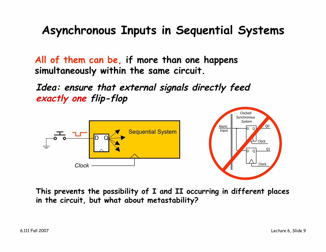
Asynchronous Inputs in Sequential Systems
All of them can be, if more than one happenssimultaneously within the same circuit.
Idea: ensure that external signals directly feedexactly one flip-flop
D QSequential System
Clock
This prevents the possibility of I and II occurring in different placesin the circuit, but what about metastability?
D Q
D Q
Q0
Clock
Clock
Q1
Async Input
Clocked Synchronous
System
6.111 Fall 2007 Lecture 6, Slide 10
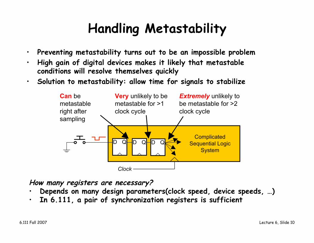
Handling Metastability• Preventing metastability turns out to be an impossible problem• High gain of digital devices makes it likely that metastable
conditions will resolve themselves quickly• Solution to metastability: allow time for signals to stabilize
How many registers are necessary?• Depends on many design parameters(clock speed, device speeds, …)• In 6.111, a pair of synchronization registers is sufficient
D QComplicated
Sequential LogicSystem
Clock
D Q D Q
Can bemetastableright aftersampling
Very unlikely to bemetastable for >1clock cycle
Extremely unlikely tobe metastable for >2clock cycle
6.111 Fall 2007 Lecture 6, Slide 11
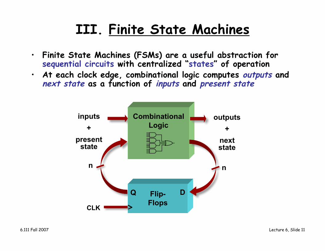
III. Finite State Machines
• Finite State Machines (FSMs) are a useful abstraction forsequential circuits with centralized “states” of operation
• At each clock edge, combinational logic computes outputs andnext state as a function of inputs and present state
CombinationalLogic
Flip-Flops
Q D
CLK
inputs+
presentstate
outputs+
nextstate
n n
6.111 Fall 2007 Lecture 6, Slide 12
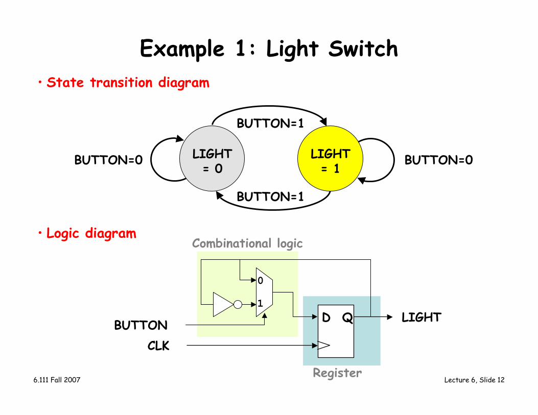
Example 1: Light Switch
LIGHT= 0
LIGHT= 1
BUTTON=1
BUTTON=1
BUTTON=0 BUTTON=0
• State transition diagram
D QBUTTON LIGHT
CLK
0
1
Combinational logic
Register
• Logic diagram
6.111 Fall 2007 Lecture 6, Slide 13
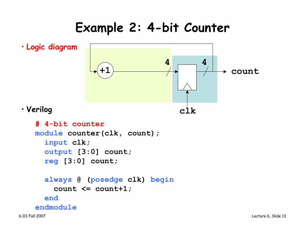
Example 2: 4-bit Counter
+1
clk
count44
• Logic diagram
# 4-bit counter module counter(clk, count); input clk; output [3:0] count; reg [3:0] count;
always @ (posedge clk) begin count <= count+1; endendmodule
• Verilog
6.111 Fall 2007 Lecture 6, Slide 14
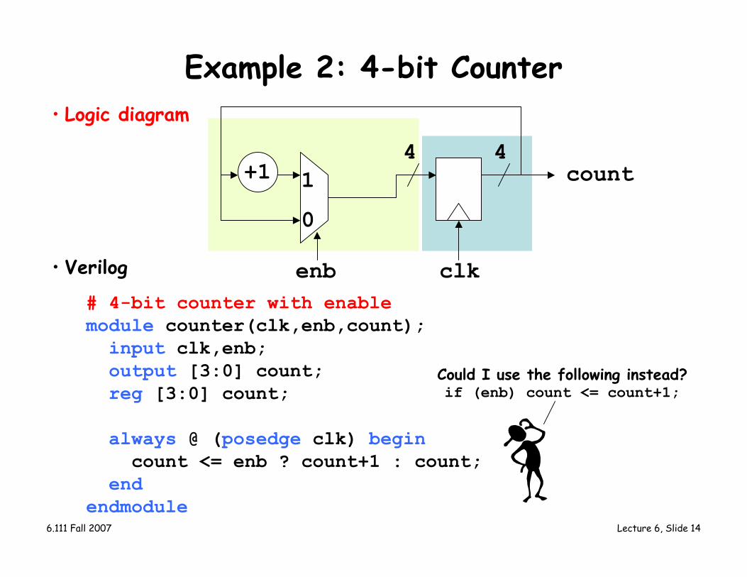
Example 2: 4-bit Counter
1
0
+1
enb clk
count44
• Logic diagram
# 4-bit counter with enablemodule counter(clk,enb,count); input clk,enb; output [3:0] count; reg [3:0] count;
always @ (posedge clk) begin count <= enb ? count+1 : count; endendmodule
• Verilog
Could I use the following instead?if (enb) count <= count+1;
6.111 Fall 2007 Lecture 6, Slide 15
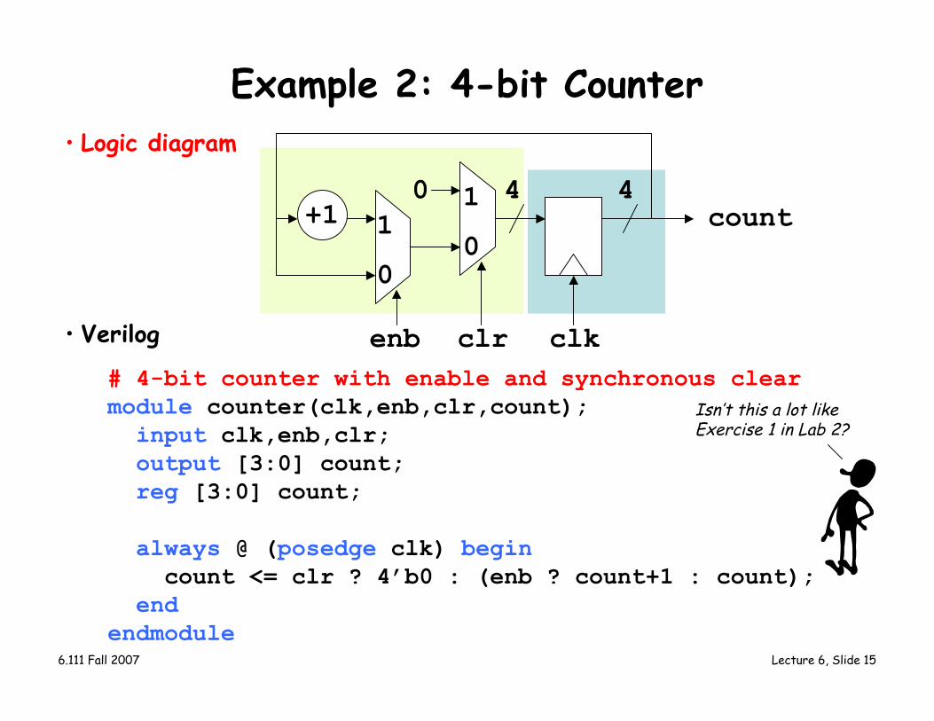
Example 2: 4-bit Counter
0 1
01
0
+1
enb clr clk
count44
Isn’t this a lot likeExercise 1 in Lab 2?
• Logic diagram
# 4-bit counter with enable and synchronous clearmodule counter(clk,enb,clr,count); input clk,enb,clr; output [3:0] count; reg [3:0] count;
always @ (posedge clk) begin count <= clr ? 4’b0 : (enb ? count+1 : count); endendmodule
• Verilog
6.111 Fall 2007 Lecture 6, Slide 16
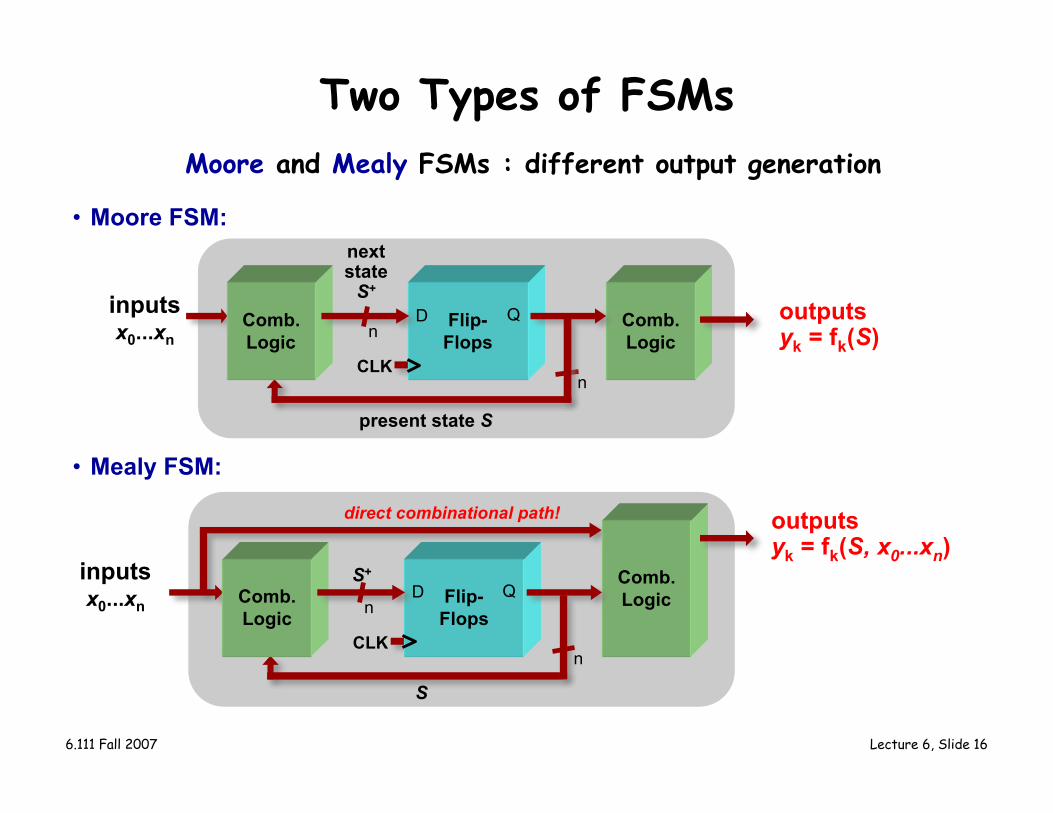
Two Types of FSMsMoore and Mealy FSMs : different output generation
outputsyk = fk(S)
inputsx0...xn
• Moore FSM:
Comb.Logic
CLKn
Flip-Flops
Comb.Logic
D Q
present state S
n
nextstate
S+
inputsx0...xn
• Mealy FSM:
S
Comb.Logic
CLK
Flip-Flops
Comb.LogicD Q
n
S+
n
outputsyk = fk(S, x0...xn)
direct combinational path!
6.111 Fall 2007 Lecture 6, Slide 17
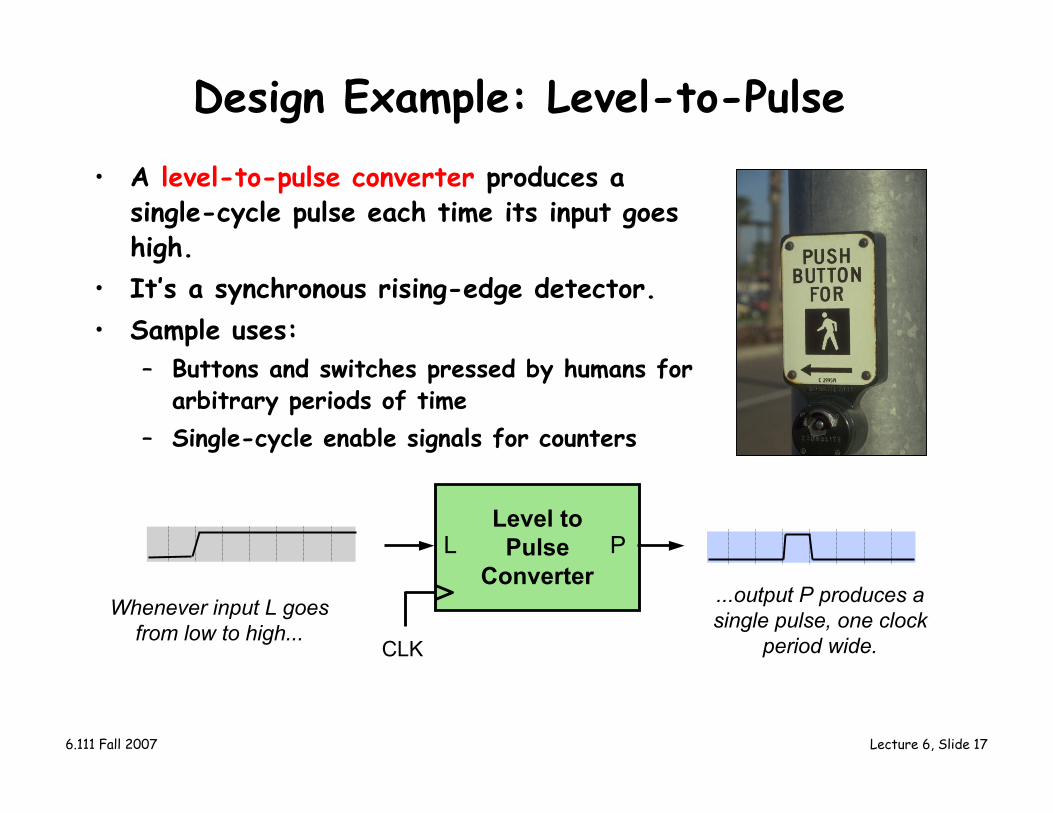
Design Example: Level-to-Pulse
• A level-to-pulse converter produces asingle-cycle pulse each time its input goeshigh.
• It’s a synchronous rising-edge detector.• Sample uses:
– Buttons and switches pressed by humans forarbitrary periods of time
– Single-cycle enable signals for counters
Level toPulse
ConverterL P
CLK
Whenever input L goesfrom low to high...
...output P produces asingle pulse, one clock
period wide.
6.111 Fall 2007 Lecture 6, Slide 18
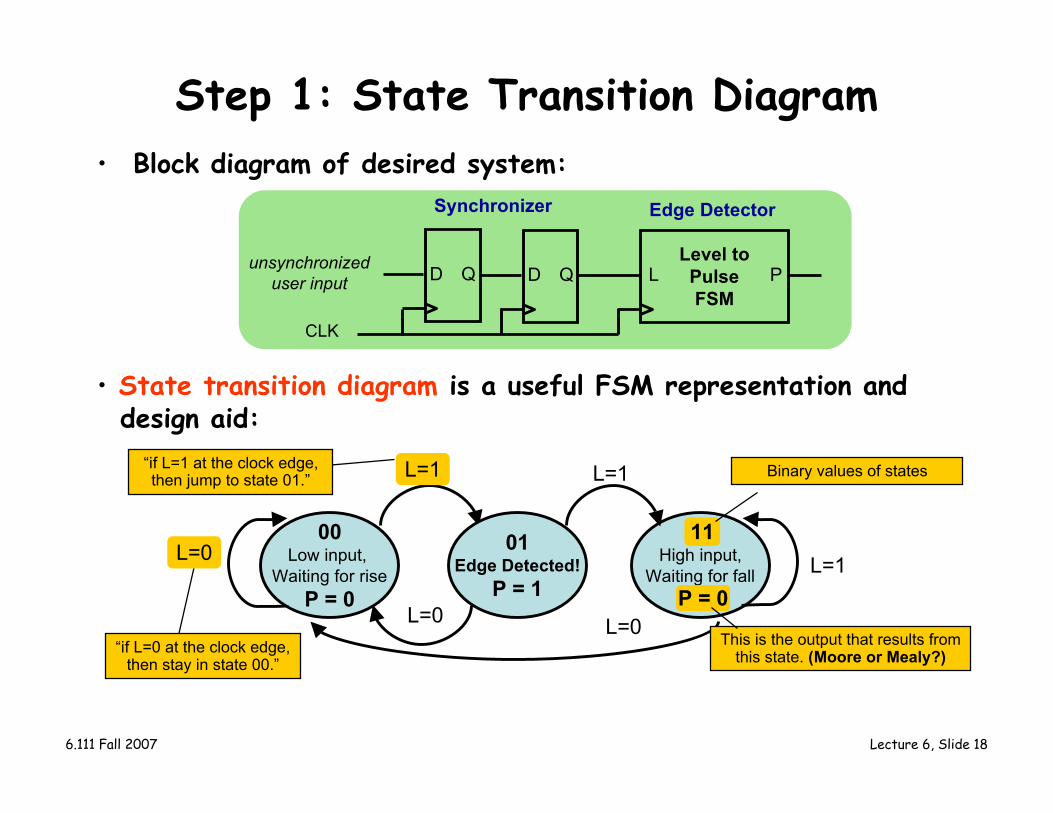
High input,Waiting for fall
11
P = 0
L=1
L=000
Low input, Waiting for rise
P = 0
01Edge Detected!
P = 1
L=1
L=0 L=0
L=1
• State transition diagram is a useful FSM representation and design aid:
Step 1: State Transition Diagram• Block diagram of desired system:
D QLevel toPulseFSM
L Punsynchronized
user input
Synchronizer Edge Detector
This is the output that results fromthis state. (Moore or Mealy?)
P = 0
11
Binary values of states
L=0
“if L=0 at the clock edge,then stay in state 00.”
L=1“if L=1 at the clock edge,then jump to state 01.”
D Q
CLK
6.111 Fall 2007 Lecture 6, Slide 19
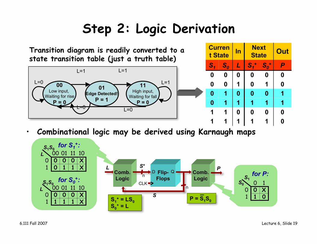
Step 2: Logic Derivation
00Low input,
Waiting for riseP = 0
01Edge Detected!
P = 1
11High input,
Waiting for fallP = 0
L=1 L=1
L=0 L=0
L=1L=0
101010L
In
001100P
Out
101010
S0+
101000
S1+
110000S1
NextState
Current State
1111
00S0
• Combinational logic may be derived using Karnaugh maps
X1101X000010110100
X1111X000010110100
S1S0L
S1S0L
for S1+:
for S0+:
011X0010
S1for P:
S0
Comb.Logic
CLKn
Flip-Flops
Comb.Logic
D Q
S
n
S+L P
S1+ = LS0
S0+ = L
P = S1S0
Transition diagram is readily converted to astate transition table (just a truth table)
6.111 Fall 2007 Lecture 6, Slide 20
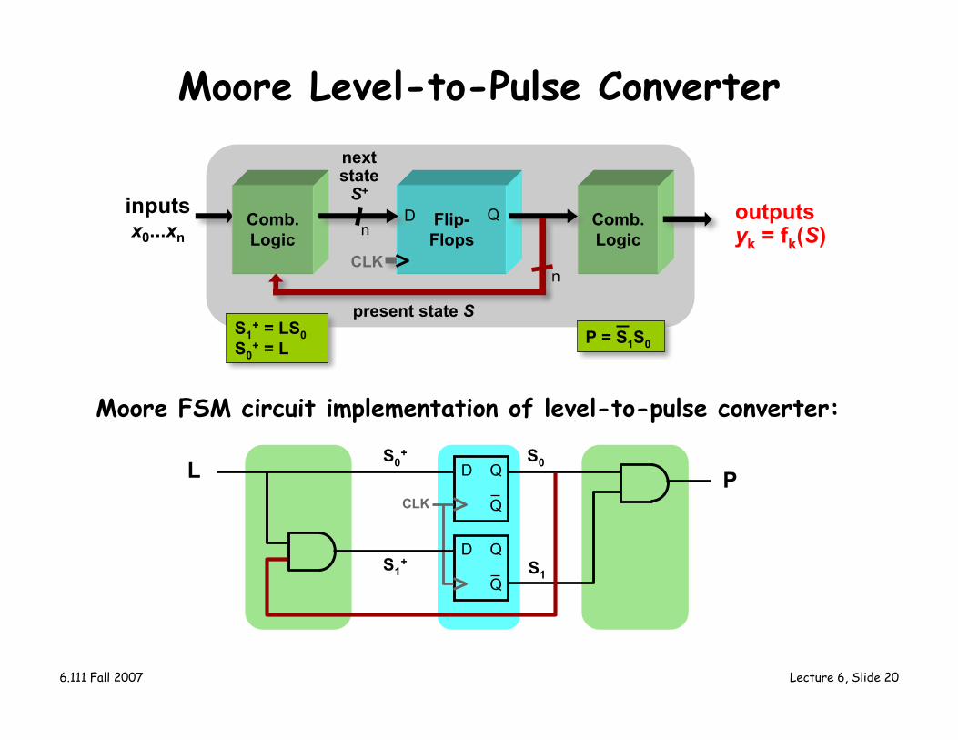
Moore Level-to-Pulse Converter
Moore FSM circuit implementation of level-to-pulse converter:
outputsyk = fk(S)
inputsx0...xn
Comb.Logic
CLKn
Flip-Flops
Comb.Logic
D Q
present state S
n
nextstate
S+
D Q
S1+ = LS0
S0+ = L P = S1S0
D Q
S0
S1
CLK
S0+
S1+
L PQ
Q
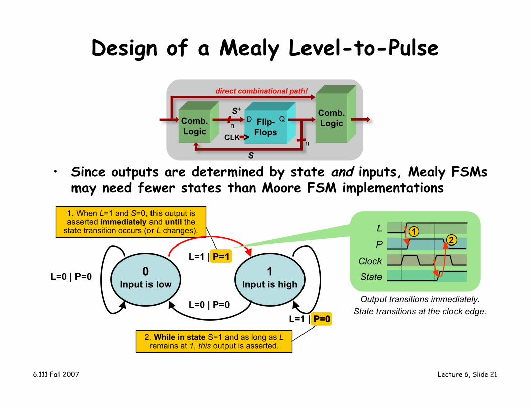
6.111 Fall 2007 Lecture 6, Slide 21
1. When L=1 and S=0, this output isasserted immediately and until the
state transition occurs (or L changes).
2. While in state S=1 and as long as Lremains at 1, this output is asserted.
L=1 | P=0
L=1 | P=1
P=0
0Input is low
1Input is high
L=0 | P=0
L=0 | P=0
Design of a Mealy Level-to-Pulse
• Since outputs are determined by state and inputs, Mealy FSMsmay need fewer states than Moore FSM implementations
S
Comb.Logic
CLK
Flip-Flops
Comb.LogicD Q
n
S+
n
direct combinational path!
P
L
State
Clock
Output transitions immediately.State transitions at the clock edge.
12
6.111 Fall 2007 Lecture 6, Slide 22
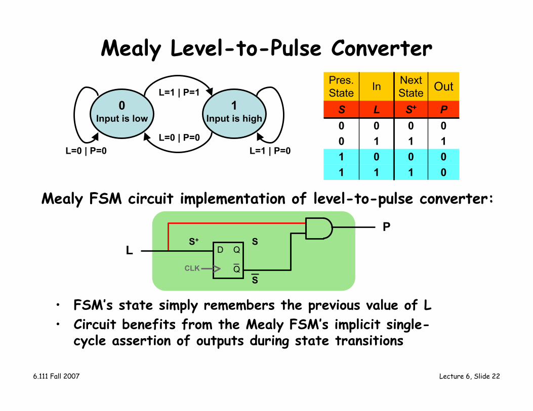
Mealy Level-to-Pulse Converter
Mealy FSM circuit implementation of level-to-pulse converter:
1010L
In
0010P
Out
1010S+
NextState
Pres.State
11
00S
D QS
CLK
S+
L
P
QS
• FSM’s state simply remembers the previous value of L• Circuit benefits from the Mealy FSM’s implicit single-
cycle assertion of outputs during state transitions
0Input is low
1Input is high
L=1 | P=1
L=0 | P=0L=1 | P=0L=0 | P=0

6.111 Fall 2007 Lecture 6, Slide 23
Moore/Mealy Trade-Offs
• How are they different?– Moore: outputs = f( state ) only– Mealy outputs = f( state and input )– Mealy outputs generally occur one cycle earlier than a Moore:
• Compared to a Moore FSM, a Mealy FSM might...– Be more difficult to conceptualize and design– Have fewer states
P
L
State
Clock
Mealy: immediate assertion of P
P
L
State[0]
Clock
Moore: delayed assertion of P
6.111 Fall 2007 Lecture 6, Slide 24
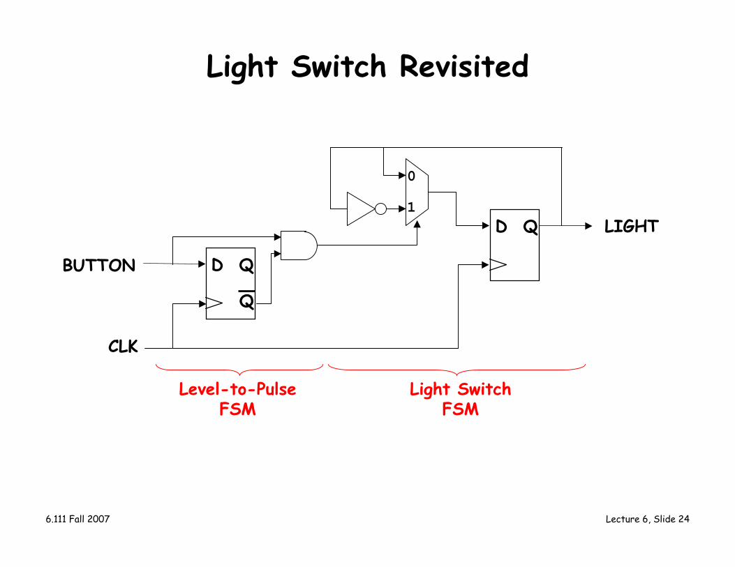
Light Switch Revisited
D Q
BUTTON
LIGHT
CLK
0
1
D Q
Q
Level-to-PulseFSM
Light SwitchFSM