
HYS 72Vxx3xxGR PC133 Registered SDRAM … RDQMB7 DQM CB0-CB7. HYS 72Vxx3xxGR PC133 Registered...
22
INFINEON Technologies 1 6.01 HYS 72Vxx3xxGR PC133 Registered SDRAM-Modules 3.3 V 168-pin Registered SDRAM Modules PC133 128 MByte Module PC133 256 MByte module PC133 512 MByte Module PC133 1 GByte Module PC133 2 GByte Module The HYS 72Vxx3xxGR-7 and -7.5 are industry standard 168-pin 8-byte Dual in-line Memory Modules (DIMMs) organized as 16M × 72, 32M x 72, 64M × 72, 128M × 72 and 256M x 72 high speed memory arrays designed with Synchronous DRAMs (SDRAMs) for ECC applications. The 32M x 72 (256Mbyte) registered DIMM module is available in two versions (12 or 13 row addresses). All control and address signals are registered on-DIMM and the design incorporates a PLL circuit for the Clock inputs. Use of an on-board register reduces capacitive loading on the input signals but are delayed by one cycle in arriving at the SDRAM devices. Decoupling capacitors are mounted on the PC board. The DIMMs use a serial presence detects scheme implemented via a serial E 2 PROM using the 2-pin I 2 C protocol. The first 128 bytes are utilized by the DIMM manufacturer and the second 128 bytes are available to the end user. All Infineon 168-pin DIMMs provide a high performance, flexible 8-byte interface in a 133.35 mm long footprint. • 168-pin Registered 8 Byte Dual-In-Line SDRAM Module for PC and Server main memory applications • One bank 16M × 72, 32M x 72 and 64M × 72 two bank 128M × 72 and 256M x72 organization • Optimized for ECC applications with very low input capacitances • JEDEC standard Synchronous DRAMs (SDRAM) Programmable CAS Latency, Burst Length and Wrap Sequence (Sequential & Interleave) • Single + 3.3 V (± 0.3 V) power supply • Auto Refresh (CBR) and Self Refresh • Programmable CAS Latency, Burst Length, and Wrap Sequence (Sequential & Interleave) • All inputs and outputs are LVTTL compatible • Serial Presence Detect with E 2 PROM • Utilizes SDRAMs in TSOPII-54 packages with registers and PLL. • Card Size: 133.35 mm × 43.18 mm × 4.00/ 6.40 mm with Gold contact pads (JEDEC MO-161) • These modules all fully compatible with the current industry standard PC133 and PC100 specifications • Performance: speed grade -7 -7.5 Unit f CK Clock Frequency (max.) @ CL = 3 133 133 MHz t CK Clock Cycle Time (min.) @ CL = 3 7.5 7.5 ns t AC Clock Access Time (min.) @ CL= 3 5.4 5.4 ns f CK Clock Frequency (max.) @ CL = 2 133 100 MHz t CK Clock Cycle Time (min.) @ CL = 2 7.5 10 ns t AC Clock Access Time (min.) @ CL= 2 5.4 6 ns
Transcript of HYS 72Vxx3xxGR PC133 Registered SDRAM … RDQMB7 DQM CB0-CB7. HYS 72Vxx3xxGR PC133 Registered...
INFINEON Technologies 1 6.01
HYS 72Vxx3xxGRPC133 Registered SDRAM-Modules
3.3 V 168-pin Registered SDRAM Modules
PC133 128 MByte ModulePC133 256 MByte modulePC133 512 MByte ModulePC133 1 GByte ModulePC133 2 GByte Module
The HYS 72Vxx3xxGR-7 and -7.5 are industry standard 168-pin 8-byte Dual in-line Memory Modules (DIMMs)
organized as 16M × 72, 32M x 72, 64M × 72, 128M × 72 and 256M x 72 high speed memory arrays designed with
Synchronous DRAMs (SDRAMs) for ECC applications. The 32M x 72 (256Mbyte) registered DIMM module is
available in two versions (12 or 13 row addresses). All control and address signals are registered on-DIMM and
the design incorporates a PLL circuit for the Clock inputs. Use of an on-board register reduces capacitive loading
on the input signals but are delayed by one cycle in arriving at the SDRAM devices. Decoupling capacitors are
mounted on the PC board. The DIMMs use a serial presence detects scheme implemented via a serial E2PROM
using the 2-pin I2C protocol. The first 128 bytes are utilized by the DIMM manufacturer and the second 128 bytes
are available to the end user. All Infineon 168-pin DIMMs provide a high performance, flexible 8-byte interface in
a 133.35 mm long footprint.
• 168-pin Registered 8 Byte Dual-In-Line SDRAM Module for PC and Server main memory applications
• One bank 16M × 72, 32M x 72 and 64M × 72 two bank 128M × 72 and 256M x72 organization
• Optimized for ECC applications with very low input capacitances
• JEDEC standard Synchronous DRAMs (SDRAM) Programmable CAS Latency, Burst Length and Wrap Sequence (Sequential & Interleave)
• Single + 3.3 V (± 0.3 V) power supply
• Auto Refresh (CBR) and Self Refresh
• Programmable CAS Latency, Burst Length, and Wrap Sequence (Sequential & Interleave)
• All inputs and outputs are LVTTL compatible
• Serial Presence Detect with E2PROM
• Utilizes SDRAMs in TSOPII-54 packages with registers and PLL.
• Card Size: 133.35 mm × 43.18 mm × 4.00/ 6.40 mm with Gold contact pads(JEDEC MO-161)
• These modules all fully compatible with the current industry standard PC133 and PC100 specifications
• Performance:
speed grade -7 -7.5 Unit
fCK Clock Frequency (max.) @ CL = 3 133 133 MHz
tCK Clock Cycle Time (min.) @ CL = 3 7.5 7.5 ns
tAC Clock Access Time (min.) @ CL= 3 5.4 5.4 ns
fCK Clock Frequency (max.) @ CL = 2 133 100 MHz
tCK Clock Cycle Time (min.) @ CL = 2 7.5 10 ns
tAC Clock Access Time (min.) @ CL= 2 5.4 6 ns

HYS 72Vxx3xxGRPC133 Registered SDRAM-Modules
INFINEON Technologies 2 6.01
Ordering Information
Note: All part numbers end with a place code (not shown), designating the die revision. Consult factory for
current revision. Example: HYS 64V16300GR-7.5-C2, indicating Rev.C2 dies are used for SDRAM
components.
Type Compliance Code Description SDRAMTechnology
PC133-333:
HYS 72V16300GR-7.5-CHYS 72V16300GR-7.5-E
PC133R-333-542-B2 one bank 128 MB Reg. DIMM 64 MBit (x4)
HYS 72V16301GR-7.5-C2 PC133R-333-542-B2 one bank 128 MB Reg. DIMM 128 MBit (x8)
HYS 72V32301GR-7.5-C2 PC133R-333-542-B2 one bank 256 MB Reg. DIMM 128 Mbit (x4)
HYS 72V32300GR-7.5-C2HYS 72V32300GR-7.5-D
PC133R-333-542-AA one bank 256 MB Reg. DIMM 256 Mbit (x8)
HYS 72V64300GR-7.5-C2HYS 72V64300GR-7.5-D
PC133R-333-542-B2 one bank 512 MB Reg. DIMM 256 MBit (x4)
HYS 72V128320GR-7.5-C2HYS 72V128320GR-7.5-D
PC133R-333-542-B2 two banks 1 GByte Reg. DIMM 256 MBit(x4, stacked)
HYS 72V256320GR-7.5-A PC133R-333-542-B2 two banks 2 GByte Reg. DIMM 512 MBit(x4, stacked)
PC133-222:
HYS 72V16300GR-7-E PC133R-222-542-B2 one bank 128 MB Reg. DIMM 64 MBit (x4)
HYS 72V16301GR-7-C2 PC133R-222-542-B2 one bank 128 MB Reg. DIMM 128 MBit (x8)
HYS 72V32301GR-7-C2 PC133R-222-542-B2 one bank 256 MB Reg. DIMM 128 Mbit (x4)
HYS 72V32300GR-7-D PC133R-222-542-AA one bank 256 MB Reg. DIMM 256 Mbit (x8)
HYS 72V64300GR-7-D PC133R-222-542-B2 one bank 512 MB Reg. DIMM 256 MBit (x4)
HYS 72V128320GR-7-D PC133R-222-542-B2 two banks 1 GByte Reg. DIMM 256 MBit(x4, stacked)
HYS 72V256320GR-7-A PC133R-222-542-B2 two banks 2 GByte Reg. DIMM 512 MBit(x4, stacked)
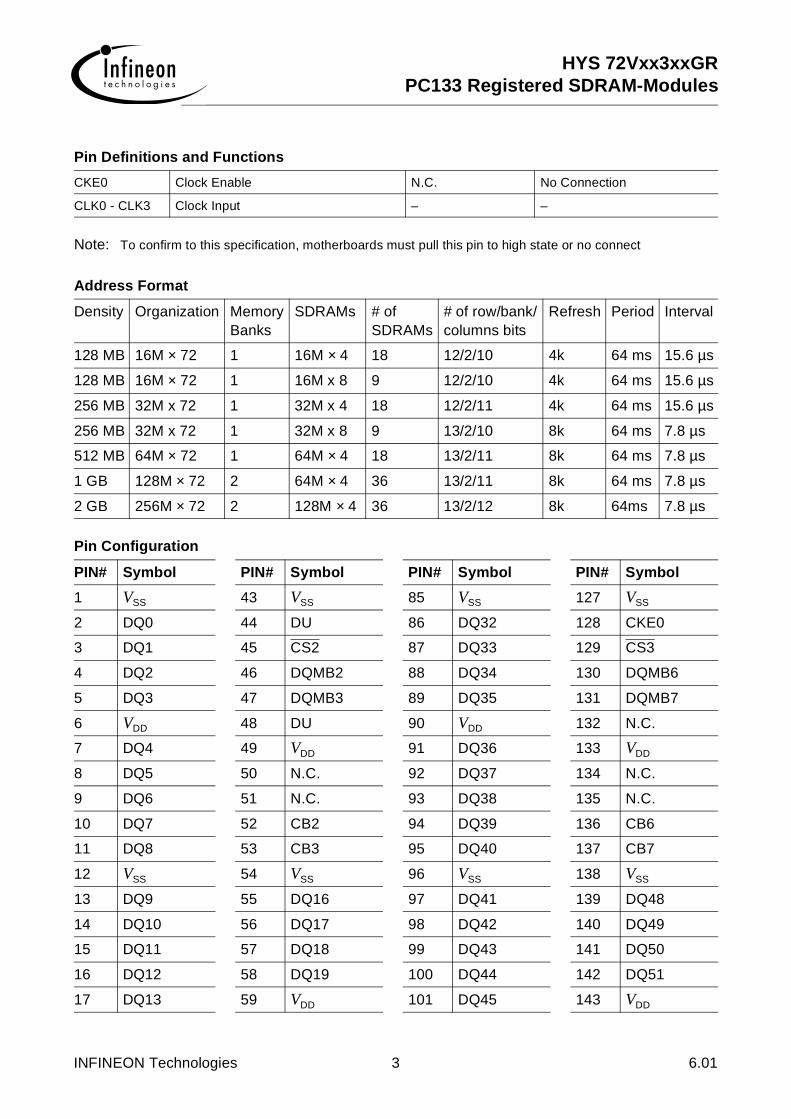
Pin Definitions and Functions
A0 - A11, A12 Address Inputs (A12 is used for 256Mbit based modules only)
DQMB0 - DQMB7 Data Mask
BA0, BA1 Bank Selects CS0 - CS3 Chip Select
DQ0 - DQ63 Data Input/Output REGE*) Register Enable“H” or N.C = registered mode“L” = buffered mode
CB0 - CB7 Check Bits VDD Power (+ 3.3 V)
RAS Row Address Strobe VSS Ground
CAS Column Address Strobe SCL Clock for Presence Detect
WE Read/Write Input SDA Serial Data Out
HYS 72Vxx3xxGRPC133 Registered SDRAM-Modules
INFINEON Technologies 3 6.01
Note: To confirm to this specification, motherboards must pull this pin to high state or no connect
CKE0 Clock Enable N.C. No Connection
CLK0 - CLK3 Clock Input – –
Address Format
Density Organization MemoryBanks
SDRAMs # ofSDRAMs
# of row/bank/columns bits
Refresh Period Interval
128 MB 16M × 72 1 16M × 4 18 12/2/10 4k 64 ms 15.6 µs
128 MB 16M × 72 1 16M x 8 9 12/2/10 4k 64 ms 15.6 µs
256 MB 32M x 72 1 32M x 4 18 12/2/11 4k 64 ms 15.6 µs
256 MB 32M x 72 1 32M x 8 9 13/2/10 8k 64 ms 7.8 µs
512 MB 64M × 72 1 64M × 4 18 13/2/11 8k 64 ms 7.8 µs
1 GB 128M × 72 2 64M × 4 36 13/2/11 8k 64 ms 7.8 µs
2 GB 256M × 72 2 128M × 4 36 13/2/12 8k 64ms 7.8 µs
Pin Configuration
PIN# Symbol PIN# Symbol PIN# Symbol PIN# Symbol
1 VSS 43 VSS 85 VSS 127 VSS
2 DQ0 44 DU 86 DQ32 128 CKE0
3 DQ1 45 CS2 87 DQ33 129 CS3
4 DQ2 46 DQMB2 88 DQ34 130 DQMB6
5 DQ3 47 DQMB3 89 DQ35 131 DQMB7
6 VDD 48 DU 90 VDD 132 N.C.
7 DQ4 49 VDD 91 DQ36 133 VDD
8 DQ5 50 N.C. 92 DQ37 134 N.C.
9 DQ6 51 N.C. 93 DQ38 135 N.C.
10 DQ7 52 CB2 94 DQ39 136 CB6
11 DQ8 53 CB3 95 DQ40 137 CB7
12 VSS 54 VSS 96 VSS 138 VSS
13 DQ9 55 DQ16 97 DQ41 139 DQ48
14 DQ10 56 DQ17 98 DQ42 140 DQ49
15 DQ11 57 DQ18 99 DQ43 141 DQ50
16 DQ12 58 DQ19 100 DQ44 142 DQ51
17 DQ13 59 VDD 101 DQ45 143 VDD
Pin Definitions and Functions
HYS 72Vxx3xxGRPC133 Registered SDRAM-Modules
INFINEON Technologies 4 6.01
18 VDD 60 DQ20 102 VDD 144 DQ52
19 DQ14 61 N.C. 103 DQ46 145 N.C.
20 DQ15 62 DU 104 DQ47 146 DU
21 CB0 63 N.C. 105 CB4 147 REGE
22 CB1 64 VSS 106 CB5 148 VSS
23 VSS 65 DQ21 107 VSS 149 DQ53
24 N.C. 66 DQ22 108 N.C. 150 DQ54
25 N.C. 67 DQ23 109 N.C. 151 DQ55
26 VDD 68 VSS 110 VDD 152 VSS
27 WE 69 DQ24 111 CAS 153 DQ56
28 DQMB0 70 DQ25 112 DQMB4 154 DQ57
29 DQMB1 71 DQ26 113 DQMB5 155 DQ58
30 CS0 72 DQ27 114 CS1 156 DQ59
31 DU 73 VDD 115 RAS 157 VDD
32 VSS 74 DQ28 116 VSS 158 DQ60
33 A0 75 DQ29 117 A1 159 DQ61
34 A2 76 DQ30 118 A3 160 DQ62
35 A4 77 DQ31 119 A5 161 DQ63
36 A6 78 VSS 120 A7 162 VSS
37 A8 79 CLK2 121 A9 163 CLK3
38 A10 (AP) 80 N.C. 122 BA0 164 N.C.
39 BA1 81 WP 123 A11 165 SA0
40 VDD 82 SDA 124 VDD 166 SA1
41 VDD 83 SCL 125 CLK1 167 SA2
42 CLK0 84 VDD 126 A12 168 VDD
Pin Configuration (cont’d)
PIN# Symbol PIN# Symbol PIN# Symbol PIN# Symbol

HYS 72Vxx3xxGRPC133 Registered SDRAM-Modules
INFINEON Technologies 5 6.01
Block Diagram: One Bank 16M × 72, 32M × 72 and 64M × 72 SDRAM DIMM ModulesHYS72V16300GR, HYS72V32301GR and HYS 72V64300GR using x4 organized SDRAMs
SPB04135
DQMDQ0-DQ3
CS
D0
DQMDQ0-DQ3
D1
DQMDQ0-DQ3
D2
DQMDQ0-DQ3
D3
DQMDQ0-DQ3
D16
DQ0-DQ3
DQ4-DQ7
RDQMB1
DQ8-DQ11
DQ12-DQ15
CB0-CB3
RDQMB0RCS0
DQMDQ0-DQ3
D8
DQMDQ0-DQ3
D9
DQMDQ0-DQ3
D10
DQMDQ0-DQ3
D11
DQMDQ0-DQ3
D17
DQ32-DQ35
DQ36-DQ39
RDQMB5
DQ40-DQ43
DQ44-DQ47
CB4-CB7
RDQMB4
DQMDQ0-DQ3
D4
DQMDQ0-DQ3
D5
DQMDQ0-DQ3
D6
DQMDQ0-DQ3
D7
DQ16-DQ19
DQ20-DQ23
RDQMB3
DQ24-DQ27
DQ28-DQ31
RDQMB2RCS2
DQMDQ0-DQ3
D12
DQMDQ0-DQ3
D13
DQMDQ0-DQ3
D14
DQMDQ0-DQ3
D15
DQ48-DQ51
DQ52-DQ55
RDQMB7
DQ56-DQ59
DQ60-DQ63
RDQMB6
CLK012 pF
PLL SDRAMs D0-D17
CLK1, CLK2, CLK312 pF
Reg
iste
r
CS0/CS2DQMB0-7BA0, BA1A0-A11, A12RASCASCKE0WE
RCS0/RCS2RDQMB0-7RBA0, RBA1RA0-RA11, RA12RRASRCASRCKE0RWE
REGE10 kΩ
SDRAMs D0-D17
SDRAMs D0-D17SDRAMs D0-D17SDRAMs D0-D17SDRAMs D0-D17SDRAMs D0-D17
SA0SDA
SA0SA1 SA1
SA2SA2SCLSCL
WP
47 kΩ
E2PROM(256 word x 8 Bit)
VCC
VSS
CD0-D17, Reg., DLL
D0-D17, Reg., DLL
1) DQ wirding may differ from that decribed in this drawing; however DQ/DQB relationship must be maintained as shown2) All resistors are 10 Ω unless otherwise noted
VCC
CS
CS
CS
CS
CS
CS
CS
CS
CS
CS
CS
CS
CS
CS
CS
CS

HYS 72Vxx3xxGRPC133 Registered SDRAM-Modules
INFINEON Technologies 6 6.01
Block Diagram: One Bank 16Mx72 and 32M × 72 ModulesHYS72V16301 & HYS72V32300GR using x8 organized SDRAMs
SPB04130-2
DQ0-DQ7
CS
D0DQ0-DQ7RDQMB0
RCS0
DQ0-DQ7
CS
D4DQ32-DQ39
CLK012 pF
PLL SDRAMs D0-D8
CLK1, CLK2, CLK312 pF
Reg
iste
r
CS0/CS2DQMB0-7BA0, BA1A0-A11,12* )
RASCASCKE0WE
RCS0/RCS2RDQMB0-7RBA0, RBA1RA0-11,12RRASRCASRCKE0RWE
REGE10 kΩ
SDRAMs D0-D8
SDRAMs D0-D8SDRAMs D0-D8SDRAMs D0-D8SDRAMs D0-D8SDRAMs D0-D8
SA0SDA
SA0SA1 SA1
SA2SA2SCLSCL
WP
47 kΩ
E2PROM(256 word x 8 Bit)V
CC
VSS
CD0-D8, Reg., DLL
D0-D8, Reg., DLL
Notes:1 ) DQ wirding may differ from that
decribed in this drawing;however DQ/DQB relationshipmust be maintained as shown
2) All resistors are 10 Ω unlessotherwise noted
*) A12 is only for 32 M x 72organisation
VC C
DQM RDQMB4 DQM
DQ0-DQ7
CS
D1DQ8-DQ15
RDQMB1
DQ0-DQ7
CS
D5DQ40-DQ47
DQM RDQMB5 DQM
DQ0-DQ7
CS
D8
DQMWE
DQ0-DQ7
CS
D2DQ16-DQ23RDQMB2
RCS2
DQ0-DQ7
CS
D6DQ48-DQ55
DQM RDQMB4 DQM
DQ0-DQ7
CS
D3DQ24-DQ31
RDQMB3
DQ0-DQ7
CS
D7DQ56-DQ63
DQM RDQMB7 DQM
CB7CB0-
HYS 72Vxx3xxGRPC133 Registered SDRAM-Modules
INFINEON Technologies 7 6.01
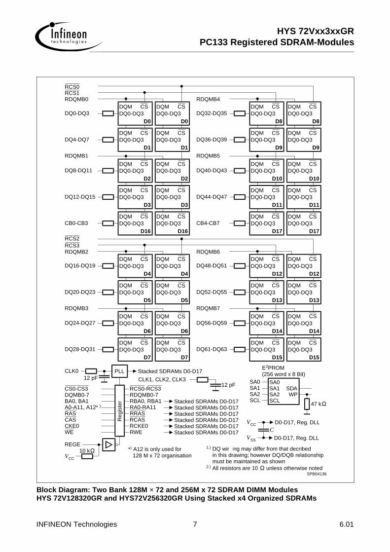
Block Diagram: Two Bank 128M × 72 and 256M x 72 SDRAM DIMM ModulesHYS 72V128320GR and HYS72V256320GR Using Stacked x4 Organized SDRAMs
SPB04136
DQMDQ0-DQ3
D0
DQMDQ0-DQ3
D0
DQMDQ0-DQ3
D1
DQMDQ0-DQ3
D1
DQMDQ0-DQ3
D2
DQMDQ0-DQ3
D2
DQMDQ0-DQ3
D3
DQMDQ0-DQ3
D3
DQMDQ0-DQ3
D16
DQMDQ0-DQ3
D16
DQ0-DQ3
DQ4-DQ7
RDQMB1
DQ8-DQ11
DQ12-DQ15
CB0-CB3
RDQMB0RCS1RCS0
DQMDQ0-DQ3
D8
DQMDQ0-DQ3
D8
DQMDQ0-DQ3
D9
DQMDQ0-DQ3
D9
DQMDQ0-DQ3
D10
DQMDQ0-DQ3
D10
DQMDQ0-DQ3
D11
DQMDQ0-DQ3
D11
DQMDQ0-DQ3
D17
DQMDQ0-DQ3
D17
DQ32-DQ35
DQ36-DQ39
RDQMB5
DQ40-DQ43
DQ44-DQ47
CB4-CB7
RDQMB4
DQMDQ0-DQ3
D4
DQMDQ0-DQ3
D4
DQMDQ0-DQ3
D5
DQMDQ0-DQ3
D5
DQMDQ0-DQ3
D6
DQMDQ0-DQ3
D6
DQMDQ0-DQ3
D7
DQMDQ0-DQ3
D7
DQ16-DQ19
DQ20-DQ23
RDQMB3
DQ24-DQ27
DQ28-DQ31
RDQMB2RCS3RCS2
DQMDQ0-DQ3
D12
DQMDQ0-DQ3
D12
DQMDQ0-DQ3
D13
DQMDQ0-DQ3
D13
DQMDQ0-DQ3
D14
DQMDQ0-DQ3
D14
DQMDQ0-DQ3
D15
DQMDQ0-DQ3
D15
DQ48-DQ51
DQ52-DQ55
RDQMB7
DQ56-DQ59
DQ61-DQ63
RDQMB6
CLK012 pF
PLL Stacked SDRAMs D0-D17
CLK1, CLK2, CLK312 pF
Reg
iste
r
CS0-CS3DQMB0-7BA0, BA1A0-A11, A12* )
RASCASCKE0WE
RCS0-RCS3RDQMB0-7RBA0, RBA1RA0-RA11RRASRCASRCKE0RWE
REGE10 kΩ
Stacked SDRAMs D0-D17
Stacked SDRAMs D0-D17Stacked SDRAMs D0-D17Stacked SDRAMs D0-D17Stacked SDRAMs D0-D17Stacked SDRAMs D0-D17
*) A12 is only used for 128 M x 72 organisation
SA0SDA
SA0SA1 SA1
SA2SA2SCLSCL
WP
E2PROM(256 word x 8 Bit)
VCC
VSS
CD0-D17, Reg. DLL
D0-D17, Reg. DLL
1.) DQ wirding may differ from that decribed in this drawing; however DQ/DQB relationship must be maintained as shown2.) All resistors are 10 Ω unless otherwise noted
VCC
47 kΩ
CSCS
CSCS
CSCS
CSCS
CSCS
CSCS
CSCS
CSCS
CSCS
CSCS
CSCS
CSCS
CSCS
CSCS
CSCS
CSCS
CSCS
CSCS
HYS 72Vxx3xxGRPC133 Registered SDRAM-Modules
INFINEON Technologies 8 6.01
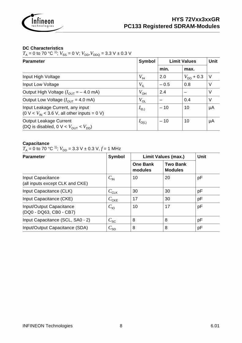
DC CharacteristicsTA = 0 to 70 °C 1); VSS = 0 V; VDD,VDDQ = 3.3 V ± 0.3 V
Parameter Symbol Limit Values Unit
min. max.
Input High Voltage VIH 2.0 VDD + 0.3 V
Input Low Voltage VIL – 0.5 0.8 V
Output High Voltage (IOUT = – 4.0 mA) VOH 2.4 – V
Output Low Voltage (IOUT = 4.0 mA) VOL – 0.4 V
Input Leakage Current, any input(0 V < VIN < 3.6 V, all other inputs = 0 V)
II(L) – 10 10 µA
Output Leakage Current(DQ is disabled, 0 V < VOUT < VDD)
IO(L) – 10 10 µA
CapacitanceTA = 0 to 70 °C 1); VDD = 3.3 V ± 0.3 V, f = 1 MHz
Parameter Symbol Limit Values (max.) Unit
One Bank modules
Two Bank Modules
Input Capacitance(all inputs except CLK and CKE)
CIN 10 20 pF
Input Capacitance (CLK) CCLK 30 30 pF
Input Capacitance (CKE) CCKE 17 30 pF
Input/Output Capacitance(DQ0 - DQ63, CB0 - CB7)
CIO 10 17 pF
Input Capacitance (SCL, SA0 - 2) CSC 8 8 pF
Input/Output Capacitance (SDA) CSD 8 8 pF

HYS 72Vxx3xxGRPC133 Registered SDRAM-Modules
INFINEON Technologies 9 6.01
Operating Currents per SDRAM ComponentTA = 0 to 70 °C 1), VDD = 3.3 V ± 0.3 V(Recommended Operating Conditions unless otherwise noted)
Parameter Test Condition Symbol 64Mb
128Mb
256Mb
512 Mb
Unit Note
max.
Operating current
tRC = tRC(MIN.), tCK = tCK(MIN.)
Outputs open, Burst Length = 4, CL = 3. All banks operated in random access, all banks operated in ping-pong manner to maximize gapless data access
–
ICC1110 160 270 tbd. mA
2)
Precharge stand-by currentin Power Down Mode
CS = VIH(MIN.), CKE ≤ VIL(MAX.)
tCK = min. ICC2P 2 1.5 2 tbd. mA 2)
Precharge Stand-by Currentin Non-Power Down Mode
CS = VIH (MIN.), CKE ≥ VIH(MIN.)
tCK = min. ICC2N 40 40 25 tbd. mA 2)
No operating current
tCK = min., CS = VIH(MIN.),active state (max. 4 banks)
CKE ≥ VIH(MIN.) ICC3N 50 50 50 tbd. mA 2)
CKE ≤ VIL(MAX.) ICC3P 8 10 10 tbd. mA 2)
Burst operating currenttCK = min.,Read command cycling
– ICC4
70 100 170 tbd. mA
2), 3)
Auto refresh currenttCK = min.,Auto Refresh command cycling
– ICC5 140 230 240 tbd. mA 2)
Self refresh currentSelf Refresh Mode,CKE = 0.2 V
– ICC6 1 1.5 2.5 tbd. mA 2)
HYS 72Vxx3xxGRPC133 Registered SDRAM-Modules
INFINEON Technologies 10 6.01
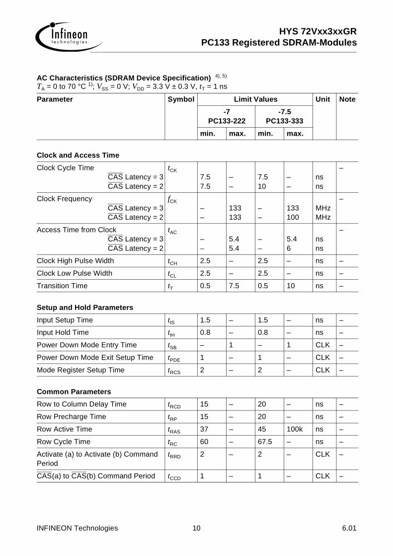
AC Characteristics (SDRAM Device Specification) 4), 5)
TA = 0 to 70 °C 1); VSS = 0 V; VDD = 3.3 V ± 0.3 V, tT = 1 ns
Parameter Symbol Limit Values Unit Note
-7PC133-222
-7.5PC133-333
min. max. min. max.
Clock and Access Time
Clock Cycle TimeCAS Latency = 3CAS Latency = 2
tCK
7.57.5
––
7.510
––
nsns
–
Clock Frequency CAS Latency = 3CAS Latency = 2
fCK
––
133133
––
133100
MHzMHz
–
Access Time from ClockCAS Latency = 3CAS Latency = 2
tAC
––
5.45.4
––
5.46
nsns
–
Clock High Pulse Width tCH 2.5 – 2.5 – ns –
Clock Low Pulse Width tCL 2.5 – 2.5 – ns –
Transition Time tT 0.5 7.5 0.5 10 ns –
Setup and Hold Parameters
Input Setup Time tIS 1.5 – 1.5 – ns –
Input Hold Time tIH 0.8 – 0.8 – ns –
Power Down Mode Entry Time tSB – 1 – 1 CLK –
Power Down Mode Exit Setup Time tPDE 1 – 1 – CLK –
Mode Register Setup Time tRCS 2 – 2 – CLK –
Common Parameters
Row to Column Delay Time tRCD 15 – 20 – ns –
Row Precharge Time tRP 15 – 20 – ns –
Row Active Time tRAS 37 – 45 100k ns –
Row Cycle Time tRC 60 – 67.5 – ns –
Activate (a) to Activate (b) Command Period
tRRD 2 – 2 – CLK –
CAS(a) to CAS(b) Command Period tCCD 1 – 1 – CLK –

HYS 72Vxx3xxGRPC133 Registered SDRAM-Modules
INFINEON Technologies 11 6.01
Refresh Cycle
Refresh Period64&128MBit SDRAM Based Modules
256 MBit SDRAM Based Modules
tREF
––
15.67.8
––
15.67.8
µsµs
–
Self Refresh Exit Time tSREX 1 – 1 – CLK 6)
Read Cycle
Data Out Hold Time tOH 3 – 3 – ns –
Data Out to Low Impedance Time tLZ 0 – 0 – ns 7)
Data Out to High Impedance Time tHZ 3 7 3 7 ns 7)
DQM Data Out Disable Latency tDQZ – 2 – 2 CLK –
Write Cycle
Data Input to Precharge(write recovery)
tWR 2 – 2 – CLK –
DQM Write Mask Latency tDQW 0 – 0 – CLK –
AC Characteristics (SDRAM Device Specification) (cont’d) 4), 5)
TA = 0 to 70 °C 1); VSS = 0 V; VDD = 3.3 V ± 0.3 V, tT = 1 ns
Parameter Symbol Limit Values Unit Note
-7PC133-222
-7.5PC133-333
min. max. min. max.

HYS 72Vxx3xxGRPC133 Registered SDRAM-Modules
INFINEON Technologies 12 6.01
Notes
1. The registered DIMM modules are designed to operate under system operating conditionsbetween 0-55 deg C ambient, maximum sustained bandwidth and 0 LFM airflow.
2. These parameters depend on the cycle rate. All values are measured at 133 MHz operationfrequency. Input signals are changed once during tck excepts for Icc6 and for standby currentswhen tck = infinity.
3. These parameters are measured with continous data stream during read access and all DQtoggling. CL=3 and BL=4 is assumed and the Vcc current is excluded.
4. An initial pause of 100 µs is required after power-up. Then a Precharge All Banks command mustbe given followed by eight Auto Refresh (CBR) cycles before the Mode Register Set Operationcan begin. Also the on-DIMM PLL must be given enough clock cycles to stabilize (tSTAB) beforeany operation can be guaranteed.
5. AC timing tests have VIL = 0.8 V and VIH = 2.0 V with the timing referenced to the 1.4 V crossoverpoint. The transition time is measured between VIH and VIL. All AC measurements assumetT = 1 ns with the AC output load circuit shown. Specified tAC and tOH parameters are measuredwith a 50 pF only, without any resistive termination and with a input signal of 1 V/ns edge ratebetween 0.8 V and 2.0 V.
6. Self Refresh Exit is a synchronous operation and begins on the second positive clock edge afterCKE returns high. Self Refresh Exit is not complete until a time period equal to tRC is satisfiedafter the Self Refresh Exit command is registered.
7. Referenced to the time at which the output achieves the open circuit condition, not to outputvoltage levels.
A serial presence detect storage device - E2PROM 34C02 - is assembled onto the module. Information about the module configuration, speed, etc. is written into the E2PROM device during module production using a serial presence detect protocol (I2C synchronous 2-wire bus).
50 pF
I/O
Measurement conditions fortAC and tOH
SPT03404
CLOCK2.4 V0.4 V
INPUT
HOLDtSETUPt
t T
OUTPUT 1.4 V
t LZ
ACt tAC
OHt
HZt
1.4 V
CLt
CHt
HYS 72Vxx3xxGRPC133 Registered SDRAM-Modules
INFINEON Technologies 13 6.01
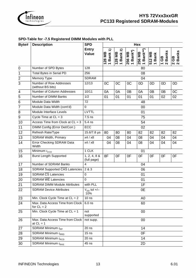
SPD-Table for -7.5 Registered DIMM Modules with PLL
Byte# Description SPD Entry Value
Hex
128
MB
1B
ank
1)
128
MB
1B
ank
2)
256
MB
1B
ank*
)
256
MB
1B
ank*
*)
512
MB
1
Ban
k
1G
B2
Ban
ks
2G
B2
Ban
ks
0 Number of SPD Bytes 128 801 Total Bytes in Serial PD 256 082 Memory Type SDRAM 043 Number of Row Addresses
(without BS bits)12/13 0C 0C 0C 0D 0D 0D 0D
4 Number of Column Addresses 10/11 0A 0A 0B 0A 0B 0B 0C5 Number of DIMM Banks 1/2 01 01 01 01 01 02 026 Module Data Width 72 487 Module Data Width (cont’d) 0 008 Module Interface Levels LVTTL 019 Cycle Time at CL = 3 7.5 ns 7510 Access Time from Clock at CL = 3 5.4 ns 5411 DIMM Config (Error Det/Corr.) ECC 0212 Refresh Rate/Type 15.6/7.8 µs 80 80 80 82 82 82 8213 SDRAM Width, Primary x4 / x8 04 08 04 08 04 04 0414 Error Checking SDRAM Data
Widthx4 / x8 04 08 04 08 04 04 04
15 Minimum tCCD 1 CLK 0116 Burst Length Supported 1, 2, 4, 8 &
(full page)8F 0F 0F 0F 0F 0F 0F
17 Number of SDRAM Banks 4 0418 SDRAM Supported CAS Latencies 2 & 3 0619 SDRAM CS Latencies 0 0120 SDRAM WE Latencies 0 0121 SDRAM DIMM Module Attributes with PLL 1F22 SDRAM Device Attributes VDD tol +/–
10%0E
23 Min. Clock Cycle Time at CL = 2 10 ns A024 Max. Data Access Time from Clock
for CL = 26.0 ns 60
25 Min. Clock Cycle Time at CL = 1 not supported
00
26 Max. Data Access Time from Clock at CL = 1
not supp. 00
27 SDRAM Minimum tRP 20 ns 1428 SDRAM Minimum tRRD 15 ns 0F29 SDRAM Minimum tRCD 20 ns 1430 SDRAM Minimum tRAS 45 ns 2D
HYS 72Vxx3xxGRPC133 Registered SDRAM-Modules
INFINEON Technologies 14 6.01
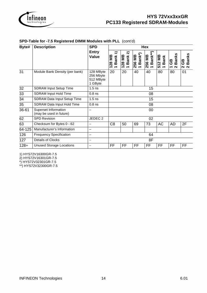
1) HYS72V16300GR-7.52) HYS72V16301GR-7.5*) HYS72V32301GR-7.5**) HYS72V32300GR-7.5
31 Module Bank Density (per bank) 128 MByte256 Mbyte 512 MByte1 GByte
20 20 40 40 80 80 01
32 SDRAM Input Setup Time 1.5 ns 1533 SDRAM Input Hold Time 0.8 ns 0834 SDRAM Data Input Setup Time 1.5 ns 1535 SDRAM Data Input Hold Time 0.8 ns 0836-61 Superset Information
(may be used in future)– 00
62 SPD Revision JEDEC 2 0263 Checksum for Bytes 0 - 62 – C8 50 69 73 AC AD 2F64-125 Manufacturer’s Information –
126 Frequency Specification – 64127 Details of Clocks – 8F128+ Unused Storage Locations – FF FF FF FF FF FF FF
SPD-Table for -7.5 Registered DIMM Modules with PLL (cont’d)
Byte# Description SPD Entry Value
Hex
128
MB
1B
ank
1)
128
MB
1B
ank
2)
256
MB
1B
ank*
)
256
MB
1B
ank*
*)
512
MB
1
Ban
k
1G
B2
Ban
ks
2G
B2
Ban
ks

HYS 72Vxx3xxGRPC133 Registered SDRAM-Modules
INFINEON Technologies 15 6.01
SPD-Table for -7 Registered DIMM Modules with PLL
Byte# Description SPD Entry Value
Hex
128
MB
1B
ank
1)
128
MB
1B
ank
2)
256
MB
1B
ank*
)
256
MB
1B
ank*
*)
512
MB
1
Ban
k
1G
B2
Ban
ks
2G
B2
Ban
ks
0 Number of SPD Bytes 128 801 Total Bytes in Serial PD 256 082 Memory Type SDRAM 043 Number of Row Addresses
(without BS bits)12/13 0C 0C 0C 0D 0D 0D 0D
4 Number of Column Addresses 10/11 0A 0A 0B 0A 0B 0B 0C5 Number of DIMM Banks 1/2 01 01 01 01 01 02 026 Module Data Width 72 487 Module Data Width (cont’d) 0 008 Module Interface Levels LVTTL 019 Cycle Time at CL = 3 7.5 ns 7510 Access Time from Clock at CL = 3 5.4 ns 5411 DIMM Config (Error Det/Corr.) ECC 0212 Refresh Rate/Type 15.6/7.8 µs 80 80 80 82 82 82 8213 SDRAM Width, Primary x4 / x8 04 08 04 08 04 04 0414 Error Checking SDRAM Data
Widthx4 / x8 04 08 04 08 04 04 04
15 Minimum tCCD 1 CLK 0116 Burst Length Supported 1, 2, 4, 8 &
(full page)8F 0F 0F 0F 0F 0F 0F
17 Number of SDRAM Banks 4 0418 SDRAM Supported CAS Latencies 2 & 3 0619 SDRAM CS Latencies 0 0120 SDRAM WE Latencies 0 0121 SDRAM DIMM Module Attributes with PLL 1F22 SDRAM Device Attributes VDD tol +/–
10%0E
23 Min. Clock Cycle Time at CL = 2 7.5 ns 7524 Max. Data Access Time from Clock
for CL = 25.6 ns 54
25 Min. Clock Cycle Time at CL = 1 not supported
00
26 Max. Data Access Time from Clock at CL = 1
not supp. 00
27 SDRAM Minimum tRP 15 ns 0F28 SDRAM Minimum tRRD 14 ns 0E29 SDRAM Minimum tRCD 15 ns 0F30 SDRAM Minimum tRAS 37 ns 25
HYS 72Vxx3xxGRPC133 Registered SDRAM-Modules
INFINEON Technologies 16 6.01
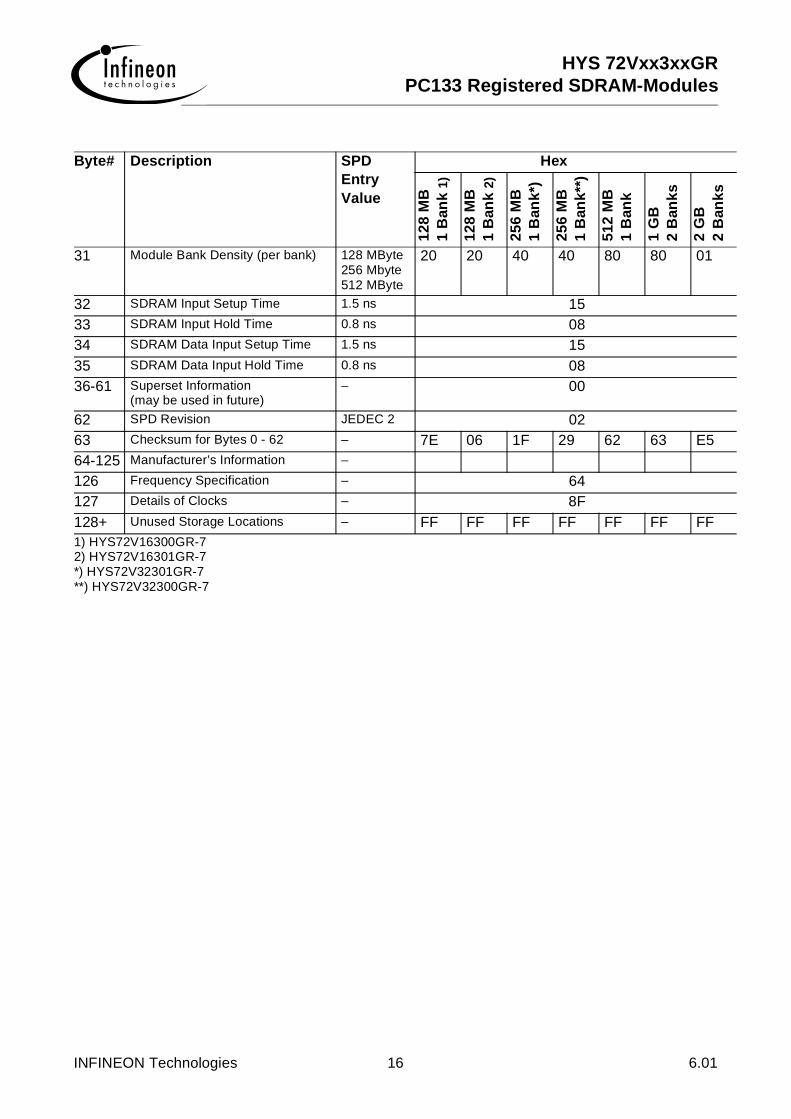
1) HYS72V16300GR-72) HYS72V16301GR-7*) HYS72V32301GR-7**) HYS72V32300GR-7
31 Module Bank Density (per bank) 128 MByte256 Mbyte512 MByte
20 20 40 40 80 80 01
32 SDRAM Input Setup Time 1.5 ns 1533 SDRAM Input Hold Time 0.8 ns 0834 SDRAM Data Input Setup Time 1.5 ns 1535 SDRAM Data Input Hold Time 0.8 ns 0836-61 Superset Information
(may be used in future)– 00
62 SPD Revision JEDEC 2 0263 Checksum for Bytes 0 - 62 – 7E 06 1F 29 62 63 E564-125 Manufacturer’s Information –
126 Frequency Specification – 64127 Details of Clocks – 8F128+ Unused Storage Locations – FF FF FF FF FF FF FF
Byte# Description SPD Entry Value
Hex
128
MB
1B
ank
1)
128
MB
1B
ank
2)
256
MB
1B
ank*
)
256
MB
1B
ank*
*)
512
MB
1
Ban
k
1G
B2
Ban
ks
2G
B2
Ban
ks

HYS 72Vxx3xxGRPC133 Registered SDRAM-Modules
INFINEON Technologies 17 6.01
Package Outlines
Module PackageJEDEC MO-161Registered DIMM Modules Raw Card AA L-DIM168-44
128MB & 256MB modules based on x8 SDRAM components
note: all outline dimensions and tolerances are in accordance with the JEDEC standard
133.35
10 113 6.35 6.35
4140
42.18
84
127.35
3
1.27 0.1±
85 94 95 124 125 168
2
17.7
83.
125
±0.
14
4
38.1
0
Detail of Contacts
min
.2.
54
1+0.5
1.27
1
1.27
66.68
0.25
max
.
PLL RegisterRegister
L-DIM-168-44

HYS 72Vxx3xxGRPC133 Registered SDRAM-Modules
INFINEON Technologies 18 6.01
Package Outlines
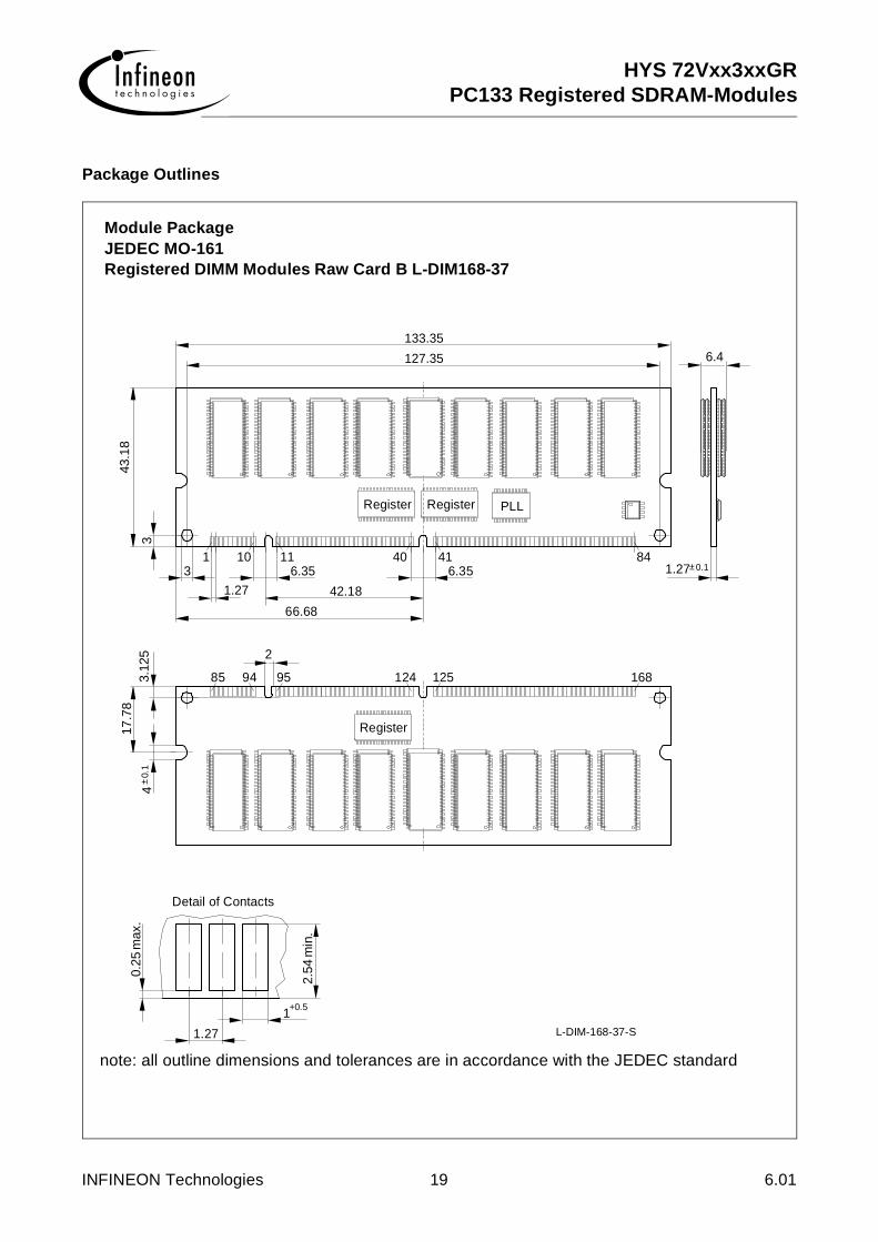
Module PackageJEDEC MO-161Registered DIMM Modules Raw Card B L-DIM168-37
128MB, 256MB & 512MB modules based on x4 SDRAM components
note: all outline dimensions and tolerances are in accordance with the JEDEC standard
133.35
10 113 6.35 6.35
4140
42.18
84
127.35
3
1.27 0.1±
85 94 95 124 125 168
2
17.7
83.
125
±0.
14
4
43.1
8
Detail of Contacts
min
.2.
54
1+0.5
1.27
1
1.27
66.68
0.25
max
.
PLLRegisterRegister
L-DIM-168-37
Register
HYS 72Vxx3xxGRPC133 Registered SDRAM-Modules
INFINEON Technologies 19 6.01
Package Outlines
Module PackageJEDEC MO-161Registered DIMM Modules Raw Card B L-DIM168-37
note: all outline dimensions and tolerances are in accordance with the JEDEC standard
133.35
10 113 6.35 6.35
4140
42.18
84
127.35
3
1.27 0.1±
85 94 95 124 125 168
2
17.7
83.
125
±0.
14
6.4
43.1
8
Detail of Contacts
min
.2.
54
1+0.5
1.27
1
1.27
66.68
0.25
max
.
PLLRegister
L-DIM-168-37-S
Register
Register
HYS 72Vxx3xxGRPC133 Registered SDRAM-Modules
INFINEON Technologies 20 6.01
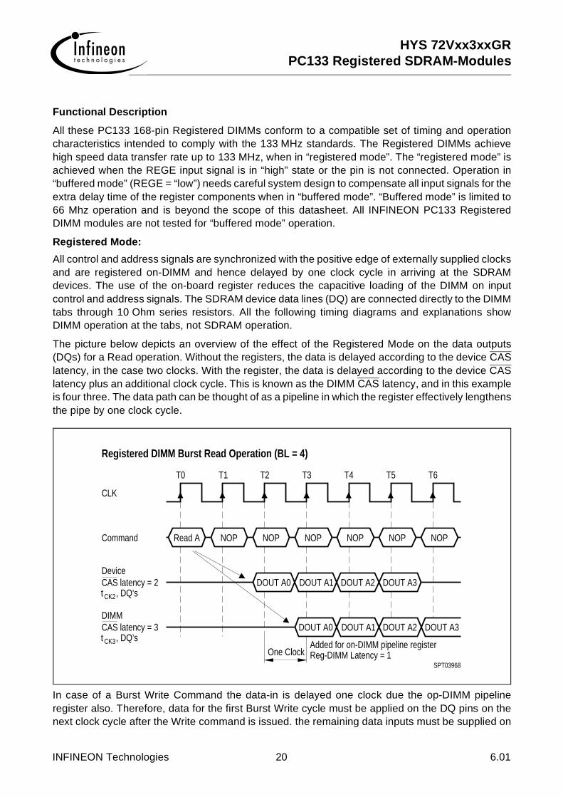
Functional Description
All these PC133 168-pin Registered DIMMs conform to a compatible set of timing and operationcharacteristics intended to comply with the 133 MHz standards. The Registered DIMMs achievehigh speed data transfer rate up to 133 MHz, when in “registered mode”. The “registered mode” isachieved when the REGE input signal is in “high” state or the pin is not connected. Operation in“buffered mode” (REGE = “low”) needs careful system design to compensate all input signals for theextra delay time of the register components when in “buffered mode”. “Buffered mode” is limited to66 Mhz operation and is beyond the scope of this datasheet. All INFINEON PC133 RegisteredDIMM modules are not tested for “buffered mode” operation.
Registered Mode:
All control and address signals are synchronized with the positive edge of externally supplied clocksand are registered on-DIMM and hence delayed by one clock cycle in arriving at the SDRAMdevices. The use of the on-board register reduces the capacitive loading of the DIMM on inputcontrol and address signals. The SDRAM device data lines (DQ) are connected directly to the DIMMtabs through 10 Ohm series resistors. All the following timing diagrams and explanations showDIMM operation at the tabs, not SDRAM operation.
The picture below depicts an overview of the effect of the Registered Mode on the data outputs(DQs) for a Read operation. Without the registers, the data is delayed according to the device CASlatency, in the case two clocks. With the register, the data is delayed according to the device CASlatency plus an additional clock cycle. This is known as the DIMM CAS latency, and in this exampleis four three. The data path can be thought of as a pipeline in which the register effectively lengthensthe pipe by one clock cycle.
In case of a Burst Write Command the data-in is delayed one clock due the op-DIMM pipelineregister also. Therefore, data for the first Burst Write cycle must be applied on the DQ pins on thenext clock cycle after the Write command is issued. the remaining data inputs must be supplied on
SPT03968
CLK
Read A
T0 T1 T2 T3 T4 T5 T6
Command
DOUT A0 DOUT A1 DOUT A2 DOUT A3
NOP NOP NOP NOP NOP
CAS latency = 2, DQ’sCK2t
Registered DIMM Burst Read Operation (BL = 4)
Device
NOP
DOUT A1DOUT A0 DOUT A2 DOUT A3CAS latency = 3DIMM
, DQ’sCK3tOne Clock
Added for on-DIMM pipeline registerReg-DIMM Latency = 1
HYS 72Vxx3xxGRPC133 Registered SDRAM-Modules
INFINEON Technologies 21 6.01
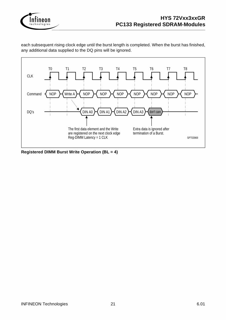
each subsequent rising clock edge until the burst length is completed. When the burst has finished,any additional data supplied to the DQ pins will be ignored.
Registered DIMM Burst Write Operation (BL = 4)
DQ’s
The first data element and the Writeare registered on the next clock edgeReg-DIMM Latency = 1 CLK
DIN A0 DIN A1
Extra data is ignored aftertermination of a Burst.
don’t careDIN A2 DIN A3
SPT03969
T8
NOP
CLK
Command NOP
T0
Write A
T1
NOP
T2
NOP
T3 T6
NOP
T4
NOP
T5 T7
NOP NOP

INFINEON Technologies
Attention please !
As far as patents or other rights of third parties are concerned, liability is onlyassumed for components, not for applications, processes and circuits implementedwithin components or assemblies. This infomation describes the type ofcomponents and shall not be considered as assured characteristics. Terms ofdelivery and rights to change design reserved.
For questions on technology, delivery and prices please contact INFINEONTechnologies Offices in Munich or the INFINEON Technologies Sales Offices andRepresentatives worldwide.
Due to technical requirements components may contain dangerous substances.For information on the types in question please contact your nearest INFINEONTechnologies office or representative.
Packing
Please use the recycling operators known to you. We can help you - get in touchwith your nearest sales office. By agreement we will take packing material back, ifit is sorted. You must bear the costs of transport. For packing material that isreturned to us unsorted or which we are not obliged to accept, we shall have toinvoice you for any costs incurred.
Components used in life-support devices or systems must beexpressly authorized for such purpose!
Ciritcal components1 of INFINEON Technologies, may only be used in life-supportdevices or systems2 with the express written approval of INFINEON Technologies.
1. A critical component is a component used in a life-support device or systemwhose failure can reasonably be expected to cause the failure of that life-supportdevice or system, or to affect its safety or effectiveness of that device or system.
2. Life support devices or systems are intended (a) to be implanted in the humanbody, or (b) to support and/or maintain and sustain human life. If they fail, it isreasonable to assume that the health of the user may be endangered.