Hydrogen Gas Sensing with Networks of Ultrasmall Palladium
7
Hydrogen Gas Sensing with Networks of Ultrasmall Palladium Nanowires Formed on Filtration Membranes X. Q. Zeng, †,‡ M. L. Latimer, †,§ Z. L. Xiao,* ,†,§ S. Panuganti, § U. Welp, † W. K. Kwok, † and T. Xu ‡ † Materials Science Division, Argonne National Laboratory, Argonne, Illinois 60439, United States and ‡ Department of Chemistry and Biochemistry and § Department of Physics, Northern Illinois University, DeKalb, Illinois 60115, United States ABSTRACT Hydrogen sensors based on single Pd nanowires show promising results in speed, sensitivity, and ultralow power consumption. The utilization of single Pd nanowires, however, face challenges in nanofabrication, manipulation, and achieving ultrasmall transverse dimensions. We report on hydrogen sensors that take advantage of single palladium nanowires in high speed and sensitivity and that can be fabricated conveniently. The sensors are based on networks of ultrasmall (<10 nm) palladium nanowires deposited onto commercially available filtration membranes. We investigated the sensitivities and response times of these sensors as a function of the thickness of the nanowires and also compared them with a continuous reference film. The superior performance of the ultrasmall Pd nanowire network based sensors demonstrates the novelty of our fabrication approach, which can be directly applied to palladium alloy and other hydrogen sensing materials. KEYWORDS Hydrogen sensor, palladium, nanowires, networks H ydrogen (H 2 ) gas is considered to be one of the most promising clean energy carriers for use in fuel cells and combustion engines. 1 It is also used extensively in scientific research and industry, notably in glass and steel manufacturing as well as in the refining of petroleum prod- ucts. 2 Effective H 2 sensors that can quickly and sensitively respond to H 2 gas are crucial for the safe deployment of all hydrogen-based applications. Large scale industrial sensing has been achieved using gas chromatography or mass spectrometry systems. The bulky and expensive equipment required by these systems, however, makes them unsuitable for many applications. 2,3 Other commercially available H 2 sensors, even those designated for fuel cell applications, have drawbacks on size and response time. 4 Ideally, a H 2 gas sensor should be compact, sensitive, and durable, have short response times, and be simple to fabricate. 2 Materials that change their resistivity in the presence of H 2 are among the most attractive for sensors due to their compact packaging and relatively straightforward signal readout. 5-7 In the presence of H 2 the resistance of Pd will change due to the formation of a solid solution of Pd/H (at low H 2 pressure, R-phase) or a hydride (at high H 2 pressure, -phase). 8 Furthermore, Pd is highly selective to H 2 , enabling Pd to be an excellent H 2 sensing material. In fact, most of the room-temperature solid-state H 2 sensors in a chemically variable environment use Pd metal and alloys as sensing elements. 7-12 Several fundamental problems are associated with bulk Pd-based hydrogen sensors. First, the diffusion of the hy- drogen into bulk Pd such as a thick Pd film can result in an extraordinary large internal stress, leading to buckling of the films. 13,14 This irreversible deformation leads to an irrevers- ible resistance change, hence eliminating reusability. Sec- ond, the hydrogen atom diffusion in Pd is very slow at room temperature (the diffusion coefficient is 3.8 × 10 -7 cm 2 /s at 298 K). 15 Thus, the long diffusion pathway of hydrogen into bulk Pd structures inevitably results in a long response time. Progress in nanoresearch has led to the development of H 2 sensors based on Pd nanomaterials. 15-24 Among them, sensors based on single Pd nanowires 8,15,18,19,23,24 showed promising results in speed, sensitivity, and ultralow power consumption. The utilization of individual Pd nanowires as sensing elements, however, can face challenges in nanofab- rication, manipulation, and achieving small transverse di- mensions that are essential to the speed and sensitivity of the sensors. Scientists have developed/utilized various ap- proaches to fabricate single Pd nanowires: (1) electrodepos- iting Pd at the step-edges on graphite, 16,17 (2) electrodepos- iting Pd into nanochannels of porous membranes, e.g., anodic aluminum oxide, 18 (3) lithographically patterned nanowire electrodeposition (LPNE) 25 of Pd on sacrificial nanoelectrodes predefined on an insulating substrate, 15,23,24 and (4) patterning Pd films via electron-beam (e-beam) lithography 19 or deposition and etching under angles (DEA) methods. 8 The last two approaches need nano- (e.g., e-beam * To whom correspondence should be addressed, [email protected] or [email protected]. Received for review: 10/20/2010 Published on Web: 00/00/0000 pubs.acs.org/NanoLett © XXXX American Chemical Society A DOI: 10.1021/nl103682s | Nano Lett. XXXX, xxx, 000–000
Transcript of Hydrogen Gas Sensing with Networks of Ultrasmall Palladium
Hydrogen Gas Sensing with Networks ofUltrasmall Palladium Nanowires Formed onFiltration MembranesX. Q. Zeng,†,‡ M. L. Latimer,†,§ Z. L. Xiao,*,†,§ S. Panuganti,§ U. Welp,† W. K. Kwok,† andT. Xu‡
†Materials Science Division, Argonne National Laboratory, Argonne, Illinois 60439, United States and ‡Departmentof Chemistry and Biochemistry and §Department of Physics, Northern Illinois University, DeKalb,Illinois 60115, United States
ABSTRACT Hydrogen sensors based on single Pd nanowires show promising results in speed, sensitivity, and ultralow powerconsumption. The utilization of single Pd nanowires, however, face challenges in nanofabrication, manipulation, and achievingultrasmall transverse dimensions. We report on hydrogen sensors that take advantage of single palladium nanowires in high speedand sensitivity and that can be fabricated conveniently. The sensors are based on networks of ultrasmall (<10 nm) palladium nanowiresdeposited onto commercially available filtration membranes. We investigated the sensitivities and response times of these sensorsas a function of the thickness of the nanowires and also compared them with a continuous reference film. The superior performanceof the ultrasmall Pd nanowire network based sensors demonstrates the novelty of our fabrication approach, which can be directlyapplied to palladium alloy and other hydrogen sensing materials.
KEYWORDS Hydrogen sensor, palladium, nanowires, networks
Hydrogen (H2) gas is considered to be one of the mostpromising clean energy carriers for use in fuel cellsand combustion engines.1 It is also used extensively
in scientific research and industry, notably in glass and steelmanufacturing as well as in the refining of petroleum prod-ucts.2 Effective H2 sensors that can quickly and sensitivelyrespond to H2 gas are crucial for the safe deployment of allhydrogen-based applications. Large scale industrial sensinghas been achieved using gas chromatography or massspectrometry systems. The bulky and expensive equipmentrequired by these systems, however, makes them unsuitablefor many applications.2,3 Other commercially available H2
sensors, even those designated for fuel cell applications,have drawbacks on size and response time.4 Ideally, a H2
gas sensor should be compact, sensitive, and durable, haveshort response times, and be simple to fabricate.2
Materials that change their resistivity in the presence ofH2 are among the most attractive for sensors due to theircompact packaging and relatively straightforward signalreadout.5-7 In the presence of H2 the resistance of Pd willchange due to the formation of a solid solution of Pd/H (atlow H2 pressure, R-phase) or a hydride (at high H2 pressure,-phase).8 Furthermore, Pd is highly selective to H2, enablingPd to be an excellent H2 sensing material. In fact, most ofthe room-temperature solid-state H2 sensors in a chemically
variable environment use Pd metal and alloys as sensingelements.7-12
Several fundamental problems are associated with bulkPd-based hydrogen sensors. First, the diffusion of the hy-drogen into bulk Pd such as a thick Pd film can result in anextraordinary large internal stress, leading to buckling of thefilms.13,14 This irreversible deformation leads to an irrevers-ible resistance change, hence eliminating reusability. Sec-ond, the hydrogen atom diffusion in Pd is very slow at roomtemperature (the diffusion coefficient is 3.8 × 10⁻⁷ cm2/s at298 K).15 Thus, the long diffusion pathway of hydrogen intobulk Pd structures inevitably results in a long response time.
Progress in nanoresearch has led to the development ofH2 sensors based on Pd nanomaterials.15-24 Among them,sensors based on single Pd nanowires8,15,18,19,23,24 showedpromising results in speed, sensitivity, and ultralow powerconsumption. The utilization of individual Pd nanowires assensing elements, however, can face challenges in nanofab-rication, manipulation, and achieving small transverse di-mensions that are essential to the speed and sensitivity ofthe sensors. Scientists have developed/utilized various ap-proaches to fabricate single Pd nanowires: (1) electrodepos-iting Pd at the step-edges on graphite,16,17 (2) electrodepos-iting Pd into nanochannels of porous membranes, e.g.,anodic aluminum oxide,18 (3) lithographically patternednanowire electrodeposition (LPNE)25 of Pd on sacrificialnanoelectrodes predefined on an insulating substrate,15,23,24
and (4) patterning Pd films via electron-beam (e-beam)lithography19 or deposition and etching under angles (DEA)methods.8 The last two approaches need nano- (e.g., e-beam
*To whom correspondence should be addressed, [email protected] or [email protected] for review: 10/20/2010Published on Web: 00/00/0000
pubs.acs.org/NanoLett
© XXXX American Chemical Society A DOI: 10.1021/nl103682s | Nano Lett. XXXX, xxx, 000–000
lithography tool) or microfabrication machines and multiplelithography processes. In the first approach, it will beinconvenient to reproducibly and massively fabricate singlePd nanowires by electrodepositing them on step-edges ofgraphite substrates. Furthermore, the nanowires grown onconducting graphite need to be relocated to an insulatingsubstrate. Electrodepositing Pd into nanochannels of porousmembranes is a convenient way to obtain large quantities ofPd nanowires. However, the problem is to make electricalcontacts to individual nanowires which typically requires theuse of photo- or e-beam lithography and subsequent filmdeposition, resulting in a tedious fabrication process. Moreover,the surfaces of these nanowires can be contaminated duringthe process of dissolving the porous membranes to release thenanowires, degrading their gas-sensing performance.
Here, we present a new fabrication approach that takesadvantages of single palladium nanowires for hydrogensensing while eliminating their nanofabrication obstacles.The sensors are based on networks of ultrasmall palladiumnanowires achieved by depositing palladium onto com-mercially available filtration membranes. The transversedimensions (thickness and width) of the palladium nanow-ires are less than 10 nm. The response times of the Pdnanowire networks decrease with shrinking transverse di-mensions and are much shorter than those of referencecontinuous films of the same thickness.
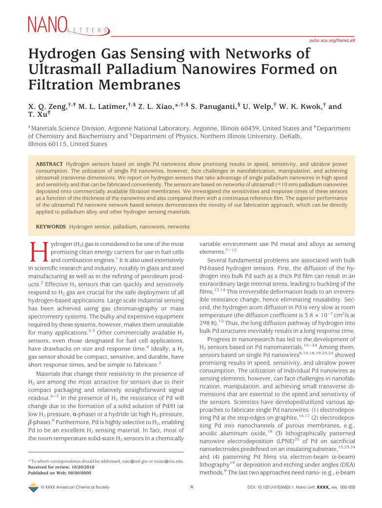
Porous Anodisc inorganic membranes from Whatmanhave been widely used as filters in chemistry. The straightnanochannels in the bulk of the membranes have also beenutilized as templates to grow nanowires18,26,27 and nano-tubes.20 Though the available nominal effective filtrationpore diameters are 20, 50, 100, and 200 nm, on the surface,the diameter of the nanochannels in the bulk of the mem-brane is unchanged (i.e., 200 nm).27 The effective filtrationof the membranes with pore diameter smaller than 200 nmisdeterminedbytheporediametersofaverythin(∼300-400nm) layer of a nanoporous network array supported on topof a 60 µm thick membrane containing vertical nanochan-nels 200 nm in diameter, as shown by the cross-sectionmicrograph given in inset of Figure 1a. For a nominaleffective filtration pore diameter of 20 nm, the materialsections between neighboring pores is less than 10 nm wide(please see Figure 4b in ref 27 for a micrograph on thesurface of a bare membrane). We utilized these sections asa template to form a wire network array of Pd by depositingPd onto it.
Anodisc 13 membranes with a nominal filtration porediameter of 20 nm were purchased from Whatman Com-pany.23 They were cleaned with acetone in a ultrasonic bathfor 10 min and rinsed with deionized water followed byethanol and dried with high-purity nitrogen gas. With thefiltration layer facing the Pd target, we sputtered Pd onto thefilter surface of the membrane using an ATC-2400 thin filmdeposition system with a base vacuum of ∼1 × 10⁻⁷ Torr.Argon was used as the working gas at a pressure of 3 mTorr.
A deposition rate of 1.3 Å/s determined by an in situ quartzcrystal microbalance (QCM) thickness monitor (model TM-350 from Maxtek, Inc.) was used to calculate the sputteringtime for a desired nominal thickness of the deposited Pd.The final products were imaged with a high-resolution fieldemission scanning electron microscope (SEM) (Hitachi S-4700II). A rectangle-shaped sample was cut out from the Pd-coated membrane and mounted onto a sample holder withfour silver pads. Electrical connections were made from thesilver pads to a current source (Keithly 6221) and to a digitalto analog (DAC) board (NI6259) via a voltage preamplifier(SR560). Silver paste was used to attach the wires to thesilver pads. Standard four-contact resistive measurementswere carried out at a constant current mode with currentranging from tens of nanoamperes to a few milliamperes,depending on the sample resistance. The inset to Figure 1bshows an optical image of the device with the Pd-coated sidefacing up. A homemade hydrogen sensor testing systemusing a series of ultrafast solenoid valves and a minimizeddead volume of the gas passages was used to accurately
FIGURE 1. Scanning electron microscopy (SEM) micrographs ofnetworks of Pd nanowires. The nominal thickness of the depositedPd is 7 nm (a) and 30 nm (b), respectively. Inset to (a) is a cross-section SEM micrograph of an Anodisc 13 membrane with filtrationpore diameter of 20 nm. The part between the two red dashed linesis the effective filtration layer. The black scale bar in the inset is400 nm. Inset to (b) presents an optical image of a sample cut outfrom the Pd-coated membrane mounted on a sample holder.
© XXXX American Chemical Society B DOI: 10.1021/nl103682s | Nano Lett. XXXX, xxx, 000-–000
characterize these sensors with response times down to tensof milliseconds.21 H2 gas (Airgas, ultrahigh purity) waspremixed with N2 gas (Airgas, ultrahigh purity) to a desiredconcentration using flow controllers (Aalborg GFC17A). Wereplaced the pure H2 with certified 1% or 0.1% H2 balancedin N2 to achieve H2 concentration at parts per million levels.N2 was also used as the purging gas. The total gas flow ratewas 200 sccm. All the tests were conducted at roomtemperature.
Figure 1 presents top-view SEM micrographs of Anodisc13 membranes with pore diameter of 20 nm after depositedPd with nominal thicknesses of 7 and 30 nm, respectively.By comparing Figure 1a to Figure 4b in ref 27, one finds thatthe morphology of the membrane does not change signifi-cantly after coating with 7 nm thick Pd. With increasingthickness of the deposited Pd, however, the pores shrink andthe widths of the Pd sections between neighboring poresbecome larger, as can be seen from the micrograph pre-sented in Figure 1b. Quantitatively, the widths of the Pdnanowires (i.e., sections between the pores) in panels a andb of Figure 1 are 7-9 and 12-15 nm, respectively. Thoughwe did not carry out detailed investigations on the relation-ship between the width of the Pd nanowires and the nominalthickness of the deposited Pd, it is reasonable to estimatethat their widths are close to the widths of the sectionsbetween pores in the bare templates and their thickness isthat of the deposited Pd if its nominal thickness is less than10 nm. This relation is more complicated with thickerdeposited Pd. We find that wire networks with deposited Pdless than 10 nm are more promising as sensors. Those withthicker deposited Pd were also studied for comparison.
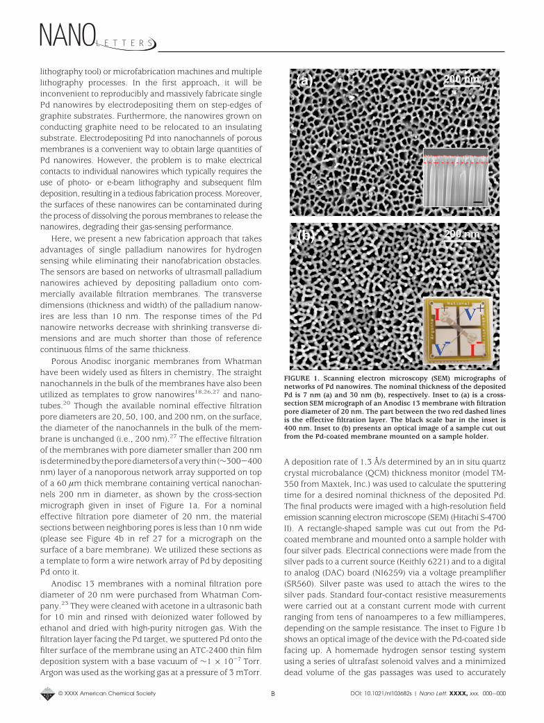
A plot of the time dependence of the resistance for a 7nm thick Pd nanowire network at various H2 concentrationsis shown in Figure 2. In the presence of hydrogen gas theresistance of the sample increases with time and saturatesat a value that depends on the gas concentration. The insetto Figure 2 demonstrates the concentration dependence ofthe maximal resistance change ∆RM/R0 and the responsetime which is defined as the rise time to reach 90% of itsmaximal change. The results are similar to those reportedfor electrodeposited nanowires15 where ∆RM/R0 first in-creases with H2 concentration up to about 3% and thenremains constant at higher concentrations. Furthermore,quantitative analysis demonstrates that the concentrationdependence of the maximal resistance change follows apower-law relation with an exponent of 0.58 for concentra-tions up to 3%. This indicates that the interaction of H2 andPd in this concentration range follows Sievert’s law.28 Thatis, the ratio of the dissolved atomic hydrogen to Pd atomscan be described to a good approximation with a power-law dependence of the hydrogen partial pressure (i.e., H2
gas concentrations in our experiments) and the change ofthis ratio leads to a proportional ∆RM/R0 response.28 Theexponent of 0.58 is slightly larger than those (∼0.4-0.50)reported in the literature for Pd films.14,28 However, as
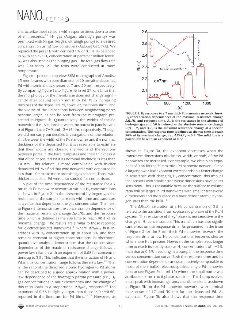
shown in Figure 3a, the exponent decreases when thetransverse dimensions (thickness, width, or both) of the Pdnanowires are increased. For example, we obtain an expo-nent of 0.46 for the 30 nm thick Pd nanowire network. Sincea larger power-law exponent corresponds to a faster changein resistance with changing H2 concentration, this impliesthat sensors with smaller transverse dimensions have bettersensitivity. This is reasonable because the surface to volumeratio will be larger in Pd nanowires with smaller transversedimensions and the surface can have denser atomic hydro-gen sites than the bulk.18
The ∆RM/R0 saturation at a H2 concentration of 3% isrelated to the transition from R-phase to -phase of the Pd/Hsystem. The resistance of the -phase is not sensitive to thechange in H2 concentration. This transition has also signifi-cant effect on the response time. As presented in the insetof Figure 2 for the 7 nm thick Pd nanowire network, theresponse time at low H2 concentrations becomes shorterwhen more H2 is present. However, the sample needs longertime to reach its steady state at H2 concentrations of 1-3%than that at 0.5%, resulting in a bump in the response timeversus concentration curve. Both the response time and itsconcentration dependence are quantitatively comparable tothose of the smallest electrodeposited single Pd nanowire(please see Figure 7e in ref 15) where the small bump wasattributed to the R- to -phase transition. This bump evolvesinto a peak with increasing transverse dimensions, as shownin Figure 3b for the Pd nanowire networks with nominalthicknesses of 17 and 30 nm for the deposited Pd. Asexpected, Figure 3b also shows that the response time
FIGURE 2. H2 response to a 7 nm thick Pd nanowire network. Inset:H2 concentration dependences of the maximal resistance change∆RM/R0 and response time. R0 is the resistance in the absence ofhydrogen gas and ∆R is defined as the absolute resistance changeR(t) - R0 and ∆RM is the maximal resistance change at a specificconcentration. The response time is defined as the rise time to reach90% of its maximal change, i.e., ∆R/∆RM ) 0.9. The solid line is apower-law fit with an exponent of 0.58.
© XXXX American Chemical Society C DOI: 10.1021/nl103682s | Nano Lett. XXXX, xxx, 000-–000
becomes longer at all H2 concentrations for samples withthicker Pd nanowires.
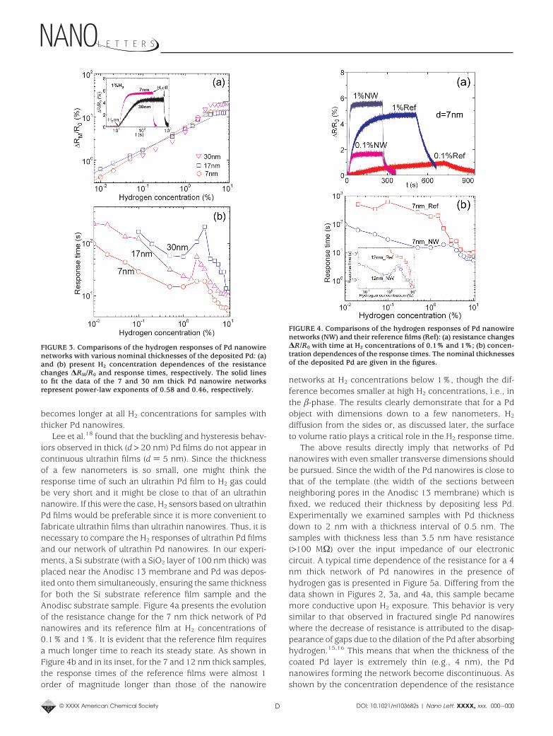
Lee et al.18 found that the buckling and hysteresis behav-iors observed in thick (d > 20 nm) Pd films do not appear incontinuous ultrathin films (d ) 5 nm). Since the thicknessof a few nanometers is so small, one might think theresponse time of such an ultrathin Pd film to H2 gas couldbe very short and it might be close to that of an ultrathinnanowire. If this were the case, H2 sensors based on ultrathinPd films would be preferable since it is more convenient tofabricate ultrathin films than ultrathin nanowires. Thus, it isnecessary to compare the H2 responses of ultrathin Pd filmsand our network of ultrathin Pd nanowires. In our experi-ments, a Si substrate (with a SiO2 layer of 100 nm thick) wasplaced near the Anodisc 13 membrane and Pd was depos-ited onto them simultaneously, ensuring the same thicknessfor both the Si substrate reference film sample and theAnodisc substrate sample. Figure 4a presents the evolutionof the resistance change for the 7 nm thick network of Pdnanowires and its reference film at H2 concentrations of0.1% and 1%. It is evident that the reference film requiresa much longer time to reach its steady state. As shown inFigure 4b and in its inset, for the 7 and 12 nm thick samples,the response times of the reference films were almost 1order of magnitude longer than those of the nanowire
networks at H2 concentrations below 1%, though the dif-ference becomes smaller at high H2 concentrations, i.e., inthe -phase. The results clearly demonstrate that for a Pdobject with dimensions down to a few nanometers, H2
diffusion from the sides or, as discussed later, the surfaceto volume ratio plays a critical role in the H2 response time.
The above results directly imply that networks of Pdnanowires with even smaller transverse dimensions shouldbe pursued. Since the width of the Pd nanowires is close tothat of the template (the width of the sections betweenneighboring pores in the Anodisc 13 membrane) which isfixed, we reduced their thickness by depositing less Pd.Experimentally we examined samples with Pd thicknessdown to 2 nm with a thickness interval of 0.5 nm. Thesamples with thickness less than 3.5 nm have resistance(>100 MΩ) over the input impedance of our electroniccircuit. A typical time dependence of the resistance for a 4nm thick network of Pd nanowires in the presence ofhydrogen gas is presented in Figure 5a. Differing from thedata shown in Figures 2, 3a, and 4a, this sample becamemore conductive upon H2 exposure. This behavior is verysimilar to that observed in fractured single Pd nanowireswhere the decrease of resistance is attributed to the disap-pearance of gaps due to the dilation of the Pd after absorbinghydrogen.15,16 This means that when the thickness of thecoated Pd layer is extremely thin (e.g., 4 nm), the Pdnanowires forming the network become discontinuous. Asshown by the concentration dependence of the resistance
FIGURE 3. Comparisons of the hydrogen responses of Pd nanowirenetworks with various nominal thicknesses of the deposited Pd: (a)and (b) present H2 concentration dependences of the resistancechanges ∆RM/R0 and response times, respectively. The solid linesto fit the data of the 7 and 30 nm thick Pd nanowire networksrepresent power-law exponents of 0.58 and 0.46, respectively.
FIGURE 4. Comparisons of the hydrogen responses of Pd nanowirenetworks (NW) and their reference films (Ref): (a) resistance changes∆R/R0 with time at H2 concentrations of 0.1% and 1%; (b) concen-tration dependences of the response times. The nominal thicknessesof the deposited Pd are given in the figures.
© XXXX American Chemical Society D DOI: 10.1021/nl103682s | Nano Lett. XXXX, xxx, 000-–000
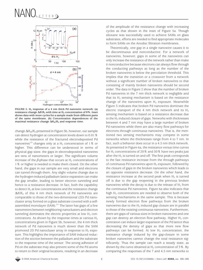
change ∆RM/R0 presented in Figure 5b, however, our samplecan detect hydrogen at concentration levels down to 0.01%while the resistance of the fractured electrodeposited Pdnanowires15 changes only at a H2 concentration of 1% orhigher. This difference can be understood in terms ofphysical gap sizes: the gaps in electrodeposited nanowiresare tens of nanometers or larger. The significant volumeincrease of the -phase that occurs at H2 concentrations of1% or higher is needed to make them closed. On the otherhand, the gaps in our sample are very small and electronscan tunnel through them. Any slight volume change due tothe hydrogen-induced palladium lattice expansion can makethe gap smaller, leading to better electron tunneling andhence to a resistance decrease. In fact, both the capabilityto detect H2 at low concentrations and the resistance change∆R/R0 of this 4 nm thick network of Pd nanowires arecomparable to those of the two-dimensional (2D) Pd nano-cluster array formed on a glass substrate covered with a self-assembled monolayer (SAM).21 The latter has gaps of a fewnanometers between neighboring nanoclusters and electrontunneling dominates the electric properties at low H2 con-centrations. As shown by the response times at various H2
concentrations given in Figure 5b, however, the 4 nm thicknetwork of Pd nanowires is much slower than the SAMpromoted 2D Pd nanocluser array in response to H2 expo-sure. This highlights the importance of SAM induced reduc-tion of the stiction between the palladium and the substrateto the response time of the sensor. The strong adhesion ofPd on the substrate may also prevent some of the Pd atomsto return to their original locations, resulting in an decrease
of the amplitude of the resistance change with increasingcycles as that shown in the inset of Figure 5a. Thoughsiloxane was successfully used to achieve SAMs on glasssubstrates, efforts are needed to find appropriate moleculesto form SAMs on the Anodisc filtration membranes.
Theoretically, one gap in a single nanowire causes it tobe discontinuous and nonconductive. For a network ofnanowires, however, gaps in some of the nanowires canonly increase the resistance of the network rather than makeit nonconductive because electrons can always flow throughthe conducting pathways as long as the number of thebroken nanowires is below the percolation threshold. Thisimplies that the transition or a crossover from a networkwithout a significant number of broken nanowires to thatconsisting of mainly broken nanowires should be secondorder. The data in Figure 2 show that the number of brokenPd nanowires in the 7 nm thick network is negligible andthat its H2 sensing mechanism is based on the resistancechange of the nanowires upon H2 exposure. MeanwhileFigure 5 indicates that broken Pd nanowires dominate theelectric transport of the 4 nm thick network and its H2
sensing mechanism is based on a resistance decrease dueto the H2 induced closure of gaps. Networks with thicknessesbetween 4 and 7 nm may have a large number of brokenPd nanowires while there are also many flow pathways forelectrons through continuous nanowires. That is, the men-tioned two sensing mechanisms may compete in somenetworks where the thicknesses range from 4 to 7 nm. Infact, such a behavior does occur in a 4.5 nm thick network.As presented in Figure 6a, the resistance versus time curvesfor H2 concentrations of 20% and 50% have two peaks justafter the H2 is turned on and off. The first peak correspondsto the fast resistance increase from the through pathwaysof continuous Pd nanowires upon H2 exposure, followed bythe closure of gaps in the broken nanowires which leads toan opposite resistance decrease. On the other hand, theresistance increase at the second peak when H2 is turnedoff is due to the gap reopening in the previous brokennanowires while the decay is due to the release of H2 fromthe continuous Pd nanowires. Figure 6a also indicates thathigh H2 concentrations are needed to observe both of thesensing mechanisms in the same sample. This is becausenewly formed electron flow pathways from the brokennanowires due to the H2 induced gap closure are in parallelto those of the existing continuous nanowires. Furthermore,there are gaps of various sizes in broken nanowires and onegap can destroy an electron flow pathway. Higher H2 con-centration can induce larger expansion of the Pd lattice thusdecreasing the density of gaps so that more new flowpathways can be formed. At low H2 concentration, theresistance change induced by the gap-closure in somebroken nanowires cannot change the total resistance sig-nificantly. Thus the sample can reach a steady state, asshown by the curve obtained at H2 concentration of 3%. Bycomparing the responses of the 7 and 4.5 nm networks to
FIGURE 5. H2 response of a 4 nm thick Pd nanowire network: (a)resistance change ∆R/R0 with time at H2 concentration of 8%. Insetshows data with more cycles for a sample made from different partsof the same membrane. (b) Concentration dependences of themaximal resistance change ∆RM/R0 and response time.
© XXXX American Chemical Society E DOI: 10.1021/nl103682s | Nano Lett. XXXX, xxx, 000-–000
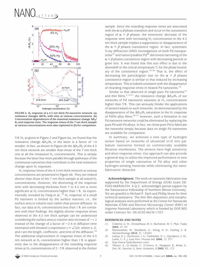
3% H2 as given in Figure 2 and Figure 6a, we found that theresistance change ∆RM/R0 in the latter is a factor of ∼4smaller. In fact, as shown in Figure 6b the ∆RM/R0 of the 4.5nm thick network are smaller than those of the 7 nm thickone at all the measured H2 concentrations. This is simplybecause the latter has more parallel through-pathways of thecontinuous nanowires that contribute to the total resistancechange upon H2 exposure.
H2 response times of the 4.5 nm thick network at variousconcentrations are presented in Figure 6b. They are indeedshorter than those of the 7 nm thick sample at all tested H2
concentrations. However, the shortening of the responsetime with decreasing thickness from 7 to 4.5 nm is moresignificant at H2 concentrations higher than 1%. As experi-mentally revealed by Fang et al.,24 H2 response of a smallPd nanowire is limited by the surface reaction, i.e., thesurface area to volume ratio rather than proton diffusion. Infact, our data at H2 concentrations less than 1% are consis-tent with their findings: the slightly shorter response timesobserved in the 4.5 nm thick sample can be understoodconsidering the surface area to volume ratio increase of ∼1.2instead of the change of a factor of ∼2.4 in diffusion timeestimated with Einstein’s expression x )2Dt, where x, D,and t are the length, coefficient, and time of the diffusion.24
The additional improvement in response times of the 4.5nm network at H2 concentration higher than 1% is appar-ently due to the disappearance of the retarding responsetimes at H2 concentrations of 2-3% observed in the thicker
sample. Since the retarding response times are associatedwith the R to phase transition and occur in the coexistenceregion of R + phases, the monotonic decrease of theresponse time with increasing H2 concentration in the 4.5nm thick sample implies a suppression or disappearance ofthe R + phases coexistence region. In fact, systematicX-ray diffraction (XRD) investigations on both Pd nanopar-ticles29 and nanocrystalline Pd30 did reveal narrowing of theR+ phases coexistence region with decreasing particle orgrain size. It was found that this size effect is due to thedownshift in the critical temperature Tc for the phase bound-ary of the coexistence region.29,30 That is, the effect ofdecreasing the particle/grain size on the R + phasescoexistence region is similar to that induced by increasingtemperature. This is indeed consistent with the disappreanceof retarding response times in heated Pd nanowires.23
Similar to that observed in single pure Pd nanowires15
and thin films,2,14,21 the resistance change ∆RM/R0 of ournetworks of Pd nanowires saturates at H2 concentrationshigher than 3%. This can seriously hinder the applicationsof sensors based on such networks. As demonstrated by thedisappearance of the ∆RM/R0 saturation in the H2 responseof Pd/Ni alloy films;28,31 however, such a limitation in ourPd nanowire networks could be eliminated by replacing thepure Pd with Pd alloys. In fact, we chose pure Pd to fabricatethe networks simply because data on single Pd nanowiresare available for comparison.
In summary, we achieved a new type of hydrogensensor based on networks of ultrasmall (<10 nm) pal-ladium nanowires formed on commercially availablefiltration membranes. The sensors have high sensitivityand short response times. Our approach can also providea general way to utilize the improved performance or newproperties of single nanowires of Pd alloy and otherhydrogen-sensing materials while eliminating the nano-fabrication obstacles.
Acknowledgment. The work on nanowire fabrication wassupported by the Department of Energy (DOE) Grant DE-FG02-06ER46334. X.Q.Z. acknowledges partial support bythe Nanoscience Fellowship of Northern Illinois University.We are grateful to Michael P. Zach and Phillip Stone for theirtechnical assistance. The thin film deposition and morpho-logical analyses were performed at the Center for NanoscaleMaterials (CNM) and Electron Microscopy Center (EMC) ofArgonne National Laboratory which is funded by DOE BESunder Contract No. DE-AC02-06CH11357.
REFERENCES AND NOTES(1) Crabtree, G. W.; Dresselhaus, M. S.; Buchanan, M. V. Phys. Today
2004, 57, 39.(2) Ramanathan, M.; Skudlarek, G.; Wang, H. H.; Darling, S. B.
Nanotechnology 2010, 21, 125501.(3) Liekus, K. J.; Zlochower, I. A.; Cashdollar, K. L.; Djordjevic, S. M.;
Loehr, C. A. J. Loss Prev. Process Ind. 2000, 13, 377.(4) http://www.fuelcellsensor.com/.(5) Tibuzzi, A.; Di Natale, C.; D’Amico, A.; Margesin, B.; Brida, S.;
Zen, M.; Soncini, G. Sens. Actuators, B 2002, 83, 175.
FIGURE 6. H2 response of a 4.5 nm thick Pd nanowire network: (a)resistance changes ∆R/R0 with time at various concentrations. (b)Concentration dependences of the maximal resistance change ∆RM/R0 and response time. The response times of the 7 nm thick sampleat various concentrations were also replotted in (b) for comparison.
© XXXX American Chemical Society F DOI: 10.1021/nl103682s | Nano Lett. XXXX, xxx, 000-–000
(6) Kong, J.; Chapline, M. G.; Dai, H. J. Adv. Mater. 2001, 13, 1384.(7) Bodzenta, J.; Burak, B.; Gacek, Z.; Jakubik, W. P.; Kochowski, S.;
Urbanczyk, M. Sens. Actuators, B 2002, 87, 82.(8) Offermans, P.; Tong, H. D.; van Rijn, C. J. M.; Merken, P.;
Brongersma, S. H.; Crego-Calama, M. Appl. Phys. Lett. 2009, 94,223110.
(9) For a nice review, please see: Christofides, C.; Mandelis, A. J. Appl.Phys. 1990, 68, R1.
(10) Chen, H.-I.; Chou, Y.-I.; Chu, C.-Y. Sens. Actuators, B 2002, 85,10.
(11) Wang, C.; Mandelis, A.; Garcia, J. A. Rev. Sci. Instrum. 1999, 70,4370.
(12) Sutapun, B.; Tabib-Azar, M.; Kazemi, A. Sens. Actuators, B 1999,60, 27.
(13) Pundt, A. Adv. Eng. Mater. 2004, 6, 11.(14) Lee, E.; Lee, J. M.; Koo, J. H.; Lee, W.; Lee, T. Int. J. Hydrogen
Energy 2010, 35, 6984.(15) Yang, F.; Taggart, D. K.; Penner, R. M. Nano Lett. 2009, 9, 2177.(16) Favier, F.; Walter, E. C.; Zach, M. P.; Benter, T.; M. Penner, R. M.
Science 2001, 293, 2227.(17) Walter, E. C.; Favier, F.; Penner, R. M. Anal. Chem. 2002, 74, 1546.(18) Jeon, K. J.; Jeun, M.; Lee, E.; Lee, J. M.; Lee, K. I.; von Allmen, P.;
Lee, W. Nanotechnology 2009, 19, 495501.(19) Jeon, K. J.; Lee, J. M.; Lee, E.; Lee, W. Nanotechnology 2009, 20,
135502.
(20) Yu, S. F.; Welp, U.; Hua, L. Z.; Rydh, A.; Kwok, W. K.; Wang, H. H.Chem. Mater. 2005, 17, 3445.
(21) Xu, T.; Zach, M. P.; Xiao, Z. L.; Rosenmann, D.; Welp, U.; Kwok,W. K.; Crabtree, G. W. Appl. Phys. Lett. 2005, 86, 203104.
(22) Khanuja, M.; Kala, S.; Mehta, B. R.; Kruis, F. E. Nanotechnology2009, 20, 015502.
(23) Yang, F.; Taggart, D. K.; Penner, R. M. Small 2010, 6, 1422.(24) Yang, F.; Kung, S.-C.; Cheng, M.; Hemminger, J. C.; Penner, R. M.
ACS Nano 2010, 4, 5233.(25) Menke, E. J.; Thompson, M. A.; Xiang, C.; Yang, L. C.; Penner,
R. M. Nat. Mater. 2006, 5, 914.(26) http://www.whatman.com/PRODAnoporeInorganicMembranes.
aspx.(27) Xiao, Z. L.; Han, C. Y.; Welp, U.; Wang, H. H.; Kwok, W. K.;
Willing, G. A.; Hiller, J. M.; Cook, R. E.; Miller, D. J.; Crabtree, G. W.Nano Lett. 2002, 2, 1293, and references therein.
(28) Thomas, R. C.; Hughes, R. C. J. Electrochem. Soc. 1997, 144, 3245.(29) Narehood, D. G.; Kishore, S.; Goto, H.; Adair, J. H.; Nelson, J. A.;
Gutierrez, H. R.; Eklund, P. C. Int. J. Hydrogen Energy 2009, 34,952.
(30) Eastman, J. A.; Thompson, L. J.; Kestel, B. J. Phys. Rev. B 1993,48, 84.
(31) Hughes, R. C.; Schubert, W. K. J. Appl. Phys. 1992, 71, 542.
© XXXX American Chemical Society G DOI: 10.1021/nl103682s | Nano Lett. XXXX, xxx, 000-–000


![Palladium nanoparticles and nanowires deposited ... - Pd-JSSE.pdf · processes such as catalysis, fuel cells, hydrogen storage and metal embrittlement [22]. Research on palladium](https://static.fdocuments.net/doc/165x107/5f0236a27e708231d403233a/palladium-nanoparticles-and-nanowires-deposited-pd-jssepdf-processes-such.jpg)