HSPICE Quick Reference Guide - Chalmersperla/ugrad/EDA351/HSPICEQuickRef.pdf · HSPICE Quick...
86
HSPICE Quick Reference Guide ® U-2003.03, March 2003 Comments? E-mail your comments about Synopsys documentation to [email protected]
Transcript of HSPICE Quick Reference Guide - Chalmersperla/ugrad/EDA351/HSPICEQuickRef.pdf · HSPICE Quick...

HSPICEQuick Reference Guide
®
U-2003.03, March 2003
Comments?
E-mail your comments about Synopsys documentation to [email protected]

Copyright Notice and Proprietary InformationCopyright 2003 Synopsys, Inc. All rights reserved. This software and documentation contain confidential and proprietary information that is the property of Synopsys, Inc. The software and documentation are furnished under a license agreement and may be used or copied only in accordance with the terms of the license agreement. No part of the software and documentation may be reproduced, transmitted, or translated, in any form or by any means, electronic, mechanical, manual, optical, or otherwise, without prior written permission of Synopsys, Inc., or as expressly provided by the license agreement.
Right to Copy DocumentationThe license agreement with Synopsys permits licensee to make copies of the documentation for its internal use only. Each copy shall include all copyrights, trademarks, service marks, and proprietary rights notices, if any. Licensee must assign sequential numbers to all copies. These copies shall contain the following legend on the cover page:“This document is duplicated with the permission of Synopsys, Inc., for the exclusive use of __________________________________________ and its employees. This is copy number __________.”
Destination Control StatementAll technical data contained in this publication is subject to the export control laws of the United States of America. Disclosure to nationals of other countries contrary to United States law is prohibited. It is the reader’s responsibility to determine the applicable regulations and to comply with them.
DisclaimerSYNOPSYS, INC., AND ITS LICENSORS MAKE NO WARRANTY OF ANY KIND, EXPRESS OR IMPLIED, WITH REGARD TO THIS MATERIAL, INCLUDING, BUT NOT LIMITED TO, THE IMPLIED WARRANTIES OF MERCHANTABILITY AND FITNESS FOR A PARTICULAR PURPOSE.
Registered Trademarks (®)Synopsys, AMPS, Arcadia, C Level Design, C2HDL, C2V, C2VHDL, Calaveras Algorithm, CoCentric, COSSAP, CSim, DelayMill, DesignPower, DesignWare, Device Model Builder, Enterprise, EPIC, Formality, HSPICE, Hypermodel, I, InSpecs, in-Sync, LEDA, MAST, Meta, Meta-Software, ModelAccess, ModelExpress, ModelTools, PathBlazer, PathMill, PowerArc, PowerMill, PrimeTime, RailMill, Raphael, RapidScript, Saber, SmartLogic, SNUG, SolvNet, Stream Driven Simulator, Superlog, System Compiler, TestBench Manager, Testify, TetraMAX, TimeMill, TMA, VERA, VeriasHDL, and WaveCalc are registered trademarks of Synopsys, Inc.
Trademarks (™)Active Parasitics, AFGen, Apollo, Apollo II, Apollo-DPII, Apollo-GA, ApolloGAII, Astro, Astro-Rail, Astro-Xtalk, Aurora, AvanTestchip, AvanWaves, BCView, Behavioral Compiler, BOA, BRT, Cedar, ChipPlanner, Circuit Analysis, Columbia, Columbia-CE, Comet 3D, Cosmos, Cosmos SE, CosmosLE, Cosmos-Scope, Cyclelink, Davinci, DC Expert, DC Expert Plus, DC Professional, DC Ultra, DC Ultra Plus, Design Advisor, Design Analyzer, Design Compiler, DesignerHDL, DesignTime, DFM-Workbench, DFT Compiler SoCBIST, Direct RTL, Direct Silicon Access, DW8051, DWPCI, Dynamic-Macromodeling, Dynamic Model Switcher, ECL Compiler, ECO Compiler, EDAnavigator, Encore, Encore PQ, Evaccess, ExpressModel, Floorplan Manager, Formal Model Checker, FormalVera, FoundryModel, FPGA Compiler II, FPGA Express, Frame Compiler, Frameway, Gatran, HDL Advisor, HDL Compiler, Hercules, Hercules-Explorer, Hercules-II, Hierarchical Optimization Technology, High Performance Option, HotPlace, HSPICE-Link, Integrator, Interactive Waveform Viewer, iQBus, Jupiter, Jupiter-DP, JupiterXT, JupiterXT-ASIC, JVXtreme, Liberty, Libra-Passport, Library Compiler, Libra-Visa, LRC, Mars, Mars-Rail, Mars-Xtalk, Medici, Metacapture, Metacircuit, Metamanager, Metamixsim, Milkyway, ModelSource, Module Compiler, MS-3200, MS-3400, NanoSim, Nova Product Family, Nova-ExploreRTL, Nova-Trans, Nova-VeriLint, Nova-VHDLlint, OpenVera, Optimum Silicon, Orion_ec, Parasitic View, Passport, Physical Compiler, Planet, Planet-PL, Planet-RTL, Polaris, Polaris-CBS, Polaris-MT, Power Compiler, PowerCODE, PowerGate, ProFPGA, Progen, Prospector, Proteus OPC, Protocol Compiler, PSMGen, Raphael-NES, RoadRunner, RTL Analyzer, Saber Co-Simulation, Saber for IC Design, SaberDesigner, SaberGuide, SaberRT, SaberScope, SaberSketch, Saturn, ScanBand, Schematic Compiler, Scirocco, Scirocco-i, Shadow Debugger, Silicon Blueprint, Silicon Early Access, SinglePass-SoC, Smart Extraction, SmartLicense, SmartModel Library, Softwire, Source-Level Design, Star, Star-DC, Star-Hspice, Star-HspiceLink, Star-MS, Star-MTB, Star-Power, Star-Rail, Star-RC, Star-RCXT, Star-Sim, Star-Sim XT, Star-Time, Star-XP, SWIFT, Taurus, Taurus-Device, Taurus-Layout, Taurus-Lithography, Taurus-OPC, Taurus-Process, Taurus-Topography, Taurus-Visual, Taurus-Workbench, Test Compiler, TestGen, TetraMAX TenX, The Power in Semiconductors, TheHDL, TimeSlice, TimeTracker, Timing Annotator, TopoPlace, TopoRoute, Trace-On-Demand, True-Hspice, TSUPREM-4, TymeWare, VCS, VCS Express, VCSi, Venus, Verification Portal, VFormal, VHDL Compiler, VHDL System Simulator, VirSim, and VMC are trademarks of Synopsys, Inc.
Service Marks (SM)DesignSphere, SVP Café, and TAP-in are service marks of Synopsys, Inc.
SystemC is a trademark of the Open SystemC Initiative and is used under license.All other product or company names may be trademarks of their respective owners.Printed in the U.S.A.
Document Order Number: 37919-000 PAHSPICE Quick Reference Guide, U-2003.03
HSPICE Quick Reference GuideTable of Contents
Introduction 1
Input and Output Files 2
Behavior Macromodeling 6
Controlling Input 18
Analyzing Data 41
Optimizing Data 56
Output Format 59

IntroductionThis Quick Reference Guide is a condensed version of the HSPICE Simulation and Analysis User Guide and the HSPICE Applications Manual. For more specific details and examples refer to the relevant manual.
Syntax Notation
The meaning of a parameter may depend on its location in the statement. Be sure that a complete set of parameters is entered in the correct sequence before running the simulation.
Common Abbreviations
xxx, yyy, zzz Arbitrary alphanumeric strings
< ... > Optional data fields are enclosed in angle brackets < >. All other symbols and punctuation are required.
UPPERCASE Keywords, parameter names, etc. are represented in uppercase.
lowercase Variables; should be replaced with a numeric or symbolic value.
... Any number of parameters of the form shown can be entered.
+ Continuation of the preceding line.
Å Angstrom
amp ampere
cm centimeter
deg degree Centigrade (unless specified as Kelvin)
ev electron volt
F farad
H Henry
m meter
s second
V volt
Introduction 1
2
Input and Output Files
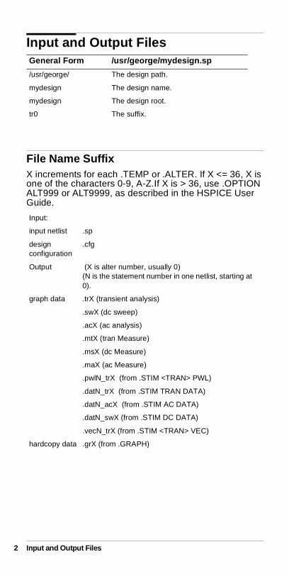
File Name SuffixX increments for each .TEMP or .ALTER. If X <= 36, X is one of the characters 0-9, A-Z.If X is > 36, use .OPTION ALT999 or ALT9999, as described in the HSPICE User Guide.
General Form /usr/george/mydesign.sp
/usr/george/ The design path.
mydesign The design name.
mydesign The design root.
tr0 The suffix.
Input:
input netlist .sp
design configuration
.cfg
Output (X is alter number, usually 0)(N is the statement number in one netlist, starting at 0).
graph data .trX (transient analysis)
.swX (dc sweep)
.acX (ac analysis)
.mtX (tran Measure)
.msX (dc Measure)
.maX (ac Measure)
.pwlN_trX (from .STIM <TRAN> PWL)
.datN_trX (from .STIM TRAN DATA)
.datN_acX (from .STIM AC DATA)
.datN_swX (from .STIM DC DATA)
.vecN_trX (from .STIM <TRAN> VEC)
hardcopy data .grX (from .GRAPH)
Input and Output Files
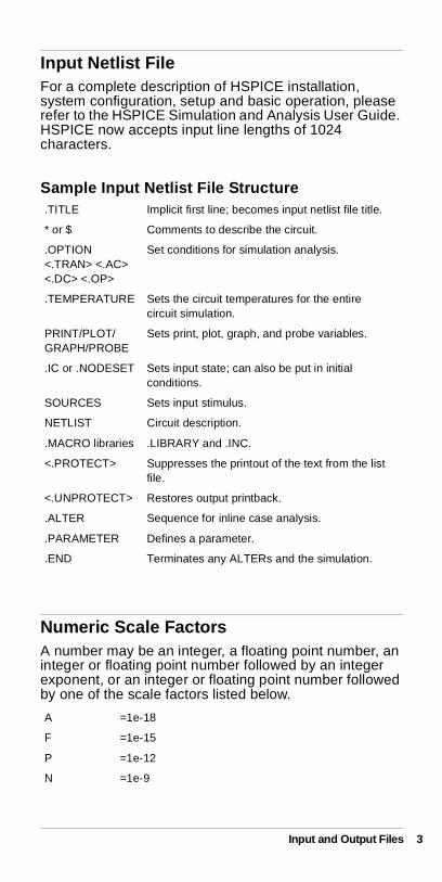
Input Netlist FileFor a complete description of HSPICE installation, system configuration, setup and basic operation, please refer to the HSPICE Simulation and Analysis User Guide. HSPICE now accepts input line lengths of 1024 characters.
Sample Input Netlist File Structure
Numeric Scale FactorsA number may be an integer, a floating point number, an integer or floating point number followed by an integer exponent, or an integer or floating point number followed by one of the scale factors listed below.
.TITLE Implicit first line; becomes input netlist file title.
* or $ Comments to describe the circuit.
.OPTION <.TRAN> <.AC> <.DC> <.OP>
Set conditions for simulation analysis.
.TEMPERATURE Sets the circuit temperatures for the entire circuit simulation.
PRINT/PLOT/GRAPH/PROBE
Sets print, plot, graph, and probe variables.
.IC or .NODESET Sets input state; can also be put in initial conditions.
SOURCES Sets input stimulus.
NETLIST Circuit description.
.MACRO libraries .LIBRARY and .INC.
<.PROTECT> Suppresses the printout of the text from the list file.
<.UNPROTECT> Restores output printback.
.ALTER Sequence for inline case analysis.
.PARAMETER Defines a parameter.
.END Terminates any ALTERs and the simulation.
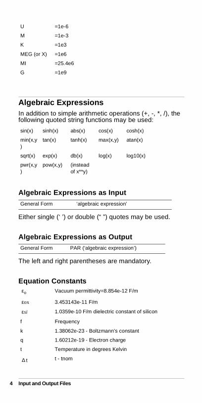
A =1e-18
F =1e-15
P =1e-12
N =1e-9
Input and Output Files 3
4
Algebraic ExpressionsIn addition to simple arithmetic operations (+, -, *, /), the following quoted string functions may be used:
Algebraic Expressions as Input
Either single (‘ ’) or double (“ ”) quotes may be used.
Algebraic Expressions as Output
The left and right parentheses are mandatory.
Equation Constants
U =1e-6
M =1e-3
K =1e3
MEG (or X) =1e6
MI =25.4e6
G =1e9
sin(x) sinh(x) abs(x) cos(x) cosh(x)
min(x,y)
tan(x) tanh(x) max(x,y) atan(x)
sqrt(x) exp(x) db(x) log(x) log10(x)
pwr(x,y)
pow(x,y) (instead of x**y)
General Form ‘algebraic expression’
General Form PAR (‘algebraic expression’)
Vacuum permittivity=8.854e-12 F/m
3.453143e-11 F/m
1.0359e-10 F/m dielectric constant of silicon
f Frequency
k 1.38062e-23 - Boltzmann’s constant
q 1.60212e-19 - Electron charge
t Temperature in degrees Kelvin
t t - tnom
εo
εox
εsi
∆
Input and Output Files
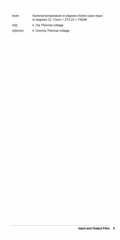
tnom Nominal temperature in degrees Kelvin (user-input in degrees C). Tnom = 273.15 + TNOM
vt(t) k ⋅ t/q Thermal voltage
vt(tnom) k ⋅ tnom/q Thermal voltage
Input and Output Files 5
6
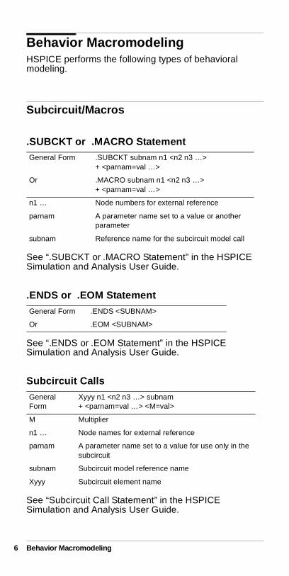
Behavior MacromodelingHSPICE performs the following types of behavioral modeling.
Subcircuit/Macros
.SUBCKT or .MACRO Statement
See “.SUBCKT or .MACRO Statement” in the HSPICE Simulation and Analysis User Guide.
.ENDS or .EOM Statement
See “.ENDS or .EOM Statement” in the HSPICE Simulation and Analysis User Guide.
Subcircuit Calls
See “Subcircuit Call Statement” in the HSPICE Simulation and Analysis User Guide.
General Form .SUBCKT subnam n1 <n2 n3 …>+ <parnam=val …>
Or .MACRO subnam n1 <n2 n3 …>+ <parnam=val …>
n1 … Node numbers for external reference
parnam A parameter name set to a value or another parameter
subnam Reference name for the subcircuit model call
General Form .ENDS <SUBNAM>
Or .EOM <SUBNAM>
General Form
Xyyy n1 <n2 n3 …> subnam + <parnam=val …> <M=val>
M Multiplier
n1 … Node names for external reference
parnam A parameter name set to a value for use only in the subcircuit
subnam Subcircuit model reference name
Xyyy Subcircuit element name
Behavior Macromodeling
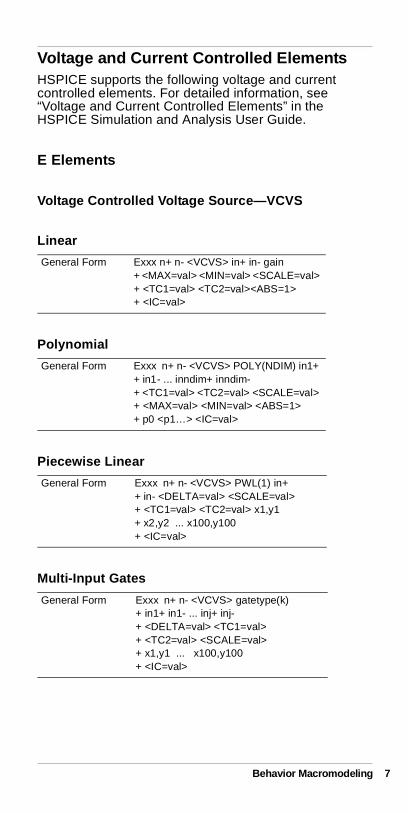
Voltage and Current Controlled ElementsHSPICE supports the following voltage and current controlled elements. For detailed information, see “Voltage and Current Controlled Elements” in the HSPICE Simulation and Analysis User Guide.
E Elements
Voltage Controlled Voltage Source—VCVS
Linear
Polynomial
Piecewise Linear
Multi-Input Gates
General Form Exxx n+ n- <VCVS> in+ in- gain + <MAX=val> <MIN=val> <SCALE=val> + <TC1=val> <TC2=val><ABS=1> + <IC=val>
General Form Exxx n+ n- <VCVS> POLY(NDIM) in1+ + in1- ... inndim+ inndim-+ <TC1=val> <TC2=val> <SCALE=val> + <MAX=val> <MIN=val> <ABS=1>+ p0 <p1…> <IC=val>
General Form Exxx n+ n- <VCVS> PWL(1) in+ + in- <DELTA=val> <SCALE=val> + <TC1=val> <TC2=val> x1,y1 + x2,y2 ... x100,y100 + <IC=val>
General Form Exxx n+ n- <VCVS> gatetype(k) + in1+ in1- ... inj+ inj- + <DELTA=val> <TC1=val> + <TC2=val> <SCALE=val> + x1,y1 ... x100,y100 + <IC=val>
Behavior Macromodeling 7
8
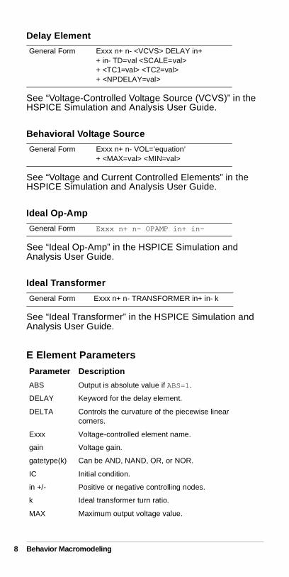
Delay Element
See “Voltage-Controlled Voltage Source (VCVS)” in the HSPICE Simulation and Analysis User Guide.
Behavioral Voltage Source
See “Voltage and Current Controlled Elements” in the HSPICE Simulation and Analysis User Guide.
Ideal Op-Amp
See “Ideal Op-Amp” in the HSPICE Simulation and Analysis User Guide.
Ideal Transformer
See “Ideal Transformer” in the HSPICE Simulation and Analysis User Guide.
E Element Parameters
General Form Exxx n+ n- <VCVS> DELAY in+ + in- TD=val <SCALE=val> + <TC1=val> <TC2=val> + <NPDELAY=val>
General Form Exxx n+ n- VOL=’equation’ + <MAX=val> <MIN=val>
General Form Exxx n+ n- OPAMP in+ in-
General Form Exxx n+ n- TRANSFORMER in+ in- k
Parameter Description
ABS Output is absolute value if ABS=1.
DELAY Keyword for the delay element.
DELTA Controls the curvature of the piecewise linear corners.
Exxx Voltage-controlled element name.
gain Voltage gain.
gatetype(k) Can be AND, NAND, OR, or NOR.
IC Initial condition.
in +/- Positive or negative controlling nodes.
k Ideal transformer turn ratio.
MAX Maximum output voltage value.
Behavior Macromodeling
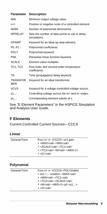
See “E Element Parameters” in the HSPICE Simulation and Analysis User Guide.
F ElementsCurrent Controlled Current Sources—CCCS
Linear
Polynomial
MIN Minimum output voltage value.
n+/- Positive or negative node of a controlled element.
NDIM Number of polynomial dimensions.
NPDELAY Sets the number of data points to use in delay simulations.
OPAMP Keyword for an ideal op-amp element.
P0, P1… Polynomial coefficients.
POLY Polynomial keyword.
PWL Piecewise linear function keyword.
SCALE Element value multiplier.
TC1, TC2 First-order and second-order temperature coefficients.
TD Time (propagation) delay keyword.
TRANSFORMER
Keyword for an ideal transformer.
VCVS Keyword for a voltage-controlled voltage source.
x1,… Controlling voltage across the in+ and in- nodes.
y1,… Corresponding element values of x.
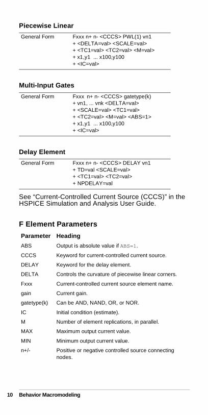
General Form Fxxx n+ n- <CCCS> vn1 gain + <MAX=val> <MIN=val> + <SCALE=val> <TC1=val> + <TC2=val> <M=val> <ABS=1> + <IC=val>
General Form Fxxx n+ n- <CCCS> POLY(ndim) + vn1 <... vnndim> <MAX=val> + <MIN=val> <TC1=val> + <TC2=val> <SCALE=val> + <M=val> <ABS=1> p0 <p1…> + <IC=val>
Parameter Description
Behavior Macromodeling 9
10
Piecewise Linear
Multi-Input Gates
Delay Element
See “Current-Controlled Current Source (CCCS)” in the HSPICE Simulation and Analysis User Guide.
F Element Parameters
General Form Fxxx n+ n- <CCCS> PWL(1) vn1 + <DELTA=val> <SCALE=val>+ <TC1=val> <TC2=val> <M=val> + x1,y1 ... x100,y100 + <IC=val>
General Form Fxxx n+ n- <CCCS> gatetype(k) + vn1, ... vnk <DELTA=val> + <SCALE=val> <TC1=val> + <TC2=val> <M=val> <ABS=1> + x1,y1 ... x100,y100 + <IC=val>
General Form Fxxx n+ n- <CCCS> DELAY vn1 + TD=val <SCALE=val> + <TC1=val> <TC2=val> + NPDELAY=val
Parameter Heading
ABS Output is absolute value if ABS=1.
CCCS Keyword for current-controlled current source.
DELAY Keyword for the delay element.
DELTA Controls the curvature of piecewise linear corners.
Fxxx Current-controlled current source element name.
gain Current gain.
gatetype(k) Can be AND, NAND, OR, or NOR.
IC Initial condition (estimate).
M Number of element replications, in parallel.
MAX Maximum output current value.
MIN Minimum output current value.
n+/- Positive or negative controlled source connecting nodes.
Behavior Macromodeling
See “F Element Parameters” in the HSPICE Simulation and Analysis User Guide.
G Elements
Voltage Controlled Current Source—VCCS
Linear
Polynomial
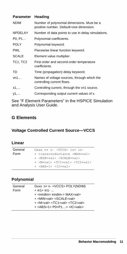
NDIM Number of polynomial dimensions. Must be a positive number. Default=one dimension.
NPDELAY Number of data points to use in delay simulations.
P0, P1… Polynomial coefficients.
POLY Polynomial keyword.
PWL Piecewise linear function keyword.
SCALE Element value multiplier.
TC1, TC2 First-order and second-order temperature coefficients.
TD Time (propagation) delay keyword.
vn1… Names of voltage sources, through which the controlling current flows.
x1,… Controlling current, through the vn1 source.
y1,… Corresponding output current values of x.
General Form
Gxxx n+ n- <VCCS> in+ in- + transconductance <MAX=val> + <MIN=val> <SCALE=val> + <M=val> <TC1=val> <TC2=val> + <ABS=1> <IC=val>
General Form
Gxxx n+ n- <VCCS> POLY(NDIM) + in1+ in1- ... + <inndim+ inndim-> MAX=val> + <MIN=val> <SCALE=val> + <M=val> <TC1=val> <TC2=val> + <ABS=1> P0<P1…> <IC=vals>
Parameter Heading
Behavior Macromodeling 11
12
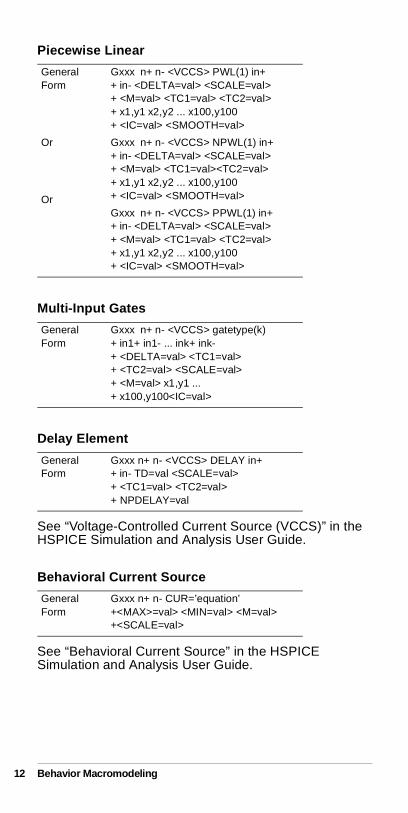
Piecewise Linear
Multi-Input Gates
Delay Element
See “Voltage-Controlled Current Source (VCCS)” in the HSPICE Simulation and Analysis User Guide.
Behavioral Current Source
See “Behavioral Current Source” in the HSPICE Simulation and Analysis User Guide.
General Form
Or
Or
Gxxx n+ n- <VCCS> PWL(1) in+ + in- <DELTA=val> <SCALE=val> + <M=val> <TC1=val> <TC2=val> + x1,y1 x2,y2 ... x100,y100 + <IC=val> <SMOOTH=val>
Gxxx n+ n- <VCCS> NPWL(1) in++ in- <DELTA=val> <SCALE=val> + <M=val> <TC1=val><TC2=val> + x1,y1 x2,y2 ... x100,y100 + <IC=val> <SMOOTH=val>
Gxxx n+ n- <VCCS> PPWL(1) in++ in- <DELTA=val> <SCALE=val> + <M=val> <TC1=val> <TC2=val> + x1,y1 x2,y2 ... x100,y100 + <IC=val> <SMOOTH=val>
General Form
Gxxx n+ n- <VCCS> gatetype(k) + in1+ in1- ... ink+ ink- + <DELTA=val> <TC1=val> + <TC2=val> <SCALE=val> + <M=val> x1,y1 ... + x100,y100<IC=val>
General Form
Gxxx n+ n- <VCCS> DELAY in++ in- TD=val <SCALE=val> + <TC1=val> <TC2=val>+ NPDELAY=val
General Form
Gxxx n+ n- CUR=’equation’ +<MAX>=val> <MIN=val> <M=val> +<SCALE=val>
Behavior Macromodeling
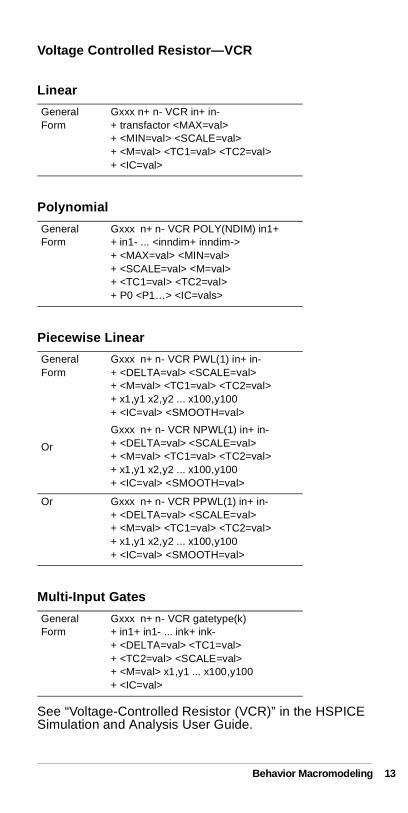
Voltage Controlled Resistor—VCR
Linear
Polynomial
Piecewise Linear
Multi-Input Gates
See “Voltage-Controlled Resistor (VCR)” in the HSPICE Simulation and Analysis User Guide.
General Form
Gxxx n+ n- VCR in+ in- + transfactor <MAX=val> + <MIN=val> <SCALE=val> + <M=val> <TC1=val> <TC2=val> + <IC=val>
General Form
Gxxx n+ n- VCR POLY(NDIM) in1+ + in1- ... <inndim+ inndim-> + <MAX=val> <MIN=val> + <SCALE=val> <M=val> + <TC1=val> <TC2=val> + P0 <P1…> <IC=vals>
General Form
Or
Gxxx n+ n- VCR PWL(1) in+ in- + <DELTA=val> <SCALE=val> + <M=val> <TC1=val> <TC2=val>+ x1,y1 x2,y2 ... x100,y100 + <IC=val> <SMOOTH=val>
Gxxx n+ n- VCR NPWL(1) in+ in-+ <DELTA=val> <SCALE=val> + <M=val> <TC1=val> <TC2=val> + x1,y1 x2,y2 ... x100,y100 + <IC=val> <SMOOTH=val>
Or Gxxx n+ n- VCR PPWL(1) in+ in- + <DELTA=val> <SCALE=val> + <M=val> <TC1=val> <TC2=val> + x1,y1 x2,y2 ... x100,y100 + <IC=val> <SMOOTH=val>
General Form
Gxxx n+ n- VCR gatetype(k) + in1+ in1- ... ink+ ink- + <DELTA=val> <TC1=val> + <TC2=val> <SCALE=val> + <M=val> x1,y1 ... x100,y100 + <IC=val>
Behavior Macromodeling 13
14
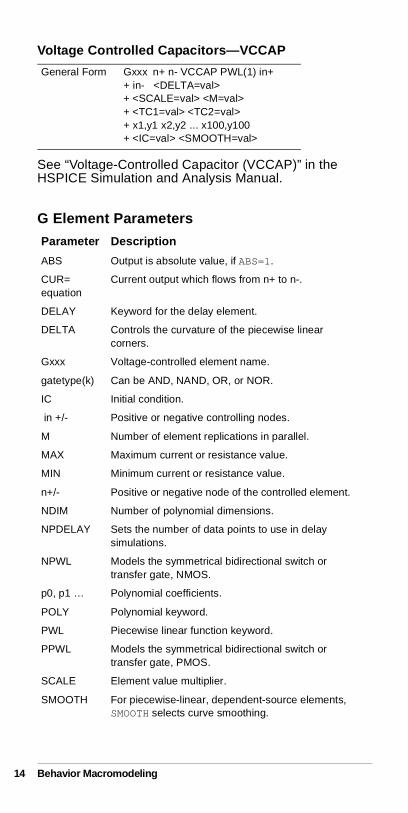
Voltage Controlled Capacitors—VCCAP
See “Voltage-Controlled Capacitor (VCCAP)” in the HSPICE Simulation and Analysis Manual.
G Element Parameters
General Form Gxxx n+ n- VCCAP PWL(1) in+ + in- <DELTA=val> + <SCALE=val> <M=val> + <TC1=val> <TC2=val> + x1,y1 x2,y2 ... x100,y100 + <IC=val> <SMOOTH=val>
Parameter Description
ABS Output is absolute value, if ABS=1.
CUR= equation
Current output which flows from n+ to n-.
DELAY Keyword for the delay element.
DELTA Controls the curvature of the piecewise linear corners.
Gxxx Voltage-controlled element name.
gatetype(k) Can be AND, NAND, OR, or NOR.
IC Initial condition.
in +/- Positive or negative controlling nodes.
M Number of element replications in parallel.
MAX Maximum current or resistance value.
MIN Minimum current or resistance value.
n+/- Positive or negative node of the controlled element.
NDIM Number of polynomial dimensions.
NPDELAY Sets the number of data points to use in delay simulations.
NPWL Models the symmetrical bidirectional switch or transfer gate, NMOS.
p0, p1 … Polynomial coefficients.
POLY Polynomial keyword.
PWL Piecewise linear function keyword.
PPWL Models the symmetrical bidirectional switch or transfer gate, PMOS.
SCALE Element value multiplier.
SMOOTH For piecewise-linear, dependent-source elements, SMOOTH selects curve smoothing.
Behavior Macromodeling
See “G Element Parameters” in the HSPICE Simulation and Analysis User Guide.
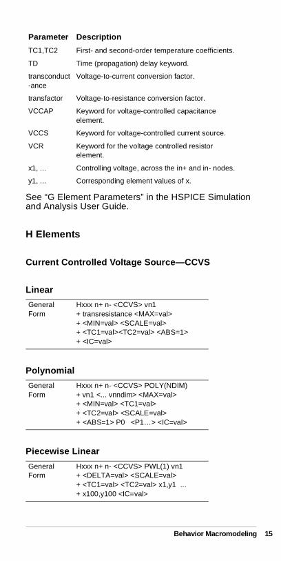
H Elements
Current Controlled Voltage Source—CCVS
Linear
Polynomial
Piecewise Linear
TC1,TC2 First- and second-order temperature coefficients.
TD Time (propagation) delay keyword.
transconduct-ance
Voltage-to-current conversion factor.
transfactor Voltage-to-resistance conversion factor.
VCCAP Keyword for voltage-controlled capacitance element.
VCCS Keyword for voltage-controlled current source.
VCR Keyword for the voltage controlled resistor element.
x1, ... Controlling voltage, across the in+ and in- nodes.
y1, ... Corresponding element values of x.
General Form
Hxxx n+ n- <CCVS> vn1 + transresistance <MAX=val> + <MIN=val> <SCALE=val> + <TC1=val><TC2=val> <ABS=1> + <IC=val>
General Form
Hxxx n+ n- <CCVS> POLY(NDIM) + vn1 <... vnndim> <MAX=val> + <MIN=val> <TC1=val> + <TC2=val> <SCALE=val> + <ABS=1> P0 <P1…> <IC=val>
General Form
Hxxx n+ n- <CCVS> PWL(1) vn1+ <DELTA=val> <SCALE=val>+ <TC1=val> <TC2=val> x1,y1 ... + x100,y100 <IC=val>
Parameter Description
Behavior Macromodeling 15
16
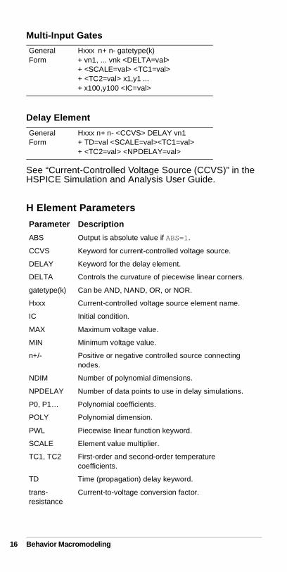
Multi-Input Gates
Delay Element
See “Current-Controlled Voltage Source (CCVS)” in the HSPICE Simulation and Analysis User Guide.
H Element Parameters
General Form
Hxxx n+ n- gatetype(k) + vn1, ... vnk <DELTA=val> + <SCALE=val> <TC1=val> + <TC2=val> x1,y1 ... + x100,y100 <IC=val>
General Form
Hxxx n+ n- <CCVS> DELAY vn1 + TD=val <SCALE=val><TC1=val> + <TC2=val> <NPDELAY=val>
Parameter Description
ABS Output is absolute value if ABS=1.
CCVS Keyword for current-controlled voltage source.
DELAY Keyword for the delay element.
DELTA Controls the curvature of piecewise linear corners.
gatetype(k) Can be AND, NAND, OR, or NOR.
Hxxx Current-controlled voltage source element name.
IC Initial condition.
MAX Maximum voltage value.
MIN Minimum voltage value.
n+/- Positive or negative controlled source connecting nodes.
NDIM Number of polynomial dimensions.
NPDELAY Number of data points to use in delay simulations.
P0, P1… Polynomial coefficients.
POLY Polynomial dimension.
PWL Piecewise linear function keyword.
SCALE Element value multiplier.
TC1, TC2 First-order and second-order temperature coefficients.
TD Time (propagation) delay keyword.
trans-resistance
Current-to-voltage conversion factor.
Behavior Macromodeling
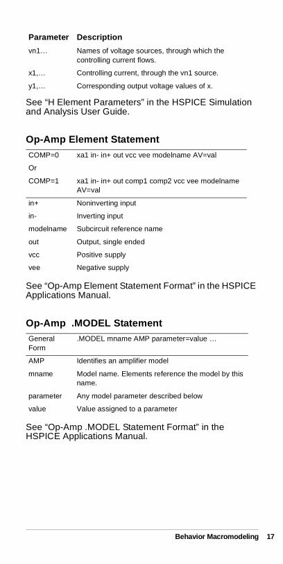
See “H Element Parameters” in the HSPICE Simulation and Analysis User Guide.
Op-Amp Element Statement
See “Op-Amp Element Statement Format” in the HSPICE Applications Manual.
Op-Amp .MODEL Statement
See “Op-Amp .MODEL Statement Format” in the HSPICE Applications Manual.
vn1… Names of voltage sources, through which the controlling current flows.
x1,… Controlling current, through the vn1 source.
y1,… Corresponding output voltage values of x.
COMP=0 xa1 in- in+ out vcc vee modelname AV=val
Or
COMP=1 xa1 in- in+ out comp1 comp2 vcc vee modelname AV=val
in+ Noninverting input
in- Inverting input
modelname Subcircuit reference name
out Output, single ended
vcc Positive supply
vee Negative supply
General Form
.MODEL mname AMP parameter=value …
AMP Identifies an amplifier model
mname Model name. Elements reference the model by this name.
parameter Any model parameter described below
value Value assigned to a parameter
Parameter Description
Behavior Macromodeling 17
18
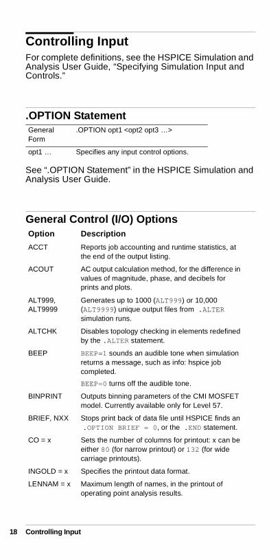
Controlling InputFor complete definitions, see the HSPICE Simulation and Analysis User Guide, “Specifying Simulation Input and Controls.”
.OPTION Statement
See “.OPTION Statement” in the HSPICE Simulation and Analysis User Guide.
General Control (I/O) Options
General Form
.OPTION opt1 <opt2 opt3 …>
opt1 … Specifies any input control options.
Option Description
ACCT Reports job accounting and runtime statistics, at the end of the output listing.
ACOUT AC output calculation method, for the difference in values of magnitude, phase, and decibels for prints and plots.
ALT999, ALT9999
Generates up to 1000 (ALT999) or 10,000 (ALT9999) unique output files from .ALTER simulation runs.
ALTCHK Disables topology checking in elements redefined by the .ALTER statement.
BEEP BEEP=1 sounds an audible tone when simulation returns a message, such as info: hspice job completed.
BEEP=0 turns off the audible tone.
BINPRINT Outputs binning parameters of the CMI MOSFET model. Currently available only for Level 57.
BRIEF, NXX Stops print back of data file until HSPICE finds an .OPTION BRIEF = 0, or the .END statement.
CO = x Sets the number of columns for printout: x can be either 80 (for narrow printout) or 132 (for wide carriage printouts).
INGOLD = x Specifies the printout data format.
LENNAM = x Maximum length of names, in the printout of operating point analysis results.
Controlling Input
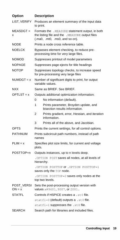
LIST, VERIFY Produces an element summary of the input data to print.
MEASDGT =x
Formats the .MEASURE statement output, in both the listing file and the .MEASURE output files (.ma0, .mt0, .ms0, and so on).
NODE Prints a node cross reference table.
NOELCK Bypasses element checking, to reduce pre-processing time for very large files.
NOMOD Suppresses printout of model parameters
NOPAGE Suppresses page ejects for title headings
NOTOP Suppresses topology checks, to increase speed for pre-processing very large files
NUMDGT = x Number of significant digits to print, for output variable values.
NXX Same as BRIEF. See BRIEF.
OPTLST = x Outputs additional optimization information:
0 No information (default).
1 Prints parameter, Broyden update, andbisection results information.
2 Prints gradient, error, Hessian, and iterationinformation.
3 Prints all of the above, and Jacobian.
OPTS Prints the current settings, for all control options.
PATHNUM Prints subcircuit path numbers, instead of path names
PLIM = x Specifies plot size limits, for current and voltage plots.
POSTTOP=n Outputs instances, up to n levels deep.
.OPTION POST saves all nodes, at all levels of hierarchy.
.OPTION POSTTOP or .OPTION POSTTOP=1 saves only the TOP node.
.OPTION POSTTOP=2 saves only nodes at the top two levels.
POST_VERSION = x
Sets the post-processing output version with values x=9601, 9007, or 2001..
STATFL Controls if HSPICE creates a .st0 file.
statfl=0 (default) outputs a .st0 file.
statfl=1 suppresses the .st0 file.
SEARCH Search path for libraries and included files.
Option Description
Controlling Input 19

20
See “General Control Options” in the HSPICE Simulation and Analysis User Guide.
IBIS PKG and EDB Simulation Input
See “Using PKG and EBD Simulation” in the HSPICE User Guide.
CPU Options
See “CPU Options” in the HSPICE Simulation and Analysis User Guide.
VERIFY Same as LIST. See LIST.
Option Description
EBDMAP Name of a map file, which lists the relationship between HSPICE sub-circuit names and:
IBIS board-level module.
X element name in the sub-circuit.
On-board component.
EBDTYPE Type of elements to use, to represent board-level pin connected traces.
PKGMAP: Name of EBD map file. This file lists the relationship between the HSPICE subcircuit and the IBIS component.
PKGTYPE Types of elements to use, to represent the package effect.
Option Description
CPTIME = x Maximum CPU time, in seconds, allotted for this simulation job.
EPSMIN = x Smallest number that a computer can add or subtract, a constant value.
EXPMAX = x Largest exponent that you can use for an exponential, before overflow occurs.
LIMTIM = x Amount of CPU time reserved to generate prints and plots, if a CPU time limit (CPTIME = x) terminates simulation.
Option Description
Controlling Input
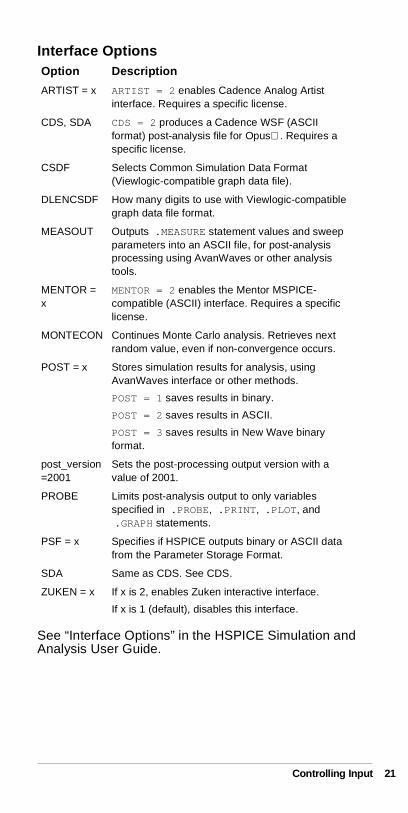
Interface Options
See “Interface Options” in the HSPICE Simulation and Analysis User Guide.
Option Description
ARTIST = x ARTIST = 2 enables Cadence Analog Artist interface. Requires a specific license.
CDS, SDA CDS = 2 produces a Cadence WSF (ASCII format) post-analysis file for Opus . Requires a specific license.
CSDF Selects Common Simulation Data Format (Viewlogic-compatible graph data file).
DLENCSDF How many digits to use with Viewlogic-compatible graph data file format.
MEASOUT Outputs .MEASURE statement values and sweep parameters into an ASCII file, for post-analysis processing using AvanWaves or other analysis tools.
MENTOR =x
MENTOR = 2 enables the Mentor MSPICE-compatible (ASCII) interface. Requires a specific license.
MONTECON Continues Monte Carlo analysis. Retrieves next random value, even if non-convergence occurs.
POST = x Stores simulation results for analysis, using AvanWaves interface or other methods.
POST = 1 saves results in binary.
POST = 2 saves results in ASCII.
POST = 3 saves results in New Wave binary format.
post_version=2001
Sets the post-processing output version with a value of 2001.
PROBE Limits post-analysis output to only variables specified in .PROBE, .PRINT, .PLOT, and .GRAPH statements.
PSF = x Specifies if HSPICE outputs binary or ASCII data from the Parameter Storage Format.
SDA Same as CDS. See CDS.
ZUKEN = x If x is 2, enables Zuken interactive interface.
If x is 1 (default), disables this interface.
Controlling Input 21
22
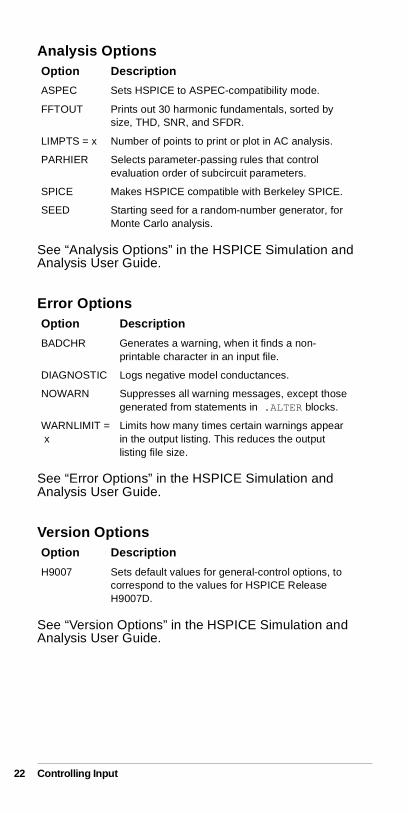
Analysis Options
See “Analysis Options” in the HSPICE Simulation and Analysis User Guide.
Error Options
See “Error Options” in the HSPICE Simulation and Analysis User Guide.
Version Options
See “Version Options” in the HSPICE Simulation and Analysis User Guide.
Option Description
ASPEC Sets HSPICE to ASPEC-compatibility mode.
FFTOUT Prints out 30 harmonic fundamentals, sorted by size, THD, SNR, and SFDR.
LIMPTS = x Number of points to print or plot in AC analysis.
PARHIER Selects parameter-passing rules that control evaluation order of subcircuit parameters.
SPICE Makes HSPICE compatible with Berkeley SPICE.
SEED Starting seed for a random-number generator, for Monte Carlo analysis.
Option Description
BADCHR Generates a warning, when it finds a non-printable character in an input file.
DIAGNOSTIC Logs negative model conductances.
NOWARN Suppresses all warning messages, except those generated from statements in .ALTER blocks.
WARNLIMIT =x
Limits how many times certain warnings appear in the output listing. This reduces the output listing file size.
Option Description
H9007 Sets default values for general-control options, to correspond to the values for HSPICE Release H9007D.
Controlling Input
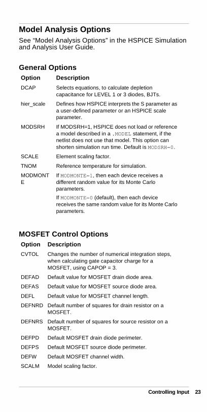
Model Analysis OptionsSee “Model Analysis Options” in the HSPICE Simulation and Analysis User Guide.
General Options
MOSFET Control Options
Option Description
DCAP Selects equations, to calculate depletion capacitance for LEVEL 1 or 3 diodes, BJTs.
hier_scale Defines how HSPICE interprets the S parameter as a user-defined parameter or an HSPICE scale parameter.
MODSRH If MODSRH=1, HSPICE does not load or reference a model described in a .MODEL statement, if the netlist does not use that model. This option can shorten simulation run time. Default is MODSRH=0.
SCALE Element scaling factor.
TNOM Reference temperature for simulation.
MODMONTE
If MODMONTE=1, then each device receives a different random value for its Monte Carlo parameters.
If MODMONTE=0 (default), then each device receives the same random value for its Monte Carlo parameters.
Option Description
CVTOL Changes the number of numerical integration steps, when calculating gate capacitor charge for a MOSFET, using CAPOP = 3.
DEFAD Default value for MOSFET drain diode area.
DEFAS Default value for MOSFET source diode area.
DEFL Default value for MOSFET channel length.
DEFNRD Default number of squares for drain resistor on a MOSFET.
DEFNRS Default number of squares for source resistor on a MOSFET.
DEFPD Default MOSFET drain diode perimeter.
DEFPS Default MOSFET source diode perimeter.
DEFW Default MOSFET channel width.
SCALM Model scaling factor.
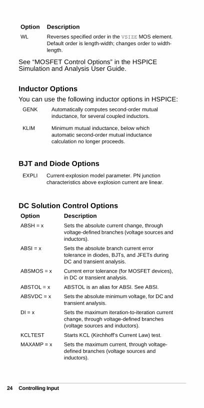
Controlling Input 23
24
See “MOSFET Control Options” in the HSPICE Simulation and Analysis User Guide.
Inductor OptionsYou can use the following inductor options in HSPICE:
BJT and Diode Options
DC Solution Control Options
WL Reverses specified order in the VSIZE MOS element. Default order is length-width; changes order to width-length.
GENK Automatically computes second-order mutual inductance, for several coupled inductors.
KLIM Minimum mutual inductance, below which automatic second-order mutual inductance calculation no longer proceeds.
EXPLI Current-explosion model parameter. PN junction characteristics above explosion current are linear.
Option Description
ABSH = x Sets the absolute current change, through voltage-defined branches (voltage sources and inductors).
ABSI = x Sets the absolute branch current error tolerance in diodes, BJTs, and JFETs during DC and transient analysis.
ABSMOS = x Current error tolerance (for MOSFET devices), in DC or transient analysis.
ABSTOL = x ABSTOL is an alias for ABSI. See ABSI.
ABSVDC = x Sets the absolute minimum voltage, for DC and transient analysis.
DI = x Sets the maximum iteration-to-iteration current change, through voltage-defined branches (voltage sources and inductors).
KCLTEST Starts KCL (Kirchhoff’s Current Law) test.
MAXAMP = x Sets the maximum current, through voltage-defined branches (voltage sources and inductors).
Option Description
Controlling Input
See “DC Operating Point, DC Sweep, and Pole/Zero Options” in the HSPICE Simulation and Analysis User Guide.
Matrix Options
Pole/Zero I/O Options
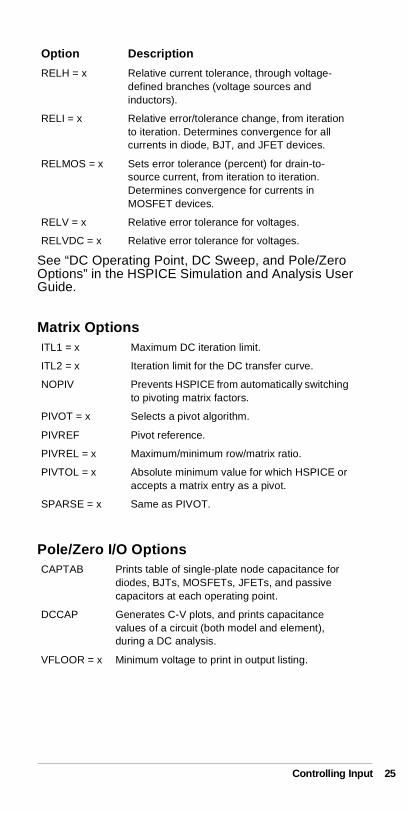
RELH = x Relative current tolerance, through voltage-defined branches (voltage sources and inductors).
RELI = x Relative error/tolerance change, from iteration to iteration. Determines convergence for all currents in diode, BJT, and JFET devices.
RELMOS = x Sets error tolerance (percent) for drain-to-source current, from iteration to iteration. Determines convergence for currents in MOSFET devices.
RELV = x Relative error tolerance for voltages.
RELVDC = x Relative error tolerance for voltages.
ITL1 = x Maximum DC iteration limit.
ITL2 = x Iteration limit for the DC transfer curve.
NOPIV Prevents HSPICE from automatically switching to pivoting matrix factors.
PIVOT = x Selects a pivot algorithm.
PIVREF Pivot reference.
PIVREL = x Maximum/minimum row/matrix ratio.
PIVTOL = x Absolute minimum value for which HSPICE or accepts a matrix entry as a pivot.
SPARSE = x Same as PIVOT.
CAPTAB Prints table of single-plate node capacitance for diodes, BJTs, MOSFETs, JFETs, and passive capacitors at each operating point.
DCCAP Generates C-V plots, and prints capacitance values of a circuit (both model and element), during a DC analysis.
VFLOOR = x Minimum voltage to print in output listing.
Option Description
Controlling Input 25
26
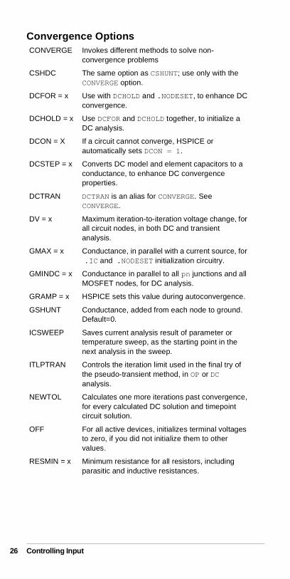
Convergence OptionsCONVERGE Invokes different methods to solve non-
convergence problems
CSHDC The same option as CSHUNT; use only with the CONVERGE option.
DCFOR = x Use with DCHOLD and .NODESET, to enhance DC convergence.
DCHOLD = x Use DCFOR and DCHOLD together, to initialize a DC analysis.
DCON = X If a circuit cannot converge, HSPICE or automatically sets DCON = 1.
DCSTEP = x Converts DC model and element capacitors to a conductance, to enhance DC convergence properties.
DCTRAN DCTRAN is an alias for CONVERGE. See CONVERGE.
DV = x Maximum iteration-to-iteration voltage change, for all circuit nodes, in both DC and transient analysis.
GMAX = x Conductance, in parallel with a current source, for .IC and .NODESET initialization circuitry.
GMINDC = x Conductance in parallel to all pn junctions and all MOSFET nodes, for DC analysis.
GRAMP = x HSPICE sets this value during autoconvergence.
GSHUNT Conductance, added from each node to ground. Default=0.
ICSWEEP Saves current analysis result of parameter or temperature sweep, as the starting point in the next analysis in the sweep.
ITLPTRAN Controls the iteration limit used in the final try of the pseudo-transient method, in OP or DC analysis.
NEWTOL Calculates one more iterations past convergence, for every calculated DC solution and timepoint circuit solution.
OFF For all active devices, initializes terminal voltages to zero, if you did not initialize them to other values.
RESMIN = x Minimum resistance for all resistors, including parasitic and inductive resistances.
Controlling Input
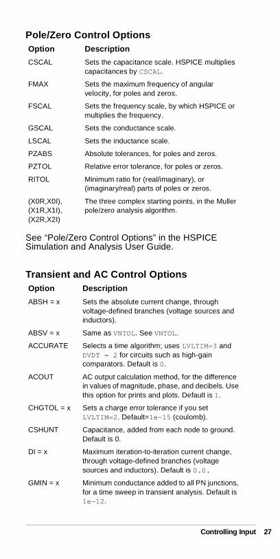
Pole/Zero Control Options
See “Pole/Zero Control Options” in the HSPICE Simulation and Analysis User Guide.
Transient and AC Control Options
Option Description
CSCAL Sets the capacitance scale. HSPICE multiplies capacitances by CSCAL.
FMAX Sets the maximum frequency of angular velocity, for poles and zeros.
FSCAL Sets the frequency scale, by which HSPICE or multiplies the frequency.
GSCAL Sets the conductance scale.
LSCAL Sets the inductance scale.
PZABS Absolute tolerances, for poles and zeros.
PZTOL Relative error tolerance, for poles or zeros.
RITOL Minimum ratio for (real/imaginary), or (imaginary/real) parts of poles or zeros.
(X0R,X0I),(X1R,X1I),(X2R,X2I)
The three complex starting points, in the Muller pole/zero analysis algorithm.
Option Description
ABSH = x Sets the absolute current change, through voltage-defined branches (voltage sources and inductors).
ABSV = x Same as VNTOL. See VNTOL.
ACCURATE Selects a time algorithm; uses LVLTIM=3 and DVDT = 2 for circuits such as high-gain comparators. Default is 0.
ACOUT AC output calculation method, for the difference in values of magnitude, phase, and decibels. Use this option for prints and plots. Default is 1.
CHGTOL = x Sets a charge error tolerance if you set LVLTIM=2. Default=1e-15 (coulomb).
CSHUNT Capacitance, added from each node to ground. Default is 0.
DI = x Maximum iteration-to-iteration current change, through voltage-defined branches (voltage sources and inductors). Default is 0.0.
GMIN = x Minimum conductance added to all PN junctions, for a time sweep in transient analysis. Default is 1e-12.
Controlling Input 27
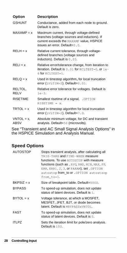
28
See “Transient and AC Small Signal Analysis Options” in the HSPICE Simulation and Analysis Manual.
Speed Options
GSHUNT Conductance, added from each node to ground. Default is zero.
MAXAMP = x Maximum current, through voltage-defined branches (voltage sources and inductors). If current exceeds the MAXAMP value, HSPICE issues an error. Default=0.0.
RELH = x Relative current tolerance, through voltage-defined branches (voltage sources and inductors). Default is 0.05.
RELI = x Relative error/tolerance change, from iteration to iteration. Default is 0.01 for KCLTEST=0, or 1e-6 for KCLTEST=1.
RELQ = x Used in timestep algorithm, for local truncation error (LVLTIM=2). Default=0.01.
RELTOL, RELV
Relative error tolerance for voltages. Default is 1e-3.
RISETIME Smallest risetime of a signal, .OPTION RISETIME = x.
TRTOL = x Used in timestep algorithm for local truncation error (LVLTIM=2). Default=7.0.
VNTOL = x, ABSV
Absolute minimum voltage, for DC and transient analysis. Default=50 (microvolts).
AUTOSTOP Stops transient analysis, after calculating all TRIG-TARG and FIND-WHEN measure functions. To use AUTOSTOP with measure functions (such as , AVG, RMS, MIN, MAX, PP, ERR, ERR1,2,3, or PARAM), set .OPTION autostop from_to or .OPTION autostsop from_to=1.
BKPSIZ = x Size of breakpoint table. Default=5000.
BYPASS To speed-up simulation, does not update status of latent devices. Default is 1.
BYTOL = x Voltage tolerance, at which a MOSFET, MESFET, JFET, BJT, or diode becomes latent. Default is MBYPASSxVNTOL.
FAST To speed-up simulation, does not update status of latent devices. Default is 0.
ITLPZ Sets the iteration limit for pole/zero analysis. Default is 100.
Option Description
Controlling Input
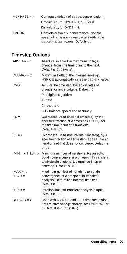
Timestep Options
MBYPASS = x Computes default of BYTOL control option.
Default is 1, for DVDT = 0, 1, 2, or 3.
Default is 2, for DVDT = 4.
TRCON Controls automatic convergence, and the speed of large non-linear circuits with large TSTOP/TSTEP values. Default=1.
ABSVAR = x Absolute limit for the maximum voltage change, from one time point to the next. Default is 0.5 (volts).
DELMAX = x Maximum Delta of the internal timestep. HSPICE automatically sets the DELMAX value.
DVDT Adjusts the timestep, based on rates of change for node voltage. Default=4.
0 - original algorithm
1 - fast
2 - accurate
3,4 - balance speed and accuracy
FS = x Decreases Delta (internal timestep) by the specified fraction of a timestep (TSTEP), for the first time point of a transient. Default=0.25.
FT = x Decreases Delta (the internal timestep), by a specified fraction of a timestep (TSTEP), for an iteration set that does not converge. Default is 0.25.
IMIN = x, ITL3 = x Minimum number of iterations. Required to obtain convergence at a timepoint in transient analysis simulations. Determines internal timestep. Default is 3.0.
IMAX = x, ITL4 = x
Maximum number of iterations to obtain convergence at a timepoint in transient analysis. Determines internal timestep. Default is 8.0.
ITL5 = x Iteration limit, for transient analysis output. Default is 0.0.
RELVAR = x Used with ABSVAR, and DVDT timestep option. Sets relative voltage change, for LVLTIM=1 or 3. Default is 0.30 (30%).
Controlling Input 29
30
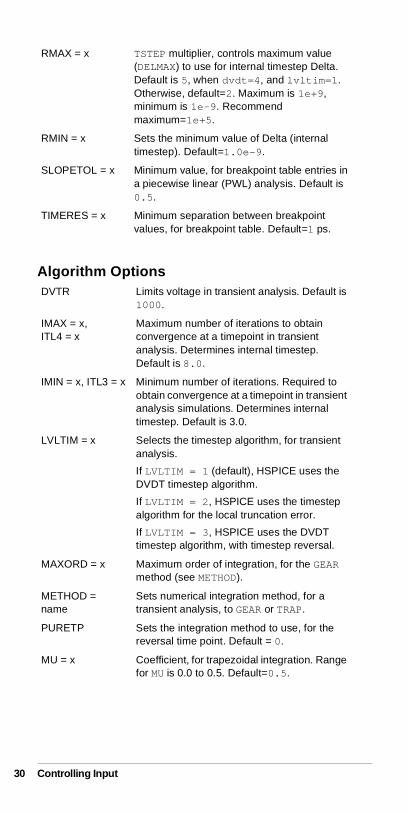
Algorithm Options
RMAX = x TSTEP multiplier, controls maximum value (DELMAX) to use for internal timestep Delta. Default is 5, when dvdt=4, and lvltim=1. Otherwise, default=2. Maximum is 1e+9, minimum is 1e-9. Recommend maximum=1e+5.
RMIN = x Sets the minimum value of Delta (internal timestep). Default=1.0e-9.
SLOPETOL = x Minimum value, for breakpoint table entries in a piecewise linear (PWL) analysis. Default is 0.5.
TIMERES = x Minimum separation between breakpoint values, for breakpoint table. Default=1 ps.
DVTR Limits voltage in transient analysis. Default is 1000.
IMAX = x, ITL4 = x
Maximum number of iterations to obtain convergence at a timepoint in transient analysis. Determines internal timestep. Default is 8.0.
IMIN = x, ITL3 = x Minimum number of iterations. Required to obtain convergence at a timepoint in transient analysis simulations. Determines internal timestep. Default is 3.0.
LVLTIM = x Selects the timestep algorithm, for transient analysis.
If LVLTIM = 1 (default), HSPICE uses the DVDT timestep algorithm.
If LVLTIM = 2, HSPICE uses the timestep algorithm for the local truncation error.
If LVLTIM = 3, HSPICE uses the DVDT timestep algorithm, with timestep reversal.
MAXORD = x Maximum order of integration, for the GEAR method (see METHOD).
METHOD =name
Sets numerical integration method, for a transient analysis, to GEAR or TRAP.
PURETP Sets the integration method to use, for the reversal time point. Default = 0.
MU = x Coefficient, for trapezoidal integration. Range for MU is 0.0 to 0.5. Default=0.5.
Controlling Input
Input and Output Options
StatementsHSPICE supports the following statements.
.ALTER Statement
See “.ALTER Statement” in the HSPICE Simulation and Analysis User Guide.
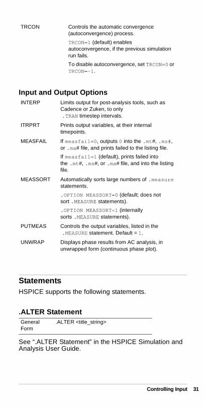
TRCON Controls the automatic convergence (autoconvergence) process.
TRCON=1 (default) enables autoconvergence, if the previous simulation run fails.
To disable autoconvergence, set TRCON=0 or TRCON=-1.
INTERP Limits output for post-analysis tools, such as Cadence or Zuken, to only.TRAN timestep intervals.
ITRPRT Prints output variables, at their internal timepoints.
MEASFAIL If measfail=0, outputs 0 into the .mt#, .ms#, or .ma# file, and prints failed to the listing file.
If measfail=1 (default), prints failed into the .mt#, .ms#, or .ma# file, and into the listing file.
MEASSORT Automatically sorts large numbers of .measure statements.
.OPTION MEASSORT=0 (default; does not sort .MEASURE statements).
.OPTION MEASSORT=1 (internally sorts .MEASURE statements).
PUTMEAS Controls the output variables, listed in the .MEASURE statement. Default = 1.
UNWRAP Displays phase results from AC analysis, in unwrapped form (continuous phase plot).
General Form
.ALTER <title_string>
Controlling Input 31
32
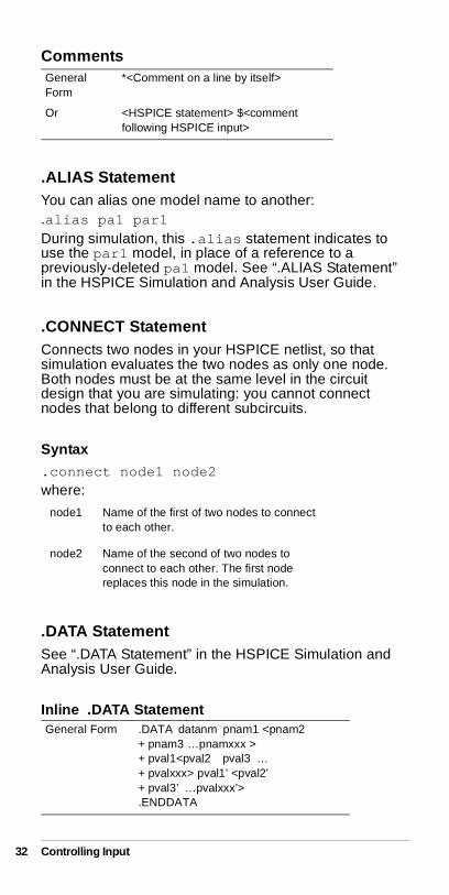
Comments
.ALIAS StatementYou can alias one model name to another:.alias pa1 par1During simulation, this .alias statement indicates to use the par1 model, in place of a reference to a previously-deleted pa1 model. See “.ALIAS Statement” in the HSPICE Simulation and Analysis User Guide.
.CONNECT StatementConnects two nodes in your HSPICE netlist, so that simulation evaluates the two nodes as only one node. Both nodes must be at the same level in the circuit design that you are simulating: you cannot connect nodes that belong to different subcircuits.
Syntax
.connect node1 node2where:
.DATA StatementSee “.DATA Statement” in the HSPICE Simulation and Analysis User Guide.
Inline .DATA Statement
General Form
*<Comment on a line by itself>
Or <HSPICE statement> $<comment following HSPICE input>
node1 Name of the first of two nodes to connect to each other.
node2 Name of the second of two nodes to connect to each other. The first node replaces this node in the simulation.
General Form .DATA datanm pnam1 <pnam2 + pnam3 …pnamxxx > + pval1<pval2 pval3 …+ pvalxxx> pval1’ <pval2’ + pval3’ …pvalxxx’>.ENDDATA
Controlling Input
External File .DATA Statement
Column Laminated .DATA Statement
See “Column Laminated .DATA Statement” in the HSPICE User Guide.
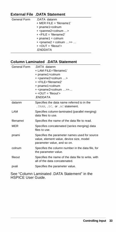
General Form .DATA datanm+ MER FILE = ‘filename1’+ pname1=colnum + <panme2=colnum …>+ <FILE = ‘filename2’ + pname1 = colnum+ <pname2 = colnum …>> …+ <OUT = ‘fileout’>.ENDDATA
General Form .DATA datanm+ LAM FILE=‘filename1’+ pname1=colnum + <panme2=colnum …>+ <FILE=‘filename2’ + pname1=colnum+ <pname2=colnum …>>…+ <OUT = ‘fileout’>.ENDDATA
datanm Specifies the data name referred to in the .TRAN, .DC, or .AC statement.
LAM Specifies column-laminated (parallel merging) data files to use.
filenamei Specifies the name of the data file to read.
MER Specifies concatenated (series merging) data files to use.
pnami Specifies the parameter names used for source value, element value, device size, model parameter value, and so on.
colnum Specifies the column number in the data file, for the parameter value.
fileout Specifies the name of the data file to write, with all of the data concatenated.
pvali Specifies the parameter value.
Controlling Input 33
34
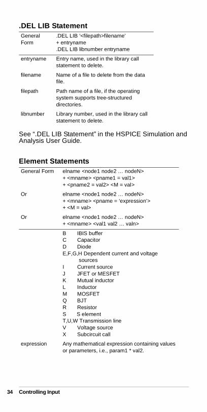
.DEL LIB Statement
See “.DEL LIB Statement” in the HSPICE Simulation and Analysis User Guide.
Element Statements
General Form
.DEL LIB ‘<filepath>filename’ + entryname.DEL LIB libnumber entryname
entryname Entry name, used in the library call statement to delete.
filename Name of a file to delete from the data file.
filepath Path name of a file, if the operating system supports tree-structured directories.
libnumber Library number, used in the library call statement to delete.
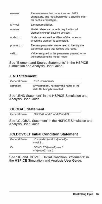
General Form elname <node1 node2 … nodeN>+ <mname> <pname1 = val1>+ <pname2 = val2> <M = val>
Or elname <node1 node2 … nodeN>+ <mname> <pname = ‘expression’>+ <M = val>
Or elname <node1 node2 … nodeN>+ <mname> <val1 val2 … valn>
B IBIS bufferC CapacitorD DiodeE,F,G,H Dependent current and voltage sourcesI Current sourceJ JFET or MESFETK Mutual inductorL InductorM MOSFETQ BJTR ResistorS S elementT,U,W Transmission lineV Voltage sourceX Subcircuit call
expression Any mathematical expression containing values or parameters, i.e., param1 * val2.
Controlling Input
See “Element and Source Statements” in the HSPICE Simulation and Analysis User Guide.
.END Statement
See “.END Statement” in the HSPICE Simulation and Analysis User Guide.
.GLOBAL Statement
See “.GLOBAL Statement” in the HSPICE Simulation and Analysis User Guide.
.IC/.DCVOLT Initial Condition Statement
See “.IC and .DCVOLT Initial Condition Statements” in the HSPICE Simulation and Analysis User Guide.
elname Element name that cannot exceed 1023 characters, and must begin with a specific letter for each element type.
M = val Element multiplier.
mname Model reference name is required for all elements except passive devices.
node1 … Node names are identifiers of the nodes to which the element is connected.
pname1 … Element parameter name used to identify the parameter value that follows this name.
val1… Value assigned to the parameter pname1 or to the corresponding model node.
General Form .END <comment>
comment Any comment, normally the name of the data file being terminated.
General Form .GLOBAL node1 node2 node3 …
General Form .IC v(node1)=val 1 v(node2)= + val 2 …
Or .DCVOLT V(node1)=val 1 + V(node2)=val 2
Controlling Input 35
36
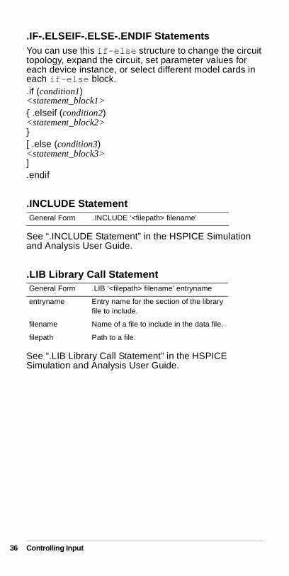
.IF-.ELSEIF-.ELSE-.ENDIF StatementsYou can use this if-else structure to change the circuit topology, expand the circuit, set parameter values for each device instance, or select different model cards in each if-else block..if (condition1)<statement_block1>{ .elseif (condition2)<statement_block2>}[ .else (condition3)<statement_block3>].endif
.INCLUDE Statement
See “.INCLUDE Statement” in the HSPICE Simulation and Analysis User Guide.
.LIB Library Call Statement
See “.LIB Library Call Statement” in the HSPICE Simulation and Analysis User Guide.
General Form .INCLUDE ‘<filepath> filename’
General Form .LIB ‘<filepath> filename’ entryname
entryname Entry name for the section of the library file to include.
filename Name of a file to include in the data file.
filepath Path to a file.
Controlling Input
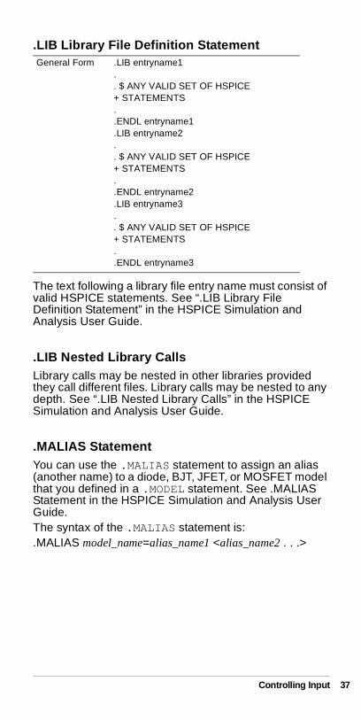
.LIB Library File Definition Statement
The text following a library file entry name must consist of valid HSPICE statements. See “.LIB Library File Definition Statement” in the HSPICE Simulation and Analysis User Guide.
.LIB Nested Library CallsLibrary calls may be nested in other libraries provided they call different files. Library calls may be nested to any depth. See “.LIB Nested Library Calls” in the HSPICE Simulation and Analysis User Guide.
.MALIAS Statement You can use the .MALIAS statement to assign an alias (another name) to a diode, BJT, JFET, or MOSFET model that you defined in a .MODEL statement. See .MALIAS Statement in the HSPICE Simulation and Analysis User Guide.The syntax of the .MALIAS statement is:.MALIAS model_name=alias_name1 <alias_name2 . . .>
General Form .LIB entryname1.. $ ANY VALID SET OF HSPICE+ STATEMENTS..ENDL entryname1.LIB entryname2.. $ ANY VALID SET OF HSPICE+ STATEMENTS..ENDL entryname2.LIB entryname3.. $ ANY VALID SET OF HSPICE+ STATEMENTS..ENDL entryname3
Controlling Input 37
38
.MODEL Statement
See “.MODEL Statement” in the HSPICE Simulation and Analysis User Guide.
.NODESET Statement
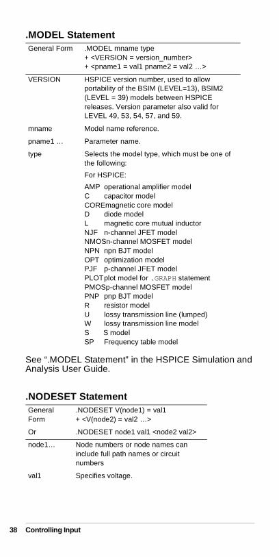
General Form .MODEL mname type+ <VERSION = version_number>+ <pname1 = val1 pname2 = val2 …>
VERSION HSPICE version number, used to allow portability of the BSIM (LEVEL=13), BSIM2 (LEVEL = 39) models between HSPICE releases. Version parameter also valid for LEVEL 49, 53, 54, 57, and 59.
mname Model name reference.
pname1 … Parameter name.
type Selects the model type, which must be one of the following:
For HSPICE:
AMP operational amplifier model C capacitor model COREmagnetic core model D diode model L magnetic core mutual inductor NJF n-channel JFET model NMOSn-channel MOSFET model NPN npn BJT model OPT optimization model PJF p-channel JFET model PLOTplot model for .GRAPH statement PMOSp-channel MOSFET model PNP pnp BJT model R resistor modelU lossy transmission line (lumped)W lossy transmission line model S S modelSP Frequency table model
General Form
.NODESET V(node1) = val1+ <V(node2) = val2 …>
Or .NODESET node1 val1 <node2 val2>
node1… Node numbers or node names can include full path names or circuit numbers
val1 Specifies voltage.
Controlling Input
See “.NODESET Statement” in the HSPICE Simulation and Analysis User Guide.
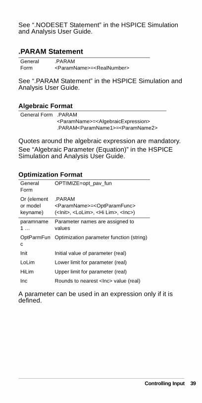
.PARAM Statement
See “.PARAM Statement” in the HSPICE Simulation and Analysis User Guide.
Algebraic Format
Quotes around the algebraic expression are mandatory.See “Algebraic Parameter (Equation)” in the HSPICE Simulation and Analysis User Guide.
Optimization Format
A parameter can be used in an expression only if it is defined.
General Form
.PARAM <ParamName>=<RealNumber>
General Form .PARAM <ParamName>=<AlgebraicExpression>.PARAM<ParamName1>=<ParamName2>
General Form
OPTIMIZE=opt_pav_fun
Or (element or model keyname)
.PARAM <ParamName>=<OptParamFunc> (<Init>, <LoLim>, <Hi Lim>, <Inc>)
paramname1 …
Parameter names are assigned to values
OptParmFunc
Optimization parameter function (string)
Init Initial value of parameter (real)
LoLim Lower limit for parameter (real)
HiLim Upper limit for parameter (real)
Inc Rounds to nearest <Inc> value (real)
Controlling Input 39
40
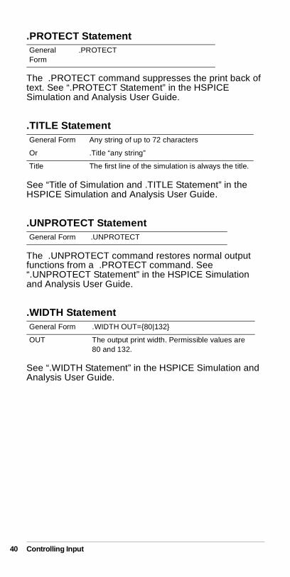
.PROTECT Statement
The .PROTECT command suppresses the print back of text. See “.PROTECT Statement” in the HSPICE Simulation and Analysis User Guide.
.TITLE Statement
See “Title of Simulation and .TITLE Statement” in the HSPICE Simulation and Analysis User Guide.
.UNPROTECT Statement
The .UNPROTECT command restores normal output functions from a .PROTECT command. See “.UNPROTECT Statement” in the HSPICE Simulation and Analysis User Guide.
.WIDTH Statement
See “.WIDTH Statement” in the HSPICE Simulation and Analysis User Guide.
General Form
.PROTECT
General Form Any string of up to 72 characters
Or .Title “any string”
Title The first line of the simulation is always the title.
General Form .UNPROTECT
General Form .WIDTH OUT={80|132}
OUT The output print width. Permissible values are 80 and 132.
Controlling Input
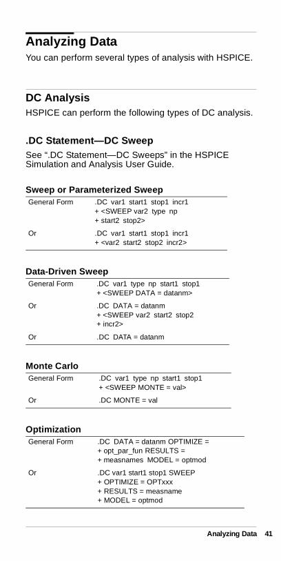
Analyzing DataYou can perform several types of analysis with HSPICE.
DC AnalysisHSPICE can perform the following types of DC analysis.
.DC Statement—DC SweepSee “.DC Statement—DC Sweeps” in the HSPICE Simulation and Analysis User Guide.
Sweep or Parameterized Sweep
Data-Driven Sweep
Monte Carlo
Optimization
General Form .DC var1 start1 stop1 incr1 + <SWEEP var2 type np+ start2 stop2>
Or .DC var1 start1 stop1 incr1+ <var2 start2 stop2 incr2>
General Form .DC var1 type np start1 stop1+ <SWEEP DATA = datanm>
Or .DC DATA = datanm + <SWEEP var2 start2 stop2+ incr2>
Or .DC DATA = datanm
General Form .DC var1 type np start1 stop1+ <SWEEP MONTE = val>
Or .DC MONTE = val
General Form .DC DATA = datanm OPTIMIZE =+ opt_par_fun RESULTS =+ measnames MODEL = optmod
Or .DC var1 start1 stop1 SWEEP + OPTIMIZE = OPTxxx + RESULTS = measname + MODEL = optmod
Analyzing Data 41
42
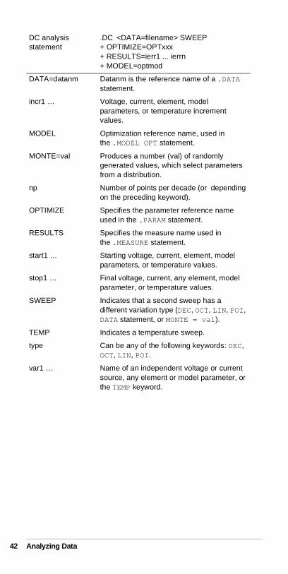
DC analysis statement
.DC <DATA=filename> SWEEP + OPTIMIZE=OPTxxx + RESULTS=ierr1 ... ierrn + MODEL=optmod
DATA=datanm Datanm is the reference name of a .DATA statement.
incr1 … Voltage, current, element, model parameters, or temperature increment values.
MODEL Optimization reference name, used in the .MODEL OPT statement.
MONTE=val Produces a number (val) of randomly generated values, which select parameters from a distribution.
np Number of points per decade (or depending on the preceding keyword).
OPTIMIZE Specifies the parameter reference name used in the .PARAM statement.
RESULTS Specifies the measure name used in the .MEASURE statement.
start1 … Starting voltage, current, element, model parameters, or temperature values.
stop1 … Final voltage, current, any element, model parameter, or temperature values.
SWEEP Indicates that a second sweep has a different variation type (DEC, OCT, LIN, POI, DATA statement, or MONTE = val).
TEMP Indicates a temperature sweep.
type Can be any of the following keywords: DEC, OCT, LIN, POI.
var1 … Name of an independent voltage or current source, any element or model parameter, or the TEMP keyword.
Analyzing Data
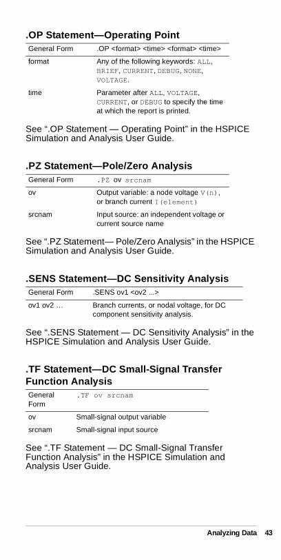
.OP Statement—Operating Point
See “.OP Statement — Operating Point” in the HSPICE Simulation and Analysis User Guide.
.PZ Statement—Pole/Zero Analysis
See “.PZ Statement— Pole/Zero Analysis” in the HSPICE Simulation and Analysis User Guide.
.SENS Statement—DC Sensitivity Analysis
See “.SENS Statement — DC Sensitivity Analysis” in the HSPICE Simulation and Analysis User Guide.
.TF Statement—DC Small-Signal Transfer Function Analysis
See “.TF Statement — DC Small-Signal Transfer Function Analysis” in the HSPICE Simulation and Analysis User Guide.
General Form .OP <format> <time> <format> <time>
format Any of the following keywords: ALL, BRIEF, CURRENT, DEBUG, NONE, VOLTAGE.
time Parameter after ALL, VOLTAGE, CURRENT, or DEBUG to specify the time at which the report is printed.
General Form .PZ ov srcnam
ov Output variable: a node voltage V(n), or branch current I(element)
srcnam Input source: an independent voltage or current source name
General Form .SENS ov1 <ov2 ...>
ov1 ov2 … Branch currents, or nodal voltage, for DC component sensitivity analysis.
General Form
.TF ov srcnam
ov Small-signal output variable
srcnam Small-signal input source
Analyzing Data 43
44
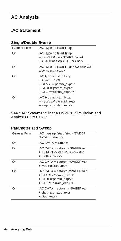
AC Analysis
.AC Statement
Single/Double Sweep
See “.AC Statement” in the HSPICE Simulation and Analysis User Guide.
Parameterized Sweep
General Form .AC type np fstart fstop
Or .AC type np fstart fstop + <SWEEP var <START=>start + <STOP=>stop <STEP=>incr>
Or .AC type np fstart fstop <SWEEP var type np start stop>
Or .AC type np fstart fstop + <SWEEP var + START="param_expr1"+ STOP="param_expr2" + STEP="param_expr3">
Or .AC type np fstart fstop + <SWEEP var start_expr + stop_expr step_expr>
General Form .AC type np fstart fstop <SWEEP DATA = datanm>
Or .AC DATA = datanm
Or .AC DATA = datanm <SWEEP var + <START=>start <STOP=>stop+ <STEP=>incr>
Or .AC DATA = datanm <SWEEP var + type np start stop>
Or .AC DATA = datanm <SWEEP var + START="param_expr1" + STOP="param_expr2" + STEP="param_expr3">
Or .AC DATA = datanm <SWEEP var + start_expr stop_expr + step_expr>
Analyzing Data
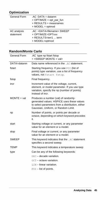
Optimization
Random/Monte Carlo
General Form .AC DATA = datanm + OPTIMIZE = opt_par_fun+ RESULTS = measnames + MODEL = optmod
AC analysis statement
.AC <DATA=filename> SWEEP + OPTIMIZE=OPTxxx + RESULTS=ierr1 ... ierrn + MODEL=optmod
General Form .AC type np fstart fstop + <SWEEP MONTE = val>
DATA=datanm Data name referenced in the .AC statement.
fstart Starting frequency. If you use POI (list of points) type variation, use a list of frequency values, not fstart fstop.
fstop Final frequency.
incr Increment value of the voltage, current, element, or model parameter. If you use type variation, specify the np (number of points) instead of incr.
MONTE = val Produces a number (val) of randomly-generated values. HSPICE uses these values to select parameters from a distribution, either Gaussian, Uniform, or Random Limit.
np Number of points, or points per decade or octave, depending on which keyword precedes it.
start Starting voltage or current, or any parameter value for an element or a model.
stop Final voltage or current, or any parameter value for an element or a model.
SWEEP This keyword indicates that the .AC statement specifies a second sweep.
TEMP This keyword indicates a temperature sweep
type Can be any of the following keywords:
DEC – decade variation.
OCT – octave variation.
LIN – linear variation.
POI – list of points.
Analyzing Data 45
46
.DISTO Statement—AC Small-Signal Distortion Analysis
See “.DISTO Statement — AC Small-Signal Distortion Analysis” in the HSPICE Simulation and Analysis User Guide.
.NOISE Statement—AC Noise Analysis
See “.NOISE Statement — AC Noise Analysis” in the HSPICE Simulation and Analysis User Guide.
.SAMPLE Statement—Noise Folding Analysis
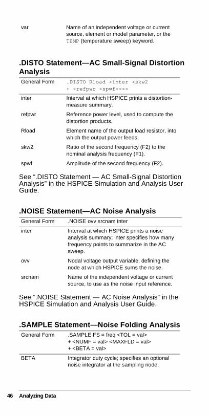
var Name of an independent voltage or current source, element or model parameter, or the TEMP (temperature sweep) keyword.
General Form .DISTO Rload <inter <skw2 + <refpwr <spwf>>>>
inter Interval at which HSPICE prints a distortion-measure summary.
refpwr Reference power level, used to compute the distortion products.
Rload Element name of the output load resistor, into which the output power feeds.
skw2 Ratio of the second frequency (F2) to the nominal analysis frequency (F1).
spwf Amplitude of the second frequency (F2).
General Form .NOISE ovv srcnam inter
inter Interval at which HSPICE prints a noise analysis summary; inter specifies how many frequency points to summarize in the AC sweep.
ovv Nodal voltage output variable, defining the node at which HSPICE sums the noise.
srcnam Name of the independent voltage or current source, to use as the noise input reference.
General Form .SAMPLE FS = freq <TOL = val>+ <NUMF = val> <MAXFLD = val>+ <BETA = val>
BETA Integrator duty cycle; specifies an optional noise integrator at the sampling node.
Analyzing Data
See “.SAMPLE Statement — Noise Folding Analysis” in the HSPICE Simulation and Analysis User Guide.
Small-Signal Network Analysis
.NET Statement—AC Network Analysis
One-port network
Two-port network
See “.NET Statement - AC Network Analysis” in the HSPICE Simulation and Analysis User Guide.
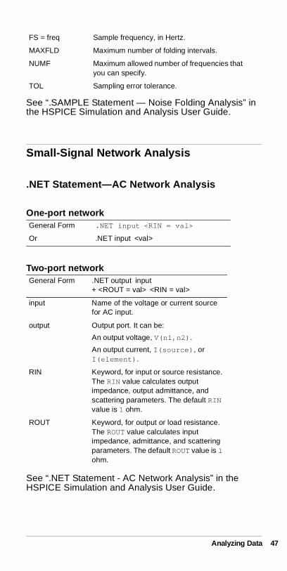
FS = freq Sample frequency, in Hertz.
MAXFLD Maximum number of folding intervals.
NUMF Maximum allowed number of frequencies that you can specify.
TOL Sampling error tolerance.
General Form .NET input <RIN = val>
Or .NET input <val>
General Form .NET output input+ <ROUT = val> <RIN = val>
input Name of the voltage or current source for AC input.
output Output port. It can be:
An output voltage, V(n1,n2).
An output current, I(source), or I(element).
RIN Keyword, for input or source resistance. The RIN value calculates output impedance, output admittance, and scattering parameters. The default RIN value is 1 ohm.
ROUT Keyword, for output or load resistance. The ROUT value calculates input impedance, admittance, and scattering parameters. The default ROUT value is 1 ohm.
Analyzing Data 47
48
AC Network Analysis—Output Specification
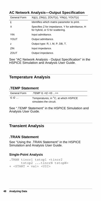
See “AC Network Analysis - Output Specification” in the HSPICE Simulation and Analysis User Guide.
Temperature Analysis
.TEMP Statement
See “.TEMP Statement” in the HSPICE Simulation and Analysis User Guide.
Transient Analysis
.TRAN StatementSee “Using the .TRAN Statement” in the HSPICE Simulation and Analysis User Guide.
Single-Point Analysis
.TRAN tincr1 tstop1 <tincr2tstop2 ...tincrN tstopN>
+ <START = val> <UIC>
General Form Xij(z), ZIN(z), ZOUT(z), YIN(z), YOUT(z)
ij Identifies which matrix parameter to print.
X Specifies Z for impedance, Y for admittance, H for hybrid, or S for scattering.
YIN Input admittance.
YOUT Output admittance.
z Output type: R, I, M, P, DB, T.
ZIN Input impedance.
ZOUT Output impedance.
General Form .TEMP t1 <t2 <t3 ...>>
t1 t2 … Temperatures, in °C, at which HSPICE simulates the circuit.
Analyzing Data
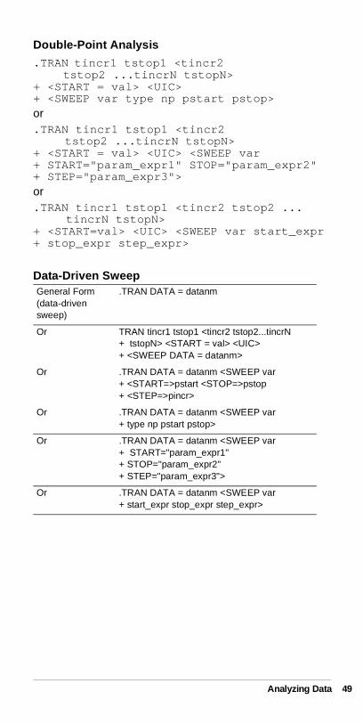
Double-Point Analysis
.TRAN tincr1 tstop1 <tincr2tstop2 ...tincrN tstopN>
+ <START = val> <UIC>+ <SWEEP var type np pstart pstop>or.TRAN tincr1 tstop1 <tincr2
tstop2 ...tincrN tstopN> + <START = val> <UIC> <SWEEP var + START="param_expr1" STOP="param_expr2"+ STEP="param_expr3">or.TRAN tincr1 tstop1 <tincr2 tstop2 ...
tincrN tstopN> + <START=val> <UIC> <SWEEP var start_expr + stop_expr step_expr>
Data-Driven SweepGeneral Form(data-driven sweep)
.TRAN DATA = datanm
Or TRAN tincr1 tstop1 <tincr2 tstop2...tincrN+ tstopN> <START = val> <UIC>+ <SWEEP DATA = datanm>
Or .TRAN DATA = datanm <SWEEP var+ <START=>pstart <STOP=>pstop + <STEP=>pincr>
Or .TRAN DATA = datanm <SWEEP var+ type np pstart pstop>
Or .TRAN DATA = datanm <SWEEP var+ START="param_expr1" + STOP="param_expr2" + STEP="param_expr3">
Or .TRAN DATA = datanm <SWEEP var + start_expr stop_expr step_expr>
Analyzing Data 49
50
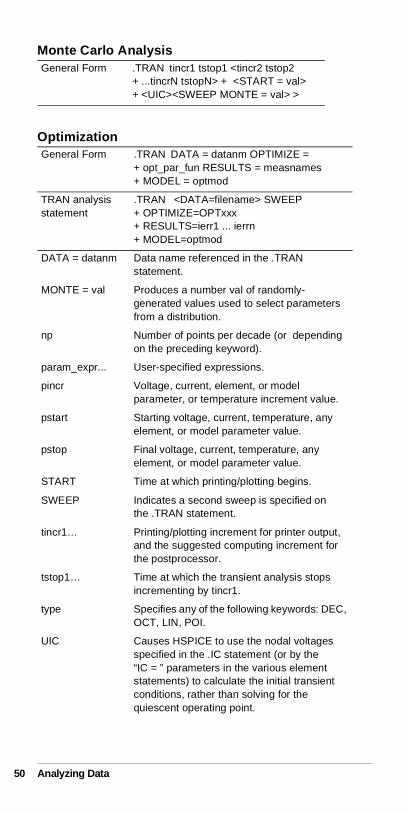
Monte Carlo Analysis
Optimization
General Form .TRAN tincr1 tstop1 <tincr2 tstop2+ ...tincrN tstopN> + <START = val>+ <UIC><SWEEP MONTE = val> >
General Form .TRAN DATA = datanm OPTIMIZE =+ opt_par_fun RESULTS = measnames+ MODEL = optmod
TRAN analysis statement
.TRAN <DATA=filename> SWEEP + OPTIMIZE=OPTxxx+ RESULTS=ierr1 ... ierrn + MODEL=optmod
DATA = datanm Data name referenced in the .TRAN statement.
MONTE = val Produces a number val of randomly-generated values used to select parameters from a distribution.
np Number of points per decade (or depending on the preceding keyword).
param_expr... User-specified expressions.
pincr Voltage, current, element, or model parameter, or temperature increment value.
pstart Starting voltage, current, temperature, any element, or model parameter value.
pstop Final voltage, current, temperature, any element, or model parameter value.
START Time at which printing/plotting begins.
SWEEP Indicates a second sweep is specified on the .TRAN statement.
tincr1… Printing/plotting increment for printer output, and the suggested computing increment for the postprocessor.
tstop1… Time at which the transient analysis stops incrementing by tincr1.
type Specifies any of the following keywords: DEC, OCT, LIN, POI.
UIC Causes HSPICE to use the nodal voltages specified in the .IC statement (or by the “IC = ” parameters in the various element statements) to calculate the initial transient conditions, rather than solving for the quiescent operating point.
Analyzing Data
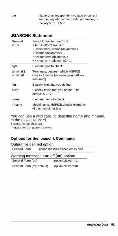
.BIASCHK Statement
You can use a wild card, to describe name and mname, in the biaschk card.? stands for one character. * stands for 0 or more characters.
Options for the .biaschk Command
Output file defined option:
Warning message turn off (on) option:
var Name of an independent voltage or current source, any element or model parameter, or the keyword TEMP.
General Form
.biaschk type terminal1=t1 + terminal2=t2 limit=lim+ <noise=ns><name=devname1>+ <name=devname2>... + <mname=modelname1>+ <mname=modelname2> ...
type Element type to check.
terminal 1, terminal2
Terminals, between which HSPICE checks (checks between terminal1 and terminal2)
limit Biaschk limit that you define.
noise Biaschk noise that you define. The default is 0.1v.
name Element name to check.
mname Model name. HSPICE checks elements of this model, for bias.
General Form .option biasfile=biaschk/mos.bias
General Form (on) .option biawarn=1
General Form (off, default) .option biawarn=0
Analyzing Data 51
52
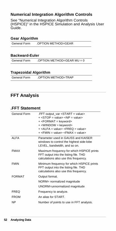
Numerical Integration Algorithm ControlsSee “Numerical Integration Algorithm Controls (HSPICE)” in the HSPICE Simulation and Analysis User Guide.
Gear Algorithm
Backward-Euler
Trapezoidal Algorithm
FFT Analysis
.FFT Statement
General Form .OPTION METHOD=GEAR
General Form .OPTION METHOD=GEAR MU = 0
General Form .OPTION METHOD=TRAP
General Form .FFT output_var <START = value>+ <STOP = value> <NP = value>+ <FORMAT = keyword>+ <WINDOW = keyword> + <ALFA = value> <FREQ = value>+ <FMIN = value> <FMAX = value>
ALFA Parameter used in GAUSS and KAISER windows to control the highest side-lobe LEVEL, bandwidth, and so on.
FMAX Maximum frequency for which HSPICE prints FFT output into the listing file. THD calculations also use this frequency.
FMIN Minimum frequency for which HSPICE prints FFT output into the listing file. THD calculations also use this frequency.
FORMAT Output format.
NORM= normalized magnitude
UNORM=unnormalized magnitude
FREQ Frequency to analyze.
FROM An alias for START.
NP Number of points to use in FFT analysis.
Analyzing Data
See “.FFT Statement” in the HSPICE Applications Manual.
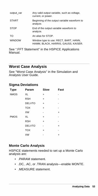
Worst Case AnalysisSee “Worst Case Analysis” in the Simulation and Analysis User Guide.
Sigma Deviations
Monte Carlo Analysis HSPICE statements needed to set up a Monte Carlo analysis are:
• .PARAM statement.
• .DC, .AC, or .TRAN analysis—enable MONTE.
• .MEASURE statement.
output_var Any valid output variable, such as voltage, current, or power.
START Beginning of the output variable waveform to analyze.
STOP End of the output variable waveform to analyze.
TO An alias for STOP.
WINDOW Window type to use: RECT, BART, HANN, HAMM, BLACK, HARRIS, GAUSS, KAISER.
Type Param Slow Fast
NMOS XL + -
RSH + -
DELVTO + -
TOX + -
XW - +
PMOS XL + -
RSH + -
DELVTO - +
TOX + -
XW - +
Analyzing Data 53
54
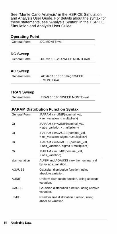
See “Monte Carlo Analysis” in the HSPICE Simulation and Analysis User Guide. For details about the syntax for these statements, see “Analysis Syntax” in the HSPICE Simulation and Analysis User Guide.
Operating Point
DC Sweep
AC Sweep
TRAN Sweep
.PARAM Distribution Function Syntax
General Form .DC MONTE=val
General Form .DC vin 1 5 .25 SWEEP MONTE=val
General Form .AC dec 10 100 10meg SWEEP+ MONTE=val
General Form .TRAN 1n 10n SWEEP MONTE=val
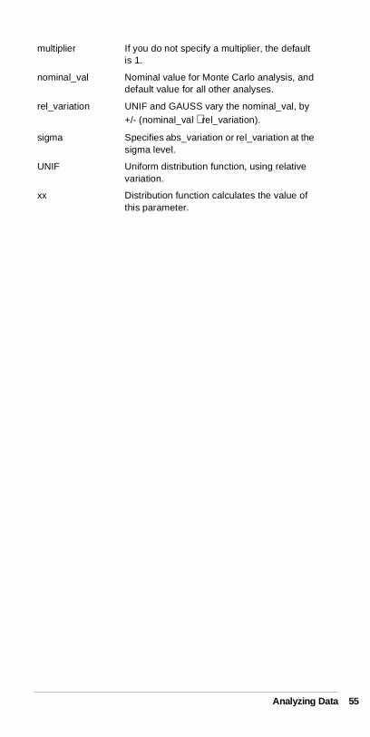
General Form .PARAM xx=UNIF(nominal_val,+ rel_variation <, multiplier>)
Or .PARAM xx=AUNIF(nominal_val,+ abs_variation <,multiplier>)
Or .PARAM xx=GAUSS(nominal_val,+ rel_variation, sigma <,multiplier>)
Or .PARAM xx=AGAUSS(nominal_val,+ abs_variation, sigma <,multiplier>)
Or .PARAM xx=LIMIT(nominal_val,+ abs_variation)
abs_variation AUNIF and AGAUSS vary the nominal_val by +/- abs_variation.
AGAUSS Gaussian distribution function, using absolute variation.
AUNIF Uniform distribution function, using absolute variation.
GAUSS Gaussian distribution function, using relative variation.
LIMIT Random limit distribution function, using absolute variation.
Analyzing Data
1-
multiplier If you do not specify a multiplier, the default is 1.
nominal_val Nominal value for Monte Carlo analysis, and default value for all other analyses.
rel_variation UNIF and GAUSS vary the nominal_val, by +/- (nominal_val ⋅ rel_variation).
sigma Specifies abs_variation or rel_variation at the sigma level.
UNIF Uniform distribution function, using relative variation.
xx Distribution function calculates the value of this parameter.
Analyzing Data 55
56
Optimizing DataThis chapter briefly describes how to optimize your design data.
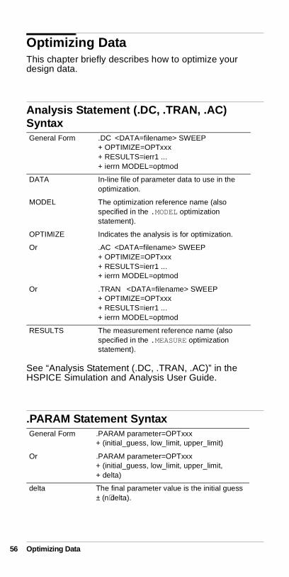
Analysis Statement (.DC, .TRAN, .AC) Syntax
See “Analysis Statement (.DC, .TRAN, .AC)” in the HSPICE Simulation and Analysis User Guide.
.PARAM Statement Syntax
General Form .DC <DATA=filename> SWEEP+ OPTIMIZE=OPTxxx + RESULTS=ierr1 ...+ ierrn MODEL=optmod
DATA In-line file of parameter data to use in the optimization.
MODEL The optimization reference name (also specified in the .MODEL optimization statement).
OPTIMIZE Indicates the analysis is for optimization.
Or .AC <DATA=filename> SWEEP+ OPTIMIZE=OPTxxx + RESULTS=ierr1 ...+ ierrn MODEL=optmod
Or .TRAN <DATA=filename> SWEEP+ OPTIMIZE=OPTxxx + RESULTS=ierr1 ... + ierrn MODEL=optmod
RESULTS The measurement reference name (also specified in the .MEASURE optimization statement).
General Form .PARAM parameter=OPTxxx+ (initial_guess, low_limit, upper_limit)
Or .PARAM parameter=OPTxxx+ (initial_guess, low_limit, upper_limit,+ delta)
delta The final parameter value is the initial guess ± (n⋅delta).
Optimizing Data
See “.PARAM Statement” in the HSPICE Simulation and Analysis User Guide.
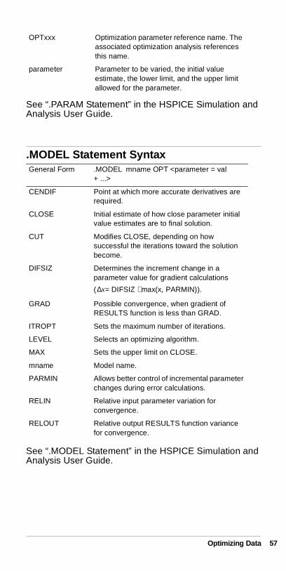
.MODEL Statement Syntax
See “.MODEL Statement” in the HSPICE Simulation and Analysis User Guide.
OPTxxx Optimization parameter reference name. The associated optimization analysis references this name.
parameter Parameter to be varied, the initial value estimate, the lower limit, and the upper limit allowed for the parameter.
General Form .MODEL mname OPT <parameter = val+ ...>
CENDIF Point at which more accurate derivatives are required.
CLOSE Initial estimate of how close parameter initial value estimates are to final solution.
CUT Modifies CLOSE, depending on how successful the iterations toward the solution become.
DIFSIZ Determines the increment change in a parameter value for gradient calculations
( = DIFSIZ ⋅ max(x, PARMIN)).
GRAD Possible convergence, when gradient of RESULTS function is less than GRAD.
ITROPT Sets the maximum number of iterations.
LEVEL Selects an optimizing algorithm.
MAX Sets the upper limit on CLOSE.
mname Model name.
PARMIN Allows better control of incremental parameter changes during error calculations.
RELIN Relative input parameter variation for convergence.
RELOUT Relative output RESULTS function variance for convergence.
∆x
Optimizing Data 57
58
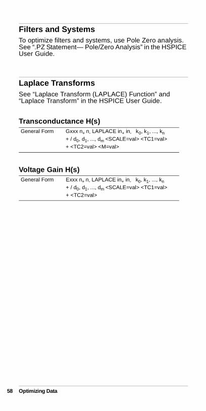
Filters and SystemsTo optimize filters and systems, use Pole Zero analysis. See “.PZ Statement— Pole/Zero Analysis” in the HSPICE User Guide.
Laplace TransformsSee “Laplace Transform (LAPLACE) Function” and “Laplace Transform” in the HSPICE User Guide.
Transconductance H(s)
Voltage Gain H(s)
2-
General Form Gxxx n+ n- LAPLACE in+ in- k0, k1, ..., kn
+ / d0, d1, ..., dm <SCALE=val> <TC1=val>
+ <TC2=val> <M=val>
General Form Exxx n+ n- LAPLACE in+ in- k0, k1, ..., kn
+ / d0, d1, ..., dm <SCALE=val> <TC1=val>
+ <TC2=val>
Optimizing Data
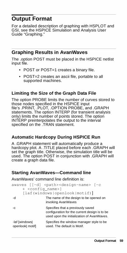
Output FormatFor a detailed description of graphing with HSPLOT and GSI, see the HSPICE Simulation and Analysis User Guide “Graphing.”
Graphing Results in AvanWavesThe .option POST must be placed in the HSPICE netlist input file.
• POST or POST=1 creates a binary file.
• POST=2 creates an ascii file, portable to all supported machines.
Limiting the Size of the Graph Data FileThe option PROBE limits the number of curves stored to those nodes specified in the HSPICE input file’s .PRINT, .PLOT, .OPTION PROBE, and .GRAPH statements. The option INTERP (for transient analysis only) limits the number of points stored. The option INTERP preinterpolates the output to the interval specified on the .TRAN statement.
Automatic Hardcopy During HSPICE RunA .GRAPH statement will automatically produce a hardcopy plot. A .TITLE placed before each .GRAPH will set the graph title. Otherwise, the simulation title will be used. The option POST in conjunction with .GRAPH will create a graph data file.
Starting AvanWaves—Command lineAvanWaves’ command line definition is:awaves [[-d] <path><design-name> [-c
+ <config_name>][laf(windows|openlook|motif)]
-d The name of the design to be opened on invoking AvanWaves
-c Specifies that a previously saved configuration for the current design is to be used upon the initialization of AvanWaves.
-laf [windows| openlook| motif]
Specifies the window manager style to be used. The default is Motif.
Output Format 59
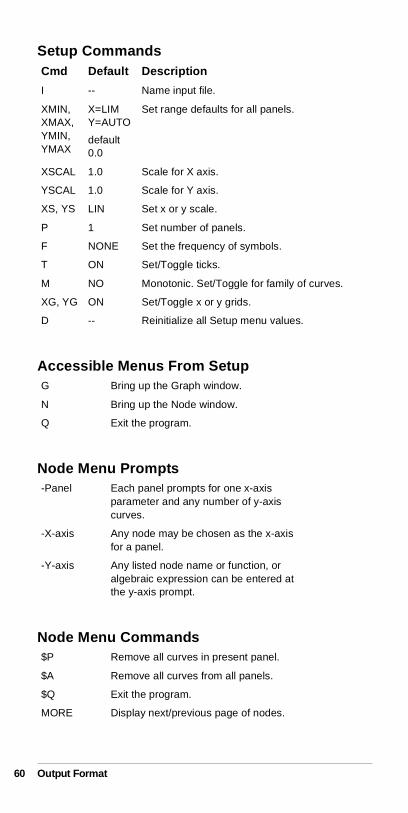
60
Setup Commands
Accessible Menus From Setup
Node Menu Prompts
Node Menu Commands
Cmd Default Description
I -- Name input file.
XMIN, XMAX, YMIN, YMAX
X=LIMY=AUTO
default 0.0
Set range defaults for all panels.
XSCAL 1.0 Scale for X axis.
YSCAL 1.0 Scale for Y axis.
XS, YS LIN Set x or y scale.
P 1 Set number of panels.
F NONE Set the frequency of symbols.
T ON Set/Toggle ticks.
M NO Monotonic. Set/Toggle for family of curves.
XG, YG ON Set/Toggle x or y grids.
D -- Reinitialize all Setup menu values.
G Bring up the Graph window.
N Bring up the Node window.
Q Exit the program.
-Panel Each panel prompts for one x-axis parameter and any number of y-axis curves.
-X-axis Any node may be chosen as the x-axis for a panel.
-Y-axis Any listed node name or function, or algebraic expression can be entered at the y-axis prompt.
$P Remove all curves in present panel.
$A Remove all curves from all panels.
$Q Exit the program.
MORE Display next/previous page of nodes.
Output Format
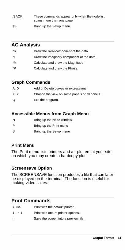
AC Analysis
Graph Commands
Accessible Menus from Graph Menu
Print MenuThe Print menu lists printers and /or plotters at your site on which you may create a hardcopy plot.
Screensave OptionThe SCREENSAVE function produces a file that can later be displayed on the terminal. The function is useful for making video slides.
Print Commands
/BACK These commands appear only when the node list spans more than one page.
$S Bring up the Setup menu.
*R Draw the Real component of the data.
*I Draw the Imaginary component of the data.
*M Calculate and draw the Magnitude.
*P Calculate and draw the Phase.
A, D Add or Delete curves or expressions.
X, Y Change the view on some panels or all panels.
Q Exit the program.
N Bring up the Node window
P Bring up the Print menu
S Bring up the Setup menu
<CR> Print with the default printer.
1…n-1 Print with one of printer options.
n Save the screen into a preview file.
Output Format 61
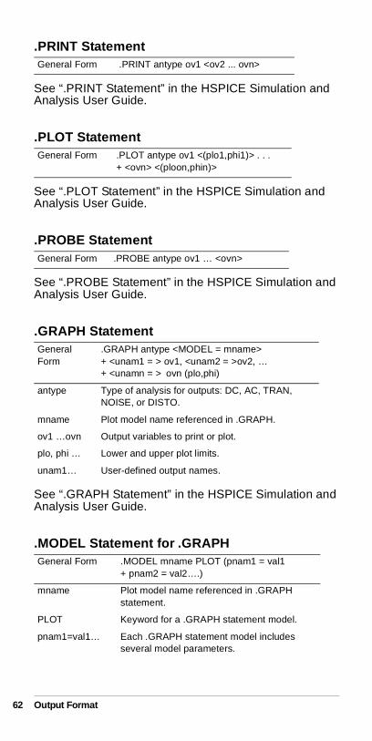
62
.PRINT Statement
See “.PRINT Statement” in the HSPICE Simulation and Analysis User Guide.
.PLOT Statement
See “.PLOT Statement” in the HSPICE Simulation and Analysis User Guide.
.PROBE Statement
See “.PROBE Statement” in the HSPICE Simulation and Analysis User Guide.
.GRAPH Statement
See “.GRAPH Statement” in the HSPICE Simulation and Analysis User Guide.
.MODEL Statement for .GRAPH
General Form .PRINT antype ov1 <ov2 ... ovn>
General Form .PLOT antype ov1 <(plo1,phi1)> . . .+ <ovn> <(ploon,phin)>
General Form .PROBE antype ov1 … <ovn>
General Form
.GRAPH antype <MODEL = mname>+ <unam1 = > ov1, <unam2 = >ov2, …+ <unamn = > ovn (plo,phi)
antype Type of analysis for outputs: DC, AC, TRAN, NOISE, or DISTO.
mname Plot model name referenced in .GRAPH.
ov1 …ovn Output variables to print or plot.
plo, phi … Lower and upper plot limits.
unam1… User-defined output names.
General Form .MODEL mname PLOT (pnam1 = val1+ pnam2 = val2….)
mname Plot model name referenced in .GRAPH statement.
PLOT Keyword for a .GRAPH statement model.
pnam1=val1… Each .GRAPH statement model includes several model parameters.
Output Format
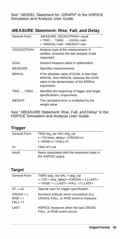
See “.MODEL Statement for .GRAPH” in the HSPICE Simulation and Analysis User Guide.
.MEASURE Statement: Rise, Fall, and Delay
See “.MEASURE Statement: Rise, Fall, and Delay” in the HSPICE Simulation and Analysis User Guide.
Trigger
Target
General Form .MEASURE <DC|AC|TRAN> result+ TRIG … TARG … <GOAL=val>+ <MINVAL=val> <WEIGHT=val>
<DC|AC|TRAN> Analysis type of the measurement. If omitted, assumes the last analysis mode requested.
GOAL Desired measure value in optimization.
MEASURE Specifies measurements.
MINVAL If the absolute value of GOAL is less than MINVAL, then MINVAL replaces the GOAL value in the denominator of the ERRfun expression.
TRIG…, TARG … Identifies the beginning of trigger and target specifications, respectively.
WEIGHT The calculated error is multiplied by the weight value.
General Form TRIG trig_var VAL=trig_val+ <TD=time_delay> <CROSS=c>+ <RISE=r> <FALL=f>
Or TRIG AT=val
result Name associated with the measured value in the HSPICE output.
General Form TARG targ_var VAL = targ_val+ <TD = time_delay> <CROSS = c | LAST>+ <RISE = r | LAST> <FALL = f | LAST>
AT = val Special case for trigger specification.
CROSS = cRISE = rFALL = f
Numbers indicate which occurrence of a CROSS, FALL, or RISE event to measure.
LAST HSPICE measures when the last CROSS, FALL, or RISE event occurs.
Output Format 63
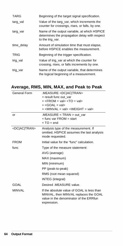
64
Average, RMS, MIN, MAX, and Peak to Peak
TARG Beginning of the target signal specification.
targ_val Value of the targ_var, which increments the counter for crossings, rises, or falls, by one.
targ_var Name of the output variable, at which HSPICE determines the propagation delay with respect to the trig_var.
time_delay Amount of simulation time that must elapse, before HSPICE enables the measurement.
TRIG Beginning of the trigger specification.
trig_val Value of trig_var at which the counter for crossing, rises, or falls increments by one.
trig_var Name of the output variable, that determines the logical beginning of a measurement.
General Form .MEASURE <DC|AC|TRAN>+ result func out_var + <FROM = val> <TO = val> + <GOAL = val>+ <MINVAL = val> <WEIGHT = val>
or .MEASURE < TRAN > out_var+ func var FROM = start + TO = end
<DC|AC|TRAN> Analysis type of the measurement. If omitted, HSPICE assumes the last analysis mode requested.
FROM Initial value for the “func” calculation.
func Type of the measure statement:
AVG (average)
MAX (maximum)
MIN (minimum)
PP (peak-to-peak)
RMS (root mean squared)
INTEG (integral)
GOAL Desired .MEASURE value.
MINVAL If the absolute value of GOAL is less than MINVAL, then MINVAL replaces the GOAL value in the denominator of the ERRfun expression.
Output Format
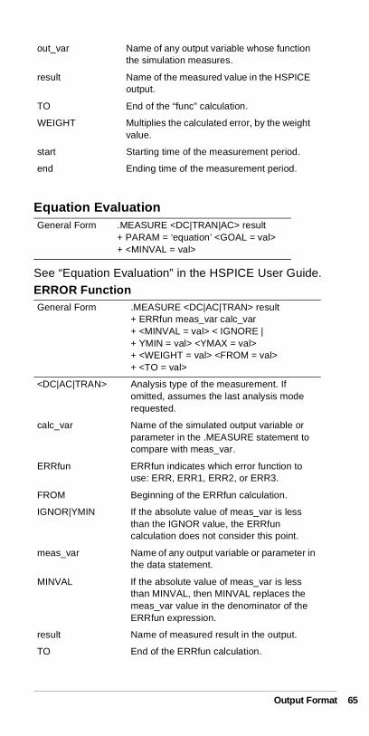
Equation Evaluation
See “Equation Evaluation” in the HSPICE User Guide.ERROR Function
out_var Name of any output variable whose function the simulation measures.
result Name of the measured value in the HSPICE output.
TO End of the “func” calculation.
WEIGHT Multiplies the calculated error, by the weight value.
start Starting time of the measurement period.
end Ending time of the measurement period.
General Form .MEASURE <DC|TRAN|AC> result+ PARAM = ‘equation’ <GOAL = val>+ <MINVAL = val>
General Form .MEASURE <DC|AC|TRAN> result+ ERRfun meas_var calc_var+ <MINVAL = val> < IGNORE |+ YMIN = val> <YMAX = val>+ <WEIGHT = val> <FROM = val>+ <TO = val>
<DC|AC|TRAN> Analysis type of the measurement. If omitted, assumes the last analysis mode requested.
calc_var Name of the simulated output variable or parameter in the .MEASURE statement to compare with meas_var.
ERRfun ERRfun indicates which error function to use: ERR, ERR1, ERR2, or ERR3.
FROM Beginning of the ERRfun calculation.
IGNOR|YMIN If the absolute value of meas_var is less than the IGNOR value, the ERRfun calculation does not consider this point.
meas_var Name of any output variable or parameter in the data statement.
MINVAL If the absolute value of meas_var is less than MINVAL, then MINVAL replaces the meas_var value in the denominator of the ERRfun expression.
result Name of measured result in the output.
TO End of the ERRfun calculation.
Output Format 65
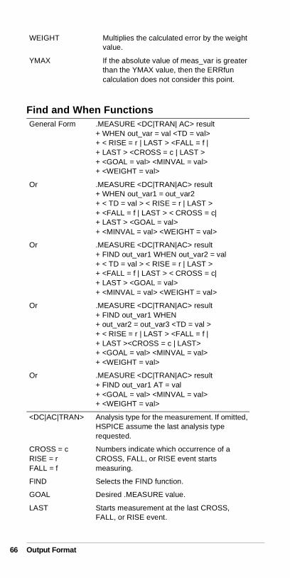
66
Find and When Functions
WEIGHT Multiplies the calculated error by the weight value.
YMAX If the absolute value of meas_var is greater than the YMAX value, then the ERRfun calculation does not consider this point.
General Form .MEASURE <DC|TRAN| AC> result+ WHEN out_var = val <TD = val>+ < RISE = r | LAST > <FALL = f |+ LAST > <CROSS = c | LAST >+ <GOAL = val> <MINVAL = val>+ <WEIGHT = val>
Or .MEASURE <DC|TRAN|AC> result+ WHEN out_var1 = out_var2+ < TD = val > < RISE = r | LAST >+ <FALL = f | LAST > < CROSS = c|+ LAST > <GOAL = val>+ <MINVAL = val> <WEIGHT = val>
Or .MEASURE <DC|TRAN|AC> result+ FIND out_var1 WHEN out_var2 = val+ < TD = val > < RISE = r | LAST >+ <FALL = f | LAST > < CROSS = c|+ LAST > <GOAL = val>+ <MINVAL = val> <WEIGHT = val>
Or .MEASURE <DC|TRAN|AC> result+ FIND out_var1 WHEN+ out_var2 = out_var3 <TD = val >+ < RISE = r | LAST > <FALL = f |+ LAST ><CROSS = c | LAST>+ <GOAL = val> <MINVAL = val>+ <WEIGHT = val>
Or .MEASURE <DC|TRAN|AC> result+ FIND out_var1 AT = val+ <GOAL = val> <MINVAL = val>+ <WEIGHT = val>
<DC|AC|TRAN> Analysis type for the measurement. If omitted, HSPICE assume the last analysis type requested.
CROSS = cRISE = rFALL = f
Numbers indicate which occurrence of a CROSS, FALL, or RISE event starts measuring.
FIND Selects the FIND function.
GOAL Desired .MEASURE value.
LAST Starts measurement at the last CROSS, FALL, or RISE event.
Output Format
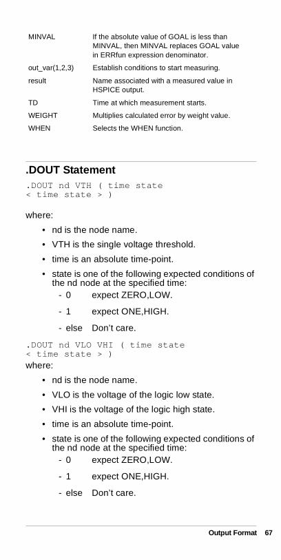
.DOUT Statement
.DOUT nd VTH ( time state < time state > )
where:
• nd is the node name.
• VTH is the single voltage threshold.
• time is an absolute time-point.
• state is one of the following expected conditions of the nd node at the specified time:
- 0 expect ZERO,LOW.
- 1 expect ONE,HIGH.
- else Don’t care.
.DOUT nd VLO VHI ( time state < time state > )where:
• nd is the node name.
• VLO is the voltage of the logic low state.
• VHI is the voltage of the logic high state.
• time is an absolute time-point.
• state is one of the following expected conditions of the nd node at the specified time:
- 0 expect ZERO,LOW.
- 1 expect ONE,HIGH.
- else Don’t care.
MINVAL If the absolute value of GOAL is less than MINVAL, then MINVAL replaces GOAL value in ERRfun expression denominator.
out_var(1,2,3) Establish conditions to start measuring.
result Name associated with a measured value in HSPICE output.
TD Time at which measurement starts.
WEIGHT Multiplies calculated error by weight value.
WHEN Selects the WHEN function.
Output Format 67
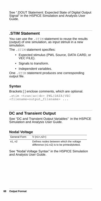
68
See “.DOUT Statement: Expected State of Digital Output Signal” in the HSPICE Simulation and Analysis User Guide.
.STIM StatementYou can use the .STIM statement to reuse the results (output) of one simulation, as input stimuli in a new simulation.The .STIM statement specifies:
• Expected stimulus (PWL Source, DATA CARD, or VEC FILE).
• Signals to transform.
• Independent variables.One .STIM statement produces one corresponding output file.
SyntaxBrackets [ ] enclose comments, which are optional..stim <tran|ac|dc> PWL|DATA|VEC <filename=output_filename> ...
DC and Transient OutputSee “DC and Transient Output Variables” in the HSPICE Simulation and Analysis User Guide.
Nodal Voltage
See “Nodal Voltage Syntax” in the HSPICE Simulation and Analysis User Guide.
General Form V (n1<,n2>)
n1, n2 Defines nodes between which the voltage difference (n1-n2) is to be printed/plotted.
Output Format
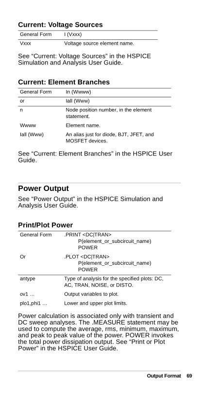
Current: Voltage Sources
See “Current: Voltage Sources” in the HSPICE Simulation and Analysis User Guide.
Current: Element Branches
See “Current: Element Branches” in the HSPICE User Guide.
Power OutputSee “Power Output” in the HSPICE Simulation and Analysis User Guide.
Print/Plot Power
Power calculation is associated only with transient and DC sweep analyses. The .MEASURE statement may be used to compute the average, rms, minimum, maximum, and peak to peak value of the power. POWER invokes the total power dissipation output. See “Print or Plot Power” in the HSPICE User Guide.
General Form I (Vxxx)
Vxxx Voltage source element name.
General Form In (Wwww)
or Iall (Www)
n Node position number, in the element statement.
Wwww Element name.
Iall (Www) An alias just for diode, BJT, JFET, and MOSFET devices.
General Form .PRINT <DC|TRAN>P(element_or_subcircuit_name)POWER
Or .PLOT <DC|TRAN>P(element_or_subcircuit_name)POWER
antype Type of analysis for the specified plots: DC, AC, TRAN, NOISE, or DISTO.
ov1 … Output variables to plot.
plo1,phi1 … Lower and upper plot limits.
Output Format 69
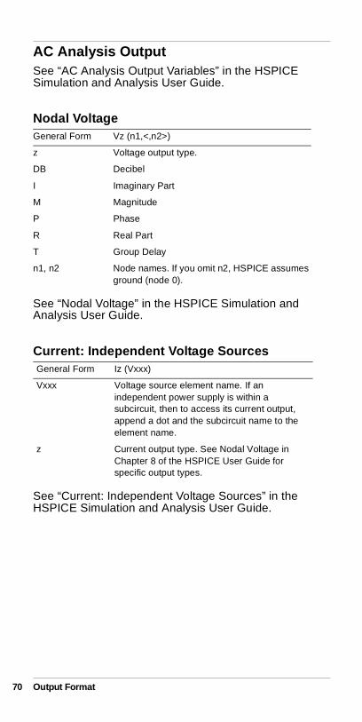
70
AC Analysis OutputSee “AC Analysis Output Variables” in the HSPICE Simulation and Analysis User Guide.
Nodal Voltage
See “Nodal Voltage” in the HSPICE Simulation and Analysis User Guide.
Current: Independent Voltage Sources
See “Current: Independent Voltage Sources” in the HSPICE Simulation and Analysis User Guide.
General Form Vz (n1,<,n2>)
z Voltage output type.
DB Decibel
I Imaginary Part
M Magnitude
P Phase
R Real Part
T Group Delay
n1, n2 Node names. If you omit n2, HSPICE assumes ground (node 0).
General Form Iz (Vxxx)
Vxxx Voltage source element name. If an independent power supply is within a subcircuit, then to access its current output, append a dot and the subcircuit name to the element name.
z Current output type. See Nodal Voltage in Chapter 8 of the HSPICE User Guide for specific output types.
Output Format
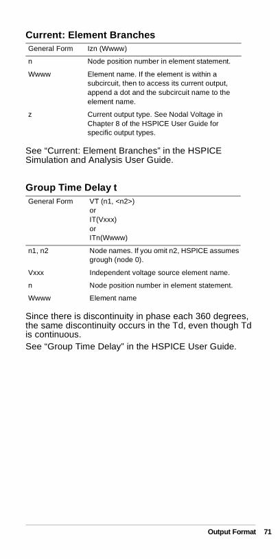
Current: Element Branches
See “Current: Element Branches” in the HSPICE Simulation and Analysis User Guide.
Group Time Delay t
Since there is discontinuity in phase each 360 degrees, the same discontinuity occurs in the Td, even though Td is continuous.See “Group Time Delay” in the HSPICE User Guide.
General Form Izn (Wwww)
n Node position number in element statement.
Wwww Element name. If the element is within a subcircuit, then to access its current output, append a dot and the subcircuit name to the element name.
z Current output type. See Nodal Voltage in Chapter 8 of the HSPICE User Guide for specific output types.
General Form VT (n1, <n2>)orIT(Vxxx)orITn(Wwww)
n1, n2 Node names. If you omit n2, HSPICE assumes grough (node 0).
Vxxx Independent voltage source element name.
n Node position number in element statement.
Wwww Element name
Output Format 71
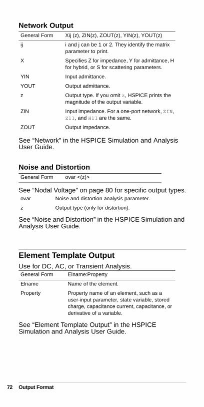
72
Network Output
See “Network” in the HSPICE Simulation and Analysis User Guide.
Noise and Distortion
See “Nodal Voltage” on page 80 for specific output types.
See “Noise and Distortion” in the HSPICE Simulation and Analysis User Guide.
Element Template OutputUse for DC, AC, or Transient Analysis.
See “Element Template Output” in the HSPICE Simulation and Analysis User Guide.
General Form Xij (z), ZIN(z), ZOUT(z), YIN(z), YOUT(z)
ij i and j can be 1 or 2. They identify the matrix parameter to print.
X Specifies Z for impedance, Y for admittance, H for hybrid, or S for scattering parameters.
YIN Input admittance.
YOUT Output admittance.
z Output type. If you omit z, HSPICE prints the magnitude of the output variable.
ZIN Input impedance. For a one-port network, ZIN, Z11, and H11 are the same.
ZOUT Output impedance.
General Form ovar <(z)>
ovar Noise and distortion analysis parameter.
z Output type (only for distortion).
General Form Elname:Property
Elname Name of the element.
Property Property name of an element, such as a user-input parameter, state variable, stored charge, capacitance current, capacitance, or derivative of a variable.
Output Format
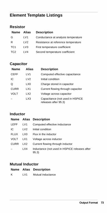
Element Template Listings
Resistor
Capacitor
Inductor
Mutual Inductor
Name Alias Description
G LV1 Conductance at analysis temperature
R LV2 Resistance at reference temperature
TC1 LV3 First temperature coefficient
TC2 LV4 Second temperature coefficient
Name Alias Description
CEFF LV1 Computed effective capacitance
IC LV2 Initial condition
Q LX0 Charge stored in capacitor
CURR LX1 Current flowing through capacitor
VOLT LX2 Voltage across capacitor
– LX3 Capacitance (not used in HSPICE releases after 95.3)
Name Alias Description
LEFF LV1 Computed effective inductance
IC LV2 Initial condition
FLUX LX0 Flux in the inductor
VOLT LX1 Voltage across inductor
CURR LX2 Current flowing through inductor
– LX4 Inductance (not used in HSPICE releases after 95.3)
Name Alias Description
K LV1 Mutual inductance
Output Format 73
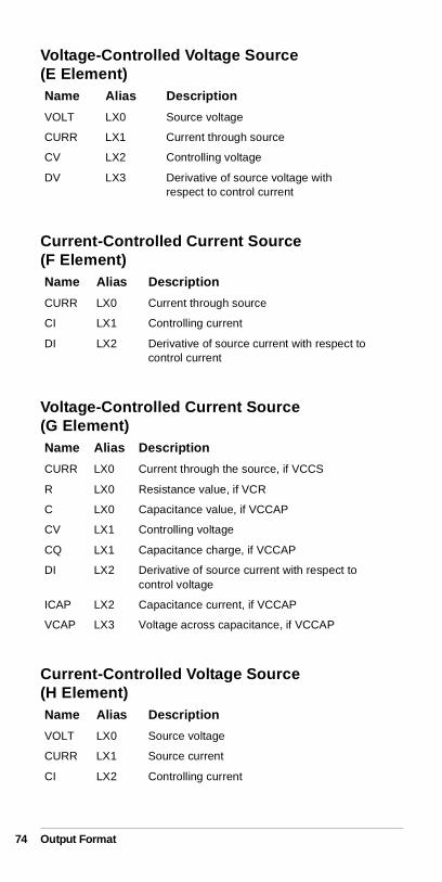
74
Voltage-Controlled Voltage Source (E Element)
Current-Controlled Current Source (F Element)
Voltage-Controlled Current Source (G Element)
Current-Controlled Voltage Source (H Element)
Name Alias Description
VOLT LX0 Source voltage
CURR LX1 Current through source
CV LX2 Controlling voltage
DV LX3 Derivative of source voltage with respect to control current
Name Alias Description
CURR LX0 Current through source
CI LX1 Controlling current
DI LX2 Derivative of source current with respect to control current
Name Alias Description
CURR LX0 Current through the source, if VCCS
R LX0 Resistance value, if VCR
C LX0 Capacitance value, if VCCAP
CV LX1 Controlling voltage
CQ LX1 Capacitance charge, if VCCAP
DI LX2 Derivative of source current with respect to control voltage
ICAP LX2 Capacitance current, if VCCAP
VCAP LX3 Voltage across capacitance, if VCCAP
Name Alias Description
VOLT LX0 Source voltage
CURR LX1 Source current
CI LX2 Controlling current
Output Format
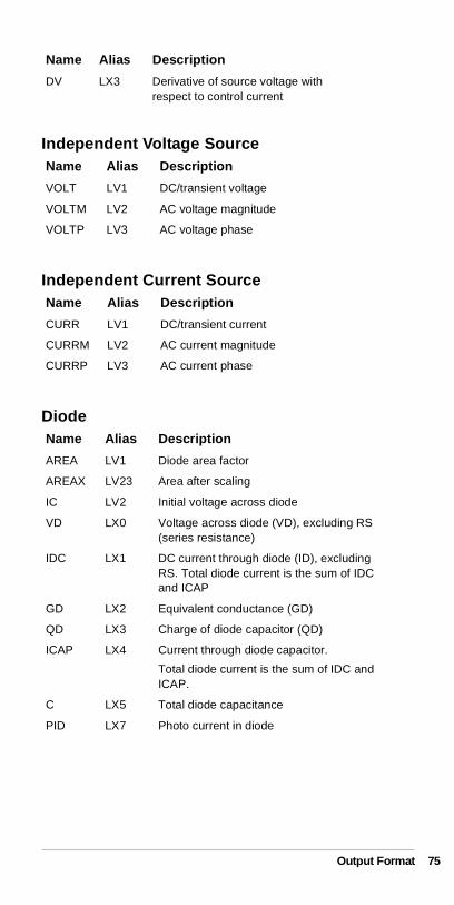
Independent Voltage Source
Independent Current Source
Diode
DV LX3 Derivative of source voltage with respect to control current
Name Alias Description
VOLT LV1 DC/transient voltage
VOLTM LV2 AC voltage magnitude
VOLTP LV3 AC voltage phase
Name Alias Description
CURR LV1 DC/transient current
CURRM LV2 AC current magnitude
CURRP LV3 AC current phase
Name Alias Description
AREA LV1 Diode area factor
AREAX LV23 Area after scaling
IC LV2 Initial voltage across diode
VD LX0 Voltage across diode (VD), excluding RS (series resistance)
IDC LX1 DC current through diode (ID), excluding RS. Total diode current is the sum of IDC and ICAP
GD LX2 Equivalent conductance (GD)
QD LX3 Charge of diode capacitor (QD)
ICAP LX4 Current through diode capacitor.
Total diode current is the sum of IDC and ICAP.
C LX5 Total diode capacitance
PID LX7 Photo current in diode
Name Alias Description
Output Format 75
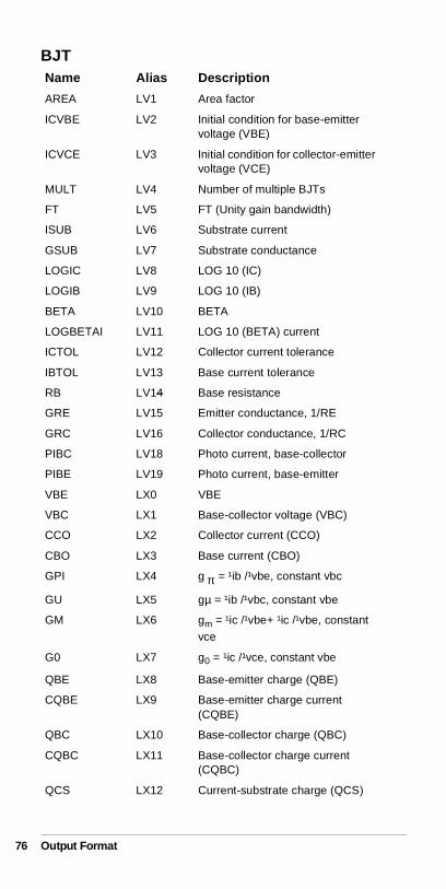
76
BJTName Alias Description
AREA LV1 Area factor
ICVBE LV2 Initial condition for base-emitter voltage (VBE)
ICVCE LV3 Initial condition for collector-emitter voltage (VCE)
MULT LV4 Number of multiple BJTs
FT LV5 FT (Unity gain bandwidth)
ISUB LV6 Substrate current
GSUB LV7 Substrate conductance
LOGIC LV8 LOG 10 (IC)
LOGIB LV9 LOG 10 (IB)
BETA LV10 BETA
LOGBETAI LV11 LOG 10 (BETA) current
ICTOL LV12 Collector current tolerance
IBTOL LV13 Base current tolerance
RB LV14 Base resistance
GRE LV15 Emitter conductance, 1/RE
GRC LV16 Collector conductance, 1/RC
PIBC LV18 Photo current, base-collector
PIBE LV19 Photo current, base-emitter
VBE LX0 VBE
VBC LX1 Base-collector voltage (VBC)
CCO LX2 Collector current (CCO)
CBO LX3 Base current (CBO)
GPI LX4 g = ¹ib /¹vbe, constant vbc
GU LX5 gµ = ¹ib /¹vbc, constant vbe
GM LX6 gm = ¹ic /¹vbe+ ¹ic /¹vbe, constant
vce
G0 LX7 g0 = ¹ic /¹vce, constant vbe
QBE LX8 Base-emitter charge (QBE)
CQBE LX9 Base-emitter charge current (CQBE)
QBC LX10 Base-collector charge (QBC)
CQBC LX11 Base-collector charge current (CQBC)
QCS LX12 Current-substrate charge (QCS)
π
Output Format
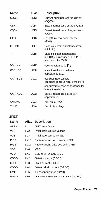
JFET
CQCS LX13 Current-substrate charge current (CQCS)
QBX LX14 Base-internal base charge (QBX)
CQBX LX15 Base-internal base charge current (CQBX)
GXO LX16 1/Rbeff Internal conductance (GXO)
CEXBC LX17 Base-collector equivalent current (CEXBC)
– LX18 Base-collector conductance (GEQCBO) (not used in HSPICE releases after 95.3)
CAP_BE LX19 cbe capacitance (C )
CAP_IBC LX20 cbc internal base-collector capacitance (Cµ)
CAP_SCB LX21 csc substrate-collector capacitance for vertical transistors
csb substrate-base capacitance for lateral transistors
CAP_XBC LX22 cbcx external base-collector capacitance
CMCMO LX23 ¹(TF*IBE) /¹vbc
VSUB LX24 Substrate voltage
Name Alias Description
AREA LV1 JFET area factor
VDS LV2 Initial drain-source voltage
VGS LV3 Initial gate-source voltage
PIGD LV16 Photo current, gate-drain in JFET
PIGS LV17 Photo current, gate-source in JFET
VGS LX0 VGS
VGD LX1 Gate-drain voltage (VGD)
CGSO LX2 Gate-to-source (CGSO)
CDO LX3 Drain current (CDO)
CGDO LX4 Gate-to-drain current (CGDO)
GMO LX5 Transconductance (GMO)
GDSO LX6 Drain-source transconductance (GDSO)
Name Alias Description
Π
Output Format 77
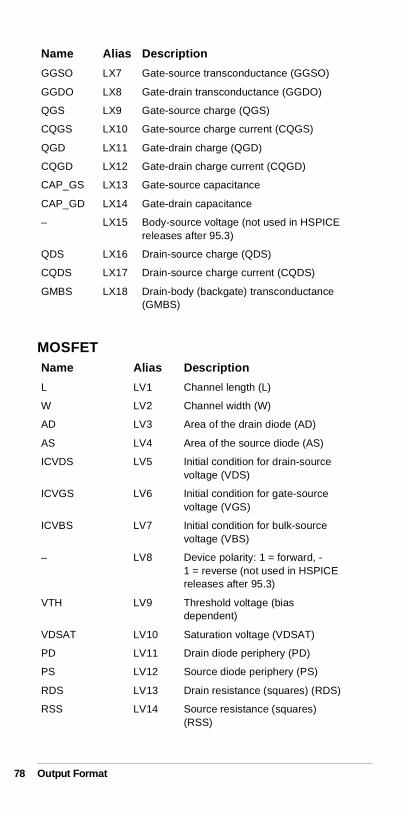
78
MOSFET
GGSO LX7 Gate-source transconductance (GGSO)
GGDO LX8 Gate-drain transconductance (GGDO)
QGS LX9 Gate-source charge (QGS)
CQGS LX10 Gate-source charge current (CQGS)
QGD LX11 Gate-drain charge (QGD)
CQGD LX12 Gate-drain charge current (CQGD)
CAP_GS LX13 Gate-source capacitance
CAP_GD LX14 Gate-drain capacitance
– LX15 Body-source voltage (not used in HSPICE releases after 95.3)
QDS LX16 Drain-source charge (QDS)
CQDS LX17 Drain-source charge current (CQDS)
GMBS LX18 Drain-body (backgate) transconductance (GMBS)
Name Alias Description
L LV1 Channel length (L)
W LV2 Channel width (W)
AD LV3 Area of the drain diode (AD)
AS LV4 Area of the source diode (AS)
ICVDS LV5 Initial condition for drain-source voltage (VDS)
ICVGS LV6 Initial condition for gate-source voltage (VGS)
ICVBS LV7 Initial condition for bulk-source voltage (VBS)
– LV8 Device polarity: 1 = forward, -1 = reverse (not used in HSPICE releases after 95.3)
VTH LV9 Threshold voltage (bias dependent)
VDSAT LV10 Saturation voltage (VDSAT)
PD LV11 Drain diode periphery (PD)
PS LV12 Source diode periphery (PS)
RDS LV13 Drain resistance (squares) (RDS)
RSS LV14 Source resistance (squares) (RSS)
Name Alias Description
Output Format
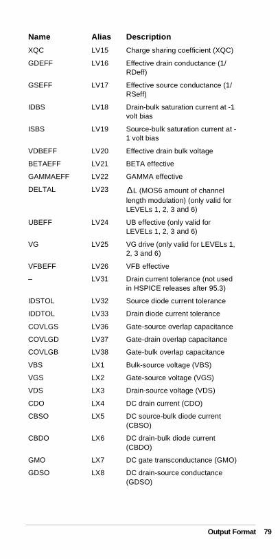
XQC LV15 Charge sharing coefficient (XQC)
GDEFF LV16 Effective drain conductance (1/RDeff)
GSEFF LV17 Effective source conductance (1/RSeff)
IDBS LV18 Drain-bulk saturation current at -1 volt bias
ISBS LV19 Source-bulk saturation current at -1 volt bias
VDBEFF LV20 Effective drain bulk voltage
BETAEFF LV21 BETA effective
GAMMAEFF LV22 GAMMA effective
DELTAL LV23 L (MOS6 amount of channel length modulation) (only valid for LEVELs 1, 2, 3 and 6)
UBEFF LV24 UB effective (only valid for LEVELs 1, 2, 3 and 6)
VG LV25 VG drive (only valid for LEVELs 1, 2, 3 and 6)
VFBEFF LV26 VFB effective
– LV31 Drain current tolerance (not used in HSPICE releases after 95.3)
IDSTOL LV32 Source diode current tolerance
IDDTOL LV33 Drain diode current tolerance
COVLGS LV36 Gate-source overlap capacitance
COVLGD LV37 Gate-drain overlap capacitance
COVLGB LV38 Gate-bulk overlap capacitance
VBS LX1 Bulk-source voltage (VBS)
VGS LX2 Gate-source voltage (VGS)
VDS LX3 Drain-source voltage (VDS)
CDO LX4 DC drain current (CDO)
CBSO LX5 DC source-bulk diode current (CBSO)
CBDO LX6 DC drain-bulk diode current (CBDO)
GMO LX7 DC gate transconductance (GMO)
GDSO LX8 DC drain-source conductance (GDSO)
Name Alias Description
∆
Output Format 79
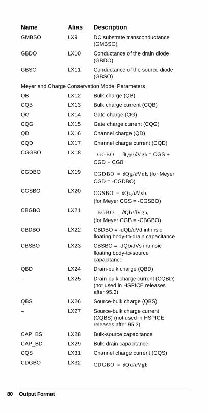
80
GMBSO LX9 DC substrate transconductance (GMBSO)
GBDO LX10 Conductance of the drain diode (GBDO)
GBSO LX11 Conductance of the source diode (GBSO)
Meyer and Charge Conservation Model Parameters
QB LX12 Bulk charge (QB)
CQB LX13 Bulk charge current (CQB)
QG LX14 Gate charge (QG)
CQG LX15 Gate charge current (CQG)
QD LX16 Channel charge (QD)
CQD LX17 Channel charge current (CQD)
CGGBO LX18 = CGS +
CGD + CGB
CGDBO LX19 , (for Meyer CGD = -CGDBO)
CGSBO LX20 ,
(for Meyer CGS = -CGSBO)
CBGBO LX21 ,
(for Meyer CGB = -CBGBO)
CBDBO LX22 CBDBO = -dQb/dVd intrinsic floating body-to-drain capacitance
CBSBO LX23 CBSBO = -dQb/dVs intrinsic floating body-to-source capacitance
QBD LX24 Drain-bulk charge (QBD)
– LX25 Drain-bulk charge current (CQBD) (not used in HSPICE releases after 95.3)
QBS LX26 Source-bulk charge (QBS)
– LX27 Source-bulk charge current (CQBS) (not used in HSPICE releases after 95.3)
CAP_BS LX28 Bulk-source capacitance
CAP_BD LX29 Bulk-drain capacitance
CQS LX31 Channel charge current (CQS)
CDGBO LX32
Name Alias Description
GGBO Qg/ Vgb∂∂=
CGDBO Qg/ Vdb∂∂=
CGSBO Qg/ Vsb∂∂=
BGBO Qb/ Vgb∂∂=
CDGBO Qd/ Vgb∂∂=
Output Format
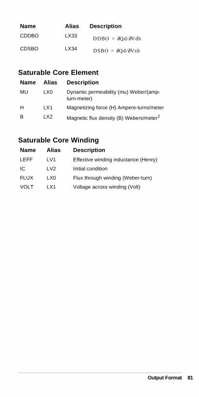
Saturable Core Element
Saturable Core Winding
CDDBO LX33
CDSBO LX34
Name Alias Description
MU LX0 Dynamic permeability (mu) Weber/(amp-turn-meter)
H LX1 Magnetizing force (H) Ampere-turns/meter
B LX2 Magnetic flux density (B) Webers/meter2
Name Alias Description
LEFF LV1 Effective winding inductance (Henry)
IC LV2 Initial condition
FLUX LX0 Flux through winding (Weber-turn)
VOLT LX1 Voltage across winding (Volt)
Name Alias Description
DDBO Qd/ Vdb∂∂=
DSBO Qd/ Vsb∂∂=
Output Format 81

82
Output Format