Hong Kong University of Science and Technology A 2-V...
143
Hong Kong University of Science and Technology A 2-V 900-MHz Monolithic CMOS Dual-Loop Frequency Synthesizer for GSM Receivers A thesis submitted to The Hong Kong University of Science and Technology in partial fulfillment of the requirements for the Degree of Master of Philosophy in Electrical and Electronic Engineering by Yan Shing Tak Department of Electrical and Electronic Engineering Bachelor of Engineering, HKUST 5th November 1999
-
Upload
dinhnguyet -
Category
Documents
-
view
216 -
download
0
Transcript of Hong Kong University of Science and Technology A 2-V...
Hong Kong University of Science and Technology
A 2-V 900-MHz Monolithic CMOS Dual-Loop Frequency
Synthesizer for GSM Receivers
A thesis submitted toThe Hong Kong University of Science and Technology
in partial fulfillment of the requirementsfor the Degree of Master of Philosophy in
Electrical and Electronic Engineering
by
Yan Shing Tak
Department of Electrical and Electronic Engineering
Bachelor of Engineering, HKUST
5th November 1999
A 2-V 900-MHz Monolithic CMOS Dual-Loop Frequency
Synthesizer for GSM Receivers
by
Yan Shing Tak
Approved by:
Dr. Howard C. LuongThesis Supervisor
Dr. W. H. KiThesis Examination Committee Member (Chairman)
Dr. K. T. MokThesis Examination Committee Member
Prof. Philip C. H. ChanHead of Department
Department of Electrical and Electronic Engineering
The Hong Kong University of Science and Technology
5th November 1999

A 2-V 900-MHz Monolithic CMOS Frequency Synthesizer for GSM Receiver
iii
Abstract
This master thesis presents the design of a 2-V 900-MHz monolithic CMOS dual-loop
frequency synthesizer for GSM receivers with good phase-noise performance.
Designing fully integrated frequency synthesizers for system integration is always
desirable but most challenging. This first requirement is to achieve high frequency operation
with reasonable power consumption. However, the most critical challenges for the frequency
synthesizer are the phase-noise and spurious-tone performance. Finally, small chip area is
essential to monolithic system integration.
The dual-loop design consists of two reference signals and two phase-locked loops
(PLLs) in cascode configuration. Because of the dual-loop architecture, input frequencies of the
two PLLs are scaled from 200 kHz to 1.6 MHz and 11.3 MHz. Therefore, the loop bandwidths
of both PLLs can be increased, so that both switching time and chip area can be reduced.
Implemented in a 0.5-µm CMOS technology and at 2-V supply voltage, the dual-loop
frequency synthesizer has a low power consumption of 34 mW. At 900 MHz, the phase noise
of the dual-loop design is less than -121.83 dBc/Hz at 600-kHz frequency offset. The spurious
tones are -79.5 [email protected], -82.0 [email protected] and -82.88 dBc@16MHz. The worst-case
switching time is less than 830µs. The chip area is 2.64 mm2. However, the peak close-in phase
noise is -65.67 dBc/Hz at 15-kHz frequency offset which is 15 dB worse than the specification
of GSM 900.

A 2-V 900-MHz Monolithic CMOS Frequency Synthesizer for GSM Receiver
iv
Acknowledgments
I would like to take this opportunity to express my gratitude to many individuals who
have given me a lot of supports during my master program in the HKUST.
First of all, I am indebted to my supervisor, Dr. Howard Luong, for his valuable
guidance and encouragement throughout the entire research. He has created an indispensable
environment with every support for me to conduct and enjoy my research work.
I would like to thank Frederick Kwok, Jack Chan, S. F. Luk, Joe Lai and Allen Ng for
their important technical supports in measurement setups and CAD tools. Special thanks to Rick
K. C. Mak and H. Y. Pang for his assistance in CAD and testing.
I would also be very grateful to my friends in analog research laboratory, device
characterization test laboratory, wireless communication laboratory and integrated power
electronics laboratory. They have shared their fun and experience with me from time to time.
Finally, I would like to thank Dr. W. H. Ki and Dr. K. T. Mok for being my thesis
examination committee and their helpful suggestions.

A 2-V 900-MHz Monolithic CMOS Frequency Synthesizer for GSM Receiver
v
Table of Contents
Chapter 1 Introduction. . . . . . . . . . . . . . . . . . . . . . . . . . . 1
1.1 Motivation: Single-Chip GSM Receiver . . . . . . . . . . . . . . . . . . . . . . . 1
1.2 Operating Principle of Phase-Locked Loop . . . . . . . . . . . . . . . . . . . . . 2
1.3 Problems of Single-Loop Frequency Synthesizer . . . . . . . . . . . . . . . . 3
1.3.1 Long Switching Time . . . . . . . . . . . . . . . . . . . . . . . . . . . . . . . . . . . . . . . . . . 3
1.3.2 Large Chip Area . . . . . . . . . . . . . . . . . . . . . . . . . . . . . . . . . . . . . . . . . . . . . . 3
1.3.3 Large Frequency-Division Ratio. . . . . . . . . . . . . . . . . . . . . . . . . . . . . . . . . . 3
1.4 Goals of the Project . . . . . . . . . . . . . . . . . . . . . . . . . . . . . . . . . . . . . . . 4
1.4.1 Higher Input Frequency . . . . . . . . . . . . . . . . . . . . . . . . . . . . . . . . . . . . . . . . 4
1.4.2 Lower Frequency-Division Ratio . . . . . . . . . . . . . . . . . . . . . . . . . . . . . . . . . 4
1.4.3 Lower Supply Voltage . . . . . . . . . . . . . . . . . . . . . . . . . . . . . . . . . . . . . . . . . 4
1.5 Thesis Overview. . . . . . . . . . . . . . . . . . . . . . . . . . . . . . . . . . . . . . . . . . 5
Chapter 2 Design Specification . . . . . . . . . . . . . . . . . . . . 6
2.1 Blocking Profile of GSM 900 . . . . . . . . . . . . . . . . . . . . . . . . . . . . . . . 6
2.2 Design-Specification Derivation . . . . . . . . . . . . . . . . . . . . . . . . . . . . . 7
2.2.1 Phase Noise. . . . . . . . . . . . . . . . . . . . . . . . . . . . . . . . . . . . . . . . . . . . . . . . . . 7
2.2.2 Spurious-Tone Specification. . . . . . . . . . . . . . . . . . . . . . . . . . . . . . . . . . . . 10
2.2.3 Switching Time. . . . . . . . . . . . . . . . . . . . . . . . . . . . . . . . . . . . . . . . . . . . . . 11
Chapter 3 Dual-Loop Frequency Synthesizer . . . . . . . 14
3.1 Architecture of Dual-Loop Design. . . . . . . . . . . . . . . . . . . . . . . . . . . 14
3.2 Advantages of the Dual-Loop Design . . . . . . . . . . . . . . . . . . . . . . . . 16
3.2.1 Smaller Chip Area and Faster Switching Time . . . . . . . . . . . . . . . . . . . . . 16
3.2.2 Simpler Programmable-Frequency-Divider Design . . . . . . . . . . . . . . . . . . 16
A 2-V 900-MHz Monolithic CMOS Frequency Synthesizer for GSM Receiver
vi
3.3 Potential Disadvantages of the Dual-Loop Design . . . . . . . . . . . . . . 16
3.3.1 Requirement of a Larger VCO-Tuning Range . . . . . . . . . . . . . . . . . . . . . . 16
3.3.2 Additional Chip area and Phase Noise . . . . . . . . . . . . . . . . . . . . . . . . . . . . 17
3.3.3 Long Switching Time . . . . . . . . . . . . . . . . . . . . . . . . . . . . . . . . . . . . . . . . . 17
3.3.4 Image-Output Frequency . . . . . . . . . . . . . . . . . . . . . . . . . . . . . . . . . . . . . . 17
3.3.5 Additional Design Effort. . . . . . . . . . . . . . . . . . . . . . . . . . . . . . . . . . . . . . . 18
Chapter 4 Circuit Implementation . . . . . . . . . . . . . . . . 19
4.1 Introduction . . . . . . . . . . . . . . . . . . . . . . . . . . . . . . . . . . . . . . . . . . . . 19
4.2 Voltage-Controlled Oscillator VCO2. . . . . . . . . . . . . . . . . . . . . . . . . 19
4.2.1 Design Requirement . . . . . . . . . . . . . . . . . . . . . . . . . . . . . . . . . . . . . . . . . . 19
4.2.2 Circuit Implementation . . . . . . . . . . . . . . . . . . . . . . . . . . . . . . . . . . . . . . . . 20
4.2.3 LC-Oscillator Analysis . . . . . . . . . . . . . . . . . . . . . . . . . . . . . . . . . . . . . . . . 21
4.2.3.1 Power Consumption . . . . . . . . . . . . . . . . . . . . . . . . . . . . . . . . . . . . . . . . 22
4.2.3.2 Oscillating Frequency . . . . . . . . . . . . . . . . . . . . . . . . . . . . . . . . . . . . . . 23
4.2.3.3 Phase Noise . . . . . . . . . . . . . . . . . . . . . . . . . . . . . . . . . . . . . . . . . . . . . . 24
4.2.4 Design of the On-Chip Spiral Inductor. . . . . . . . . . . . . . . . . . . . . . . . . . . . 26
4.2.4.1 Circular Spiral Inductor . . . . . . . . . . . . . . . . . . . . . . . . . . . . . . . . . . . . . 26
4.2.4.2 Minimum Metal Spacing . . . . . . . . . . . . . . . . . . . . . . . . . . . . . . . . . . . . 27
4.2.4.3 Limited Metal Width . . . . . . . . . . . . . . . . . . . . . . . . . . . . . . . . . . . . . . . 27
4.2.4.4 Hollow-Spiral Inductor . . . . . . . . . . . . . . . . . . . . . . . . . . . . . . . . . . . . . 27
4.2.4.5 Limited Inductor Area . . . . . . . . . . . . . . . . . . . . . . . . . . . . . . . . . . . . . . 28
4.2.4.6 Two-Layer Inductor . . . . . . . . . . . . . . . . . . . . . . . . . . . . . . . . . . . . . . . . 29
4.2.4.7 Inductor Simulation and Modelling . . . . . . . . . . . . . . . . . . . . . . . . . . . . 30
4.2.5 Design of the PN-Junction Varactor . . . . . . . . . . . . . . . . . . . . . . . . . . . . . . 31
4.2.5.1 Minimum Junction Spacing . . . . . . . . . . . . . . . . . . . . . . . . . . . . . . . . . . 31
4.2.5.2 Non-Minimum Junction Width . . . . . . . . . . . . . . . . . . . . . . . . . . . . . . . 31
4.2.6 Design and Optimization . . . . . . . . . . . . . . . . . . . . . . . . . . . . . . . . . . . . . . 33
4.3 Frequency divider N3. . . . . . . . . . . . . . . . . . . . . . . . . . . . . . . . . . . . . 36
4.3.1 Design Requirement . . . . . . . . . . . . . . . . . . . . . . . . . . . . . . . . . . . . . . . . . . 37
4.3.2 Circuit Implementation . . . . . . . . . . . . . . . . . . . . . . . . . . . . . . . . . . . . . . . . 38
4.3.2.1 The First Divide-by-2 Divider . . . . . . . . . . . . . . . . . . . . . . . . . . . . . . . . 38
4.3.2.2 The Second Divide-by-2 Divider . . . . . . . . . . . . . . . . . . . . . . . . . . . . . . 41
4.3.2.3 Single-to-Differential Converter . . . . . . . . . . . . . . . . . . . . . . . . . . . . . . 43
4.3.3 Design Parameters . . . . . . . . . . . . . . . . . . . . . . . . . . . . . . . . . . . . . . . . . . . 44
A 2-V 900-MHz Monolithic CMOS Frequency Synthesizer for GSM Receiver
vii
4.4 Down-Conversion Mixer . . . . . . . . . . . . . . . . . . . . . . . . . . . . . . . . . . 45
4.4.1 Design Requirement . . . . . . . . . . . . . . . . . . . . . . . . . . . . . . . . . . . . . . . . . . 45
4.4.2 Circuit Implementation . . . . . . . . . . . . . . . . . . . . . . . . . . . . . . . . . . . . . . . . 46
4.4.3 Design Issues . . . . . . . . . . . . . . . . . . . . . . . . . . . . . . . . . . . . . . . . . . . . . . . 47
4.5 Voltage-Controlled Oscillator VCO1. . . . . . . . . . . . . . . . . . . . . . . . . 48
4.5.1 Design Requirement . . . . . . . . . . . . . . . . . . . . . . . . . . . . . . . . . . . . . . . . . . 48
4.5.2 Circuit Implementation . . . . . . . . . . . . . . . . . . . . . . . . . . . . . . . . . . . . . . . . 48
4.5.2.1 High Frequency Operation. . . . . . . . . . . . . . . . . . . . . . . . . . . . . . . . . . . 49
4.5.2.2 Wide Frequency-Tuning Range . . . . . . . . . . . . . . . . . . . . . . . . . . . . . . . 49
4.5.2.3 Low Phase-Noise Performance . . . . . . . . . . . . . . . . . . . . . . . . . . . . . . . 50
4.5.3 Ring-Oscillator Analysis. . . . . . . . . . . . . . . . . . . . . . . . . . . . . . . . . . . . . . . 51
4.5.3.1 Operating-Frequency Range . . . . . . . . . . . . . . . . . . . . . . . . . . . . . . . . . 51
4.5.3.2 Phase-Noise Analysis. . . . . . . . . . . . . . . . . . . . . . . . . . . . . . . . . . . . . . . 52
4.5.4 Design Optimization . . . . . . . . . . . . . . . . . . . . . . . . . . . . . . . . . . . . . . . . . . 53
4.6 Frequency Divider N2 . . . . . . . . . . . . . . . . . . . . . . . . . . . . . . . . . . . . 56
4.6.1 Design Requirement . . . . . . . . . . . . . . . . . . . . . . . . . . . . . . . . . . . . . . . . . . 56
4.6.2 Circuit implementation . . . . . . . . . . . . . . . . . . . . . . . . . . . . . . . . . . . . . . . . 56
4.7 Programmable-Frequency Divider N1 . . . . . . . . . . . . . . . . . . . . . . . . 57
4.7.1 Design Requirement . . . . . . . . . . . . . . . . . . . . . . . . . . . . . . . . . . . . . . . . . . 57
4.7.2 Circuit Implementation . . . . . . . . . . . . . . . . . . . . . . . . . . . . . . . . . . . . . . . . 58
4.7.3 System-Design Optimization . . . . . . . . . . . . . . . . . . . . . . . . . . . . . . . . . . . 59
4.7.4 Dual-Modulus Prescaler . . . . . . . . . . . . . . . . . . . . . . . . . . . . . . . . . . . . . . . 60
4.7.4.1 Operation . . . . . . . . . . . . . . . . . . . . . . . . . . . . . . . . . . . . . . . . . . . . . . . . 60
4.7.4.2 Circuit Implementation . . . . . . . . . . . . . . . . . . . . . . . . . . . . . . . . . . . . . 62
4.7.5 P and S Counters. . . . . . . . . . . . . . . . . . . . . . . . . . . . . . . . . . . . . . . . . . . . . 65
4.7.5.1 Operation . . . . . . . . . . . . . . . . . . . . . . . . . . . . . . . . . . . . . . . . . . . . . . . . 65
4.7.5.2 Circuit Implementation of the P and S Counters . . . . . . . . . . . . . . . . . . 66
4.7.6 Simulation Results . . . . . . . . . . . . . . . . . . . . . . . . . . . . . . . . . . . . . . . . . . . 67
4.8 Phase-Frequency Detector PDF1 & PFD2. . . . . . . . . . . . . . . . . . . . . 68
4.8.1 Design Requirement . . . . . . . . . . . . . . . . . . . . . . . . . . . . . . . . . . . . . . . . . . 68
4.8.2 Circuit Implementation . . . . . . . . . . . . . . . . . . . . . . . . . . . . . . . . . . . . . . . . 69
4.8.3 Design and Simulation . . . . . . . . . . . . . . . . . . . . . . . . . . . . . . . . . . . . . . . . 71
4.9 Charge Pumps and Loop Filters . . . . . . . . . . . . . . . . . . . . . . . . . . . . . 72
4.9.1 Design Requirement . . . . . . . . . . . . . . . . . . . . . . . . . . . . . . . . . . . . . . . . . . 72
4.9.2 Circuit Implementation . . . . . . . . . . . . . . . . . . . . . . . . . . . . . . . . . . . . . . . . 73
A 2-V 900-MHz Monolithic CMOS Frequency Synthesizer for GSM Receiver
viii
4.9.2.1 Charge Pumps CP1 & CP2 . . . . . . . . . . . . . . . . . . . . . . . . . . . . . . . . . . 73
4.9.2.2 Loop-Filter Implementation LF1 & LF2 . . . . . . . . . . . . . . . . . . . . . . . . 74
4.9.3 Frequency-Synthesizer Modelling . . . . . . . . . . . . . . . . . . . . . . . . . . . . . . . 76
4.9.4 Spurious-Tone Analysis . . . . . . . . . . . . . . . . . . . . . . . . . . . . . . . . . . . . . . . 78
4.9.4.1 Current Mismatch. . . . . . . . . . . . . . . . . . . . . . . . . . . . . . . . . . . . . . . . . . 78
4.9.4.2 Switch Clock Feed Through and Charge Injection . . . . . . . . . . . . . . . . 81
4.9.4.3 Charge Sharing. . . . . . . . . . . . . . . . . . . . . . . . . . . . . . . . . . . . . . . . . . . . 82
4.9.4.4 Total Spurious-Tone Performance . . . . . . . . . . . . . . . . . . . . . . . . . . . . . 85
4.9.4.5 Spurious-Tone Optimization . . . . . . . . . . . . . . . . . . . . . . . . . . . . . . . . . 85
4.9.5 Phase-Noise Analysis . . . . . . . . . . . . . . . . . . . . . . . . . . . . . . . . . . . . . . . . . 85
4.9.5.1 Charge-Pump and Loop-Filter Phase Noise. . . . . . . . . . . . . . . . . . . . . . 86
4.9.5.2 Voltage-Controlled Oscillator Phase Noise . . . . . . . . . . . . . . . . . . . . . . 88
4.9.5.3 Frequency-Synthesizer Phase Noise . . . . . . . . . . . . . . . . . . . . . . . . . . . 89
4.9.5.4 Phase-noise optimization . . . . . . . . . . . . . . . . . . . . . . . . . . . . . . . . . . . . 89
4.9.6 Loop Stability Consideration . . . . . . . . . . . . . . . . . . . . . . . . . . . . . . . . . . . 90
4.9.7 Charge-Pump and Loop-Filter Design Optimization . . . . . . . . . . . . . . . . . 93
4.9.7.1 Design Consideration . . . . . . . . . . . . . . . . . . . . . . . . . . . . . . . . . . . . . . . 93
4.9.7.2 High-Frequency Loop Design . . . . . . . . . . . . . . . . . . . . . . . . . . . . . . . . 93
4.9.7.3 Low-Frequency Loop Design . . . . . . . . . . . . . . . . . . . . . . . . . . . . . . . . 95
4.9.8 Performance Summary of the Dual-Loop Frequency Synthesizer . . . . . . . 97
Chapter 5 Layout . . . . . . . . . . . . . . . . . . . . . . . . . . . . . . 99
5.1 Introduction . . . . . . . . . . . . . . . . . . . . . . . . . . . . . . . . . . . . . . . . . . . . 99
5.2 Loop-Filter Capacitor Layout. . . . . . . . . . . . . . . . . . . . . . . . . . . . . . . 99
5.3 VCO-Inductor Layout . . . . . . . . . . . . . . . . . . . . . . . . . . . . . . . . . . . 100
5.4 Supply-Line and Pad Layout . . . . . . . . . . . . . . . . . . . . . . . . . . . . . . 101
5.5 Layout of the Dual-Loop Frequency Synthesizer . . . . . . . . . . . . . . 102
Chapter 6 Measurement . . . . . . . . . . . . . . . . . . . . . . . . 105
6.1 Introduction . . . . . . . . . . . . . . . . . . . . . . . . . . . . . . . . . . . . . . . . . . . 105
6.2 LC Oscillator VCO2. . . . . . . . . . . . . . . . . . . . . . . . . . . . . . . . . . . . . 105
6.2.1 Spiral Inductor & PN-Junction Varactor . . . . . . . . . . . . . . . . . . . . . . . . . 105
6.2.1.1 Test Setup. . . . . . . . . . . . . . . . . . . . . . . . . . . . . . . . . . . . . . . . . . . . . . . 105
6.2.1.2 Measurement Results of Spiral Inductor . . . . . . . . . . . . . . . . . . . . . . . 106
A 2-V 900-MHz Monolithic CMOS Frequency Synthesizer for GSM Receiver
ix
6.2.1.3 Measurement Results of PN-Junction Varactor . . . . . . . . . . . . . . . . . . 109
6.2.2 LC oscillator . . . . . . . . . . . . . . . . . . . . . . . . . . . . . . . . . . . . . . . . . . . . . . . 110
6.2.2.1 Test Setup for Phase-Noise Measurement . . . . . . . . . . . . . . . . . . . . . . 110
6.2.2.2 Phase-Noise Measurement Results . . . . . . . . . . . . . . . . . . . . . . . . . . . 111
6.3 Ring Oscillator VCO1 . . . . . . . . . . . . . . . . . . . . . . . . . . . . . . . . . . . 112
6.4 Frequency Dividers N1, N2 & N3 . . . . . . . . . . . . . . . . . . . . . . . . . . 113
6.4.1 Frequency Divider N1. . . . . . . . . . . . . . . . . . . . . . . . . . . . . . . . . . . . . . . . 113
6.4.2 Frequency Divider N2. . . . . . . . . . . . . . . . . . . . . . . . . . . . . . . . . . . . . . . . 114
6.4.3 Frequency Divider N3. . . . . . . . . . . . . . . . . . . . . . . . . . . . . . . . . . . . . . . . 115
6.5 Dual-Loop Frequency Synthesizer . . . . . . . . . . . . . . . . . . . . . . . . . . 116
6.5.1 Loop Filters. . . . . . . . . . . . . . . . . . . . . . . . . . . . . . . . . . . . . . . . . . . . . . . . 116
6.5.2 Spurious Tones . . . . . . . . . . . . . . . . . . . . . . . . . . . . . . . . . . . . . . . . . . . . . 117
6.5.3 Phase Noise. . . . . . . . . . . . . . . . . . . . . . . . . . . . . . . . . . . . . . . . . . . . . . . . 119
6.5.4 Switching Time. . . . . . . . . . . . . . . . . . . . . . . . . . . . . . . . . . . . . . . . . . . . . 120
6.5.4.1 Test Setup for Switching-Time Measurement . . . . . . . . . . . . . . . . . . . 120
6.5.4.2 Switching-Time Measurement Results . . . . . . . . . . . . . . . . . . . . . . . . 121
6.6 Performance Comparison . . . . . . . . . . . . . . . . . . . . . . . . . . . . . . . . . 122
Chapter 7 Conclusion . . . . . . . . . . . . . . . . . . . . . . . . . . 125
A 2-V 900-MHz Monolithic CMOS Frequency Synthesizer for GSM Receiver
x
List of Figures
Figure 1.1 Block diagram of the GSM receiver front-end. . . . . . . . . . . . . . . . . . . . . . . . . . 1
Figure 1.2 Block diagram of the single-loop frequency synthesizer. . . . . . . . . . . . . . . . . . 2
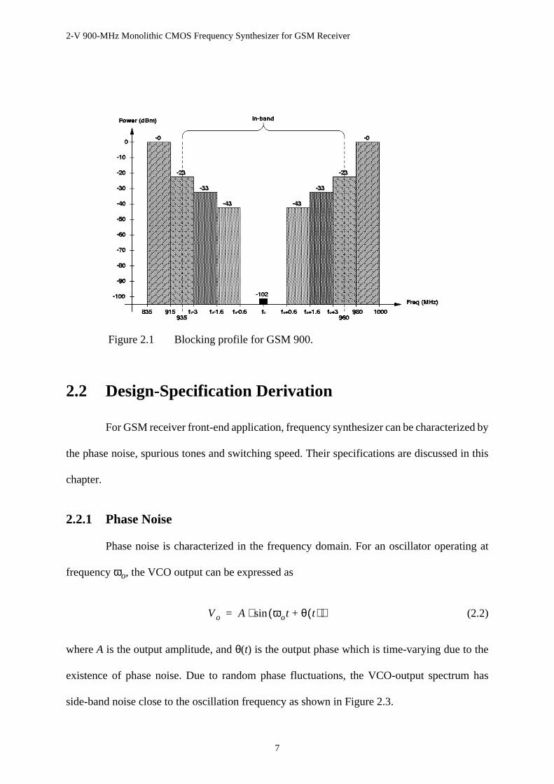
Figure 2.1 Blocking profile for GSM 900. . . . . . . . . . . . . . . . . . . . . . . . . . . . . . . . . . . . . . 7
Figure 2.3 Degradation of SNR due to phase noise. . . . . . . . . . . . . . . . . . . . . . . . . . . . . . . 9
Figure 2.5 Degradation of SNR due to spurious tone. . . . . . . . . . . . . . . . . . . . . . . . . . . . 11
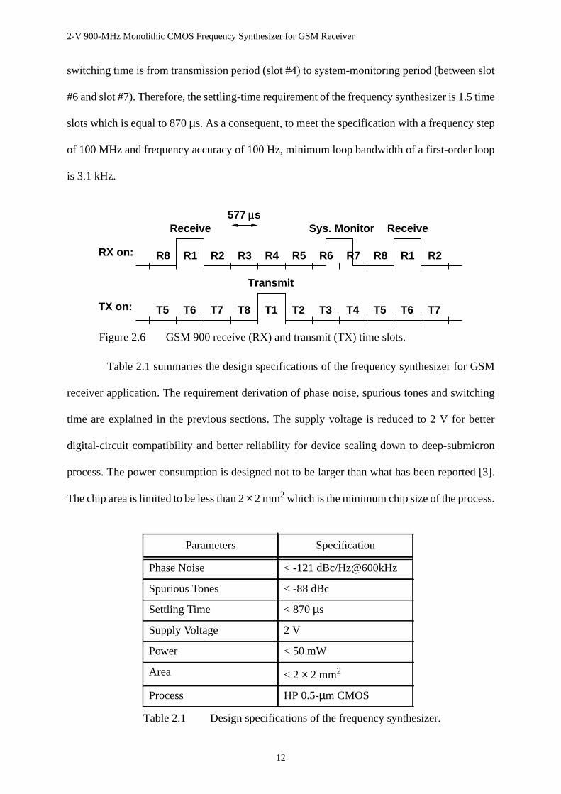
Figure 2.6 GSM 900 receive (RX) and transmit (TX) time slots. . . . . . . . . . . . . . . . . . . 12
Figure 3.1 Block diagrams of the proposed dual-loop frequency synthesizer.. . . . . . . . . 14
Figure 4.1 Location of the LC-oscillator VCO2. . . . . . . . . . . . . . . . . . . . . . . . . . . . . . . . 20
Figure 4.2 Circuit implementation of the LC-oscillator VCO2. . . . . . . . . . . . . . . . . . . . . 21
Figure 4.3 Another possible implementation of the LC-oscillator. . . . . . . . . . . . . . . . . . 21
Figure 4.4 Linear circuit model of the LC tank. . . . . . . . . . . . . . . . . . . . . . . . . . . . . . . . . 22
Figure 4.5 Time-variant phenomenon of the LC-oscillator. . . . . . . . . . . . . . . . . . . . . . . . 25
Figure 4.6 Generation of eddy currents in spiral inductor. . . . . . . . . . . . . . . . . . . . . . . . . 28
Figure 4.7 Generation of substrate currents on spiral inductors. . . . . . . . . . . . . . . . . . . . 29
Figure 4.8 On-chip spiral inductor model in ASITIC. . . . . . . . . . . . . . . . . . . . . . . . . . . . 30
Figure 4.9 Cross-section and circuit model of pn-junction varactor. . . . . . . . . . . . . . . . . 31
Figure 4.10 Measurement results of two pn-junction varactors with different junction width(a) 6.6 mm and (b) 1.5 mm.. . . . . . . . . . . . . . . . . . . . . . . . . . . . . . . . . . . . . . . 32
Figure 4.11 Phase-noise and power-consumption optimization of the LC-oscillator. . . . . 34
Figure 4.12 Oscillating frequency, single-ended peak-to-peak output amplitude and VCOgain of the LC oscillator. . . . . . . . . . . . . . . . . . . . . . . . . . . . . . . . . . . . . . . . . . 36
Figure 4.13 Phase-noise simulation results of the LC oscillator by SpectreRF.. . . . . . . . . 36
Figure 4.14 Location of the frequency divider N3.. . . . . . . . . . . . . . . . . . . . . . . . . . . . . . . 37
Figure 4.15 Cascade configuration of the frequency divider N3. . . . . . . . . . . . . . . . . . . . . 38
Figure 4.16 The first divide-by-2 frequency divider of divider N3. . . . . . . . . . . . . . . . . . . 39
Figure 4.17 The operation of the pseudo-NMOS divide-by-two divider in (a) prechargephase and (b) evaluation phase. . . . . . . . . . . . . . . . . . . . . . . . . . . . . . . . . . . . . 40
Figure 4.18 True-Single-Phase-Clock (TSPC) divide-by-2 frequency divider. . . . . . . . . . 41
Figure 4.19 Operation of the TSPC divider in (a) hold mode and (b) evaluation mode. . . 42
Figure 4.20 Timing requirement of a TSPC divide-by-2 divider. . . . . . . . . . . . . . . . . . . . 43
Figure 4.21 Circuit schematic of the single-to-differential converter. . . . . . . . . . . . . . . . . 43
A 2-V 900-MHz Monolithic CMOS Frequency Synthesizer for GSM Receiver
xi
Figure 4.22 Simulation results of the whole frequency divider N3. . . . . . . . . . . . . . . . . . . 45
Figure 4.23 Location of the down-conversion mixer.. . . . . . . . . . . . . . . . . . . . . . . . . . . . . 46
Figure 4.24 Circuit implementation of the down-conversion mixer. . . . . . . . . . . . . . . . . . 47
Figure 4.25 Location of the voltage-controlled oscillator VCO1. . . . . . . . . . . . . . . . . . . . 48
Figure 4.26 Schematics of (a) delay cell and (b) ring oscillator. . . . . . . . . . . . . . . . . . . . . 49
Figure 4.27 Delay cell waveforms and corresponding thermal noise current. . . . . . . . . . . 50
Figure 4.28 Half circuit of the delay cell for operating frequency analysis.. . . . . . . . . . . . 51
Figure 4.29 Approximate ISF for the ring-oscillator phase-noise analysis. . . . . . . . . . . . . 53
Figure 4.30 Design optimization of the ring oscillator VCO1.. . . . . . . . . . . . . . . . . . . . . . 54
Figure 4.31 Operating frequency, VCO gain and power consumption of the ring oscillatorVCO2. . . . . . . . . . . . . . . . . . . . . . . . . . . . . . . . . . . . . . . . . . . . . . . . . . . . . . . . 55
Figure 4.32 Phase-noise performance of the ring oscillator VCO2.. . . . . . . . . . . . . . . . . . 55
Figure 4.33 Location of the divide-by-32 frequency divider N2. . . . . . . . . . . . . . . . . . . . . 56
Figure 4.34 Transient simulation of the divide-by-32 frequency divider N2. . . . . . . . . . . 57
Figure 4.35 Location of the programmable frequency divider N1. . . . . . . . . . . . . . . . . . . 58
Figure 4.36 Implementation of the programmable-frequency divider N1.. . . . . . . . . . . . . 58
Figure 4.37 Circuit implementation of the dual-modulus prescaler: . . . . . . . . . . . . . . . . . 61
Figure 4.38 Relaxed timing requirement of the back-carrier-propagation approach.. . . . . 61
Figure 4.39 Circuit implementation with “000” detection.. . . . . . . . . . . . . . . . . . . . . . . . . 62
Figure 4.40 Circuit implementation of the divide-by-3 frequency divider DIV3. . . . . . . . 63
Figure 4.41 Circuit implementation of the NOR-gate-embedded D-flip-flop NORDFF. . 63
Figure 4.42 Transient simulation of the dual-modulus prescaler at 700 MHz. . . . . . . . . . 65
Figure 4.43 Circuit implementation of the (a) P counter and (b) S counter. . . . . . . . . . . . 66
Figure 4.44 Circuit implementation of the loadable TSPC D-flip-flops for both P and Scounters.. . . . . . . . . . . . . . . . . . . . . . . . . . . . . . . . . . . . . . . . . . . . . . . . . . . . . . 67
Figure 4.45 Transient simulation of the programmable-frequency divider N1 = 349.. . . . 68
Figure 4.46 Location of the Phase-Frequency Detectors PFD1 & PFD2. . . . . . . . . . . . . . 69
Figure 4.47 The effect of (a) PFD transfer function and (b) close-in phase noise of the PFDwith/without dead zone.. . . . . . . . . . . . . . . . . . . . . . . . . . . . . . . . . . . . . . . . . . 69
Figure 4.48 PFD implementation: (a) block diagram and (b) operation. . . . . . . . . . . . . . . 70
Figure 4.49 Implementation of the TSPC half-transparent D-flip-flop of the PFDs. . . . . . 70
Figure 4.50 Simulation results of the PFDs at 2 MHz. . . . . . . . . . . . . . . . . . . . . . . . . . . . . 72
Figure 4.51 Location of the charge-pumps CP1 & CP2, and loop filters LF1 & LF2.. . . . 73
Figure 4.52 Circuit implementation of the charge pumps CP1 & CP2. . . . . . . . . . . . . . . . 74
Figure 4.53 Circuit implementation of the loop filters LF1 & LF2. . . . . . . . . . . . . . . . . . . 75
Figure 4.54 Linear capacitor for loop-filter-capacitor implementation C1 & C2: (a) devicestructure and (b) circuit model. . . . . . . . . . . . . . . . . . . . . . . . . . . . . . . . . . . . . 75
Figure 4.55 Linear model of the dual-loop frequency synthesizer. . . . . . . . . . . . . . . . . . . 76

A 2-V 900-MHz Monolithic CMOS Frequency Synthesizer for GSM Receiver
xii
Figure 4.56 Charge-pump current-injection mismatch: (a) cause, (b) transient response, and(c) frequency response. . . . . . . . . . . . . . . . . . . . . . . . . . . . . . . . . . . . . . . . . . . 79
Figure 4.57 Current-mismatch analysis of a current mirror.. . . . . . . . . . . . . . . . . . . . . . . . 79
Figure 4.58 Effect of clock feed through and charge injection of switches on the spurious-tone performance. . . . . . . . . . . . . . . . . . . . . . . . . . . . . . . . . . . . . . . . . . . . . . . 81
Figure 4.59 Effect of charge sharing: (a) SW1b & SW2b are on and (b) SW1a & SW2a areon. . . . . . . . . . . . . . . . . . . . . . . . . . . . . . . . . . . . . . . . . . . . . . . . . . . . . . . . . . . 83
Figure 4.60 Small-signal model for the phase-noise analysis of the charge-pumps and loopfilters. . . . . . . . . . . . . . . . . . . . . . . . . . . . . . . . . . . . . . . . . . . . . . . . . . . . . . . . . 86
Figure 4.61 Bode plot of the open-loop transfer function. . . . . . . . . . . . . . . . . . . . . . . . . . 91
Figure 4.62 The variation of the loop bandwidth fu and phase margin PM of the high-frequency loop due to the VCO-gain variation of the LC-oscillator VCO2. . 94
Figure 4.63 Design optimization of the charge pump and loop filter of the high-frequencyloop. . . . . . . . . . . . . . . . . . . . . . . . . . . . . . . . . . . . . . . . . . . . . . . . . . . . . . . . . . 94
Figure 4.64 The variation of the loop bandwidth fu and phase margin PM of the low-frequency loop due the VCO-gain variation of the ring oscillator VCO1. . . . 95
Figure 4.65 Design optimization of the charge pump and loop filter of the low-frequencyloop. . . . . . . . . . . . . . . . . . . . . . . . . . . . . . . . . . . . . . . . . . . . . . . . . . . . . . . . . . 96
Figure 4.66 Phase noise of the whole dual-loop frequency synthesizer. . . . . . . . . . . . . . . 97
Figure 5.1 Layout of the loop-filter capacitors. . . . . . . . . . . . . . . . . . . . . . . . . . . . . . . . 100
Figure 5.2 Layout of the VCO on-chip spiral inductor. . . . . . . . . . . . . . . . . . . . . . . . . . 101
Figure 5.3 Noise de-coupling filter of the analog and digital supplies. . . . . . . . . . . . . . 102
Figure 5.4 Floor plan of the dual-loop frequency synthesizer. . . . . . . . . . . . . . . . . . . . . 103
Figure 5.5 Layout of the dual-loop frequency synthesizer. . . . . . . . . . . . . . . . . . . . . . . 104
Figure 6.1 Measurement setup for the passive components. . . . . . . . . . . . . . . . . . . . . . 106
Figure 6.2 Measurement results and model of the on-chip spiral inductor which is used inthe LC oscillator. . . . . . . . . . . . . . . . . . . . . . . . . . . . . . . . . . . . . . . . . . . . . . . 107
Figure 6.3 Measurement results of the inductor test structures with laminated N-well,laminated polysilicon and only P-substrate under the inductors. . . . . . . . . . 108
Figure 6.4 Measurement results and biasing condition of the pn-junction varactor. . . . 110
Figure 6.5 Test setup for the phase-noise measurement. . . . . . . . . . . . . . . . . . . . . . . . . 111
Figure 6.6 Measurement results of the LC oscillator VCO2. . . . . . . . . . . . . . . . . . . . . . 112
Figure 6.7 Measurement results of the ring oscillator VCO1. . . . . . . . . . . . . . . . . . . . . 113
Figure 6.8 Output waveforms of the programmable-frequency divider N1 at 600 MHz with(a) N1 = 226 and (b) N1 = 349. . . . . . . . . . . . . . . . . . . . . . . . . . . . . . . . . . . . 114
Figure 6.9 Waveforms of the divide-by-32 frequency divider N2 at 600 MHz. . . . . . . 115
Figure 6.10 Waveforms of the divide-by-4 frequency divider N3 operating at 1 GHz. . . 116
Figure 6.11 Measurement results of the loop-filter impedance of the (a) low-frequency loopand (b) high-frequency loop. . . . . . . . . . . . . . . . . . . . . . . . . . . . . . . . . . . . . . 117
Figure 6.12 Measurement results of the spurious tones at fo = 865.2 MHz. . . . . . . . . . . 118

A 2-V 900-MHz Monolithic CMOS Frequency Synthesizer for GSM Receiver
xiii
Figure 6.13 Spurious level at 1.6 MHz when the low-frequency loop is turned off. . . . . 119
Figure 6.14 Measurement results of the phase noise at fo = 889.8 MHz.. . . . . . . . . . . . . 120
Figure 6.15 Measurement setup for the switching-time measurement. . . . . . . . . . . . . . . 121
Figure 6.16 VCO control voltages of the low-frequency and high-frequency loops switchingbetween the minimum and maximum channels. . . . . . . . . . . . . . . . . . . . . . . 122
A 2-V 900-MHz Monolithic CMOS Frequency Synthesizer for GSM Receiver
xiv
List of Tables
Table 2.1 Design specifications of the frequency synthesizer. . . . . . . . . . . . . . . . . . . . . 12
Table 4.1 Simulated inductor parameters applied to the LC-oscillator optimization.. . . 33
Table 4.2 Design parameters of the LC oscillator. . . . . . . . . . . . . . . . . . . . . . . . . . . . . . 35
Table 4.3 Design parameters of the frequency divider N3. . . . . . . . . . . . . . . . . . . . . . . . 44
Table 4.4 Design parameters of the down-conversion mixer. . . . . . . . . . . . . . . . . . . . . . 47
Table 4.5 Design parameters of the ring oscillator VCO1. . . . . . . . . . . . . . . . . . . . . . . . 54
Table 4.6 Design parameters of the divide-by-32 frequency divider N2. . . . . . . . . . . . . 57
Table 4.7 System design optimization of the programmable frequency divider N1. . . . 60
Table 4.8 Design parameters of the dual-modulus prescaler. . . . . . . . . . . . . . . . . . . . . . 64
Table 4.9 Design parameters of the PFDs. . . . . . . . . . . . . . . . . . . . . . . . . . . . . . . . . . . . 71
Table 4.10 Design parameters of the high-frequency loop.. . . . . . . . . . . . . . . . . . . . . . . . 95
Table 4.11 Design parameters of the charge pump and loop filter of the low -frequencyloop. . . . . . . . . . . . . . . . . . . . . . . . . . . . . . . . . . . . . . . . . . . . . . . . . . . . . . . . . . 97
Table 4.12 Performance summary of the dual-loop frequency synthesizer. . . . . . . . . . . . 98
Table 6.1 Performance comparison between different monolithic implementation of thefrequency synthesizer. . . . . . . . . . . . . . . . . . . . . . . . . . . . . . . . . . . . . . . . . . . 124
A 2-V 900-MHz Monolithic CMOS Frequency Synthesizer for GSM Receiver
1
Chapter 1
Introduction
1.1 Motivation: Single-Chip GSM Receiver
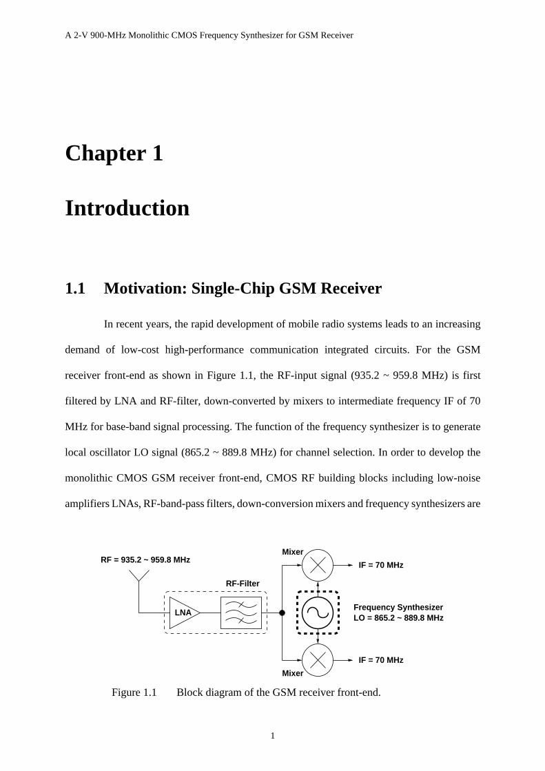
In recent years, the rapid development of mobile radio systems leads to an increasing
demand of low-cost high-performance communication integrated circuits. For the GSM
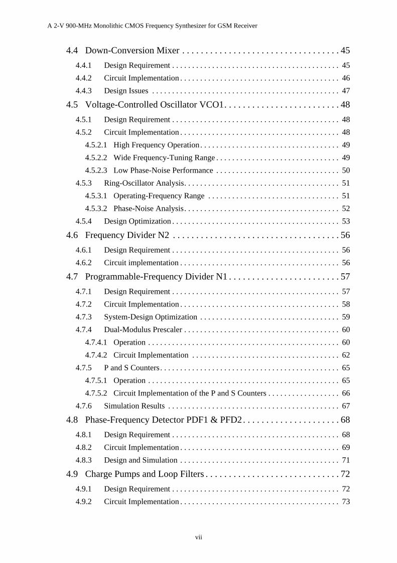
receiver front-end as shown in Figure 1.1, the RF-input signal (935.2 ~ 959.8 MHz) is first
filtered by LNA and RF-filter, down-converted by mixers to intermediate frequency IF of 70
MHz for base-band signal processing. The function of the frequency synthesizer is to generate
local oscillator LO signal (865.2 ~ 889.8 MHz) for channel selection. In order to develop the
monolithic CMOS GSM receiver front-end, CMOS RF building blocks including low-noise
amplifiers LNAs, RF-band-pass filters, down-conversion mixers and frequency synthesizers are
RF-Filter
LNA
IF = 70 MHz
LO = 865.2 ~ 889.8 MHzFrequency Synthesizer
Mixer
Mixer
IF = 70 MHz
RF = 935.2 ~ 959.8 MHz
Figure 1.1 Block diagram of the GSM receiver front-end.

2-V 900-MHz Monolithic CMOS Frequency Synthesizer for GSM Receiver
2
needed. However, despite of much progress in designing LNAs [1] and mixers [2], only little
results on frequency synthesizers that meet GSM specifications have been reported [3].
1.2 Operating Principle of Phase-Locked Loop
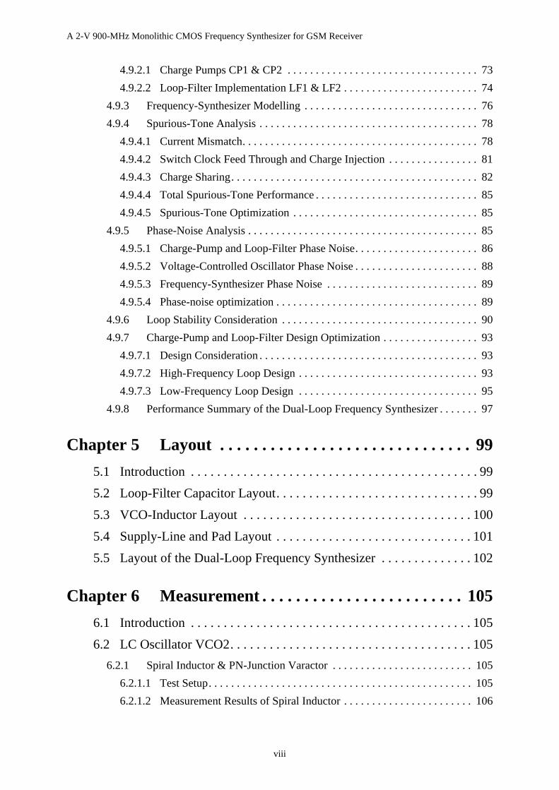
Phase-Locked Loop PLL is a circuit in which the phase of a local oscillator is locked
to the phase of an external signal. As shown in Figure 1.2, PLL consists of a crystal oscillator
XTAL, a phase-frequency detector PFD, a charge pump CP, a loop filter LF, a
voltage-controlled oscillator VCO, and a programmable frequency divider. Crystal oscillator
aims to provide an accurate and clean input reference signal to the frequency synthesizer. Then,
phase-frequency detector compares the phase and frequency difference between the reference
signal and the output signal of programmable frequency divider. According to the phase and
frequency difference, the charge pump injects appropriate current to adjust the control voltage
of the VCO. The loop filter filters out the high frequency components and extracts the average
VCO control voltage to improve the spectral purity of the VCO output. The VCO is adjusted by
the loop so that phase of VCO and that of input reference become matched. In order to program
the output frequency at desired channels (865.2 ~ 889.8 MHz) with a fixed input reference (200
kHz), a programmable frequency divider (N = 4326 ~ 4449) is included in the feedback path.
f ch = 200kHz
Vc
f o = 865.2 ~ 889.8MHz
PFD CP
LF VCOUP
DN
XTAL
1/N
N = 4326 ~ 4449
Figure 1.2 Block diagram of the single-loop frequency synthesizer.
2-V 900-MHz Monolithic CMOS Frequency Synthesizer for GSM Receiver
3
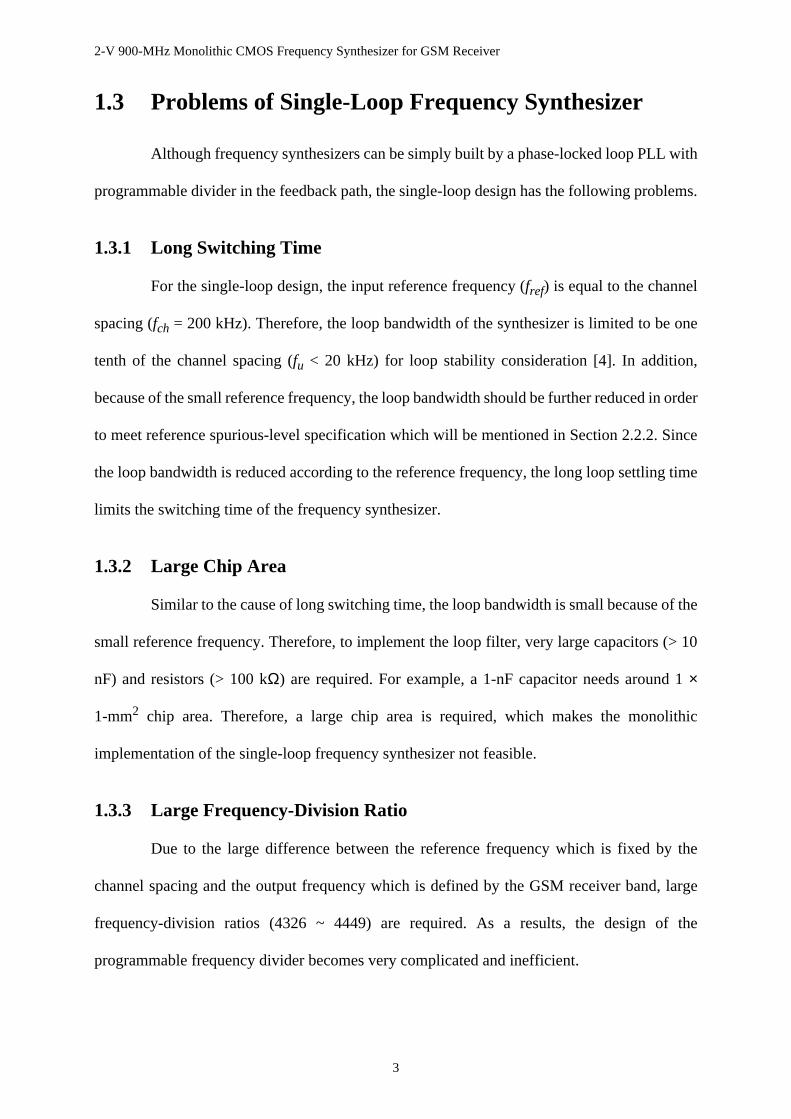
1.3 Problems of Single-Loop Frequency Synthesizer
Although frequency synthesizers can be simply built by a phase-locked loop PLL with
programmable divider in the feedback path, the single-loop design has the following problems.
1.3.1 Long Switching Time
For the single-loop design, the input reference frequency (fref) is equal to the channel
spacing (fch = 200 kHz). Therefore, the loop bandwidth of the synthesizer is limited to be one
tenth of the channel spacing (fu < 20 kHz) for loop stability consideration [4]. In addition,
because of the small reference frequency, the loop bandwidth should be further reduced in order
to meet reference spurious-level specification which will be mentioned in Section 2.2.2. Since
the loop bandwidth is reduced according to the reference frequency, the long loop settling time
limits the switching time of the frequency synthesizer.
1.3.2 Large Chip Area
Similar to the cause of long switching time, the loop bandwidth is small because of the
small reference frequency. Therefore, to implement the loop filter, very large capacitors (> 10
nF) and resistors (> 100 kΩ) are required. For example, a 1-nF capacitor needs around 1 ×
1-mm2 chip area. Therefore, a large chip area is required, which makes the monolithic
implementation of the single-loop frequency synthesizer not feasible.
1.3.3 Large Frequency-Division Ratio
Due to the large difference between the reference frequency which is fixed by the
channel spacing and the output frequency which is defined by the GSM receiver band, large
frequency-division ratios (4326 ~ 4449) are required. As a results, the design of the
programmable frequency divider becomes very complicated and inefficient.
2-V 900-MHz Monolithic CMOS Frequency Synthesizer for GSM Receiver
4
1.4 Goals of the Project
After the discussion of the problems of the single-loop frequency synthesizer, the
follows are the goals of this master project.
1.4.1 Higher Input Frequency
As the loop bandwidth of synthesizers is limited by input frequency for stability
consideration and spurious-level requirement, the input frequency should be increased in order
to achieve faster settling time, smaller loop-filter area, and thus make the monolithic
implementation more feasible.
Although a larger loop bandwidth can improve the in-band phase-noise contribution of
the voltage-controlled oscillator, the most critical phase noise requirement is -141 dBc/Hz at a
frequency offset of 3 MHz. However, the loop bandwidth is limited to be 27 kHz in this design
which is limited by spurious-tone specification as discussed in Section 4.9.4. Therefore, the
increase in input reference frequency is not for VCO phase-noise suppression.
1.4.2 Lower Frequency-Division Ratio
As the number of GSM channels is 124, the frequency division ratio of the
programmable frequency divider should be reduced to make the divider implementation less
complicated and efficient.
1.4.3 Lower Supply Voltage
As the improvement in device technology is very rapid, device performance becomes
better in terms of speed and power consumption for digital circuits. Most digital circuits (e.g.
DSP) can function at a lower supply voltage for the same system requirement. Therefore, a
lower supply voltage is also desirable for the analog parts of the GSM receiver front-end to
achieve better compatibility to the digital part of the receiver.
2-V 900-MHz Monolithic CMOS Frequency Synthesizer for GSM Receiver
5
Although speed is improved by device scaling, the breakdown voltage of devices is
scaled down at the same time. By designing at a lower supply voltage, the reliability of the
synthesizer can be improved if the synthesizer is implemented by deep-submicron process in
the future.
1.5 Thesis Overview
This thesis is divided into 7 parts. The first chapter is the introduction of the single-loop
frequency synthesizer and its problems. Chapter 2 derives and shows the design specification
of the frequency synthesizer, such as phase noise, spurious tones and switching time, for its
application in a GSM receiver front-end. Chapter 3 presents the architecture of the dual-loop
frequency synthesizer proposed in [7] and shows how the dual-loop design can improve
switching speed, chip area and frequency-divider complexity. Based on the system
specification, Chapter 4 shows the circuit implementation and design optimization of the
dual-loop frequency synthesizer, including, LC-oscillator, frequency dividers, mixer, ring
oscillator, phase-frequency detectors, charge pumps and loop filters. After the design issues,
Chapter 5 discusses the layout techniques and floor planing of the frequency synthesizer. To
verify the design and analysis, the measurement results of the synthesizer’s performance, in
terms of phase noise, spurious tones and switching time, are presented in Chapter 6. At the end,
conclusion is drawn in Chapter 7.
2-V 900-MHz Monolithic CMOS Frequency Synthesizer for GSM Receiver
6
Chapter 2
Design Specification
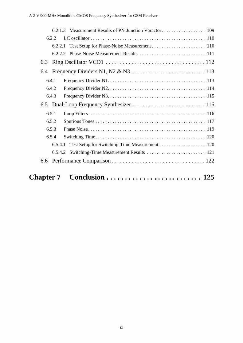
2.1 Blocking Profile of GSM 900
In receiver band for GSM specification, which is 25 MHz wide, ranges from 935 to
960 MHz. It consists of 124 channels with channel bandwidth of 200 kHz. The center
frequencies of the channels (fchannel) are
(2.1)
whereN = 1, 2,..., 124.
Figure 2.1 shows the profile of the blocking and adjacent signals of GSM 900 [5]. The
minimum power of the desired RF signals can be as low as -102 dBm. Around the desired
channel, the adjacent-channel power at±200-kHz,±400-kHz and±600-kHz frequency offset
are 9 dB, 41 dB and 49 dB above the desired signal respectively. Beside the adjacent channels,
blocking signals exist at±600-kHz,±1.6-MHz and±3-MHz frequency offset with power of -43
dBm, -33 dBm and -23 dBm respectively. Outside the receiver band, the power of blocking
signals can be up to 0 dBm. If the LNA and the RF filters provide sufficient filtering of
out-of-band blocking signals, the effect of these blocking signals can be ignored.
f channel 935.2 0.2 N 1–( ) MHz⋅+=
2-V 900-MHz Monolithic CMOS Frequency Synthesizer for GSM Receiver
7
2.2 Design-Specification Derivation
For GSM receiver front-end application, frequency synthesizer can be characterized by
the phase noise, spurious tones and switching speed. Their specifications are discussed in this
chapter.
2.2.1 Phase Noise
Phase noise is characterized in the frequency domain. For an oscillator operating at
frequencyωo, the VCO output can be expressed as
(2.2)
whereA is the output amplitude, andθ(t) is the output phase which is time-varying due to the
existence of phase noise. Due to random phase fluctuations, the VCO-output spectrum has
side-band noise close to the oscillation frequency as shown in Figure 2.3.
Figure 2.1 Blocking profile for GSM 900.
Vo A ωot θ t( )+( )sin⋅=
2-V 900-MHz Monolithic CMOS Frequency Synthesizer for GSM Receiver
8
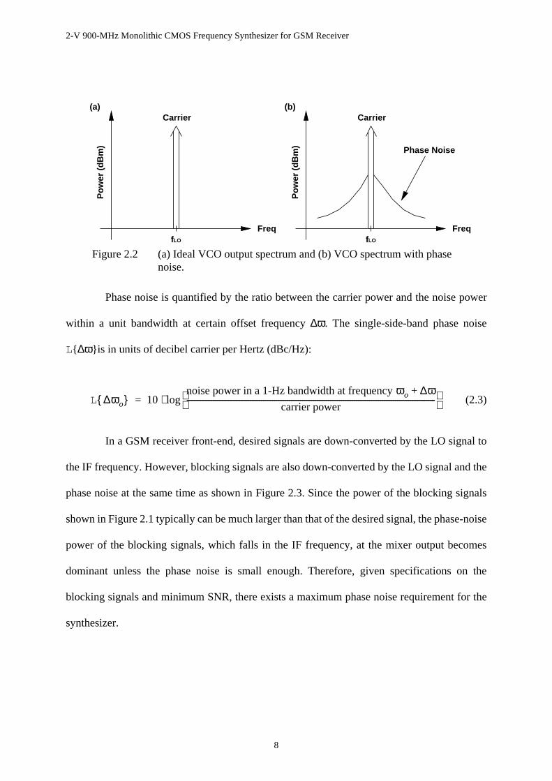
Phase noise is quantified by the ratio between the carrier power and the noise power
within a unit bandwidth at certain offset frequency∆ω. The single-side-band phase noise
L ∆ωis in units of decibel carrier per Hertz (dBc/Hz):
(2.3)
In a GSM receiver front-end, desired signals are down-converted by the LO signal to
the IF frequency. However, blocking signals are also down-converted by the LO signal and the
phase noise at the same time as shown in Figure 2.3. Since the power of the blocking signals
shown in Figure 2.1 typically can be much larger than that of the desired signal, the phase-noise
power of the blocking signals, which falls in the IF frequency, at the mixer output becomes
dominant unless the phase noise is small enough. Therefore, given specifications on the
blocking signals and minimum SNR, there exists a maximum phase noise requirement for the
synthesizer.
fLO
Phase Noise
Carrier
Po
wer
(d
Bm
)
FreqfLO
Carrier
Po
wer
(d
Bm
)
Freq
(a) (b)
Figure 2.2 (a) Ideal VCO output spectrum and (b) VCO spectrum with phasenoise.
L ∆ωo 10noise power in a 1-Hz bandwidth at frequencyωo ∆ω+
carrier power--------------------------------------------------------------------------------------------------------------------------------------
log⋅=
2-V 900-MHz Monolithic CMOS Frequency Synthesizer for GSM Receiver
9
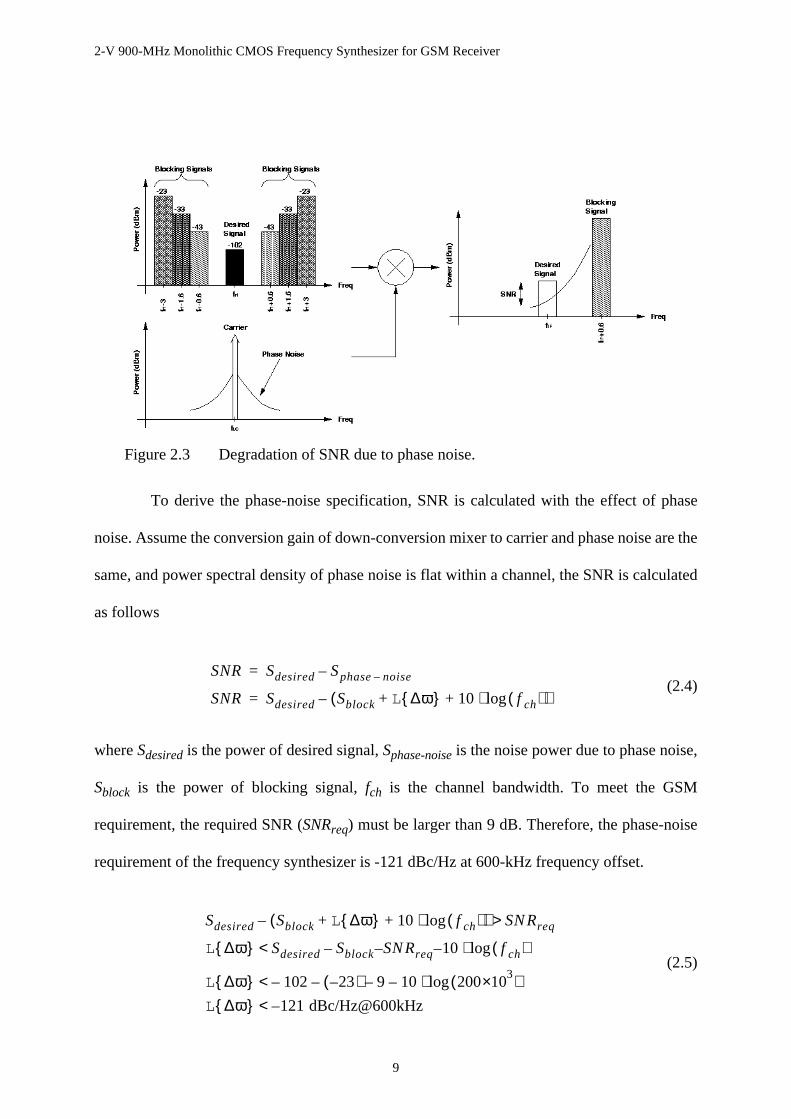
To derive the phase-noise specification, SNR is calculated with the effect of phase
noise. Assume the conversion gain of down-conversion mixer to carrier and phase noise are the
same, and power spectral density of phase noise is flat within a channel, the SNR is calculated
as follows
(2.4)
whereSdesired is the power of desired signal,Sphase-noise is the noise power due to phase noise,
Sblock is the power of blocking signal,fch is the channel bandwidth. To meet the GSM
requirement, the required SNR (SNRreq) must be larger than 9 dB. Therefore, the phase-noise
requirement of the frequency synthesizer is -121 dBc/Hz at 600-kHz frequency offset.
(2.5)
Figure 2.3 Degradation of SNR due to phase noise.
SNR Sdesired Sphase noise––=
SNR Sdesired Sblock L ∆ω 10 f ch( )log⋅+ +( )–=
Sdesired Sblock L ∆ω 10 f ch( )log⋅+ +( ) SNRreq>–
L ∆ω Sdesired Sblock SNRreq– 10– f ch( )log⋅–<
L ∆ω 102– 23–( )– 9– 10 2003×10( )log⋅–<
L ∆ω 121 dBc/Hz@600kHz–<
2-V 900-MHz Monolithic CMOS Frequency Synthesizer for GSM Receiver
10
The same method shows the phase noise specification at offset frequencies of 1.6 MHz
and 3 MHz are -131 and -141 dBc/Hz respectively. Assuming a dependence of 20 dB per decade
on offset frequency [3], the most critical phase-noise requirement which is referred to 600-kHz
frequency offset is actually at the 3-MHz frequency offset (-127 dBc/Hz@600kHz). However,
the state of the art on-chip voltage-controlled oscillator still cannot meet phase-noise
specification at 3-MHz offset [6]. Therefore, this synthesizer is designed to satisfy the
phase-noise requirement only at 600-kHz frequency offset.
2.2.2 Spurious-Tone Specification
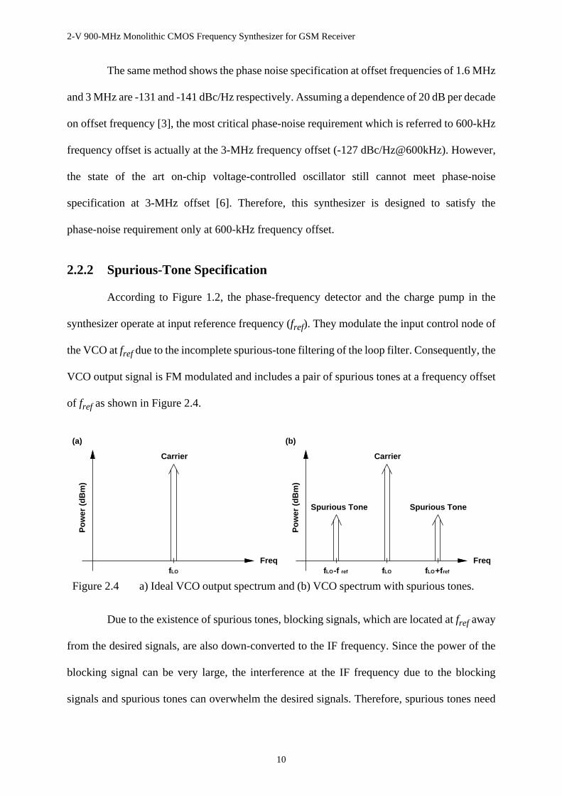
According to Figure 1.2, the phase-frequency detector and the charge pump in the
synthesizer operate at input reference frequency (fref). They modulate the input control node of
the VCO atfref due to the incomplete spurious-tone filtering of the loop filter. Consequently, the
VCO output signal is FM modulated and includes a pair of spurious tones at a frequency offset
of fref as shown in Figure 2.4.
Due to the existence of spurious tones, blocking signals, which are located atfref away
from the desired signals, are also down-converted to the IF frequency. Since the power of the
blocking signal can be very large, the interference at the IF frequency due to the blocking
signals and spurious tones can overwhelm the desired signals. Therefore, spurious tones need
fLO
Carrier
-f reffLO
Spurious Tone
fLO+fref
Spurious Tone
Pow
er (
dBm
)
FreqfLO
Carrier
Pow
er (
dBm
)
Freq
(a) (b)
Figure 2.4 a) Ideal VCO output spectrum and (b) VCO spectrum with spurious tones.
2-V 900-MHz Monolithic CMOS Frequency Synthesizer for GSM Receiver
11
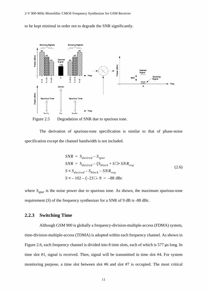
to be kept minimal in order not to degrade the SNR significantly.
The derivation of spurious-tone specification is similar to that of phase-noise
specification except the channel bandwidth is not included.
(2.6)
whereSspur is the noise power due to spurious tone. As shown, the maximum spurious-tone
requirement (S) of the frequency synthesizer for a SNR of 9 dB is -88 dBc.
2.2.3 Switching Time
Although GSM 900 is globally a frequency-division-multiple-access (FDMA) system,
time-division-multiple-access (TDMA) is adopted within each frequency channel. As shown in
Figure 2.6, each frequency channel is divided into 8 time slots, each of which is 577µs long. In
time slot #1, signal is received. Then, signal will be transmitted in time slot #4. For system
monitoring purpose, a time slot between slot #6 and slot #7 is occupied. The most critical
Figure 2.5 Degradation of SNR due to spurious tone.
SNR Sdesired Sspur–=
SNR Sdesired Sblock S+( ) SNRreq>–=
S Sdesired Sblock– SNRreq–<
S 102– 23–( )– 9–< 88 dBc–=
2-V 900-MHz Monolithic CMOS Frequency Synthesizer for GSM Receiver
12
switching time is from transmission period (slot #4) to system-monitoring period (between slot
#6 and slot #7). Therefore, the settling-time requirement of the frequency synthesizer is 1.5 time
slots which is equal to 870µs. As a consequent, to meet the specification with a frequency step
of 100 MHz and frequency accuracy of 100 Hz, minimum loop bandwidth of a first-order loop
is 3.1 kHz.
Table 2.1 summaries the design specifications of the frequency synthesizer for GSM
receiver application. The requirement derivation of phase noise, spurious tones and switching
time are explained in the previous sections. The supply voltage is reduced to 2 V for better
digital-circuit compatibility and better reliability for device scaling down to deep-submicron
process. The power consumption is designed not to be larger than what has been reported [3].
The chip area is limited to be less than 2× 2 mm2 which is the minimum chip size of the process.
577 µs
RX on:
TX on:
R1 R2 R3 R4 R5 R6 R7 R8 R1 R2R8
T1 T2 T3 T4 T5 T6 T7T8T7T6T5
Receive
Transmit
Sys. Monitor Receive
Figure 2.6 GSM 900 receive (RX) and transmit (TX) time slots.
Parameters Specification
Phase Noise < -121 dBc/Hz@600kHz
Spurious Tones < -88 dBc
Settling Time < 870µs
Supply Voltage 2 V
Power < 50 mW
Area < 2 × 2 mm2
Process HP 0.5-µm CMOS
Table 2.1 Design specifications of the frequency synthesizer.

2-V 900-MHz Monolithic CMOS Frequency Synthesizer for GSM Receiver
13
The synthesizer is implemented by HP 0.5-µm CMOS process which provides linear capacitor
and silicide-blocked polysilicon for the implementation of the on-chip loop filters.

2-V 900-MHz Monolithic CMOS Frequency Synthesizer for GSM Receiver
14
Chapter 3
Dual-Loop Frequency Synthesizer
3.1 Architecture of Dual-Loop Design
To reduce the chip area and switching time, a higher input-reference frequency is
desired. Moreover, to improve frequency-divider complexity, a lower frequency-division ratio
is desirable for the programmable divider. Therefore, a dual-loop frequency synthesizer is
considered [7]. As shown in Figure 3.1, the proposed dual-loop synthesizer to be designed and
presented in this thesis consists of two crystal oscillators and two phase-locked loops connected
in series. The low-frequency loop (LFL), which is on the left hand side, has a programmable
frequency dividerN1 for channel selection. The high-frequency loop (HFL), which is on the
fref2 = 205 MHz
fo = 865.2 ~ 889.8 MHz
2 = 32N
fin2 = 11.3 ~ 17.45 MHz
N = 2261
~ 349
fref1 /f in1 = 1.6 MHz
Mixer3 = 4
VCO2
361.6 ~ 558.4 MHz
VCO1
N
CP1& LF1
PFD1
& LF2CP2
PFD2
High-Frequency Loop (HFL)
Low
-Fre
quen
cy L
oop
(LF
L)
Figure 3.1 Block diagrams of the proposed dual-loop frequency synthesizer.
2-V 900-MHz Monolithic CMOS Frequency Synthesizer for GSM Receiver
15
right hand side, has a down-conversion mixer in its feedback path to provide a constant
frequency offset at the output. In between LFL and HFL, a fixed frequency dividerN2 is
included for phase-noise and spurious-tone suppression of the low-frequency loop
When both phase-locked loops lock, the output frequency (fo) of synthesizer is
expressed as follows
(3.1)
wherefref1 andfref2 are reference frequencies of two crystal oscillators,N1 is the division ratio
of the programmable frequency divider,N2 andN3 are division ratios of the fixed frequency
dividers. The output frequency can be expressed in terms of constant frequency offset (foffset)
and channel spacing (fch) as follows.
(3.2)
By mapping the terms in (3.1) and (3.2), the offset frequencyfoffset and the channel spacingfch
can then be expressed in terms of the PLL parameters.
(3.3)
(3.4)
From (3.3), the offset frequency is designed at 820 MHz so that the frequency-division ratios of
N2 andN3 are multiples of 2 which makes the implementation of the frequency dividers much
easier. From (3.4), it can be found that the input reference frequency of the low-frequency loop
(fref1) is increased by 8 times which is limited by the frequency range of the VCO in the
f o N3 f ref 2 N1
N3
N2------
f ref 1+ 865.2 ~ 889.8 MHz= =
f o f offset N1 f ch+=
f offset N3 f ref 2 4 205× 820 MHz= = =
f ch
N3
N2------
f ref 1=
f ref 1⇒N2
N3------
f ch324------
200k⋅ 1.6 MHz= = =
2-V 900-MHz Monolithic CMOS Frequency Synthesizer for GSM Receiver
16
low-frequency loop as discussed in Section 3.3.1. The increase in reference frequency relaxes
the loop-bandwidth requirement.
3.2 Advantages of the Dual-Loop Design
3.2.1 Smaller Chip Area and Faster Switching Time
Due to the dual-loop architecture, input frequencies of both low-frequency and
high-frequency loops are scaled up to and
respectively. Therefore, the loop bandwidths of both PLLs can be increased to achieve smaller
chip area and faster settling time.
3.2.2 Simpler Programmable-Frequency-Divider Design
As a down-conversion mixer is included in the feedback path of the high-frequency
loop, a constant frequency offset (foffset) is created by the second reference frequency (fref2).
Therefore, the frequency-division ratio of the programmable dividerN1 can be reduced from
4236 ~ 4449 to 226 ~ 349. The reduced division ratio simplifies the design and reduces
phase-noise contribution from input reference.
3.3 Potential Disadvantages of the Dual-Loop Design
3.3.1 Requirement of a Larger VCO-Tuning Range
Although the low-frequency-loop input frequency is scaled up from 200 kHz to 1.6
MHz, the frequency-tuning range of the VCO1 in the low-frequency loop is scaled up from 25
MHz to 200 MHz at the same time which corresponds to an increase in the tuning range from
4% to 33%. Because of the large frequency-tuning range requirement, LC-oscillators cannot be
adopted and only ring oscillators can be used. It is very challenging to design a ring oscillator
with low phase noise (-103 dBc/Hz@600kHz), high frequency (600 MHz), and wide
f in1 1.6 MHz= f in2 11.3 ~ 17.45 MHz=
2-V 900-MHz Monolithic CMOS Frequency Synthesizer for GSM Receiver
17
tuning-range (50%).
3.3.2 Additional Chip area and Phase Noise
Since the dual-loop design consists of two PLLs, the additional PLL may require extra
chip area and contribute extra phase noise and spurious tones. However, as the combination of
frequency dividersN2 andN3 provides 18-dB suppression of phase-noise and spurious-tone
contributed by the low-frequency loop, the design specification of the low-frequency loop is
relaxed. Therefore, phase-noise contribution from the LFL is suppressed and a smaller loop
filter can be adopted to achieve the same spurious-tone requirement. Phase-noise and
spurious-tone performance of the whole frequency synthesizer is dominated by that of the
high-frequency loop.
3.3.3 Long Switching Time
As the dual-loop design has two PLLs in cascade configuration, the switching time of
the dual-loop design is slower than a single-loop design. However, the switching-time
requirement of the GSM receiver is 865µs which is not very fast. Therefore, if both
low-frequency and high-frequency loops have loop bandwidth larger than 6 kHz, the
switching-time requirement can be satisfied.
3.3.4 Image-Output Frequency
Due to the existence of the down-conversion mixer in the feedback path of the
high-frequency loop, the proposed synthesizer can also be locked at the image-output frequency
fo-image
(3.5)
Fortunately, the VCO of the high-frequency loop is implemented by a LC oscillator which does
f o eimag– N3 f ref 2 N1
N3
N2------
f ref 1– 750.2 ~ 774.8 MHz= =
2-V 900-MHz Monolithic CMOS Frequency Synthesizer for GSM Receiver
18
not operate in the image-output frequency range. Therefore, image-rejection mixer is not
required for the implementation of the down-conversion mixer.
3.3.5 Additional Design Effort
As the proposed dual-loop frequency synthesizer consists of two VCOs, two loop
filters, three frequency dividers, two PFDs, two charge pumps and a down-conversion mixer,
more design effort is required.

2-V 900-MHz Monolithic CMOS Frequency Synthesizer for GSM Receiver
19
Chapter 4
Circuit Implementation
4.1 Introduction
In this chapter, circuit implementation of all the building blocks of the dual-loop
frequency synthesizer is discussed. Analysis, design and simulation results of the circuit are
presented for each building block. In the first part of this chapter, building blocks of the
high-frequency loop, including the voltage-controlled oscillator VCO2, the frequency dividers
N2 and N3, and the down-conversion mixer are analysed and discussed. Then the building
blocks of the low-frequency loop, including the voltage-controlled oscillator VCO1, and the
programmable frequencyN1 are described. After that, the blocks common in both PLLs, such
as phase-frequency detectors PFDs, charge pumps CPs, and loop filters LFs are discussed. At
the end, the simulation and estimated results of the dual-loop frequency synthesizer will be
presented.
4.2 Voltage-Controlled Oscillator VCO2
4.2.1 Design Requirement
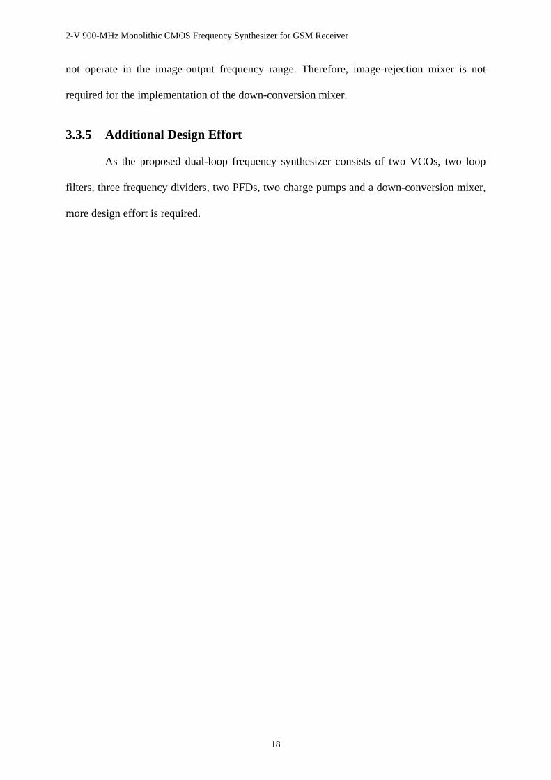
Voltage-controlled oscillator VCO2, which generates output frequency, locates in the
high-frequency loop as shown in Figure 4.1. The design requirement of VCO2 is as follows
2-V 900-MHz Monolithic CMOS Frequency Synthesizer for GSM Receiver
20
• It should cover the output frequencies from 865.2 to 889.8 MHz.
• It should satisfy the phase-noise performance -121 dBc/Hz@600kHz with
minimum power consumption.
• It should generate output signals with single-ended amplitude larger than 0.5 V to
drive the fixed frequency dividerN3.
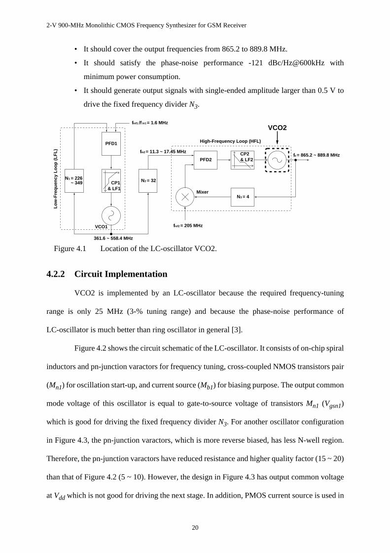
4.2.2 Circuit Implementation
VCO2 is implemented by an LC-oscillator because the required frequency-tuning
range is only 25 MHz (3-% tuning range) and because the phase-noise performance of
LC-oscillator is much better than ring oscillator in general [3].
Figure 4.2 shows the circuit schematic of the LC-oscillator. It consists of on-chip spiral
inductors and pn-junction varactors for frequency tuning, cross-coupled NMOS transistors pair
(Mn1) for oscillation start-up, and current source (Mb1) for biasing purpose. The output common
mode voltage of this oscillator is equal to gate-to-source voltage of transistorsMn1 (Vgsn1)
which is good for driving the fixed frequency dividerN3. For another oscillator configuration
in Figure 4.3, the pn-junction varactors, which is more reverse biased, has less N-well region.
Therefore, the pn-junction varactors have reduced resistance and higher quality factor (15 ~ 20)
than that of Figure 4.2 (5 ~ 10). However, the design in Figure 4.3 has output common voltage
atVdd which is not good for driving the next stage. In addition, PMOS current source is used in
fref2 = 205 MHz
fo = 865.2 ~ 889.8 MHz
2 = 32N
f = 11.3 ~ 17.45 MHz
N = 2261
~ 349
fref1
in2
in1 = 1.6 MHz/f
Mixer3 = 4
High-Frequency Loop (HFL)
361.6 ~ 558.4 MHz
VCO1
Low
-Fre
quen
cy L
oop
(LF
L)
VCO2
N
CP1& LF1
PFD1
& LF2CP2
PFD2
Figure 4.1 Location of the LC-oscillator VCO2.

2-V 900-MHz Monolithic CMOS Frequency Synthesizer for GSM Receiver
21
the design of Figure 4.2 to reduce flicker-noise component. Therefore, the oscillator
configuration in Figure 4.2 is adopted.
4.2.3 LC-Oscillator Analysis
To analyse the power consumption, oscillating frequency and phase noise of the
Mn1 Mn1
Mb1Mb1
CpCp Vc
Vdd
Ibiaso+V o-V
Figure 4.2 Circuit implementation of the LC-oscillator VCO2.
Figure 4.3 Another possible implementation of the LC-oscillator.
Vdd
Mn1 Mn1
CpCp Vco+V o-V
Mb1 Mb1
Ibias

2-V 900-MHz Monolithic CMOS Frequency Synthesizer for GSM Receiver
22
LC-oscillator, the linear circuit model of the LC tank in Figure 4.4 is used. The model consists
of an on-chip inductor, pn-junction varactor and the parasitics of transistorMn1.
The single-ended output admittance of the LC-tankYLC ω is expressed as follows
(4.1)
whereL, RL, Cs, Rs are inductance, series resistance, substrate capacitance, series substrate
resistance of the on-chip spiral inductor respectively,Cc andRc are capacitance and series
resistance of the pn-junction of varactor respectively,Cp andRp are the device parasitics of
transistorMn1.
4.2.3.1 Power Consumption
The minimum transconductanceGm_min of the transistorsMn1, which starts the
oscillation, should be larger or equal to the real part of LC-tank admittanceReal[YLC ω] [8].
RL
Cs
Rs
Cc
Rc
Cp Rp
L
Device ParasiticsVaractorSpiral Inductor
Figure 4.4 Linear circuit model of the LC tank.
YLC ω RL
RL2 ωL( )2
+----------------------------
Rs ωCs( )2
1 ωRsCs( )2+
--------------------------------- 1Rp------
Rc ωCc( )2
1 ωRc2Cc
2( )+-------------------------------+ + +
=
jω L–
RL2 ωL( )2
+----------------------------
Cs
1 ωRsCs( )2+
--------------------------------- Cp
Cc
1 ωRc2Cc
2( )+-------------------------------+ + +
⋅+
2-V 900-MHz Monolithic CMOS Frequency Synthesizer for GSM Receiver
23
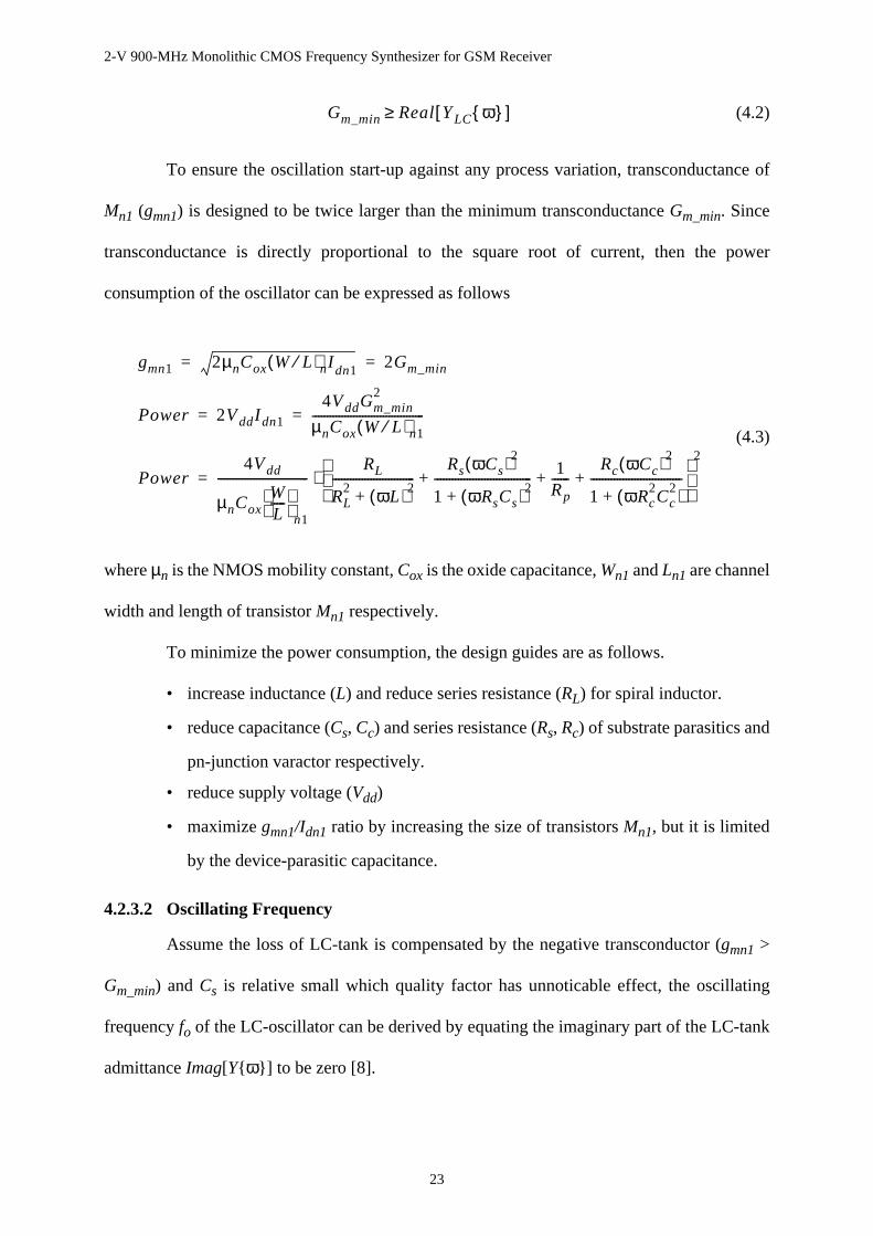
(4.2)
To ensure the oscillation start-up against any process variation, transconductance of
Mn1 (gmn1) is designed to be twice larger than the minimum transconductanceGm_min. Since
transconductance is directly proportional to the square root of current, then the power
consumption of the oscillator can be expressed as follows
(4.3)
whereµn is the NMOS mobility constant,Cox is the oxide capacitance,Wn1 andLn1 are channel
width and length of transistorMn1 respectively.
To minimize the power consumption, the design guides are as follows.
• increase inductance (L) and reduce series resistance (RL) for spiral inductor.
• reduce capacitance (Cs, Cc) and series resistance (Rs, Rc) of substrate parasitics and
pn-junction varactor respectively.
• reduce supply voltage (Vdd)
• maximizegmn1/Idn1 ratio by increasing the size of transistorsMn1, but it is limited
by the device-parasitic capacitance.
4.2.3.2 Oscillating Frequency
Assume the loss of LC-tank is compensated by the negative transconductor (gmn1 >
Gm_min) andCs is relative small which quality factor has unnoticable effect, the oscillating
frequencyfo of the LC-oscillator can be derived by equating the imaginary part of the LC-tank
admittanceImag[Y ω] to be zero [8].
Gm_min Real YLC ω [ ]≥
gmn1 2µnCox W L⁄( )nI dn1 2Gm_min= =
Power 2VddI dn1
4VddGm_min2
µnCox W L⁄( )n1--------------------------------------= =
Power4Vdd
µnCoxWL-----
n1
-------------------------------RL
RL2 ωL( )2
+----------------------------
Rs ωCs( )2
1 ωRsCs( )2+
--------------------------------- 1Rp------
Rc ωCc( )2
1 ωRc2Cc
2( )+-------------------------------+ + +
2
⋅=
2-V 900-MHz Monolithic CMOS Frequency Synthesizer for GSM Receiver
24
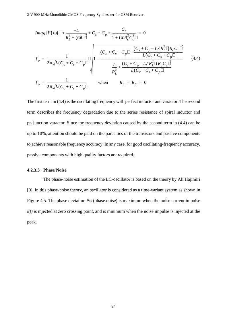
(4.4)
The first term in (4.4) is the oscillating frequency with perfect inductor and varactor. The second
term describes the frequency degradation due to the series resistance of spiral inductor and
pn-junction varactor. Since the frequency deviation caused by the second term in (4.4) can be
up to 10%, attention should be paid on the parasitics of the transistors and passive components
to achieve reasonable frequency accuracy. In any case, for good oscillating-frequency accuracy,
passive components with high quality factors are required.
4.2.3.3 Phase Noise
The phase-noise estimation of the LC-oscillator is based on the theory by Ali Hajimiri
[9]. In this phase-noise theory, an oscillator is considered as a time-variant system as shown in
Figure 4.5. The phase deviation∆φ (phase noise) is maximum when the noise current impulse
i(t) is injected at zero crossing point, and is minimum when the noise impulse is injected at the
peak.
Imag Y ω [ ] L–
RL2 ωL( )2
+---------------------------- Cs Cp
Cc
1 ωRc2Cc
2( )+-------------------------------+ + +≈ 0=
f o1
2π L Cc Cs Cp+ +( )---------------------------------------------------- 1
Cc Cs Cp+ +( )Cs Cp L RL
2⁄–+( ) RcCc( )2
L Cc Cs Cp+ +( )----------------------------------------------------------------+
L
RL2
------Cs Cp L RL
2⁄–+( ) RcCc( )2
L Cc Cs Cp+ +( )----------------------------------------------------------------+
------------------------------------------------------------------------------------------------------------–⋅=
f o1
2π L Cc Cs Cp+ +( )----------------------------------------------------= when RL RC 0= =
2-V 900-MHz Monolithic CMOS Frequency Synthesizer for GSM Receiver
25
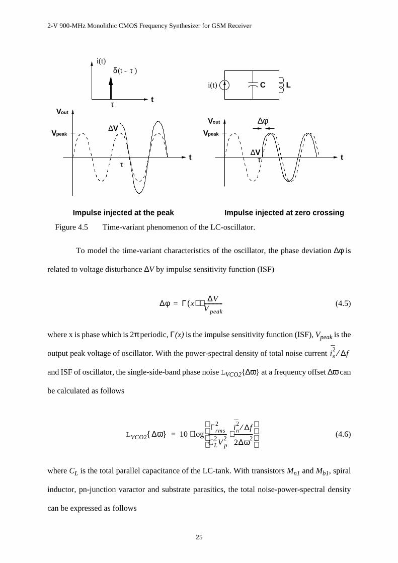
To model the time-variant characteristics of the oscillator, the phase deviation∆φ is
related to voltage disturbance∆V by impulse sensitivity function (ISF)
(4.5)
where x is phase which is 2π periodic,Γ(x) is the impulse sensitivity function (ISF),Vpeak is the
output peak voltage of oscillator. With the power-spectral density of total noise current
and ISF of oscillator, the single-side-band phase noiseLVCO2 ∆ω at a frequency offset∆ω can
be calculated as follows
(4.6)
whereCL is the total parallel capacitance of the LC-tank. With transistorsMn1 andMb1, spiral
inductor, pn-junction varactor and substrate parasitics, the total noise-power-spectral density
can be expressed as follows
VpeakVpeak∆V
outV
tτ
∆V
outV
tτ
i(t) C L
δ (t - τ )
∆φ
Impulse injected at the peak Impulse injected at zero crossing
i(t)
τ t
Figure 4.5 Time-variant phenomenon of the LC-oscillator.
∆φ Γ x( ) ∆VVpeak--------------⋅=
in2 ∆f⁄
LVCO2 ∆ω 10Γrms
2
CL2Vp
2--------------
in2 ∆f⁄
2∆ω2--------------⋅
log⋅=

2-V 900-MHz Monolithic CMOS Frequency Synthesizer for GSM Receiver
26
(4.7)
wherek is Boltzmann’s constant,T is absolute temperature,QL, QS andQC are quality factors
of inductor, substrate parasitics and varactor respectively. The first coefficient “2” in (4.7)
accounts for the double noise sources of the differential design.
To minimize phase noise, the design guidelines are as follows
• do not over-compensate the LC-tank too much (gmn1 > 2Gm_min) to reduce the
requiredgmn1.
• reducegmb1/Idb1 ratio by increasing the size of transistorsMb1.
• minimize series resistanceRL, RS, RC and maximize the quality factorQL, QS, QC
for spiral inductor, substrate parasitics and pn-junction varactor respectively.
• maximize output amplitudeVp by increasing the bias current.
To achieve a low power, good frequency accuracy and low phase noise for the
oscillator, passive components, such as inductors and varactors, with good quality factors are
required in general. The design of on-chip spiral inductors and pn-junction varactors will be
discussed in the next two sections.
4.2.4 Design of the On-Chip Spiral Inductor
Since most standard CMOS process is for digital circuit application, metal layers are
less than 1µm and epitaxial substrate is used for latchup consideration. Due to the metal
resistance, skin effect and substrate loss in epitaxial substrate, quality factor of on-chip spiral
inductor is difficult to be larger than three. This section summaries the design guidelines of the
on-chip spiral-inductor design.
4.2.4.1 Circular Spiral Inductor
On-chip spiral inductor can be built in different geometries like square, octagon and
in2
∆f------ 2 4kT 3 gmn1⋅ 3
gmb1
2----------- 1
RL 1 QL2
+( )---------------------------- 1
Rs 1 QS2
+( )--------------------------- 1
Rc 1 QC2
+( )----------------------------+ + +⋅+
⋅ ⋅=
QL ωL RL⁄= QS 1 ωRSCS⁄= QC 1 ωRCCC⁄=
2-V 900-MHz Monolithic CMOS Frequency Synthesizer for GSM Receiver
27
circle. Compared to a circular inductor, a square spiral inductor has larger inductance-to-area
ratio but contributes more series resistance at the coil corners. Therefore, a circular spiral
inductor is adopted to eliminate the corner resistance and thus enhance the quality-factor
optimization.
4.2.4.2 Minimum Metal Spacing
By adopting minimum metal spacing, the magnetic coupling between adjacent metal
lines is maximized [10]. The additional inter-winding capacitance from tighter coupling of the
electric field between adjacent conductors reduces the self-resonant frequency to around 3 GHz,
but it has little impact on performance in 900-MHz operation. Therefore, minimum metal
spacing maximizes the quality factor and reduces the chip area for a given inductor layout.
4.2.4.3 Limited Metal Width
At high frequency operation, skin effect causes a non-uniform current flow in metal
lines, and increases the series resistance of the spiral inductor. From the analysis by Jan
Craninckx [11], two inductors with metal width of 15µm and 30µm, while other parameters
are the same, are simulated. The simulation results at 2 GHz show the series resistance with
metal width 30µm is only 30% lower than the other one. Moreover, widening the metal lines
of inductors with a fixed area will result in a smaller inductance value. To keep the inductance
value constant, inductor area must be increased and result in larger substrate capacitance. The
increase in capacitance causes lower self-resonant frequency and more substrate loss.
Therefore, very wide metal (> 30µm) is not desirable for inductor optimization.
4.2.4.4 Hollow-Spiral Inductor
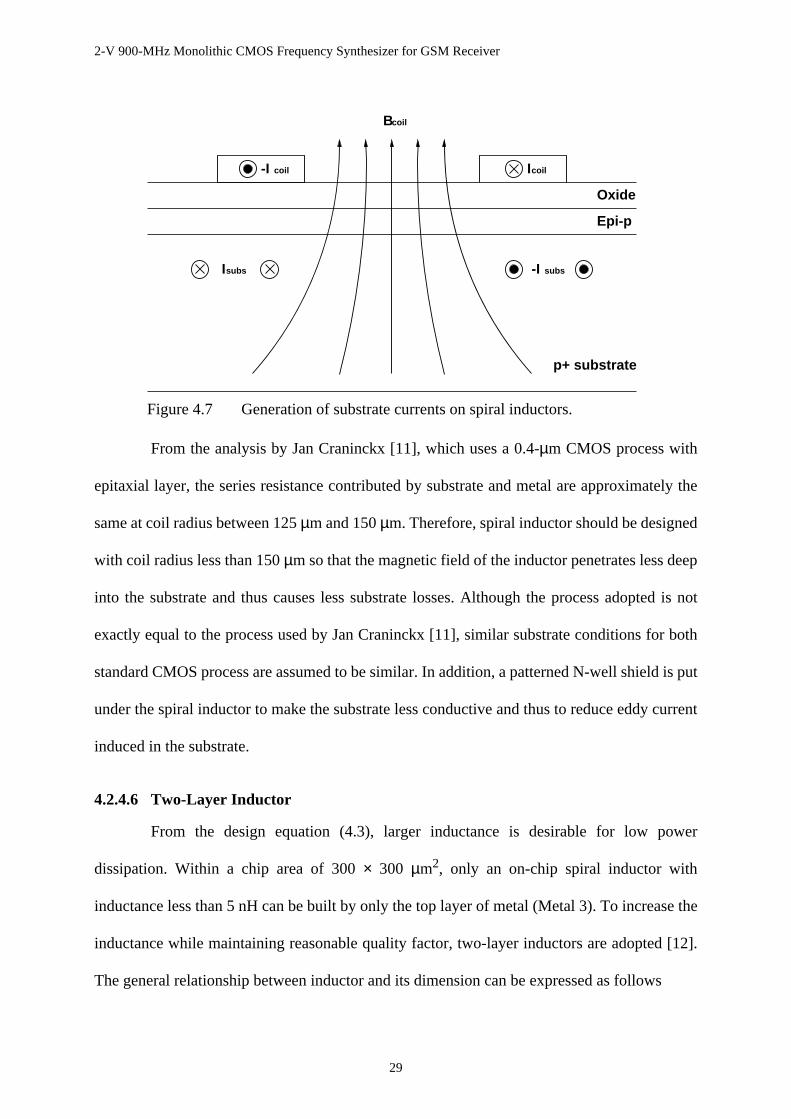
To maximize the inductance per unit area, it seems that inductor coil should fill up the
whole area. However, quality factor of spiral inductor is degraded by eddy current generated in
the inner coils as shown in Figure 4.6. The inductor has a currentIcoil which induces a magnetic

2-V 900-MHz Monolithic CMOS Frequency Synthesizer for GSM Receiver
28
field Bcoil with maximum intensity at the center of the inductor. According to the theory by
Faraday-Lenz, the magnetic fieldBcoil generates a circular eddy currentIeddy. Such generated
eddy current degrades the quality factor of spiral inductor in two folds. First, the eddy current
induces a magnetic fieldBeddy, which opposes the original magnetic field, so inductance value
decreases. Second, the eddy current causes a non-uniform current flow in the inner coil of
inductor, so current is pushed inside the metal line and series resistance is increased [11].
Therefore, to eliminate the quality-factor degradation of spiral inductor, hollow spiral
inductor with 50-% inner-hole size is adopted in this design [11].
4.2.4.5 Limited Inductor Area
As epi-wafer is used in this technology, currents induced by the magnetic field of the
inductor are free to flow, which causes extra quality-factor degradation of inductors as shown
in Figure 4.7. According to the theory by Faraday-Lenz, electrical current is magnetically
induced in substrate. The induced substrate current flows in a direction opposite to the current
in the inductor and thus causes quality-factor degradation.
Icoil
Icoil
Bcoil
Beddy
Ieddy
Magnetic field flows out of page Magnetic field flows into the page
Outer Coil
Inner Coil
Figure 4.6 Generation of eddy currents in spiral inductor.
2-V 900-MHz Monolithic CMOS Frequency Synthesizer for GSM Receiver
29
From the analysis by Jan Craninckx [11], which uses a 0.4-µm CMOS process with
epitaxial layer, the series resistance contributed by substrate and metal are approximately the
same at coil radius between 125µm and 150µm. Therefore, spiral inductor should be designed
with coil radius less than 150µm so that the magnetic field of the inductor penetrates less deep
into the substrate and thus causes less substrate losses. Although the process adopted is not
exactly equal to the process used by Jan Craninckx [11], similar substrate conditions for both
standard CMOS process are assumed to be similar. In addition, a patterned N-well shield is put
under the spiral inductor to make the substrate less conductive and thus to reduce eddy current
induced in the substrate.
4.2.4.6 Two-Layer Inductor
From the design equation (4.3), larger inductance is desirable for low power
dissipation. Within a chip area of 300× 300 µm2, only an on-chip spiral inductor with
inductance less than 5 nH can be built by only the top layer of metal (Metal 3). To increase the
inductance while maintaining reasonable quality factor, two-layer inductors are adopted [12].
The general relationship between inductor and its dimension can be expressed as follows
Icoil
-I subsIsubs
-I coil
Bcoil
Oxide
Epi-p
p+ substrate
Figure 4.7 Generation of substrate currents on spiral inductors.
2-V 900-MHz Monolithic CMOS Frequency Synthesizer for GSM Receiver
30
(4.8)
where N is number of turn,A is cross-section area, andl is the length of solenoids. By
connecting two layers of spiral inductors in series, inductance can increased by 4 times with the
same inductor area since inductance is proportional toN2. Moreover, series resistance is only
proportional toN, quality factor of inductor can also be improved simultaneously. However, the
quality-factor improvement of two-layer inductors is smaller than twice since the lower layer of
metal has higher sheet resistance and larger substrate capacitance.
4.2.4.7 Inductor Simulation and Modelling
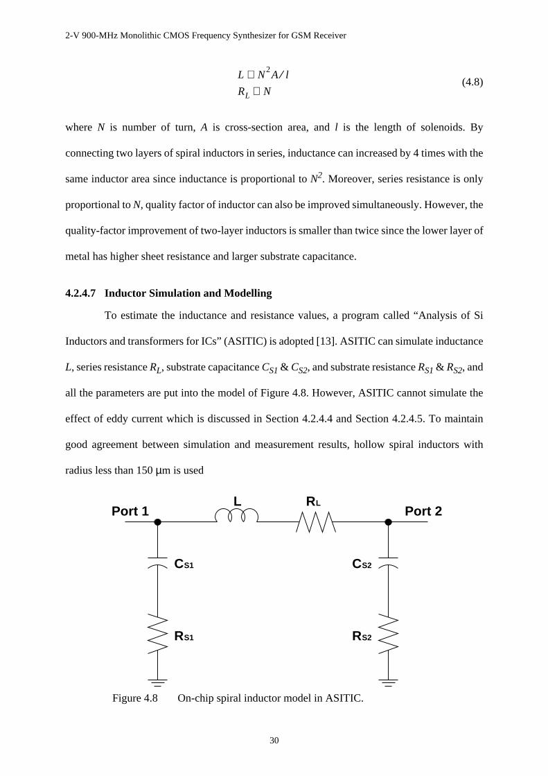
To estimate the inductance and resistance values, a program called “Analysis of Si
Inductors and transformers for ICs” (ASITIC) is adopted [13]. ASITIC can simulate inductance
L, series resistanceRL, substrate capacitanceCS1 & CS2, and substrate resistanceRS1 & RS2, and
all the parameters are put into the model of Figure 4.8. However, ASITIC cannot simulate the
effect of eddy current which is discussed in Section 4.2.4.4 and Section 4.2.4.5. To maintain
good agreement between simulation and measurement results, hollow spiral inductors with
radius less than 150µm is used
L N2A l⁄∝
RL N∝
LR
CS1
RS1
S2C
S2R
Port 1L
Port 2
Figure 4.8 On-chip spiral inductor model in ASITIC.
2-V 900-MHz Monolithic CMOS Frequency Synthesizer for GSM Receiver
31
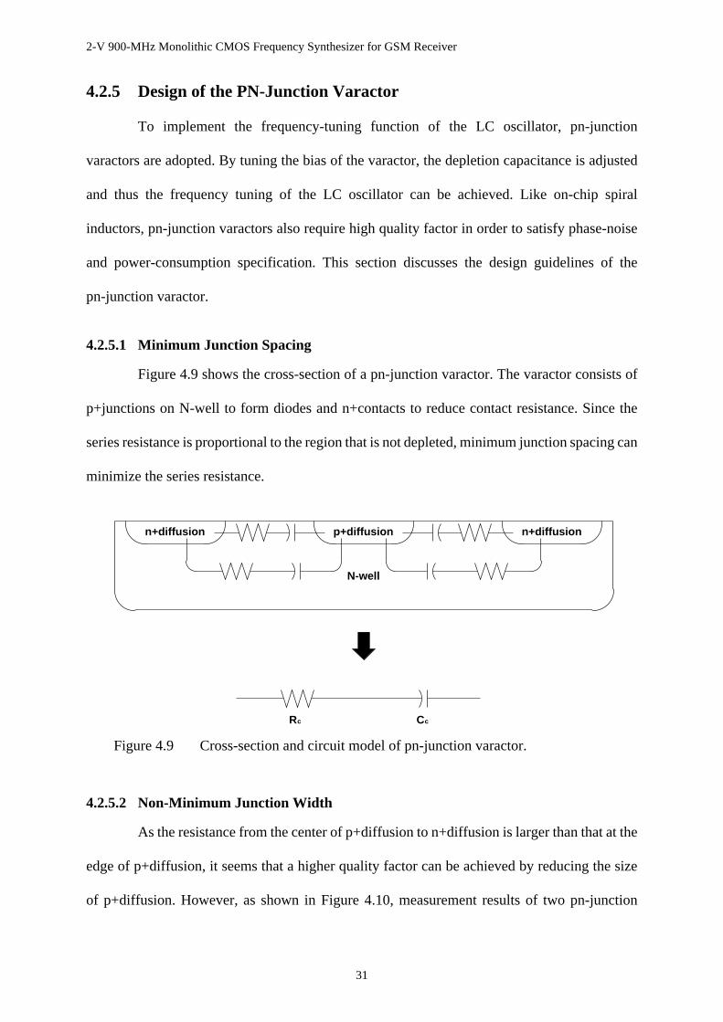
4.2.5 Design of the PN-Junction Varactor
To implement the frequency-tuning function of the LC oscillator, pn-junction
varactors are adopted. By tuning the bias of the varactor, the depletion capacitance is adjusted
and thus the frequency tuning of the LC oscillator can be achieved. Like on-chip spiral
inductors, pn-junction varactors also require high quality factor in order to satisfy phase-noise
and power-consumption specification. This section discusses the design guidelines of the
pn-junction varactor.
4.2.5.1 Minimum Junction Spacing
Figure 4.9 shows the cross-section of a pn-junction varactor. The varactor consists of
p+junctions on N-well to form diodes and n+contacts to reduce contact resistance. Since the
series resistance is proportional to the region that is not depleted, minimum junction spacing can
minimize the series resistance.
4.2.5.2 Non-Minimum Junction Width
As the resistance from the center of p+diffusion to n+diffusion is larger than that at the
edge of p+diffusion, it seems that a higher quality factor can be achieved by reducing the size
of p+diffusion. However, as shown in Figure 4.10, measurement results of two pn-junction
Rc Cc
p+diffusion n+diffusionn+diffusion
N-well
Figure 4.9 Cross-section and circuit model of pn-junction varactor.
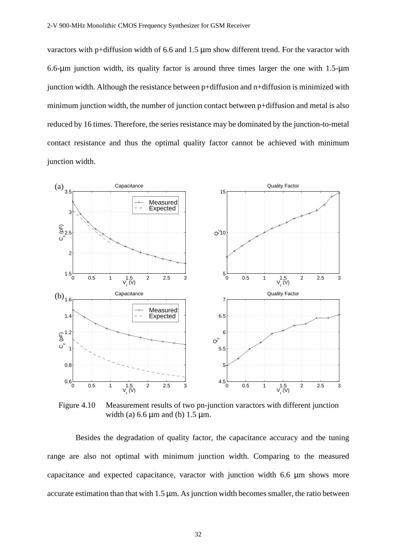
2-V 900-MHz Monolithic CMOS Frequency Synthesizer for GSM Receiver
32
varactors with p+diffusion width of 6.6 and 1.5µm show different trend. For the varactor with
6.6-µm junction width, its quality factor is around three times larger the one with 1.5-µm
junction width. Although the resistance between p+diffusion and n+diffusion is minimized with
minimum junction width, the number of junction contact between p+diffusion and metal is also
reduced by 16 times. Therefore, the series resistance may be dominated by the junction-to-metal
contact resistance and thus the optimal quality factor cannot be achieved with minimum
junction width.
Besides the degradation of quality factor, the capacitance accuracy and the tuning
range are also not optimal with minimum junction width. Comparing to the measured
capacitance and expected capacitance, varactor with junction width 6.6µm shows more
accurate estimation than that with 1.5µm. As junction width becomes smaller, the ratio between
0 0.5 1 1.5 2 2.5 31.5
2
2.5
3
3.5Capacitance
Vr (V)
Cc (
pF)
0 0.5 1 1.5 2 2.5 35
10
15Quality Factor
Vr (V)
Qc
MeasuredExpected
0 0.5 1 1.5 2 2.5 30.6
0.8
1
1.2
1.4
1.6Capacitance
Cc (
pF)
Vr (V)
0 0.5 1 1.5 2 2.5 34.5
5
5.5
6
6.5
7Quality Factor
Qc
Vr (V)
MeasuredExpected
Figure 4.10 Measurement results of two pn-junction varactors with different junctionwidth (a) 6.6µm and (b) 1.5µm.
(b)
(a)
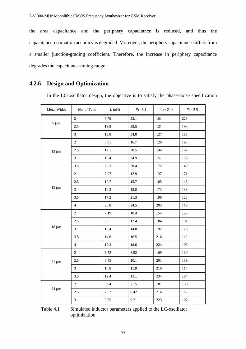
2-V 900-MHz Monolithic CMOS Frequency Synthesizer for GSM Receiver
33
the area capacitance and the periphery capacitance is reduced, and thus the
capacitance-estimation accuracy is degraded. Moreover, the periphery capacitance suffers from
a smaller junction-grading coefficient. Therefore, the increase in periphery capacitance
degrades the capacitance-tuning range.
4.2.6 Design and Optimization
In the LC-oscillator design, the objective is to satisfy the phase-noise specification
Metal Width No. of Turn L (nH) RL (Ω) CS1 (fF) RS1 (Ω)
9 µm2 9.79 23.1 101 228
2.5 13.8 28.5 121 198
3 18.8 34.8 127 185
12 µm
2 8.81 16.7 120 195
2.5 12.1 20.5 144 167
3 16.4 24.9 151 158
3.5 20.2 28.4 172 140
15 µm
2 7.97 12.9 137 171
2.5 10.7 15.7 165 145
3 14.3 18.8 173 138
3.5 17.2 21.3 196 123
4 20.8 24.5 203 119
18 µm
2 7.19 10.4 154 153
2.5 9.5 12.4 184 131
3 12.4 14.8 192 125
3.5 14.6 16.5 216 112
4 17.2 18.6 224 108
21 µm
2 6.53 8.52 169 139
2.5 8.45 10.1 201 119
3 10.8 11.9 210 114
3.5 12.4 13.1 234 104
24 µm2 5.94 7.15 181 130
2.5 7.52 8.42 214 112
3 9.35 9.7 223 107
Table 4.1 Simulated inductor parameters applied to the LC-oscillatoroptimization.

2-V 900-MHz Monolithic CMOS Frequency Synthesizer for GSM Receiver
34
with minimum power consumption. As there is no formula for the calculation of inductance and
series resistance, inductors with different metal width and number of turns are simulated by
ASITIC and the data are shown in Table 4.1. With the simulated inductor parameters, the
capacitance of varactor can then be determined by the required oscillating frequency.
For the pn-junction varactor, the capacitance is modelled by the junction capacitance
in the device model of PMOS transistors. Except for the parasitic capacitance due to the
negative transconductor and the output buffer, the varactor capacitance is maximized to
increase the frequency-tuning range. To achieve a good capacitance-estimation accuracy and a
high quality factor, a junction width of 4.5µm is adopted to keep a balance between N-well and
contact resistance. Moreover, series resistance can be estimated by the measurement results of
the varactor with 6.6-µm junction width in Figure 4.10a.
For the transistorsMn1 in the negative transconductor, its characteristics at different
gate-to-source voltageVgsn1 is taken into account for optimization. Based on the calculation of
0.8 0.9 1 1.1 1.2 1.3 1.4 1.56
8
10
12
14
16
18
20
−124
−124
−124
−124
−124
0.015
0.015
Vgsn1
(V)
L (n
H)
Phase Noise and Power Optimization
Phase Noise = -124 dBc/Hz@600kHzPower < 15 mW
Optimal Point:
(dBc/Hz@600kHz)Phase Noise
Power (mW)
Figure 4.11 Phase-noise and power-consumption optimization of the LC-oscillator.
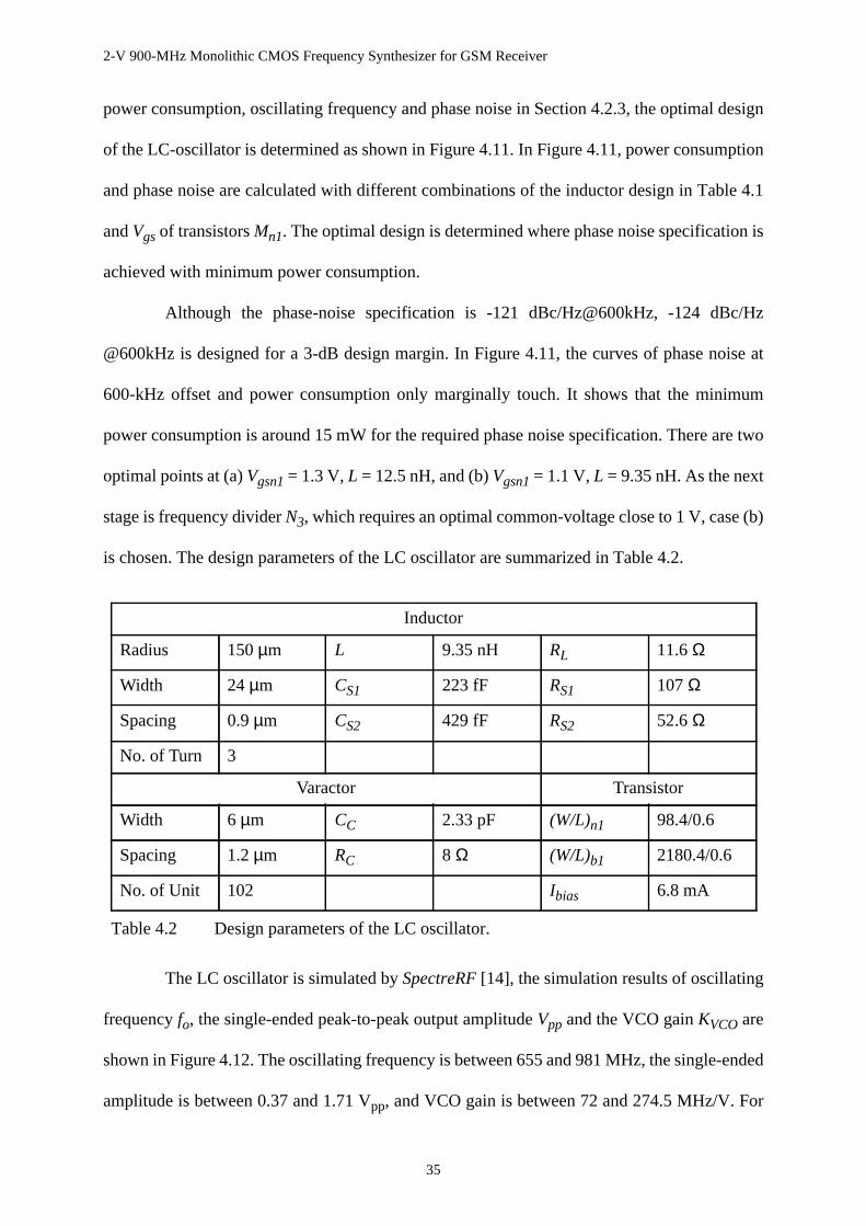
2-V 900-MHz Monolithic CMOS Frequency Synthesizer for GSM Receiver
35
power consumption, oscillating frequency and phase noise in Section 4.2.3, the optimal design
of the LC-oscillator is determined as shown in Figure 4.11. In Figure 4.11, power consumption
and phase noise are calculated with different combinations of the inductor design in Table 4.1
andVgs of transistorsMn1. The optimal design is determined where phase noise specification is
achieved with minimum power consumption.
Although the phase-noise specification is -121 dBc/Hz@600kHz, -124 dBc/Hz
@600kHz is designed for a 3-dB design margin. In Figure 4.11, the curves of phase noise at
600-kHz offset and power consumption only marginally touch. It shows that the minimum
power consumption is around 15 mW for the required phase noise specification. There are two
optimal points at (a)Vgsn1 = 1.3 V,L = 12.5 nH, and (b)Vgsn1 = 1.1 V,L = 9.35 nH. As the next
stage is frequency dividerN3, which requires an optimal common-voltage close to 1 V, case (b)
is chosen. The design parameters of the LC oscillator are summarized in Table 4.2.
The LC oscillator is simulated bySpectreRF[14], the simulation results of oscillating
frequencyfo, the single-ended peak-to-peak output amplitudeVpp and the VCO gainKVCO are
shown in Figure 4.12. The oscillating frequency is between 655 and 981 MHz, the single-ended
amplitude is between 0.37 and 1.71 Vpp, and VCO gain is between 72 and 274.5 MHz/V. For
Inductor
Radius 150µm L 9.35 nH RL 11.6Ω
Width 24µm CS1 223 fF RS1 107Ω
Spacing 0.9µm CS2 429 fF RS2 52.6Ω
No. of Turn 3
Varactor Transistor
Width 6 µm CC 2.33 pF (W/L)n1 98.4/0.6
Spacing 1.2µm RC 8 Ω (W/L)b1 2180.4/0.6
No. of Unit 102 Ibias 6.8 mA
Table 4.2 Design parameters of the LC oscillator.

2-V 900-MHz Monolithic CMOS Frequency Synthesizer for GSM Receiver
36
the phase-noise performance,SpectreRF[14] is used to perform the periodic-steady-state (PSS)
function, the phase-noise simulation results of the LC-oscillator shown in Figure 4.13 is close
to the expected results.
4.3 Frequency dividerN3
0 0.5 1 1.5 2650
700
750
800
850
900
950
1000
889.8 MHz
865.2 MHz
Vc (V)
f o (M
Hz)
0 0.5 1 1.5 2
0.4
0.6
0.8
1
1.2
1.4
1.6
1.8
Vc (V)
Vpp
(V
)
0 0.5 1 1.5 250
100
150
200
250
300
160 MHz/V
Vc (V)
Kvc
o (M
Hz/
V)
Figure 4.12 Oscillating frequency, single-ended peak-to-peak output amplitude andVCO gain of the LC oscillator.
Figure 4.13 Phase-noise simulation results of the LC oscillator bySpectreRF.
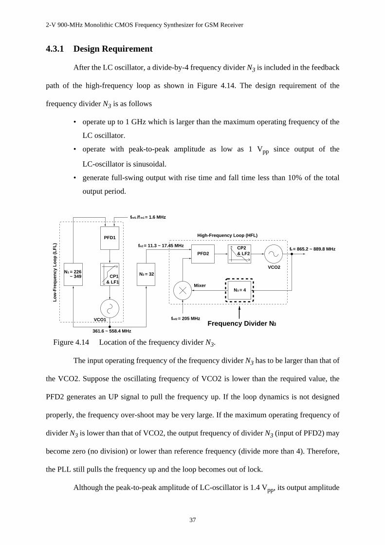
2-V 900-MHz Monolithic CMOS Frequency Synthesizer for GSM Receiver
37
4.3.1 Design Requirement
After the LC oscillator, a divide-by-4 frequency dividerN3 is included in the feedback
path of the high-frequency loop as shown in Figure 4.14. The design requirement of the
frequency dividerN3 is as follows
• operate up to 1 GHz which is larger than the maximum operating frequency of the
LC oscillator.
• operate with peak-to-peak amplitude as low as 1 Vpp since output of the
LC-oscillator is sinusoidal.
• generate full-swing output with rise time and fall time less than 10% of the total
output period.
The input operating frequency of the frequency dividerN3 has to be larger than that of
the VCO2. Suppose the oscillating frequency of VCO2 is lower than the required value, the
PFD2 generates an UP signal to pull the frequency up. If the loop dynamics is not designed
properly, the frequency over-shoot may be very large. If the maximum operating frequency of
dividerN3 is lower than that of VCO2, the output frequency of dividerN3 (input of PFD2) may
become zero (no division) or lower than reference frequency (divide more than 4). Therefore,
the PLL still pulls the frequency up and the loop becomes out of lock.
Although the peak-to-peak amplitude of LC-oscillator is 1.4 Vpp, its output amplitude
fref2 = 205 MHz
fo = 865.2 ~ 889.8 MHz
2 = 32N
fin2 = 11.3 ~ 17.45 MHz
N = 2261
~ 349
fref1 /f in1 = 1.6 MHz
Frequency Divider N 3
Mixer3 = 4
High-Frequency Loop (HFL)
361.6 ~ 558.4 MHz
VCO1
Low
-Fre
quen
cy L
oop
(LF
L)
N
VCO2
CP1& LF1
PFD1
& LF2CP2
PFD2
Figure 4.14 Location of the frequency dividerN3.
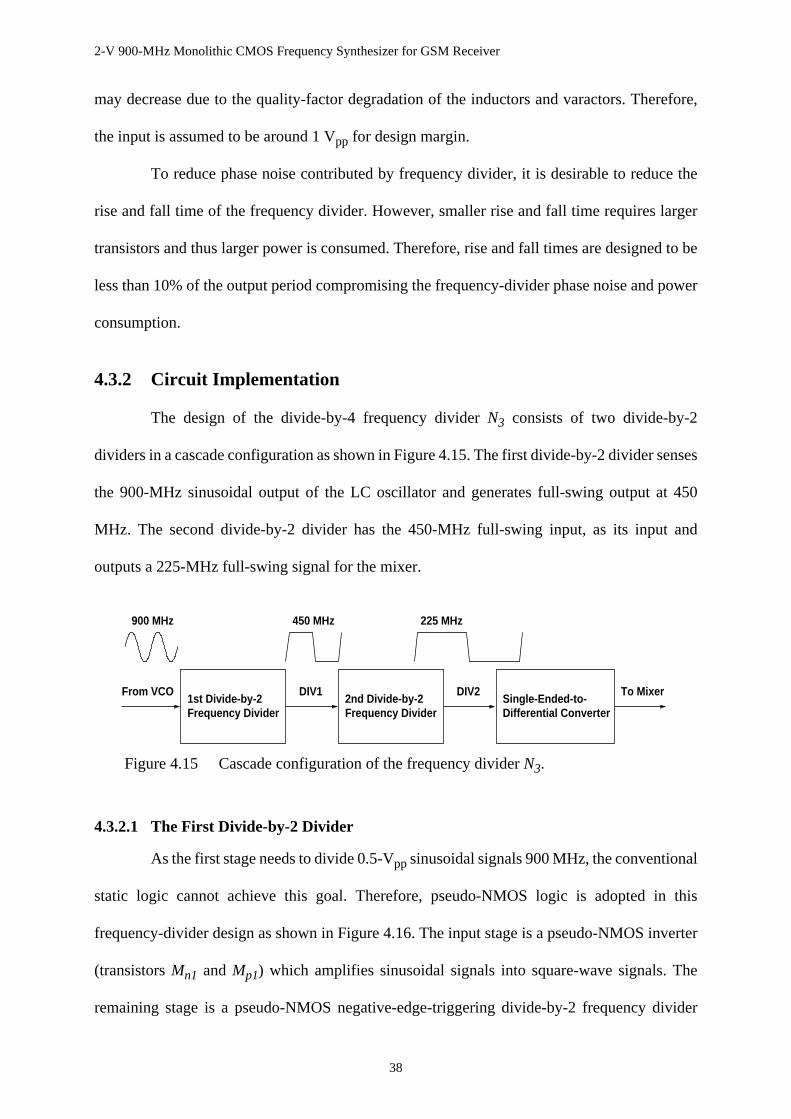
2-V 900-MHz Monolithic CMOS Frequency Synthesizer for GSM Receiver
38
may decrease due to the quality-factor degradation of the inductors and varactors. Therefore,
the input is assumed to be around 1 Vpp for design margin.
To reduce phase noise contributed by frequency divider, it is desirable to reduce the
rise and fall time of the frequency divider. However, smaller rise and fall time requires larger
transistors and thus larger power is consumed. Therefore, rise and fall times are designed to be
less than 10% of the output period compromising the frequency-divider phase noise and power
consumption.
4.3.2 Circuit Implementation
The design of the divide-by-4 frequency dividerN3 consists of two divide-by-2
dividers in a cascade configuration as shown in Figure 4.15. The first divide-by-2 divider senses
the 900-MHz sinusoidal output of the LC oscillator and generates full-swing output at 450
MHz. The second divide-by-2 divider has the 450-MHz full-swing input, as its input and
outputs a 225-MHz full-swing signal for the mixer.
4.3.2.1 The First Divide-by-2 Divider
As the first stage needs to divide 0.5-Vpp sinusoidal signals 900 MHz, the conventional
static logic cannot achieve this goal. Therefore, pseudo-NMOS logic is adopted in this
frequency-divider design as shown in Figure 4.16. The input stage is a pseudo-NMOS inverter
(transistorsMn1 andMp1) which amplifies sinusoidal signals into square-wave signals. The
remaining stage is a pseudo-NMOS negative-edge-triggering divide-by-2 frequency divider
1st Divide-by-2Frequency Divider
2nd Divide-by-2Frequency Divider
Single-Ended-to-Differential Converter
225 MHz
From VCO DIV1 DIV2 To Mixer
450 MHz900 MHz
Figure 4.15 Cascade configuration of the frequency dividerN3.
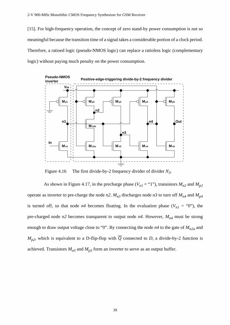
2-V 900-MHz Monolithic CMOS Frequency Synthesizer for GSM Receiver
39
[15]. For high-frequency operation, the concept of zero stand-by power consumption is not so
meaningful because the transition time of a signal takes a considerable portion of a clock period.
Therefore, a ratioed logic (pseudo-NMOS logic) can replace a ratioless logic (complementary
logic) without paying much penalty on the power consumption.
As shown in Figure 4.17, in the precharge phase (Vn1 = “1”), transistorsMn2 andMp2
operate as inverter to pre-charge the noden2. Mn3 discharges noden3 to turn offMn4 andMp4
is turned off, so that noden4 becomes floating. In the evaluation phase (Vn1 = “0”), the
pre-charged noden2 becomes transparent to output noden4. However,Mn4 must be strong
enough to draw output voltage close to “0”. By connecting the noden4 to the gate ofMn2a and
Mp2, which is equivalent to a D-flip-flop withQ connected toD, a divide-by-2 function is
achieved. TransistorsMn5 andMp5 form an inverter to serve as an output buffer.
Pseudo-NMOSinverter
Mn1 Mn2a Mn4 Mn5Mn3
Mp2 Mp3 Mp4 Mp5Mp1
Vdd
Mn2b
Positive-edge-triggering divide-by-2 frequency divider
In
Out
n2
n3
n4n1
Figure 4.16 The first divide-by-2 frequency divider of dividerN3.
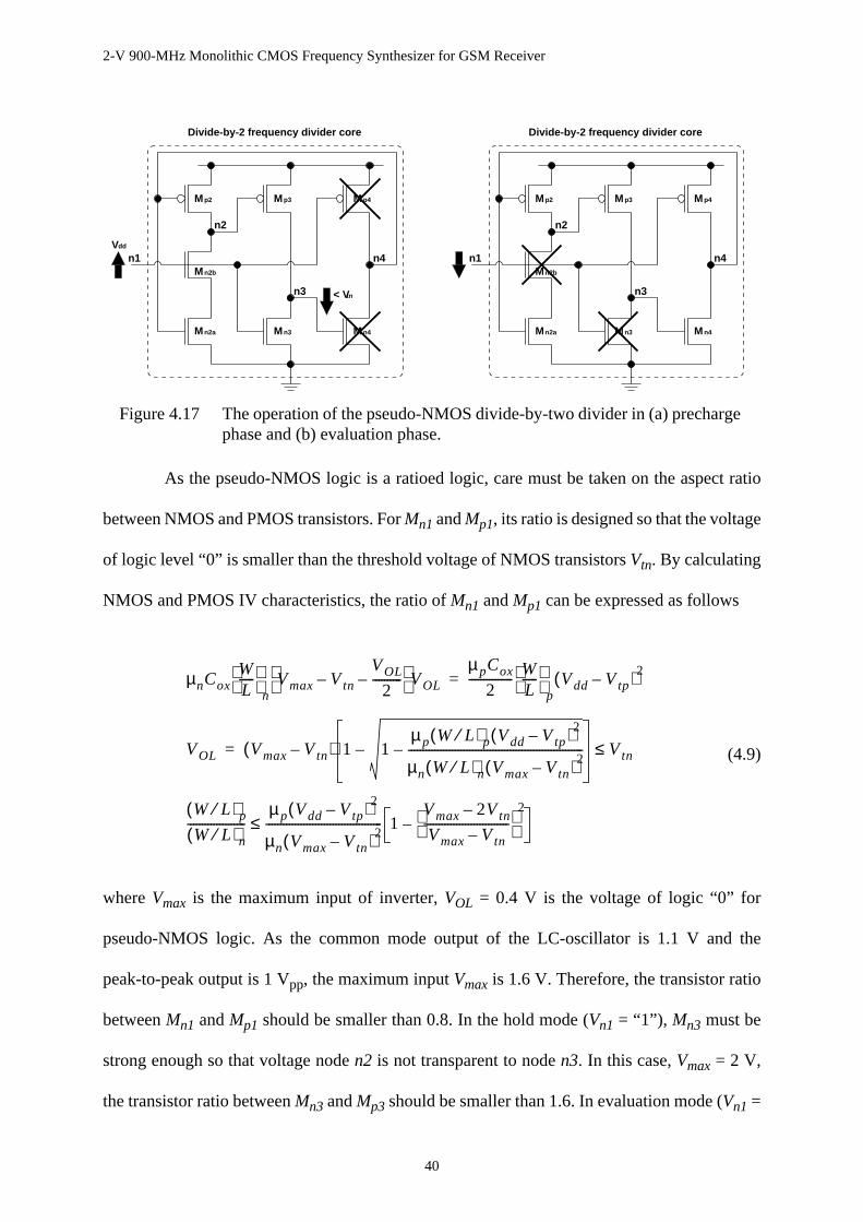
2-V 900-MHz Monolithic CMOS Frequency Synthesizer for GSM Receiver
40
As the pseudo-NMOS logic is a ratioed logic, care must be taken on the aspect ratio
between NMOS and PMOS transistors. ForMn1 andMp1, its ratio is designed so that the voltage
of logic level “0” is smaller than the threshold voltage of NMOS transistorsVtn. By calculating
NMOS and PMOS IV characteristics, the ratio ofMn1 andMp1 can be expressed as follows
(4.9)
whereVmax is the maximum input of inverter,VOL = 0.4 V is the voltage of logic “0” for
pseudo-NMOS logic. As the common mode output of the LC-oscillator is 1.1 V and the
peak-to-peak output is 1 Vpp, the maximum inputVmax is 1.6 V. Therefore, the transistor ratio
betweenMn1 andMp1 should be smaller than 0.8. In the hold mode (Vn1 = “1”), Mn3 must be
strong enough so that voltage noden2 is not transparent to noden3. In this case,Vmax = 2 V,
the transistor ratio betweenMn3 andMp3 should be smaller than 1.6. In evaluation mode (Vn1 =
Mn2a Mn4Mn3
Mp2 Mp3 Mp4
Mn2b
< Vtn
Vdd
n2
n3
n4n1
Divide-by-2 frequency divider core
Mn2a Mn4Mn3
Mp2 Mp3 Mp4
Mn2b
n2
n3
n4n1
Divide-by-2 frequency divider core
Figure 4.17 The operation of the pseudo-NMOS divide-by-two divider in (a) prechargephase and (b) evaluation phase.
µnCoxWL-----
n
Vmax Vtn–VOL
2----------–
VOL
µpCox
2--------------- W
L-----
p
Vdd Vtp–( )2=
VOL Vmax Vtn–( ) 1 1µp W L⁄( )p Vdd Vtp–( )2
µn W L⁄( )n Vmax Vtn–( )2------------------------------------------------------------–– Vtn≤=
W L⁄( )p
W L⁄( )n--------------------
µp Vdd Vtp–( )2
µn Vmax Vtn–( )2---------------------------------------- 1
Vmax 2Vtn–
Vmax Vtn–-----------------------------
2–≤

2-V 900-MHz Monolithic CMOS Frequency Synthesizer for GSM Receiver
41
“0”), Mn4 must be large enough to obtainVOL at noden4, the ratio betweenMn4 andMp4 should
be smaller than 1.6.
4.3.2.2 The Second Divide-by-2 Divider
As the first divide-by-2 frequency divider has already divided the input sinusoidal
signals into full-swing output, the second divide-by-2 has relaxed speed (500 MHz) and input
amplitude (full swing) requirement. True-Single-Phase-Clock (TSPC) Logic can construct an
edge-triggering D-flip-flop with only 9 transistors, the reduced transistor parasitics enhances
the high-speed low-power operation up to several hundreds mega hertz [16]. Therefore, TSPC
Logic is adopted for the second-divider implementation as shown in Figure 4.18.
The operation of the TSPC divider is as shown in Figure 4.19. In the precharge phase
(Vclk = “0”), noden1 is pre-charged to a value depending on the input signal and noden2 is
pre-charged toVdd. As transistorsMn3b andMp3 are turned off, noden3 becomes floating. In
the evaluation mode, if noden1 is pre-charged toVdd, noden2 is discharged andVn3 is pulled
up by transistorMp3. If noden1 is precharged to “0”, noden2 is not discharged, and noden3 is
pulled down by transistorsMn3a andMn3b.
Mn4
Mp4Mp3
Mn3a
Mn3b
Mp2
Mn2b
Mn2aMn1
Mp1a
Mp1b
Vdd
Out
n1
n2 n3
CLK
CLK
CLK
Figure 4.18 True-Single-Phase-Clock (TSPC) divide-by-2 frequency divider.
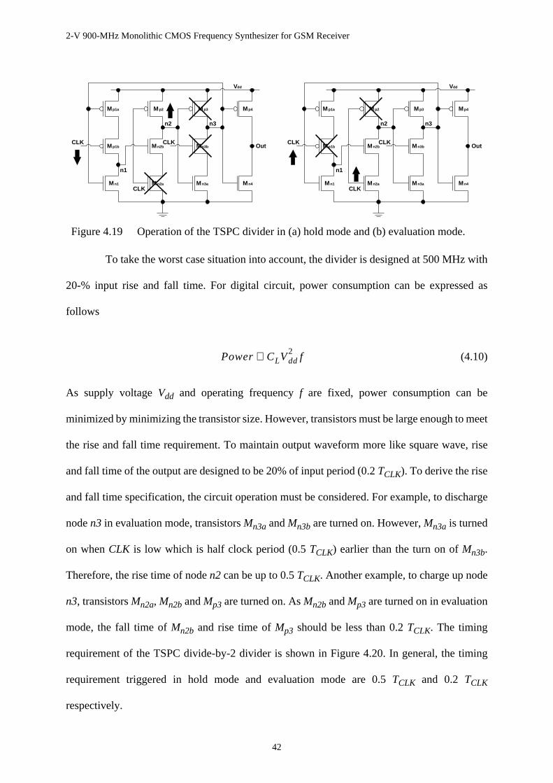
2-V 900-MHz Monolithic CMOS Frequency Synthesizer for GSM Receiver
42
To take the worst case situation into account, the divider is designed at 500 MHz with
20-% input rise and fall time. For digital circuit, power consumption can be expressed as
follows
(4.10)
As supply voltageVdd and operating frequencyf are fixed, power consumption can be
minimized by minimizing the transistor size. However, transistors must be large enough to meet
the rise and fall time requirement. To maintain output waveform more like square wave, rise
and fall time of the output are designed to be 20% of input period (0.2TCLK). To derive the rise
and fall time specification, the circuit operation must be considered. For example, to discharge
noden3 in evaluation mode, transistorsMn3a andMn3b are turned on. However,Mn3a is turned
on whenCLK is low which is half clock period (0.5TCLK) earlier than the turn on ofMn3b.
Therefore, the rise time of noden2 can be up to 0.5TCLK. Another example, to charge up node
n3, transistorsMn2a, Mn2b andMp3 are turned on. AsMn2b andMp3 are turned on in evaluation
mode, the fall time ofMn2b and rise time ofMp3 should be less than 0.2TCLK. The timing
requirement of the TSPC divide-by-2 divider is shown in Figure 4.20. In general, the timing
requirement triggered in hold mode and evaluation mode are 0.5TCLK and 0.2 TCLK
respectively.
Mn4
Mp4Mp3
Mn3a
Mn3b
Mp2
Mn2b
Mn2aMn1
Mp1a
Mp1b
Vdd
Out
n1
n2 n3
CLK
CLK
CLK
Mn4
Mp4Mp3
Mn3a
Mn3b
Mp2
Mn2b
Mn2aMn1
Mp1a
Mp1b
Vdd
Out
n1
n2 n3
CLK
CLK
CLK
Figure 4.19 Operation of the TSPC divider in (a) hold mode and (b) evaluation mode.
Power CLVdd2
f∝
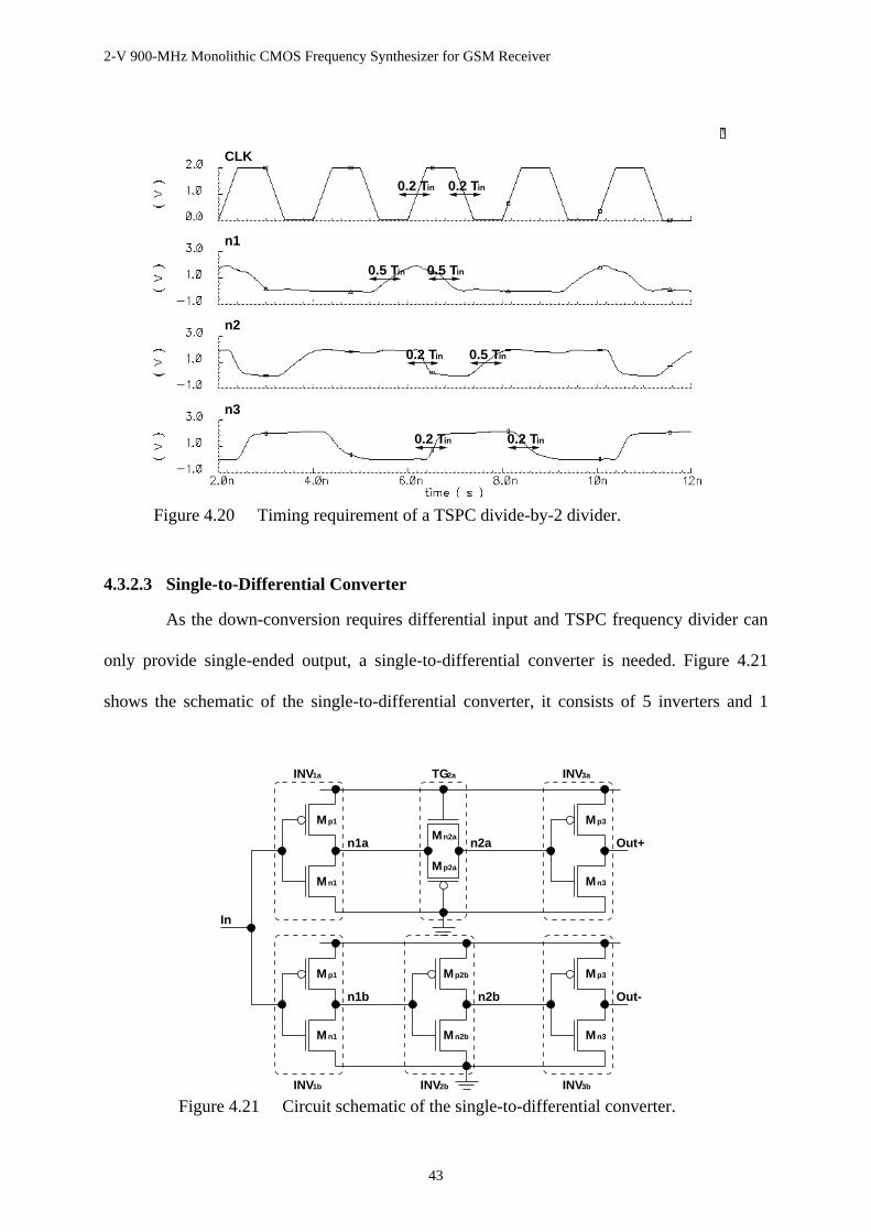
2-V 900-MHz Monolithic CMOS Frequency Synthesizer for GSM Receiver
43
4.3.2.3 Single-to-Differential Converter
As the down-conversion requires differential input and TSPC frequency divider can
only provide single-ended output, a single-to-differential converter is needed. Figure 4.21
shows the schematic of the single-to-differential converter, it consists of 5 inverters and 1
in
0.5 Tin0.5 Tin
0.5 T
0.2 T
0.2 Tin0.2 Tin
in
in
in0.2 T
0.2 T
CLK
n1
n2
n3
Figure 4.20 Timing requirement of a TSPC divide-by-2 divider.
Mp1
Mn2b
Mp2b
Mn1
Mp3
Mn3
Mp1
Mn1
Mp2a
Mn2a
Mn3
Mp3
TG2a
INV2bINV1b INV3b
INV3aINV1a
n1b
n1a n2a
n2b
Out+
Out-
In
Figure 4.21 Circuit schematic of the single-to-differential converter.
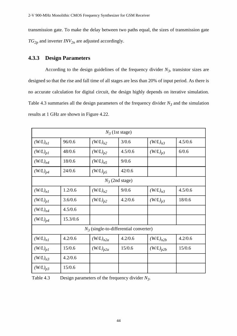
2-V 900-MHz Monolithic CMOS Frequency Synthesizer for GSM Receiver
44
transmission gate. To make the delay between two paths equal, the sizes of transmission gate
TG2p and inverterINV2n are adjusted accordingly.
4.3.3 Design Parameters
According to the design guidelines of the frequency dividerN3, transistor sizes are
designed so that the rise and fall time of all stages are less than 20% of input period. As there is
no accurate calculation for digital circuit, the design highly depends on iterative simulation.
Table 4.3 summaries all the design parameters of the frequency dividerN3 and the simulation
results at 1 GHz are shown in Figure 4.22.
N3 (1st stage)
(W/L)n1 96/0.6 (W/L)n2 3/0.6 (W/L)n3 4.5/0.6
(W/L)p1 48/0.6 (W/L)p2 4.5/0.6 (W/L)p3 6/0.6
(W/L)n4 18/0.6 (W/L)n5 9/0.6
(W/L)p4 24/0.6 (W/L)p5 42/0.6
N3 (2nd stage)
(W/L)n1 1.2/0.6 (W/L)n2 9/0.6 (W/L)n3 4.5/0.6
(W/L)p1 3.6/0.6 (W/L)p2 4.2/0.6 (W/L)p3 18/0.6
(W/L)n4 4.5/0.6
(W/L)p4 15.3/0.6
N3 (single-to-differential converter)
(W/L)n1 4.2/0.6 (W/L)n2a 4.2/0.6 (W/L)n2b 4.2/0.6
(W/L)p1 15/0.6 (W/L)p2a 15/0.6 (W/L)p2b 15/0.6
(W/L)n3 4.2/0.6
(W/L)p3 15/0.6
Table 4.3 Design parameters of the frequency dividerN3.

2-V 900-MHz Monolithic CMOS Frequency Synthesizer for GSM Receiver
45
4.4 Down-Conversion Mixer
4.4.1 Design Requirement
After the frequency dividerN3, a down-conversion mixer, which is illustrated in Figure
4.23, operates together with the second reference signalfref2 to generate the frequency shift
N3fref2. The design requirement of the down-conversion mixer is as follows
• operate at frequency up to 250 MHz for both inputs.
• output bandwidth is at 10 MHz to eliminate high frequency glitches.
• generate full-swing output to drive the PFD.
As the input signals of the mixer are from the frequency divider N3 and the second reference
signal, the maximum operating frequency is up to 250 MHz. When the high-frequency loop
locks, the output frequency of the mixer ranges from 11.3 MHz to 17.45 MHz, so output
bandwidth is designed at 10 MHz to eliminate output glitches. Since both inputs are full swing,
DIV2
DIV1
Out+
Out-
CLK
Figure 4.22 Simulation results of the whole frequency dividerN3.
Out+
CLK
DIV1
DIV2
Out-

2-V 900-MHz Monolithic CMOS Frequency Synthesizer for GSM Receiver
46
all the input devices act as switches. Moreover, because there is no adjacent-channel
interference as the mixer in receiver front-end, the linearity of the mixer is not critical. Similar
to frequency divider, phase noise contributed by mixer is insignificant if output rise and fall
times are short enough.
4.4.2 Circuit Implementation
The mixer shown in Figure 4.24 consists of a Gilbert-cell mixer, a low-pass filter and
a differential-to-single-ended buffer. The Gilbert-cell mixer formed by transistorsMn1 andMn2
performs the mixing function, and the high frequency tones are filtered by the low-pass filter
formed byRL andCL. In order to drive the PFD, output of the Gilbert-cell mixer is effectively
amplified by the differential-to-single-ended buffer to a full-swing output.
fref2 = 205 MHz
fo = 865.2 ~ 889.8 MHz
2 = 32N
fin2 = 11.3 ~ 17.45 MHz
N = 2261
~ 349
fref1 /f in1 = 1.6 MHz
LF1
3 = 4
LF2
High-Frequency Loop (HFL)
361.6 ~ 558.4 MHz
VCO1
Low
-Fre
quen
cy L
oop
(LF
L)
PFD1
PFD2
& CP1
& CP2
N
VCO2
Down-Conversion Mixer
Figure 4.23 Location of the down-conversion mixer.

2-V 900-MHz Monolithic CMOS Frequency Synthesizer for GSM Receiver
47
4.4.3 Design Issues
As the output bandwidth is designed to be 10 MHz, load capacitanceCL and resistance
RL are determined based on the chip-area optimization. In order to provide appropriate input
amplitude and gate bias for the transistorsMp1, the bias currentIbias is designed accordingly.
For input transistorsMn1 andMn2, their aspect ratio is designed to keep the drain-to-source
voltageVds to be less than 0.1 V. All the design parameters of the mixer are summarized in
Table 4.4.
Mb1 Mb1
Mn1 Mn1 Ibias
n2M n2M n2M n2M
p1M p1M
n3M n3M
CL CL RLRL
Vdd
Gilbert Cell
Low-Pass Filter
Out
n1+ n1-
In1+ In1-
In2+ In2- In2+
Differential-to-Single-Ended Buffer
Figure 4.24 Circuit implementation of the down-conversion mixer.
(W/L)n1 15/0.6 (W/L)n2 15/0.6 (W/L)b1 30/1.2
(W/L)p1 6/0.6 (W/L)n3 1.5/0.6 Ibias 32 µA
RL 70 kΩ CL 2 pF
Table 4.4 Design parameters of the down-conversion mixer.
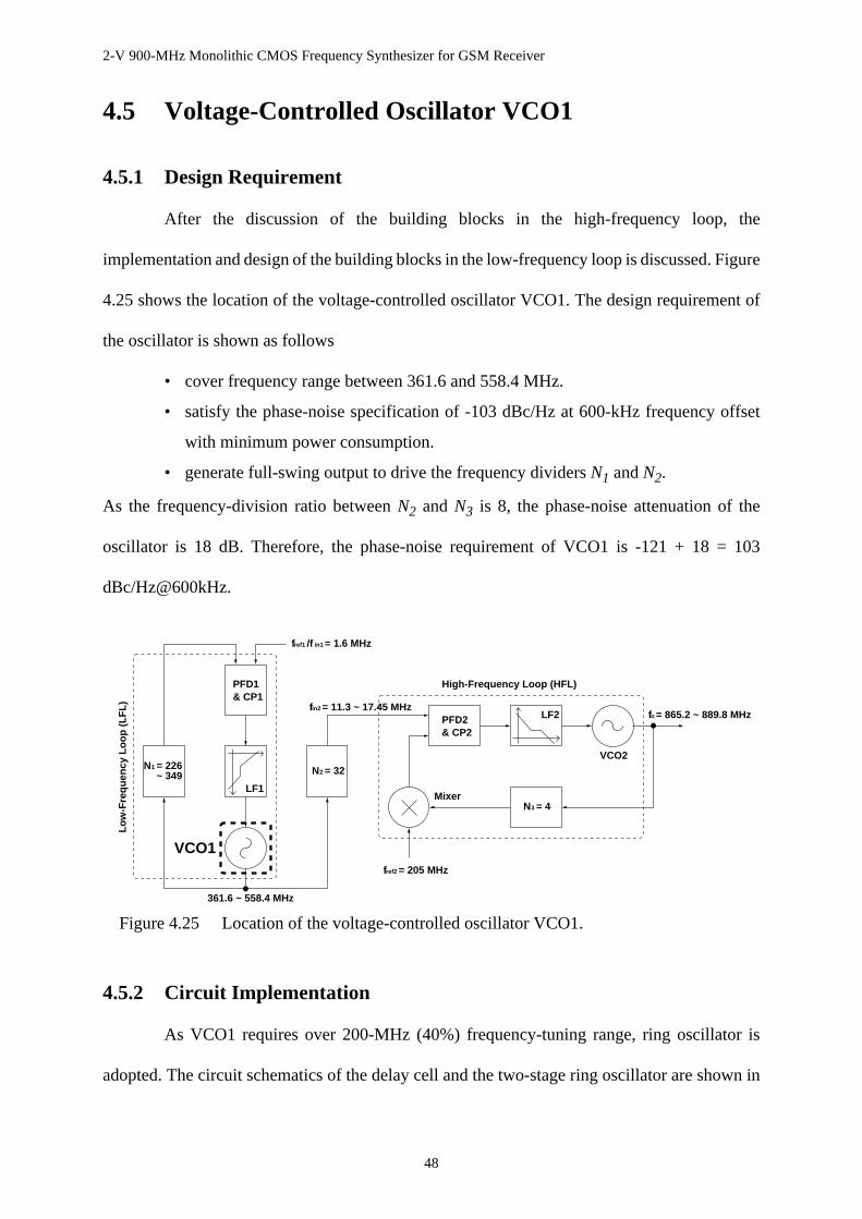
2-V 900-MHz Monolithic CMOS Frequency Synthesizer for GSM Receiver
48
4.5 Voltage-Controlled Oscillator VCO1
4.5.1 Design Requirement
After the discussion of the building blocks in the high-frequency loop, the
implementation and design of the building blocks in the low-frequency loop is discussed. Figure
4.25 shows the location of the voltage-controlled oscillator VCO1. The design requirement of
the oscillator is shown as follows
• cover frequency range between 361.6 and 558.4 MHz.
• satisfy the phase-noise specification of -103 dBc/Hz at 600-kHz frequency offset
with minimum power consumption.
• generate full-swing output to drive the frequency dividersN1 andN2.
As the frequency-division ratio betweenN2 andN3 is 8, the phase-noise attenuation of the
oscillator is 18 dB. Therefore, the phase-noise requirement of VCO1 is -121 + 18 = 103
dBc/Hz@600kHz.
4.5.2 Circuit Implementation
As VCO1 requires over 200-MHz (40%) frequency-tuning range, ring oscillator is
adopted. The circuit schematics of the delay cell and the two-stage ring oscillator are shown in
fref2 = 205 MHz
fo = 865.2 ~ 889.8 MHz
2 = 32N
fin2 = 11.3 ~ 17.45 MHz
N = 2261
~ 349
fref1 /f in1 = 1.6 MHz
MixerLF1
3 = 4
LF2
High-Frequency Loop (HFL)
361.6 ~ 558.4 MHz
Low
-Fre
quen
cy L
oop
(LF
L)
PFD1
PFD2
& CP1
& CP2
N
VCO2
VCO1
Figure 4.25 Location of the voltage-controlled oscillator VCO1.
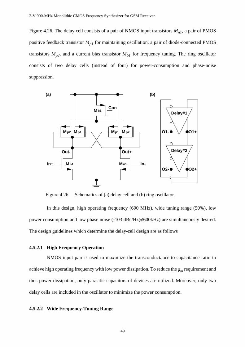
2-V 900-MHz Monolithic CMOS Frequency Synthesizer for GSM Receiver
49
Figure 4.26. The delay cell consists of a pair of NMOS input transistorsMn1, a pair of PMOS
positive feedback transistorMp1 for maintaining oscillation, a pair of diode-connected PMOS
transistorsMp2, and a current bias transistorMb1 for frequency tuning. The ring oscillator
consists of two delay cells (instead of four) for power-consumption and phase-noise
suppression.
In this design, high operating frequency (600 MHz), wide tuning range (50%), low
power consumption and low phase noise (-103 dBc/Hz@600kHz) are simultaneously desired.
The design guidelines which determine the delay-cell design are as follows
4.5.2.1 High Frequency Operation
NMOS input pair is used to maximize the transconductance-to-capacitance ratio to
achieve high operating frequency with low power dissipation. To reduce thegm requirement and
thus power dissipation, only parasitic capacitors of devices are utilized. Moreover, only two
delay cells are included in the oscillator to minimize the power consumption.
4.5.2.2 Wide Frequency-Tuning Range
Mn1 Mn1
Mp1 Mp2Mp2 Mp1
Mb1
(a) (b)
In+ In-
Con
Out- Out+
O1-
O2+O2-
Delay#1
Delay#2
O1+
Figure 4.26 Schematics of (a) delay cell and (b) ring oscillator.
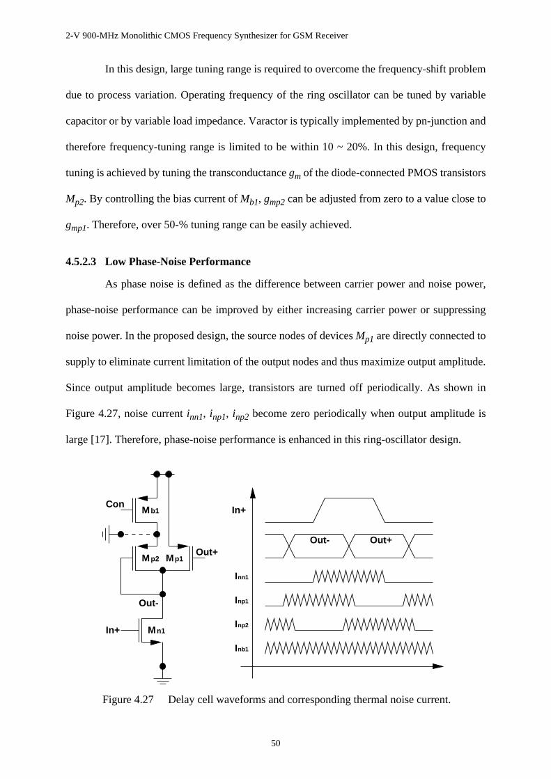
2-V 900-MHz Monolithic CMOS Frequency Synthesizer for GSM Receiver
50
In this design, large tuning range is required to overcome the frequency-shift problem
due to process variation. Operating frequency of the ring oscillator can be tuned by variable
capacitor or by variable load impedance. Varactor is typically implemented by pn-junction and
therefore frequency-tuning range is limited to be within 10 ~ 20%. In this design, frequency
tuning is achieved by tuning the transconductancegm of the diode-connected PMOS transistors
Mp2. By controlling the bias current ofMb1, gmp2 can be adjusted from zero to a value close to
gmp1. Therefore, over 50-% tuning range can be easily achieved.
4.5.2.3 Low Phase-Noise Performance
As phase noise is defined as the difference between carrier power and noise power,
phase-noise performance can be improved by either increasing carrier power or suppressing
noise power. In the proposed design, the source nodes of devicesMp1 are directly connected to
supply to eliminate current limitation of the output nodes and thus maximize output amplitude.
Since output amplitude becomes large, transistors are turned off periodically. As shown in
Figure 4.27, noise currentinn1, inp1, inp2 become zero periodically when output amplitude is
large [17]. Therefore, phase-noise performance is enhanced in this ring-oscillator design.
nn1I
np1I
np2I
nb1I
In+
Out- Out+
Mn1
Mp2 Mp1
Mb1
In+
Out-
Con
Out+
Figure 4.27 Delay cell waveforms and corresponding thermal noise current.
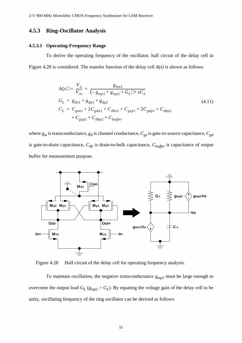
2-V 900-MHz Monolithic CMOS Frequency Synthesizer for GSM Receiver
51
4.5.3 Ring-Oscillator Analysis
4.5.3.1 Operating-Frequency Range
To derive the operating frequency of the oscillator, half circuit of the delay cell in
Figure 4.28 is considered. The transfer function of the delay cellA(s) is shown as follows
(4.11)
wheregm is transconductance,gd is channel conductance,Cgs is gate-to-source capacitance,Cgd
is gate-to-drain capacitance,Cdb is drain-to-bulk capacitance,Cbuffer is capacitance of output
buffer for measurement purpose.
To maintain oscillation, the negative transconductancegmp1 must be large enough to
overcome the output loadGL (gmp1 > GL). By equating the voltage gain of the delay cell to be
unity, oscillating frequency of the ring oscillator can be derived as follows
A s( )Vo
Vin--------
gmn1
gmp1– gmp2 GL+ +( ) sCL+--------------------------------------------------------------------= =
GL gdn1 gdp1 gdp2+ +=
CL Cgsn1 2Cgdn1 Cdbn1 Cgsp1 2Cgdp1 Cdbp1+ + + + +=
Cgsp2 Cdbp2 Cbuffer+ + +
Mn1 Mn1
Mp1 Mp2Mp2 Mp1
Mb1
In+ In-
Con
Out- Out+gmn1Vin C L
gmp1Vogmp2G L
-Vo
Figure 4.28 Half circuit of the delay cell for operating frequency analysis.

2-V 900-MHz Monolithic CMOS Frequency Synthesizer for GSM Receiver
52
(4.12)
By controlling thegm of diode-connected PMOS devicesMp2, oscillating frequency
fosc can be tuned. At the maximum oscillating frequencyfmax, negative transconductancegmp1
is just large enough to completely compensate the loadGL (gmp1 = GL). At the minimum
oscillating frequencyfmin, diode-connected PMOS transistorsMp2 are turned off (gmp2 = 0).
Then, maximum frequencyfmax, minimum frequencyfmin and operating frequency rangefrange
can be calculated.
(4.13)
The maximum oscillating frequency is proportional togmn1/CL. Therefore, NMOS input
devices are adopted to reduce the corresponding power consumption. From (4.13), 50-%
frequency-tuning range can be achieved with transconductance ratio between transistorsMn1
andMp1 to be .
4.5.3.2 Phase-Noise Analysis
Phase-noise analysis of the ring oscillator is performed based on the ring-oscillator
analysis by Ali Hajimiri [18]. Approximate impulse-stimulus function (ISF) of ring oscillator is
shown in Figure 4.29. Single-side-band phase noiseLVCO2 ∆ω of the two-stage ring oscillator
can then be calculated as follows
f osc1
2π------
gmn12
gmp1– gmp2 GL+ +( )2–
CL2
------------------------------------------------------------------------=
f max1
2π------
gmn1
CL-----------⋅≈ f min
12π------
gmn12
gmp12
–
CL2
-----------------------------⋅≈
f range f max 1 1gmp1
gmn1-----------
2––
⋅≈
gmp1 gmn1⁄ 3 4⁄=

2-V 900-MHz Monolithic CMOS Frequency Synthesizer for GSM Receiver
53
(4.14)
whereΓrms is root-mean square of ISF,N = 4 is the number of noise sources,∆ω is frequency
offset for phase-noise analysis,Vp is the peak output amplitude, and is total device noise-
power-spectral density. Calculation shows that the phase noise is approximately -107 dBc/Hz
at 600-kHz offset.
4.5.4 Design Optimization
Based on the analysis of frequency range and phase noise in Section 4.5.3.1 and
Section 4.5.3.2, design optimization of the ring oscillator is done. To reduce parasitic
capacitance, all transistors are designed with minimum channel length. In order to achieve the
maximum operating frequency, current of transistorsMp1 andMp2 are equal. As shown in
Figure 4.30, the maximum operating frequency, tuning range and phase noise at 600-kHz
frequency offset are plotted at differentWn1 andVgsn1.
Γrms2 2
π--- x
2xd
0
π 2⁄∫ π2
12------= =
LVCO2 ∆ω NΓrms
2
2 ∆ω2⋅------------------
in2 ∆f⁄
CL2Vp
2--------------⋅ ⋅=
in2 ∆f⁄
2π
(x )Γ
Γrms2
=π2
12
π 2πx
Figure 4.29 Approximate ISF for the ring-oscillator phase-noise analysis.

2-V 900-MHz Monolithic CMOS Frequency Synthesizer for GSM Receiver
54
The optimal design solution is found at the point with 600-MHz maximum operating
frequency and 50-% tuning range. At that point, phase noise, which is relatively insensitive to
Wn1 andVgsn1, is -106.5 dBc/Hz@600kHz. As supply voltage and current of transistorsMp1 and
Mp2 are equal, all the other transistors can be determined byWn1. Table 4.5 summaries all the
design parameters of the ring oscillator core VCO1 and inverter buffers.
The ring oscillator is simulated bySpectreRF, the simulation results of oscillating
frequencyfo, VCO gainKvco and power consumption are shown in Figure 4.31. The oscillating
frequency is between 303.6 and 595.6 MHz, single-ended peak-to-peak amplitude is between
0.8 0.82 0.84 0.86 0.88 0.9 0.92 0.94 0.96 0.98 1
5
10
15
20
25
30
35
40
45
6e+08 50
−107
−107
−107
−106
Vgsn1
(V)
Wn1
(um
)Design Optimization
max (MHz)
Phase Noise(dBc/Hz@600kHz)
Optimal Point:ftuning Range = 50 %Phase Noise = -106.5 dBc/Hz@600kHz
f
= 600 MHzmax
Tuning Range (%)
Figure 4.30 Design optimization of the ring oscillator VCO1.
Oscillator Core Output Buffer
(W/L)n1 30/0.6 (W/L)p1 51.6/0.6 (W/L)bn1 16.8/0.6
(W/L)p2 51.6/0.6 (W/L)b1 110.4/0.6 (W/L)bp1 48/0.6
Table 4.5 Design parameters of the ring oscillator VCO1.
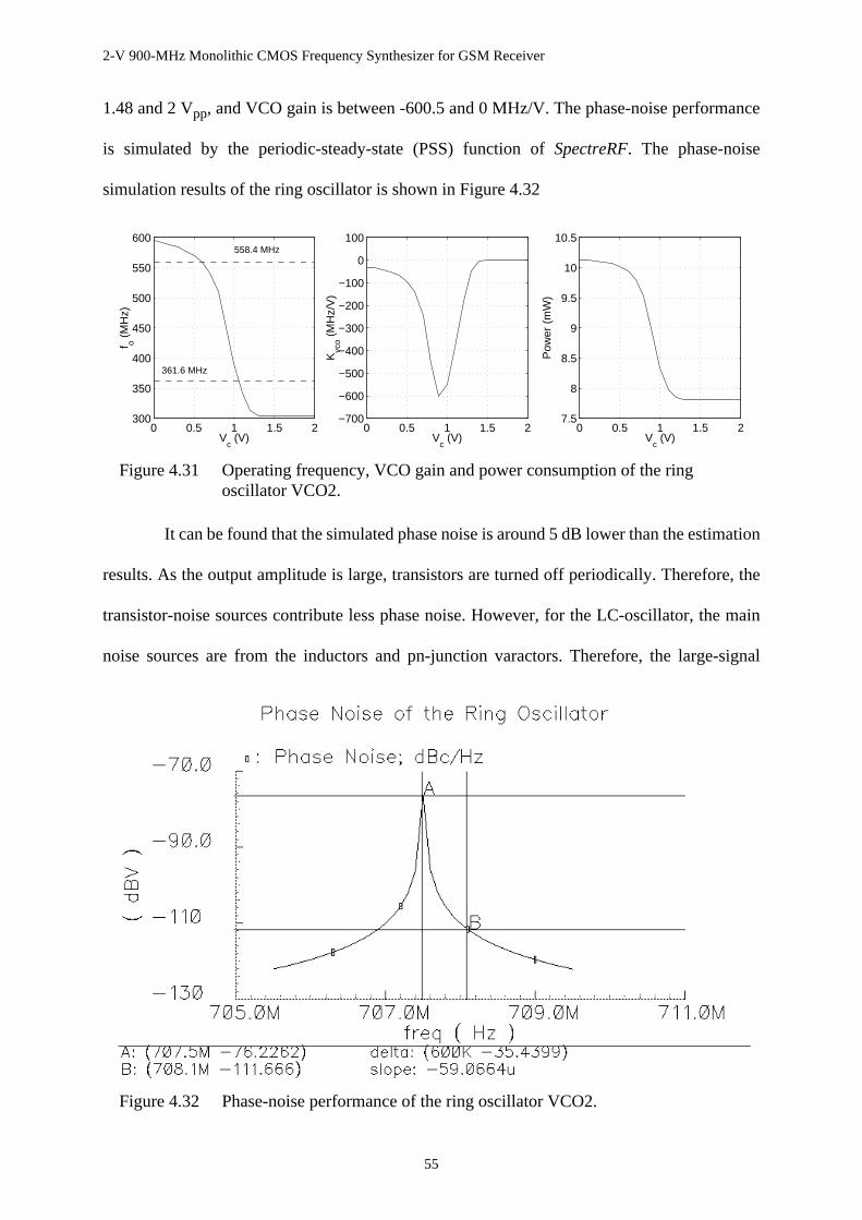
2-V 900-MHz Monolithic CMOS Frequency Synthesizer for GSM Receiver
55
1.48 and 2 Vpp, and VCO gain is between -600.5 and 0 MHz/V. The phase-noise performance
is simulated by the periodic-steady-state (PSS) function ofSpectreRF. The phase-noise
simulation results of the ring oscillator is shown in Figure 4.32
It can be found that the simulated phase noise is around 5 dB lower than the estimation
results. As the output amplitude is large, transistors are turned off periodically. Therefore, the
transistor-noise sources contribute less phase noise. However, for the LC-oscillator, the main
noise sources are from the inductors and pn-junction varactors. Therefore, the large-signal
0 0.5 1 1.5 2300
350
400
450
500
550
600558.4 MHz
361.6 MHz
Vc (V)
f o (M
Hz)
0 0.5 1 1.5 2−700
−600
−500
−400
−300
−200
−100
0
100
Vc (V)
Kvc
o (M
Hz/
V)
0 0.5 1 1.5 27.5
8
8.5
9
9.5
10
10.5
Vc (V)
Pow
er (
mW
)
Figure 4.31 Operating frequency, VCO gain and power consumption of the ringoscillator VCO2.
Figure 4.32 Phase-noise performance of the ring oscillator VCO2.
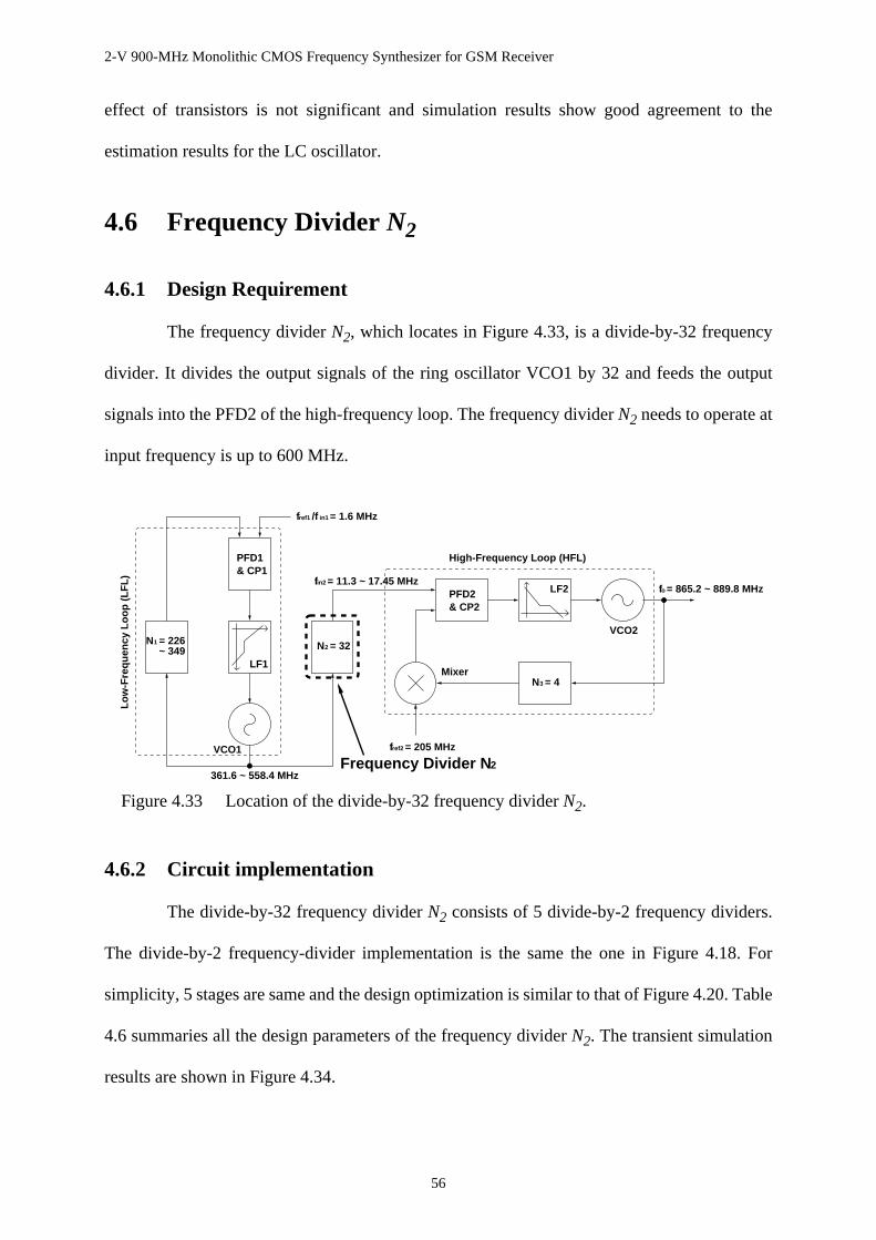
2-V 900-MHz Monolithic CMOS Frequency Synthesizer for GSM Receiver
56
effect of transistors is not significant and simulation results show good agreement to the
estimation results for the LC oscillator.
4.6 Frequency DividerN2
4.6.1 Design Requirement
The frequency dividerN2, which locates in Figure 4.33, is a divide-by-32 frequency
divider. It divides the output signals of the ring oscillator VCO1 by 32 and feeds the output
signals into the PFD2 of the high-frequency loop. The frequency dividerN2 needs to operate at
input frequency is up to 600 MHz.
4.6.2 Circuit implementation
The divide-by-32 frequency dividerN2 consists of 5 divide-by-2 frequency dividers.
The divide-by-2 frequency-divider implementation is the same the one in Figure 4.18. For
simplicity, 5 stages are same and the design optimization is similar to that of Figure 4.20. Table
4.6 summaries all the design parameters of the frequency dividerN2. The transient simulation
results are shown in Figure 4.34.
fref2 = 205 MHz
fo = 865.2 ~ 889.8 MHz
2 = 32N
fin2 = 11.3 ~ 17.45 MHz
N = 2261
~ 349
fref1 /f in1 = 1.6 MHz
MixerLF1
3 = 4
LF2
High-Frequency Loop (HFL)
361.6 ~ 558.4 MHz
VCO1
Low
-Fre
quen
cy L
oop
(LF
L)
PFD1
PFD2
& CP1
& CP2
N
VCO2
Frequency Divider N 2
Figure 4.33 Location of the divide-by-32 frequency dividerN2.
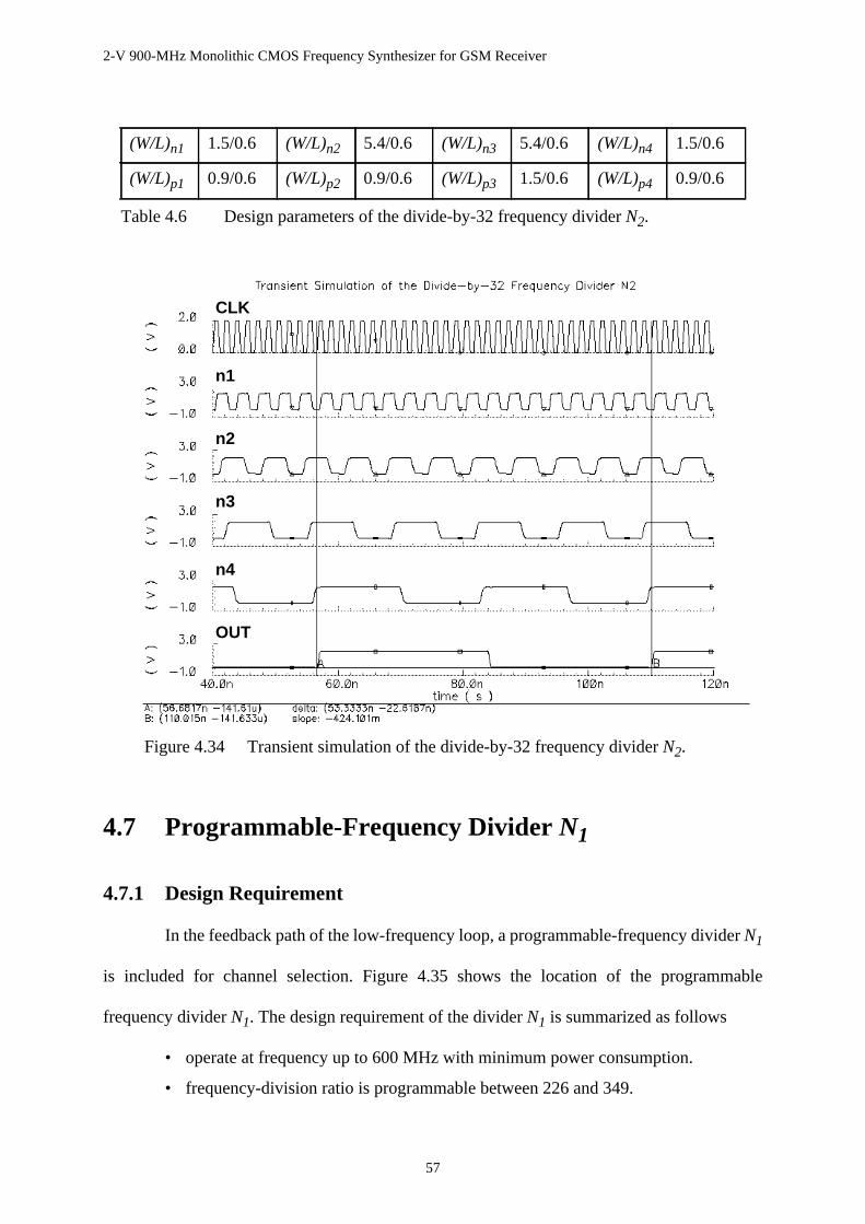
2-V 900-MHz Monolithic CMOS Frequency Synthesizer for GSM Receiver
57
4.7 Programmable-Frequency DividerN1
4.7.1 Design Requirement
In the feedback path of the low-frequency loop, a programmable-frequency dividerN1
is included for channel selection. Figure 4.35 shows the location of the programmable
frequency dividerN1. The design requirement of the dividerN1 is summarized as follows
• operate at frequency up to 600 MHz with minimum power consumption.
• frequency-division ratio is programmable between 226 and 349.
(W/L)n1 1.5/0.6 (W/L)n2 5.4/0.6 (W/L)n3 5.4/0.6 (W/L)n4 1.5/0.6
(W/L)p1 0.9/0.6 (W/L)p2 0.9/0.6 (W/L)p3 1.5/0.6 (W/L)p4 0.9/0.6
Table 4.6 Design parameters of the divide-by-32 frequency dividerN2.
n1
CLK
n2
n3
n4
OUT
Figure 4.34 Transient simulation of the divide-by-32 frequency dividerN2.

2-V 900-MHz Monolithic CMOS Frequency Synthesizer for GSM Receiver
58
• generate full-swing output with rise time and fall time less than 10% of the total
output period.
4.7.2 Circuit Implementation
The programmable-frequency dividerN1 shown in Figure 4.36 consists of a
dual-modulusN/N+1 prescaler, a program counter (P counter) and a swallow counter (S
counter) [18]. TheN/N+1 prescaler divides the input signal by eitherN or N+1. TheP counter,
fref2 = 205 MHz
fo = 865.2 ~ 889.8 MHz
2 = 32N
fin2 = 11.3 ~ 17.45 MHz
N = 2261
~ 349
fref1 /f in1 = 1.6 MHz
Programmable-Frequency Divider N 1
MixerLF1
3 = 4
LF2
High-Frequency Loop (HFL)
361.6 ~ 558.4 MHz
VCO1
Low
-Fre
quen
cy L
oop
(LF
L)
PFD1
PFD2
& CP1
& CP2
N
VCO2
Figure 4.35 Location of the programmable frequency dividerN1.
ModulusControl(Mode)
1 = (N + 1) S + N (P - S) = PN + SN
1/ N or N+1 1/P
1/S
Swallow Counter
Program CounterPrescaler
ResetOut
In Pre_in
Buffer
Figure 4.36 Implementation of the programmable-frequency dividerN1.
2-V 900-MHz Monolithic CMOS Frequency Synthesizer for GSM Receiver
59
which is itself a programmable frequency divider, divides the prescaler output byP. The S
counter, which is a programmable counter, counts the prescaler output byS.
When the programmable divider begins from the reset state, the prescaler divides input
signals byN+1. The prescaler output is counted by both theP counter and theS counter. When
S counter has countedS pulses, which is equivalent to(N+1)S input cycles, theS counter
changes the state of the modulus control lineMode and the prescaler divides input byN. Since
theP counter has already sensedS pulses, it counts the remainingP - S cycles, corresponding
to (P - S)N pulses at the main input, to reach overflow. Finally, the programmable divider
generates one complete cycle for every input cycles. The
operation repeats after theS counter is reset.
4.7.3 System-Design Optimization
As the frequency-division ratio (between 226 and 349) can be achieved with different
combinations ofN, S andP, different combinations have their own effect on the frequency
divider performance. Therefore, before the design optimization in transistor level, system
design optimization should be done. In this programmable-divider design, minimum power
consumption is the top criterion. The system design guidelines are shown as follows
• division ratio ofP counter must be larger than that ofS counter.
• minimize the operating frequency and number of bits for bothP andS counters.
The prescaler divides byN + 1 in the firstS cycles andN in the remainingP - S cycles. IfS is
larger thanP, S counter will be reset beforeS counter completes its counting and thus the divider
cannot function properly. Therefore,P must be larger thanS. In general, a programmable
counter is more power consuming than a non-programmable one. Therefore, operating
frequency and complexity of bothP andS counters should be minimized.
Table 4.7 shows different combinations ofN, P andS which can implement the desired
division ratio. In Case 1, it shows the highest operating frequency and the largest number of bits
N 1+( )S P S–( )N+ PN S+=
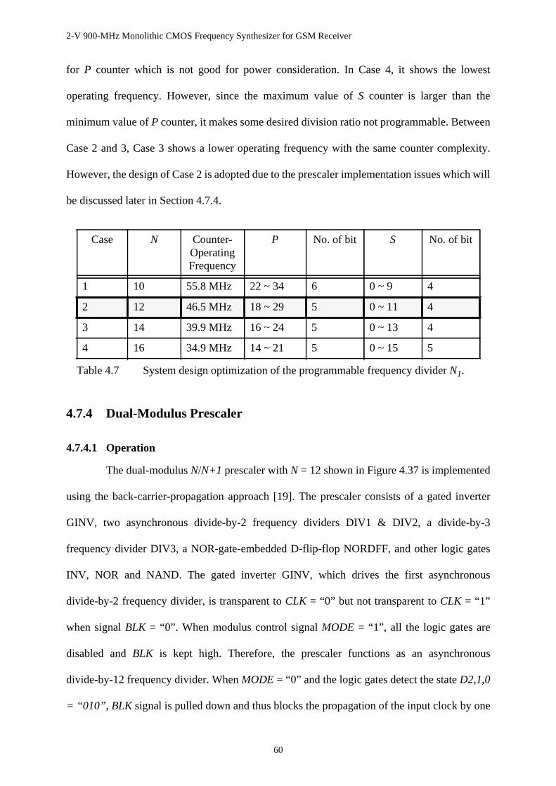
2-V 900-MHz Monolithic CMOS Frequency Synthesizer for GSM Receiver
60
for P counter which is not good for power consideration. In Case 4, it shows the lowest
operating frequency. However, since the maximum value ofS counter is larger than the
minimum value ofP counter, it makes some desired division ratio not programmable. Between
Case 2 and 3, Case 3 shows a lower operating frequency with the same counter complexity.
However, the design of Case 2 is adopted due to the prescaler implementation issues which will
be discussed later in Section 4.7.4.
4.7.4 Dual-Modulus Prescaler
4.7.4.1 Operation
The dual-modulusN/N+1 prescaler withN = 12 shown in Figure 4.37 is implemented
using the back-carrier-propagation approach [19]. The prescaler consists of a gated inverter
GINV, two asynchronous divide-by-2 frequency dividers DIV1 & DIV2, a divide-by-3
frequency divider DIV3, a NOR-gate-embedded D-flip-flop NORDFF, and other logic gates
INV, NOR and NAND. The gated inverter GINV, which drives the first asynchronous
divide-by-2 frequency divider, is transparent toCLK = “0” but not transparent toCLK = “1”
when signalBLK = “0”. When modulus control signalMODE = “1”, all the logic gates are
disabled andBLK is kept high. Therefore, the prescaler functions as an asynchronous
divide-by-12 frequency divider. WhenMODE = “0” and the logic gates detect the stateD2,1,0
= “010” , BLK signal is pulled down and thus blocks the propagation of the input clock by one
Case N Counter-OperatingFrequency
P No. of bit S No. of bit
1 10 55.8 MHz 22 ~ 34 6 0 ~ 9 4
2 12 46.5 MHz 18 ~ 29 5 0 ~ 11 4
3 14 39.9 MHz 16 ~ 24 5 0 ~ 13 4
4 16 34.9 MHz 14 ~ 21 5 0 ~ 15 5
Table 4.7 System design optimization of the programmable frequency dividerN1.

2-V 900-MHz Monolithic CMOS Frequency Synthesizer for GSM Receiver
61
cycle. With the one-period delay, the prescaler functions as a divide-by-13 frequency divider.
The advantage of back-carrier-propagation approach can be shown in Figure 4.38. The
asynchronous frequency divider counts from “101”, “001” to “010”. In each division period, the
higher order bitsD2 of the counter reach the final state “010” before the lower order bitD0.
Therefore, the earlier arriving information can be combined first and only quick detection ofD0
Mn1a
Mn1b
Mp1
D0 D1 D2/OUTDIV3DIV2DIV1
NORDFFNAND NOR
GINV
INV
DFF
MODE
CLK
BLK
Divide-by-2 Frequency Divider Divide-by-3 Frequency Divider
Figure 4.37 Circuit implementation of the dual-modulus prescaler:
CLK
D0
D1
D2
Final State "010"
Delay:
Delay:
Delay:
DIV1 & NORDFF
DIV2 & NAND
DIV3 & NOR
Figure 4.38 Relaxed timing requirement of the back-carrier-propagation approach.
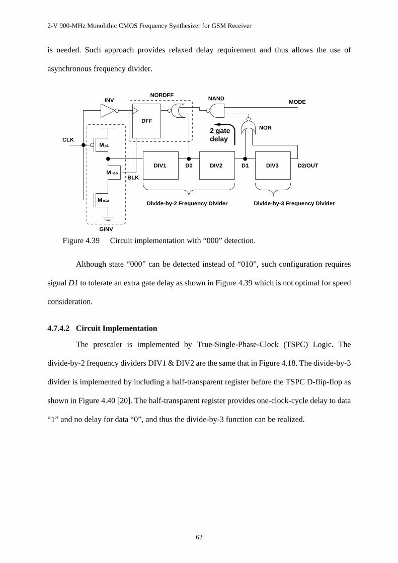
2-V 900-MHz Monolithic CMOS Frequency Synthesizer for GSM Receiver
62
is needed. Such approach provides relaxed delay requirement and thus allows the use of
asynchronous frequency divider.
Although state “000” can be detected instead of “010”, such configuration requires
signalD1 to tolerate an extra gate delay as shown in Figure 4.39 which is not optimal for speed
consideration.
4.7.4.2 Circuit Implementation
The prescaler is implemented by True-Single-Phase-Clock (TSPC) Logic. The
divide-by-2 frequency dividers DIV1 & DIV2 are the same that in Figure 4.18. The divide-by-3
divider is implemented by including a half-transparent register before the TSPC D-flip-flop as
shown in Figure 4.40 [20]. The half-transparent register provides one-clock-cycle delay to data
“1” and no delay for data “0”, and thus the divide-by-3 function can be realized.
Mn1a
Mn1b
Mp1
2 gatedelay
D0 D1 D2/OUTDIV3DIV2DIV1
NORDFFNAND
GINV
INV
DFF
CLK
BLK
Divide-by-2 Frequency Divider Divide-by-3 Frequency Divider
NOR
MODE
Figure 4.39 Circuit implementation with “000” detection.
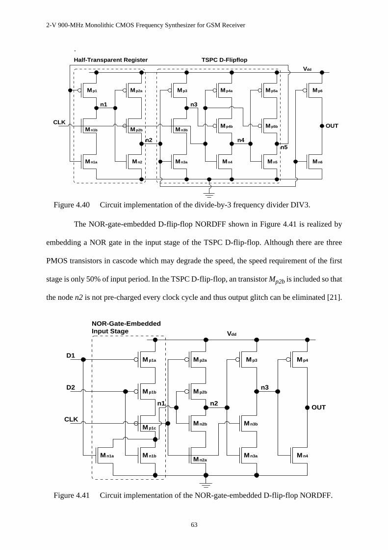
2-V 900-MHz Monolithic CMOS Frequency Synthesizer for GSM Receiver
63
.
The NOR-gate-embedded D-flip-flop NORDFF shown in Figure 4.41 is realized by
embedding a NOR gate in the input stage of the TSPC D-flip-flop. Although there are three
PMOS transistors in cascode which may degrade the speed, the speed requirement of the first
stage is only 50% of input period. In the TSPC D-flip-flop, an transistorMp2b is included so that
the noden2 is not pre-charged every clock cycle and thus output glitch can be eliminated [21].
p1M
n1bM
n1aM
p2aM
n2M
p2bM
p3M
n3bM
n3aM
p4aM
p4bM
n4M
p5aM
p5bM
n5M
p6M
n6M
Vdd
Half-Transparent Register TSPC D-Flipflop
CLK
n3
n4
OUT
n1
n2n5
Figure 4.40 Circuit implementation of the divide-by-3 frequency divider DIV3.
NOR-Gate-EmbeddedInput Stage Vdd
n1aM n1bM
p1aM
p1bM
p1cM
n2aM
n2bM
p2aM
p2bM
n3aM
n3bM
p3M
n4M
p4M
n1OUT
n3
n2
D1
D2
CLK
Figure 4.41 Circuit implementation of the NOR-gate-embedded D-flip-flop NORDFF.
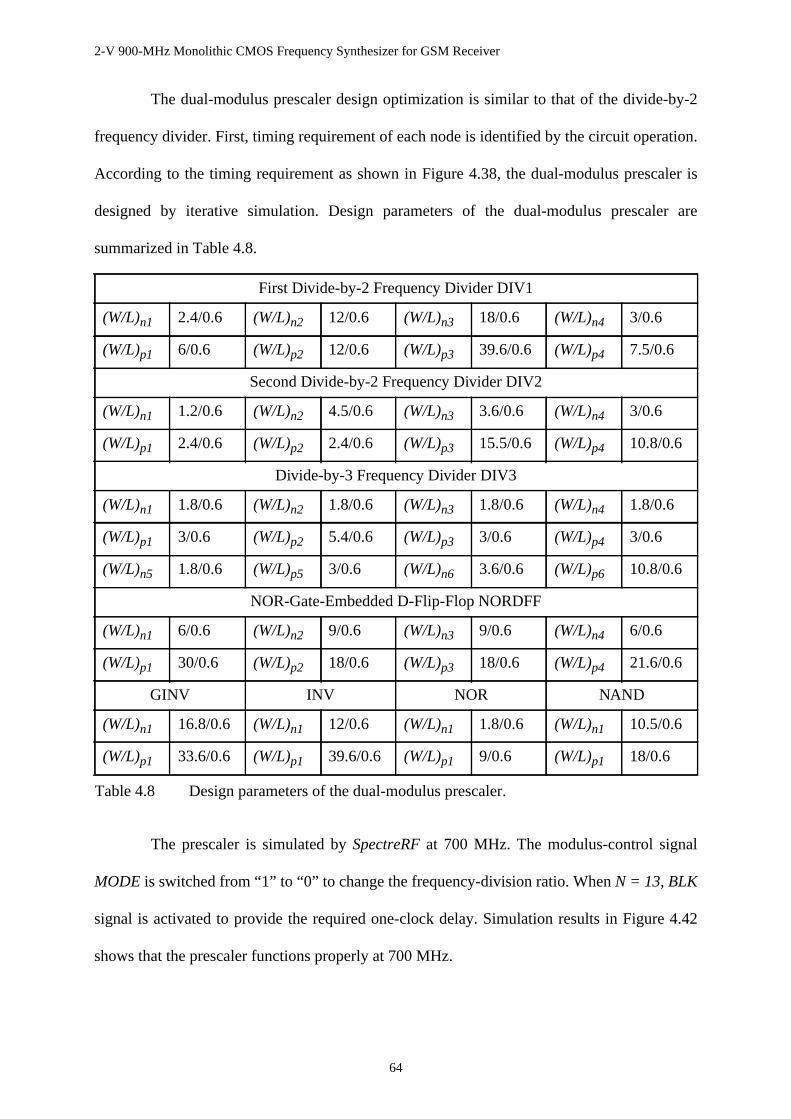
2-V 900-MHz Monolithic CMOS Frequency Synthesizer for GSM Receiver
64
The dual-modulus prescaler design optimization is similar to that of the divide-by-2
frequency divider. First, timing requirement of each node is identified by the circuit operation.
According to the timing requirement as shown in Figure 4.38, the dual-modulus prescaler is
designed by iterative simulation. Design parameters of the dual-modulus prescaler are
summarized in Table 4.8.
The prescaler is simulated bySpectreRF at 700 MHz. The modulus-control signal
MODE is switched from “1” to “0” to change the frequency-division ratio. WhenN = 13, BLK
signal is activated to provide the required one-clock delay. Simulation results in Figure 4.42
shows that the prescaler functions properly at 700 MHz.
First Divide-by-2 Frequency Divider DIV1
(W/L)n1 2.4/0.6 (W/L)n2 12/0.6 (W/L)n3 18/0.6 (W/L)n4 3/0.6
(W/L)p1 6/0.6 (W/L)p2 12/0.6 (W/L)p3 39.6/0.6 (W/L)p4 7.5/0.6
Second Divide-by-2 Frequency Divider DIV2
(W/L)n1 1.2/0.6 (W/L)n2 4.5/0.6 (W/L)n3 3.6/0.6 (W/L)n4 3/0.6
(W/L)p1 2.4/0.6 (W/L)p2 2.4/0.6 (W/L)p3 15.5/0.6 (W/L)p4 10.8/0.6
Divide-by-3 Frequency Divider DIV3
(W/L)n1 1.8/0.6 (W/L)n2 1.8/0.6 (W/L)n3 1.8/0.6 (W/L)n4 1.8/0.6
(W/L)p1 3/0.6 (W/L)p2 5.4/0.6 (W/L)p3 3/0.6 (W/L)p4 3/0.6
(W/L)n5 1.8/0.6 (W/L)p5 3/0.6 (W/L)n6 3.6/0.6 (W/L)p6 10.8/0.6
NOR-Gate-Embedded D-Flip-Flop NORDFF
(W/L)n1 6/0.6 (W/L)n2 9/0.6 (W/L)n3 9/0.6 (W/L)n4 6/0.6
(W/L)p1 30/0.6 (W/L)p2 18/0.6 (W/L)p3 18/0.6 (W/L)p4 21.6/0.6
GINV INV NOR NAND
(W/L)n1 16.8/0.6 (W/L)n1 12/0.6 (W/L)n1 1.8/0.6 (W/L)n1 10.5/0.6
(W/L)p1 33.6/0.6 (W/L)p1 39.6/0.6 (W/L)p1 9/0.6 (W/L)p1 18/0.6
Table 4.8 Design parameters of the dual-modulus prescaler.
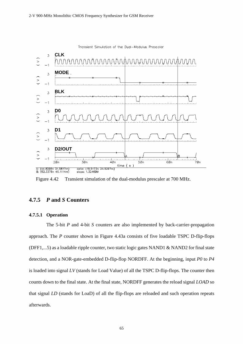
2-V 900-MHz Monolithic CMOS Frequency Synthesizer for GSM Receiver
65
4.7.5 P and S Counters
4.7.5.1 Operation
The 5-bitP and 4-bitS counters are also implemented by back-carrier-propagation
approach. TheP counter shown in Figure 4.43a consists of five loadable TSPC D-flip-flops
(DFF1,...5) as a loadable ripple counter, two static logic gates NAND1 & NAND2 for final state
detection, and a NOR-gate-embedded D-flip-flop NORDFF. At the beginning, inputP0 to P4
is loaded into signalLV (stands for Load Value) of all the TSPC D-flip-flops. The counter then
counts down to the final state. At the final state, NORDFF generates the reload signalLOAD so
that signalLD (stands for LoaD) of all the flip-flops are reloaded and such operation repeats
afterwards.
D0
D1
D2/OUT
BLK
MODE
CLK
Figure 4.42 Transient simulation of the dual-modulus prescaler at 700 MHz.
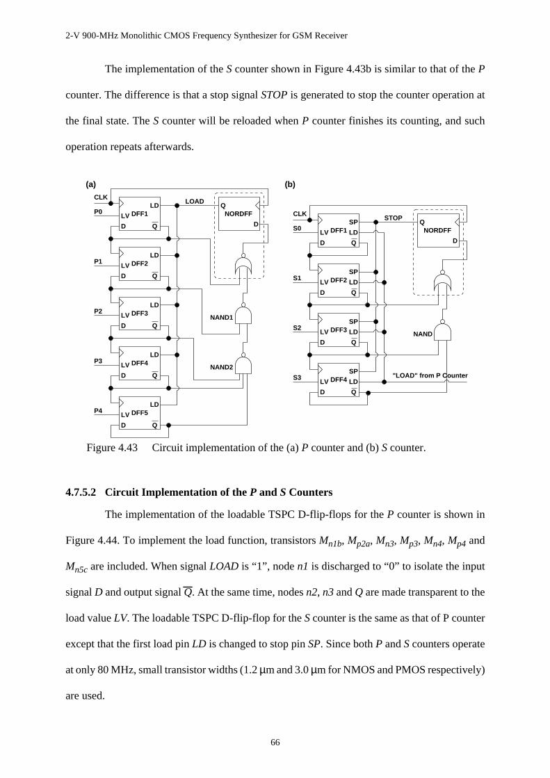
2-V 900-MHz Monolithic CMOS Frequency Synthesizer for GSM Receiver
66
The implementation of theS counter shown in Figure 4.43b is similar to that of theP
counter. The difference is that a stop signalSTOP is generated to stop the counter operation at
the final state. TheS counter will be reloaded whenP counter finishes its counting, and such
operation repeats afterwards.
4.7.5.2 Circuit Implementation of theP and S Counters
The implementation of the loadable TSPC D-flip-flops for theP counter is shown in
Figure 4.44. To implement the load function, transistorsMn1b, Mp2a, Mn3, Mp3, Mn4, Mp4 and
Mn5c are included. When signalLOAD is “1”, noden1 is discharged to “0” to isolate the input
signalD and output signalQ. At the same time, nodesn2, n3 andQ are made transparent to the
load valueLV. The loadable TSPC D-flip-flop for theS counter is the same as that of P counter
except that the first load pinLD is changed to stop pinSP. Since bothP andS counters operate
at only 80 MHz, small transistor widths (1.2µm and 3.0µm for NMOS and PMOS respectively)
are used.
D
QD
Q
(a) (b)
D
LV
Q
D
LV
Q
D
LV
Q
D
LV
Q
CLK
NORDFFDFF1
DFF2
DFF3
DFF4
SP
SP
SP
SP
LD
LD
LD
LD
S0
S1
S2
S3
STOPD
LV
Q
D
LV
Q
D
LV
Q
D
LV
Q
D
LV
Q
LD
LD
LD
LD
LDCLK
LOAD
P0
P1
P2
P3
P4
NORDFF
NAND1
NAND2
DFF1
DFF2
DFF3
DFF4
DFF5
"LOAD" from P Counter
NAND
Figure 4.43 Circuit implementation of the (a)P counter and (b)S counter.
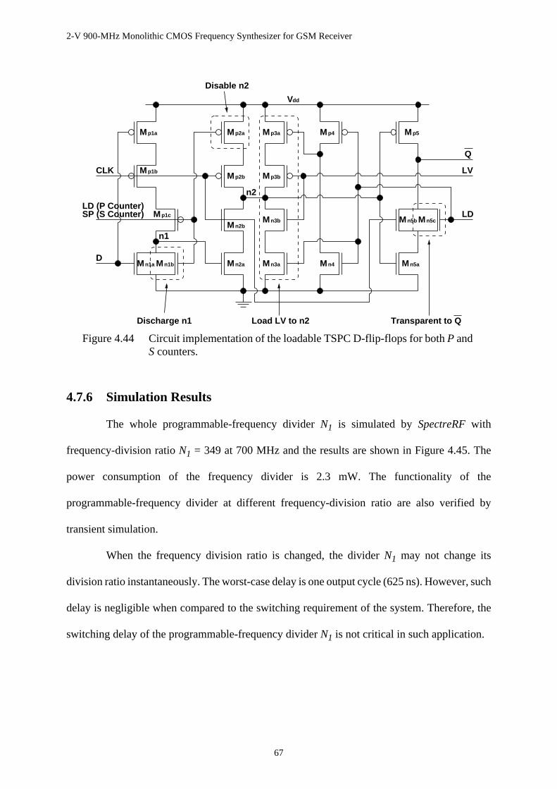
2-V 900-MHz Monolithic CMOS Frequency Synthesizer for GSM Receiver
67
4.7.6 Simulation Results
The whole programmable-frequency dividerN1 is simulated bySpectreRF with
frequency-division ratioN1 = 349 at 700 MHz and the results are shown in Figure 4.45. The
power consumption of the frequency divider is 2.3 mW. The functionality of the
programmable-frequency divider at different frequency-division ratio are also verified by
transient simulation.
When the frequency division ratio is changed, the dividerN1 may not change its
division ratio instantaneously. The worst-case delay is one output cycle (625 ns). However, such
delay is negligible when compared to the switching requirement of the system. Therefore, the
switching delay of the programmable-frequency dividerN1 is not critical in such application.
n1aM n1bM
p1aM
p1bM
p1cM
n2aM
n2bM
p2aM
p2bM
n3aM
n3bM
p3bM
p3aM
n4M
p4M p5M
n5aM
n5bM n5cM
ddV
Transparent to Q
n1
n2
Q
LV
LD
CLK
D
SP (S Counter)LD (P Counter)
Discharge n1 Load LV to n2
Disable n2
Figure 4.44 Circuit implementation of the loadable TSPC D-flip-flops for bothP andS counters.

2-V 900-MHz Monolithic CMOS Frequency Synthesizer for GSM Receiver
68
4.8 Phase-Frequency Detector PDF1 & PFD2
4.8.1 Design Requirement
Figure 4.46 shows the location of both PFD1 and PFD2. The PFDs compare the phases
between the reference input and the frequency-divider output and generates the corresponding
output signal to control the VCO frequencies. To simplify the design, the same PFD is used in
both low-frequency and high-frequency loops. The design requirement of the PFD is as follows
• operate at frequency up to 20 MHz.
• detect both phase and frequency error.
• eliminate dead-zone problem which limits the close-in phase-noise suppression.
Pre_in
RESET
OUT
Figure 4.45 Transient simulation of the programmable-frequency dividerN1 = 349.
Pre_in
OUT
RESET

2-V 900-MHz Monolithic CMOS Frequency Synthesizer for GSM Receiver
69
The origin of the dead zone in the PFD is the inability of digital logic gate to generate infinitely
short pulses. When phase error∆φ is very small, the PFD cannot compare phase error and the
PFD gainKPFD becomes zero as shown in Figure 4.47a. As the loop is broken, both reference
and VCO phase noise cannot be suppressed by the loop and thus close-in phase-noise is
significantly degraded as shown in Figure 4.47b [22].
4.8.2 Circuit Implementation
The implementation of the PFD is shown in Figure 4.48a. The PFD consists of two
TSPC half-transparent registers, a NAND gate and an inverter. As shown in Figure 4.48b, when
fref2 = 205 MHz
fo = 865.2 ~ 889.8 MHz
2 = 32N
fin2 = 11.3 ~ 17.45 MHz
N = 2261
~ 349
fref1 /f in1 = 1.6 MHz
MixerLF1
3 = 4
LF2
High-Frequency Loop (HFL)
361.6 ~ 558.4 MHz
VCO1
Low
-Fre
quen
cy L
oop
(LF
L)
N
PFD2& CP2
VCO2
PFD1&CP1
Figure 4.46 Location of the Phase-Frequency Detectors PFD1 & PFD2.
-2 π
2π
VOUT
(b)(a)
∆φ
VCO Spectrum
Dead Zone
Loop Bandwidth
f
With Dead Zone
Without Dead Zone
(Poorer Close-In Phase Noise)
Figure 4.47 The effect of (a) PFD transfer function and (b) close-in phase noise of the PFDwith/without dead zone.

2-V 900-MHz Monolithic CMOS Frequency Synthesizer for GSM Receiver
70
PFD inputIN1 has a rising edge first, aUP signal is generated to raise the oscillator frequency.
After certain time, PFD inputIN2 has a rising edge, aDOWN signal is generated to stop the
oscillator-frequency increment. Due to the delay of the NAND gate and inverter (Tdelay), both
UP andDOWN signals are turned on simultaneously for a period ofTdelay. The pulse width of
bothUP andDOWN signals are kept finite so that dead zone problem can be eliminated. After
Tdelay, a RESET signal is generated to reset both TSPC half-transparent registers. If the
frequency ofIN1 is larger than that ofIN2, the pulse width ofUP signal increases gradually so
that frequency difference can also be detected.
IN1
IN2
UP
DOWN
t
CLK
D
QHTDFF
D
CLK
QHTDFF
(a)
IN2
RESET
IN1UP
DOWN
Tdelay
(b)
Figure 4.48 PFD implementation: (a) block diagram and (b) operation.
n1M
p1aM
p1bM
n2aM
n2bM
p2M
n3M
p3M
n4M
p4M
n5M
p5M
ddV
Semi-Positive Feedback Stages
CLK
D
n2
n1
Q
Figure 4.49 Implementation of the TSPC half-transparent D-flip-flop of the PFDs.
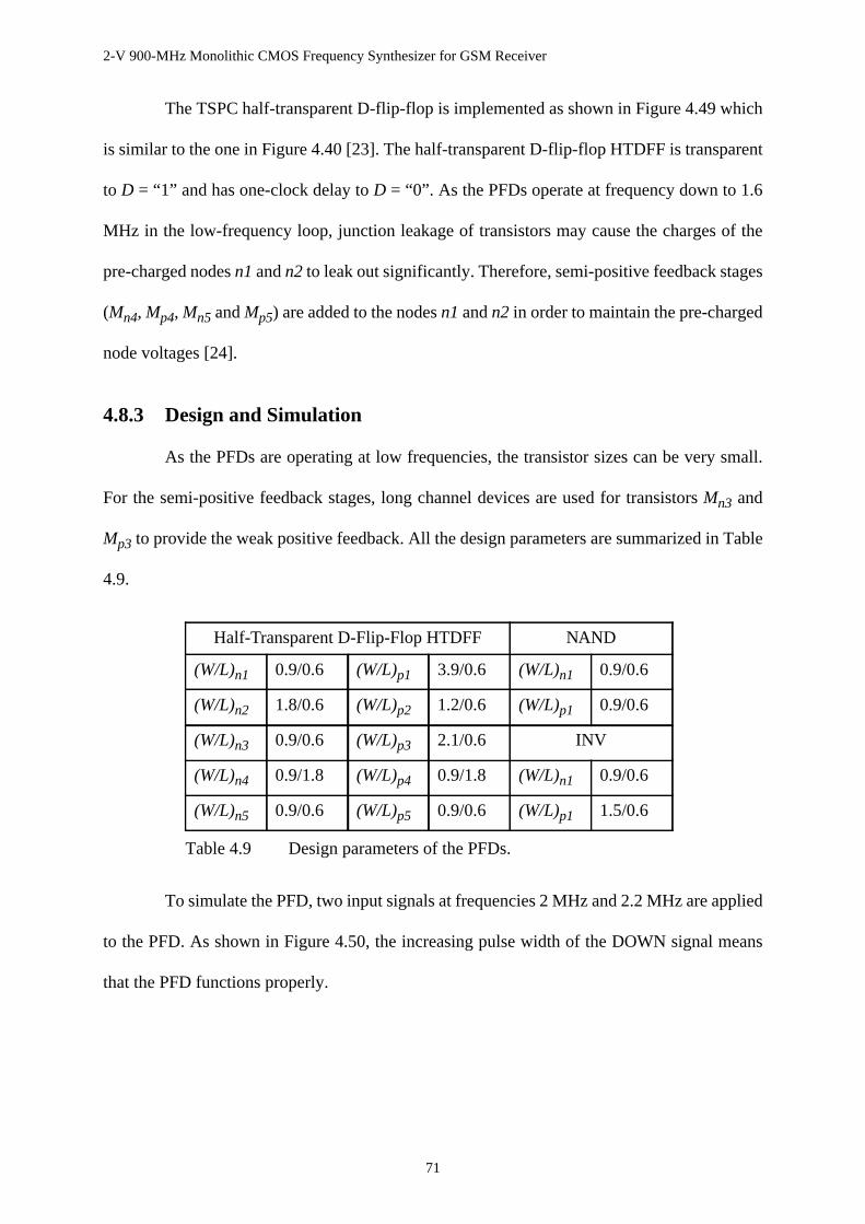
2-V 900-MHz Monolithic CMOS Frequency Synthesizer for GSM Receiver
71
The TSPC half-transparent D-flip-flop is implemented as shown in Figure 4.49 which
is similar to the one in Figure 4.40 [23]. The half-transparent D-flip-flop HTDFF is transparent
to D = “1” and has one-clock delay toD = “0”. As the PFDs operate at frequency down to 1.6
MHz in the low-frequency loop, junction leakage of transistors may cause the charges of the
pre-charged nodesn1 andn2 to leak out significantly. Therefore, semi-positive feedback stages
(Mn4, Mp4, Mn5 andMp5) are added to the nodesn1 andn2 in order to maintain the pre-charged
node voltages [24].
4.8.3 Design and Simulation
As the PFDs are operating at low frequencies, the transistor sizes can be very small.
For the semi-positive feedback stages, long channel devices are used for transistorsMn3 and
Mp3 to provide the weak positive feedback. All the design parameters are summarized in Table
4.9.
To simulate the PFD, two input signals at frequencies 2 MHz and 2.2 MHz are applied
to the PFD. As shown in Figure 4.50, the increasing pulse width of the DOWN signal means
that the PFD functions properly.
Half-Transparent D-Flip-Flop HTDFF NAND
(W/L)n1 0.9/0.6 (W/L)p1 3.9/0.6 (W/L)n1 0.9/0.6
(W/L)n2 1.8/0.6 (W/L)p2 1.2/0.6 (W/L)p1 0.9/0.6
(W/L)n3 0.9/0.6 (W/L)p3 2.1/0.6 INV
(W/L)n4 0.9/1.8 (W/L)p4 0.9/1.8 (W/L)n1 0.9/0.6
(W/L)n5 0.9/0.6 (W/L)p5 0.9/0.6 (W/L)p1 1.5/0.6
Table 4.9 Design parameters of the PFDs.

2-V 900-MHz Monolithic CMOS Frequency Synthesizer for GSM Receiver
72
4.9 Charge Pumps and Loop Filters
4.9.1 Design Requirement
Figure 4.51 shows the location of the charge pumps CP1 & CP2, and loop filters LF1
& LF2 of both loops. According to theUP andDOWN signals of the PFDs, charge pumps inject
or sink current to or from the loop filters. The loop filters filter out the high frequency
components, to maintain the spectral purity of the VCO. The design requirement of the
charge-pumps and loop filters are as follows
• operate at frequency up to 20 MHz.
• minimize the loop-filter chip area.
• satisfy the spurious-tone specification (< -88 dBc) and the phase-noise
specification (< -121 dBc/Hz@600kHz) of the frequency synthesizer.
To satisfy both the phase-noise and spurious-tone specification, the loop bandwidth of both
loops are reduced to several tens kHz. Therefore, large capacitors (~ 1 nF) and resistors (~ 100
kΩ) used for the loop-filter implementation are the very critical to the synthesizer integration.
IN1
IN2
UP
DOWN
Figure 4.50 Simulation results of the PFDs at 2 MHz.
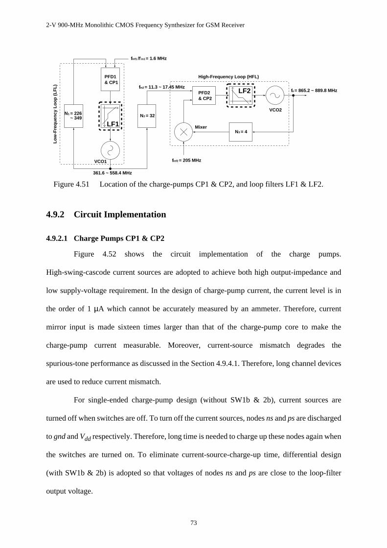
2-V 900-MHz Monolithic CMOS Frequency Synthesizer for GSM Receiver
73
4.9.2 Circuit Implementation
4.9.2.1 Charge Pumps CP1 & CP2
Figure 4.52 shows the circuit implementation of the charge pumps.
High-swing-cascode current sources are adopted to achieve both high output-impedance and
low supply-voltage requirement. In the design of charge-pump current, the current level is in
the order of 1µA which cannot be accurately measured by an ammeter. Therefore, current
mirror input is made sixteen times larger than that of the charge-pump core to make the
charge-pump current measurable. Moreover, current-source mismatch degrades the
spurious-tone performance as discussed in the Section 4.9.4.1. Therefore, long channel devices
are used to reduce current mismatch.
For single-ended charge-pump design (without SW1b & 2b), current sources are
turned off when switches are off. To turn off the current sources, nodesns andps are discharged
to gnd andVdd respectively. Therefore, long time is needed to charge up these nodes again when
the switches are turned on. To eliminate current-source-charge-up time, differential design
(with SW1b & 2b) is adopted so that voltages of nodesns andps are close to the loop-filter
output voltage.
fref2 = 205 MHz
fo = 865.2 ~ 889.8 MHz
2 = 32N
fin2 = 11.3 ~ 17.45 MHz
N = 2261
~ 349
fref1 /f in1 = 1.6 MHz
Mixer3 = 4
High-Frequency Loop (HFL)
361.6 ~ 558.4 MHz
VCO1
Low
-Fre
quen
cy L
oop
(LF
L)
PFD1
PFD2
& CP1
& CP2
N
VCO2
LF1
LF2
Figure 4.51 Location of the charge-pumps CP1 & CP2, and loop filters LF1 & LF2.

2-V 900-MHz Monolithic CMOS Frequency Synthesizer for GSM Receiver
74
As discussed in Section 4.9.4.2, complementary switches (SW1a, 1b, 2a & 2b) are used
to cancel out the clock feed through of the switches. Between nodesOUT andnb, an unity-gain
buffer UB is included to keep the voltages of nodesns, ps andnb to be the same as that of node
OUT. As discussed in Section 4.9.4.3, charge sharing between nodesns, ps andOUT can be
minimized with this buffer [25].
4.9.2.2 Loop-Filter Implementation LF1 & LF2
The loop filters of the frequency synthesizer are shown in Figure 4.53. It consists of a
IcpIcp
n1M p1M
SW1a
1bSW
2aSW2bSW
UP
DOWNddV
bn1aM
bn1bM
bn2aM
bn2bMbn2dM
bn2cM
bn3M
bp3M
bp2aM
bp2bM
bp1aM
bp1bM
ddV
Icp
DOWN
UP
ps
ns
nb VCOUB
UP
DOWN
116 ::2
16 12 : :
Current SourcesHigh-Swing Cascode
UP
DOWN
Figure 4.52 Circuit implementation of the charge pumps CP1 & CP2.
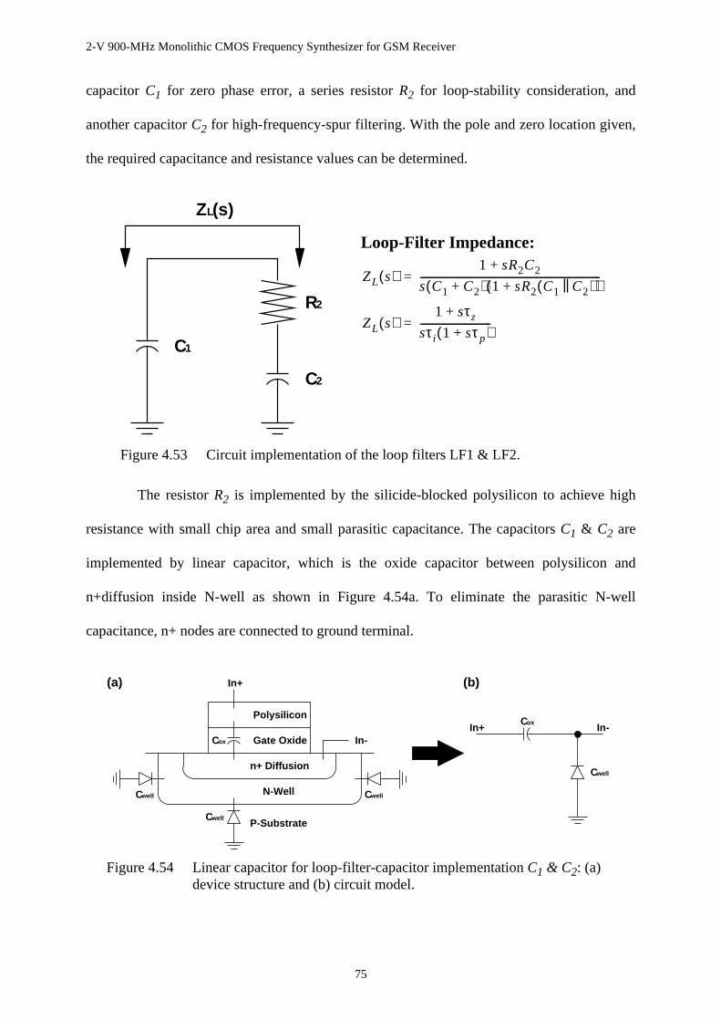
2-V 900-MHz Monolithic CMOS Frequency Synthesizer for GSM Receiver
75
capacitorC1 for zero phase error, a series resistorR2 for loop-stability consideration, and
another capacitorC2 for high-frequency-spur filtering. With the pole and zero location given,
the required capacitance and resistance values can be determined.
The resistorR2 is implemented by the silicide-blocked polysilicon to achieve high
resistance with small chip area and small parasitic capacitance. The capacitorsC1 & C2 are
implemented by linear capacitor, which is the oxide capacitor between polysilicon and
n+diffusion inside N-well as shown in Figure 4.54a. To eliminate the parasitic N-well
capacitance, n+ nodes are connected to ground terminal.
C1
R2
C2
ZL(s)
Figure 4.53 Circuit implementation of the loop filters LF1 & LF2.
ZL s( )1 sR2C2+
s C1 C2+( ) 1 sR2 C1 C2||( )+( )--------------------------------------------------------------------------=
ZL s( )1 sτz+
sτi 1 sτp+( )-----------------------------=
Loop-Filter Impedance:
Cox
Cwell
CwellCwell
Gate Oxide
Polysilicon
N-Well
n+ Diffusion
P-Substrate
In+
In-
Cwell
CoxIn+ In-
(a) (b)
Figure 4.54 Linear capacitor for loop-filter-capacitor implementationC1 & C2: (a)device structure and (b) circuit model.
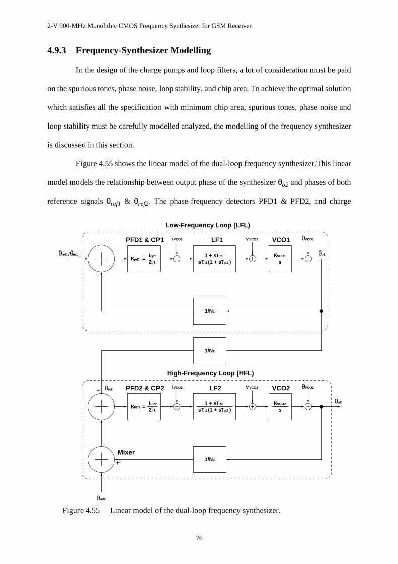
2-V 900-MHz Monolithic CMOS Frequency Synthesizer for GSM Receiver
76
4.9.3 Frequency-Synthesizer Modelling
In the design of the charge pumps and loop filters, a lot of consideration must be paid
on the spurious tones, phase noise, loop stability, and chip area. To achieve the optimal solution
which satisfies all the specification with minimum chip area, spurious tones, phase noise and
loop stability must be carefully modelled analyzed, the modelling of the frequency synthesizer
is discussed in this section.
Figure 4.55 shows the linear model of the dual-loop frequency synthesizer.This linear
model models the relationship between output phase of the synthesizerθo2 and phases of both
reference signalsθref1 & θref2. The phase-frequency detectors PFD1 & PFD2, and charge
1/N2
cp1I2πKpd1 =
sτ i1 (1 + sτp1 )1 + sτz1 KVCO1
s
1/N1
θref1 θin1/
VCO1θv VCO1iVCO1
θref2
1 + sτz2
sτ i2 (1 + sτp2 )KVCO2
s
1/N3
=KPD2ICP2
2πθo2
iVCO2 v VCO2 θVCO2
θo1
θin2
PFD1 & CP1 LF1 VCO1
Low-Frequency Loop (LFL)
Mixer
High-Frequency Loop (HFL)
PFD2 & CP2 LF2 VCO2
Figure 4.55 Linear model of the dual-loop frequency synthesizer.
2-V 900-MHz Monolithic CMOS Frequency Synthesizer for GSM Receiver
77
pumps CP1 & CP2 are modelled by subtractors which generate charge-pump currentICP
according to the phase difference. Although the phase-detector gainKPD shown in Figure 4.47
is non-linear, this model well models the linear characteristics of the PFDs. The loop filters are
modelled by an integratorτi for zero phase error, a zeroτz for stability consideration and another
poleτp for high-frequency-spur filtering. For the voltage-controlled oscillators VCO1 & VCO2,
output frequencyfo is proportional to the VCO-control voltagevVCO. Therefore, the VCO,
which is the transfer function between control voltagevVCO to output phaseθo2, is modelled by
the product of an integrator and VCO gainKVCO. As frequency division is the same as phase
division, frequency dividersN1, N2 and N3 are modelled by gain factors1/N1, 1/N2 and1/N3
respectively. Since down-conversion mixing produces frequency substraction as well as phase
subtraction, the down-conversion mixer is modelled by a subtractor.
Based on the linear model of the frequency synthesizer, transfer function from input
phaseθin to output phaseθo of both low-frequency and high-frequency loops can be expressed
as follows
(4.15)
whereKPD is phase-detector gain,KVCO is VCO gain,τi is integrator time constant,τz is zero
time constant, andτp is pole time constant. For the spurious-tone analysis in Section 4.9.4, the
transfer functions from charge-pump currentiCP to output phaseθo can be expressed as follows
(4.16)
θo1
θin1--------- s( )
N1 1 sτz1+( )
1 sτz1 N1τi1 KPD1KVCO1⁄( )s21 sτp11
+( )+ +--------------------------------------------------------------------------------------------------------------=
θo2
θin2--------- s( )
N3 1 sτz2+( )
1 sτz2 N3τi2 KPD2KVCO2⁄( )s21 sτp21
+( )+ +--------------------------------------------------------------------------------------------------------------=
θo1
iCP1---------- s( )
N1 KPD1⁄( ) 1 sτz1+( )
1 sτz1 N1τi1 KPD1KVCO1⁄( )s21 sτp11
+( )+ +--------------------------------------------------------------------------------------------------------------=
θo2
iCP2---------- s( )
N3 KPD2⁄( ) 1 sτz2+( )
1 sτz2 N3τi2 KPD2KVCO2⁄( )s21 sτp21
+( )+ +--------------------------------------------------------------------------------------------------------------=

2-V 900-MHz Monolithic CMOS Frequency Synthesizer for GSM Receiver
78
For the phase-noise analysis of charge pumps and loop filters in Section 4.9.5.1, the transfer
functions from VCO-control voltagevVCO to output phaseθo can be expressed as follows
(4.17)
For the phase-noise analysis of VCOs in Section 4.9.5.2, the transfer functions from
VCO-output phaseθVCO to output phaseθo can be expressed as follows
(4.18)
4.9.4 Spurious-Tone Analysis
In this section, the spurious tones, which is mainly caused by the charge pumps, is
discussed. Different causes of the spurious tones such as current mismatch, clock feed through,
charge injection, and charge sharing are discussed and analyzed. Based on the analysis results,
the charge pumps are designed accordingly to optimize the spurious-tone performance.
4.9.4.1 Current Mismatch
As discussed in Section 4.8.2, a feedback-delay timeTdelay is added in the PFDs in
order to eliminate the dead-zone problem. During the delay time, both pull-up and pull-down
charge-pump current are turned on. In the ideal situation, these pull-up and pull-down current
are exactly the same so that no net current is injected into the loop filter. However, the mismatch
between pull-up and pull-down charge-pump current introduces current injection∆ICP as
shown in Figure 4.56. Such current disturbs the nodeVCO and causes spurious tones.
θo1
vVCO1-------------- s( )
N1 KVCO1⁄( )s 1 sτp1+( )
1 sτz1 N1τi1 KPD1KVCO1⁄( )s21 sτp11
+( )+ +--------------------------------------------------------------------------------------------------------------=
θo2
vVCO2-------------- s( )
N3 KVCO2⁄( )s 1 sτp2+( )
1 sτz2 N3τi2 KPD2KVCO2⁄( )s21 sτp21
+( )+ +--------------------------------------------------------------------------------------------------------------=
θo1
θVCO1--------------- s( )
N1 KPD1KVCO1⁄( )s21 sτp1+( )
1 sτz1 N1τi1 K pd1KVCO1⁄( )s21 sτp11
+( )+ +-------------------------------------------------------------------------------------------------------------=
θo2
θVCO2--------------- s( )
N3 KPD2KVCO2⁄( )s21 sτp2+( )
1 sτz2 N3τi2 K pd2KVCO2⁄( )s21 sτp21
+( )+ +-------------------------------------------------------------------------------------------------------------=

2-V 900-MHz Monolithic CMOS Frequency Synthesizer for GSM Receiver
79
The cause of the current mismatch is mainly due to the mismatches of channel width
W, channel lengthL, and threshold voltageVt of current mirrors as shown in Figure 4.57.
Assume that cascode transistors do not have any effect in the mismatch, the current mismatch
of a current mirror can be expressed as follows
(4.19)
cpI
∆IcpcpI +
1C
C 2
R 2
Tdelay
Icp (t)
∆Icp
|Icp (f)|2
1/Tdelay
Spurious Tone
UP
DOWN
t
Tin
f1/Tin
Figure 4.56 Charge-pump current-injection mismatch: (a) cause, (b) transientresponse, and (c) frequency response.
IcpIcp
ddV
Icp +∆Icp
W/L
W/L
W/L
Cascode Devices
Figure 4.57 Current-mismatch analysis of a current mirror.
∆II
------ ∆WW
--------- ∆LL
-------2Vt
Vgs Vt–--------------------
∆Vt
Vt---------
+ +=

2-V 900-MHz Monolithic CMOS Frequency Synthesizer for GSM Receiver
80
To reduce the current mismatch, wide and long channel devices (L = 3 µm) are used.
Although Vgs - Vt should be increased to reduce current mismatch due to threshold-voltage
mismatch, it reduce the output range of the charge pump. Therefore,Vgs - Vt is designed to be
0.2 V to compromise these two design criteria.
The total charge-pump current mismatch is caused by the mismatches between the
NMOS and PMOS current mirrors in Figure 4.52. Based on the same disturbance analysis, the
total charge-pump current mismatch can be expressed as follows
(4.20)
Assume the charge-pump current waveform is the same as that in Figure 4.56b, the
spurious-tone performance due to the charge-pump current mismatch of both loopsSCM_CP1&
SCM_CP2 can be expressed as follows
(4.21)
whereSCM_CP1 ωin1 and SCM_CP2 ωin2 are the spurious-tone performance of charge pump
current mismatch of the low-frequency loop and high-frequency loop respectively,∆ICP1 &
∆ICP2 are charge-pump current mismatch of the low-frequency and high-frequency loops
respectively,Tdelay1 & Tdelay2 are feedback-delay time of PFDs of both loops, andTin1 & Tin2
are input periods of both loops.
To improve spurious-tone performance, charge-pump current mismatch should be
reduced according to (4.20). Since the spur power is proportional to current-injection time,
∆I CP
I CP------------
∆Wbn1
Wbn1----------------
∆Lbn1
Lbn1--------------
2Vtbn1
Vgsbn1 Vtbn1–-----------------------------------
∆Vtbn1
Vtbn1-----------------
+ +=
∆Wbp1
Wbp1----------------
∆Lbp1
Lbp1--------------
2Vtbp1
Vgsbp1 Vtbp1–-----------------------------------
∆Vtbp1
Vtb1-----------------
+ + +
SCM_CP1 ωin1 12---
2∆I CP1
π------------------
2 πTdelay1
Tin1---------------------
2sin
θo1
iCP1---------- ωin1( )
2 1N2------
2 θo2
θin2--------- ωin1( )
2⋅ ⋅ ⋅ ⋅=
SCM_CP2 ωin2 12---
2∆I CP2
π------------------
2 πTdelay2
Tin2---------------------
2sin
θo2
iCP2---------- ωin2( )
2⋅ ⋅=
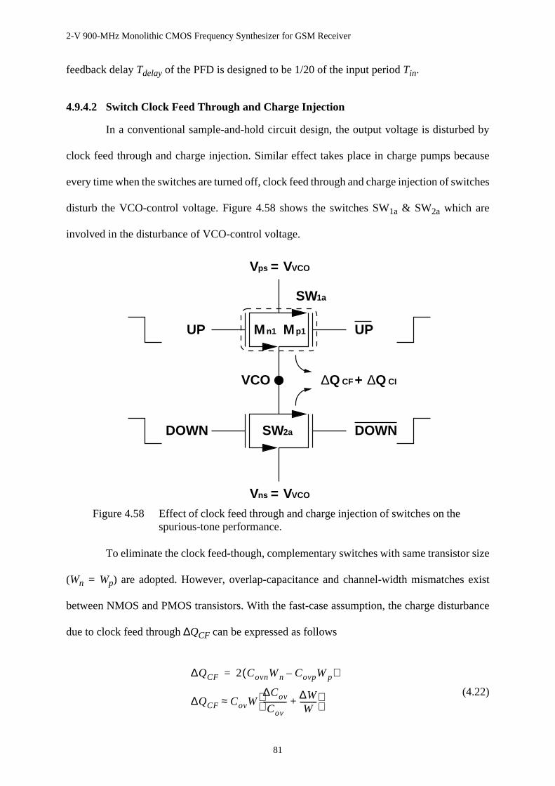
2-V 900-MHz Monolithic CMOS Frequency Synthesizer for GSM Receiver
81
feedback delayTdelay of the PFD is designed to be 1/20 of the input periodTin.
4.9.4.2 Switch Clock Feed Through and Charge Injection
In a conventional sample-and-hold circuit design, the output voltage is disturbed by
clock feed through and charge injection. Similar effect takes place in charge pumps because
every time when the switches are turned off, clock feed through and charge injection of switches
disturb the VCO-control voltage. Figure 4.58 shows the switches SW1a & SW2a which are
involved in the disturbance of VCO-control voltage.
To eliminate the clock feed-though, complementary switches with same transistor size
(Wn = Wp) are adopted. However, overlap-capacitance and channel-width mismatches exist
between NMOS and PMOS transistors. With the fast-case assumption, the charge disturbance
due to clock feed through∆QCF can be expressed as follows
(4.22)
2aSW
SW1a
DOWN
n1M p1M
Vps
Vns
UPUP
= VVCO
= VVCO
DOWN
Q∆ CI+CFQ∆VCO
Figure 4.58 Effect of clock feed through and charge injection of switches on thespurious-tone performance.
∆QCF 2 CovnWn CovpWp–( )=
∆QCF CovW∆Cov
Cov------------ ∆W
W---------+
≈
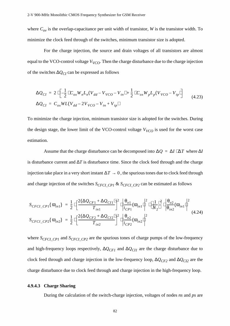
2-V 900-MHz Monolithic CMOS Frequency Synthesizer for GSM Receiver
82
whereCov is the overlap-capacitance per unit width of transistor,W is the transistor width. To
minimize the clock feed through of the switches, minimum transistor size is adopted.
For the charge injection, the source and drain voltages of all transistors are almost
equal to the VCO-control voltageVVCO. Then the charge disturbance due to the charge injection
of the switches∆QCI can be expressed as follows
(4.23)
To minimize the charge injection, minimum transistor size is adopted for the switches. During
the design stage, the lower limit of the VCO-control voltageVVCO is used for the worst case
estimation.
Assume that the charge disturbance can be decomposed into where∆I
is disturbance current and∆T is disturbance time. Since the clock feed through and the charge
injection take place in a very short instant , the spurious tones due to clock feed through
and charge injection of the switchesSCFCI_CP1 & SCFCI_CP2 can be estimated as follows
(4.24)
whereSCFCI_CP1 andSCFCI_CP2 are the spurious tones of charge pumps of the low-frequency
and high-frequency loops respectively,∆QCF1 and∆QCI1 are the charge disturbance due to
clock feed through and charge injection in the low-frequency loop,∆QCF2 and∆QCI2 are the
charge disturbance due to clock feed through and charge injection in the high-frequency loop.
4.9.4.3 Charge Sharing
During the calculation of the switch-charge injection, voltages of nodesns andps are
∆QCI 2 12---– CoxWnLn Vdd VVCO– Vtn–( ) 1
2--- CoxWpLp VVCO Vtp–( )⋅+⋅⋅=
∆QCI CoxWL Vdd 2VVCO– Vtn– Vtp+( )=
∆Q ∆I ∆T⋅=
∆T 0→
SCFCI_CP1 ωin1 12---
2 ∆QCF1 ∆QCI1+( )Tin1
-----------------------------------------------2 θo1
iCP1---------- ωin1( )
2 1N2------
2 θo2
θin2--------- ωin1( )
2⋅ ⋅ ⋅ ⋅=
SCFCI_CP2 ωin2 12---
2 ∆QCF2 ∆QCI2+( )Tin2
-----------------------------------------------2 θo2
iCP2---------- ωin2( )
2⋅ ⋅=
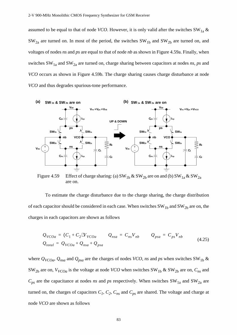
2-V 900-MHz Monolithic CMOS Frequency Synthesizer for GSM Receiver
83
assumed to be equal to that of nodeVCO. However, it is only valid after the switches SW1a &
SW2a are turned on. In most of the period, the switches SW1b and SW2b are turned on, and
voltages of nodesns andps are equal to that of nodenb as shown in Figure 4.59a. Finally, when
switches SW1a and SW2a are turned on, charge sharing between capacitors at nodesns, ps and
VCO occurs as shown in Figure 4.59b. The charge sharing causes charge disturbance at node
VCO and thus degrades spurious-tone performance.
To estimate the charge disturbance due to the charge sharing, the charge distribution
of each capacitor should be considered in each case. When switches SW1b and SW2b are on, the
charges in each capacitors are shown as follows
(4.25)
whereQVCOa, Qnsa andQpsa are the charges of nodesVCO, ns andps when switches SW1b &
SW2b are on,VVCOa is the voltage at nodeVCO when switches SW1b & SW2b are on,Cns and
Cps are the capacitance at nodesns andps respectively. When switches SW1a and SW2a are
turned on, the charges of capacitorsC1, C2, Cns andCps are shared. The voltage and charge at
nodeVCO are shown as follows
Icp
Icp
Vnb
Vdd
Cps
Cns
C1
C2
R2
SW1aSW1b
SW2aSW2b
Vns Vps= =VVCO
1aSW 2aSW& are on
nb VCO
ns
ps
(b)
Icp
Icp
Vnb
Vdd
Cps
Cns
C1
C2
R2
Vns Vps Vnb= =
SW1aSW1b
SW2aSW2b
1bSW 2bSW& are on
nb VCO
ns
ps
(a)
UP & DOWN
Figure 4.59 Effect of charge sharing: (a) SW1b & SW2b are on and (b) SW1a & SW2aare on.
QVCOa C1 C2+( )VVCOa= Qnsa CnsVnb= Qpsa CpsVnb=
Qtotal QVCOa Qnsa Qpsa+ +=

2-V 900-MHz Monolithic CMOS Frequency Synthesizer for GSM Receiver
84
(4.26)
whereVVCOb andQVCOb are the voltage and charge at theVCO node respectively after switches
SW1a & SW2a are turned on. Based on the charges of theVCO node in these two cases, the
charge disturbance due to charge sharing∆QCS can be expressed as follows
(4.27)
where∆QCS is the charge disturbance of nodeVCO due to charge sharing,VVCO_ERR is the
voltage difference between nodesVCO andnb. Similar to the analysis of clock feed through and
charge injection of the switches, the spurious tones of the charge pumps of the low-frequency
and high-frequency loops can be expressed as follows
(4.28)
whereSCS_CP1 andSCS_CP2 are the spurious tones due to charge sharing of the low-frequency
and high-frequency loops respectively,∆QCS1 and∆QCS2 are the charge disturbance due to
charge charging of the low-frequency and high-frequency loops respectively.
To minimize the spurious tones due to charge sharing, capacitanceCns andCp2 should
be minimized in the layout. The most effective method to solve this charge-sharing problem is
to keep the voltages of nodesVCO andnb to be the same. Therefore, an unity-gain buffer UB
is included between nodesVCO andnb as shown in Figure 4.52.
VVCOb
C1 C2+( )VVCOa Cns Cps+( )+ Vnb
C1 C2 Cns Cps+ + +-------------------------------------------------------------------------------------=
QVCOb C1 C2+( )VVCOb=
∆QCS C1 C2+( ) VVCOb VVCOa–( )=
∆QCS
C1 C2+( ) Cns Cps+( )C1 C2 Cns Cps+ + +
----------------------------------------------------- VVCOa Vnb–( )=
∆QCS
C1 C2+( ) Cns Cps+( )C1 C2 Cns Cps+ + +
-----------------------------------------------------VVCO_ERR=
SCS_CP1 ωin1 12---
2∆QCS1
Tin1--------------------
2 θo1
iCP1---------- ωin1( )
2 1N2------
2 θo2
θin2--------- ωin1( )
2⋅ ⋅ ⋅ ⋅=
SCS_CP2 ωin2 12---
2∆QCS2
Tin2--------------------
2 θo2
iCP2---------- ωin2( )
2⋅ ⋅=
2-V 900-MHz Monolithic CMOS Frequency Synthesizer for GSM Receiver
85
4.9.4.4 Total Spurious-Tone Performance
In the previous sections, the spurious tones due to the current mismatch, clock feed
through, charge injection and charge sharing are discussed and analyzed. Assume that all the
spurious tones have the same phase for the worst case estimation, the total spurious tones of the
charge pumps of the low-frequency and high-frequency loops can be expressed as follows
(4.29)
4.9.4.5 Spurious-Tone Optimization
To improve the spurious-tone performance, the design guidelines are as follows
• use long-channel devices for the current sources to reduce current mismatch
• use minimum-size transistors for the switches to reduce clock feed through and
charge injection.
• minimize the capacitance at nodesns andps to suppress charge-sharing effect.
• use an unity-gain buffer to keep voltages between nodesVCO andnb to be equal.
• reduce loop bandwidth to improve spurious-tone suppression.
The first four criteria are for the charge-pump design which can be achieved easily. However,
the loop-bandwidth reduction increases the required loop-filter chip area. The loop-bandwidth
design optimization will be discussed in Section 4.9.7.
4.9.5 Phase-Noise Analysis
In this section, phase noise of the dual-loop frequency synthesizer is discussed. For the
reference signals and frequency dividers, their phase noise is very low. Therefore, the
phase-noise discussion is focused on the charge pumps, loop filters and VCOs. The phase-noise
analysis is similar to that of the spurious tones. First noise voltage of the node VCO is
calculated, and phase noise can then be obtained by the VCO-voltage-to-output-phase transfer
function in (4.17).
SCP1 ωin1 SCM_CP12 ωin1 SCFCI_CP1
2 ωin1 SCS_CP12 ωin1 + +=
SCP2 ωin2 SCM_CP22 ωin2 SCFCI_CP2
2 ωin2 SCS_CP22 ωin2 + +=
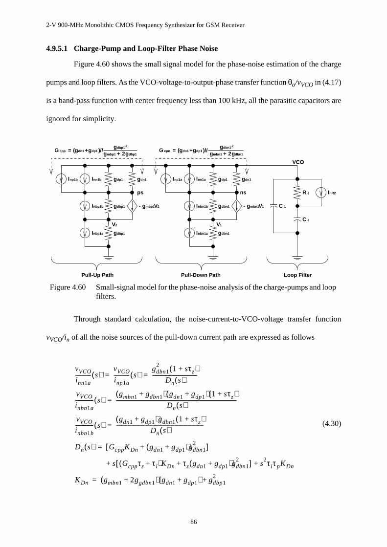
2-V 900-MHz Monolithic CMOS Frequency Synthesizer for GSM Receiver
86
4.9.5.1 Charge-Pump and Loop-Filter Phase Noise
Figure 4.60 shows the small signal model for the phase-noise estimation of the charge
pumps and loop filters. As the VCO-voltage-to-output-phase transfer functionθo/vVCO in (4.17)
is a band-pass function with center frequency less than 100 kHz, all the parasitic capacitors are
ignored for simplicity.
Through standard calculation, the noise-current-to-VCO-voltage transfer function
vVCO/in of all the noise sources of the pull-down current path are expressed as follows
(4.30)
mbp1g- V2
2V
nbp1bI
nbp1aI
np1bI nn1bI dn1gdp1g
g
dbp1g
dn1g dp1gcppGdbp1g
gmbp1 dbp1g( + )= //
+ 2
2
ps
dbp1
1V
nbn1bI
nbn1aI
dbn1g
dp1g dn1g
mbn1g- V1
dbn1g
dn1g dp1ggmbn1 dbn1g
dbn1gcpn =G ( + )//
+ 2
2
ns
np1aI nn1aI
1C
2C
2R nR2I
VCO
Loop FilterPull-Down PathPull-Up Path
Figure 4.60 Small-signal model for the phase-noise analysis of the charge-pumps and loopfilters.
vVCO
inn1a------------ s( )
vVCO
inp1a------------ s( )
gdbn12
1 sτz+( )Dn s( )
----------------------------------= =
vVCO
inbn1a-------------- s( )
gmbn1 gdbn1+( ) gdn1 gdp1+( ) 1 sτz+( )Dn s( )
--------------------------------------------------------------------------------------------=
vVCO
inbn1b-------------- s( )
gdn1 gdp1+( )gdbn1 1 sτz+( )Dn s( )
-------------------------------------------------------------------=
Dn s( ) GcppKDn gdn1 gdp1+( )gdbn12
+[ ]=
s Gcppτz τi+( )KDn τz gdn1 gdp1+( )gdbn12
+[ ] s2τiτpKDn+ +
KDn gmbn1 2ggdbn1+( ) gdn1 gdp1+( ) gdbp12
+=
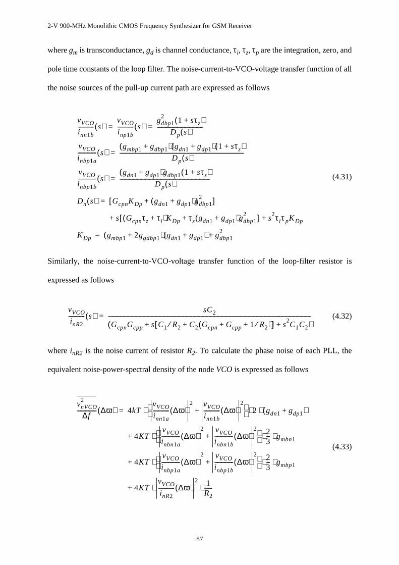
2-V 900-MHz Monolithic CMOS Frequency Synthesizer for GSM Receiver
87
wheregm is transconductance,gd is channel conductance,τi, τz, τp are the integration, zero, and
pole time constants of the loop filter. The noise-current-to-VCO-voltage transfer function of all
the noise sources of the pull-up current path are expressed as follows
(4.31)
Similarly, the noise-current-to-VCO-voltage transfer function of the loop-filter resistor is
expressed as follows
(4.32)
whereinR2 is the noise current of resistorR2. To calculate the phase noise of each PLL, the
equivalent noise-power-spectral density of the nodeVCO is expressed as follows
(4.33)
vVCO
inn1b------------ s( )
vVCO
inp1b------------ s( )
gdbp12
1 sτz+( )Dp s( )
----------------------------------= =
vVCO
inbp1a-------------- s( )
gmbp1 gdbp1+( ) gdn1 gdp1+( ) 1 sτz+( )Dp s( )
--------------------------------------------------------------------------------------------=
vVCO
inbp1b-------------- s( )
gdn1 gdp1+( )gdbp1 1 sτz+( )Dp s( )
-------------------------------------------------------------------=
Dn s( ) GcpnKDp gdn1 gdp1+( )gdbp12
+[ ]=
s Gcpnτz τi+( )KDp τz gdn1 gdp1+( )gdbp12
+[ ] s2τiτpKDp+ +
KDp gmbp1 2ggdbp1+( ) gdn1 gdp1+( ) gdbp12
+=
vVCO
inR2------------ s( )
sC2
GcpnGcpp s C1 R2⁄ C2 Gcpn Gcpp 1 R2⁄+ +( )+[ ] s2C1C2+ +( )
-------------------------------------------------------------------------------------------------------------------------------------------------------=
vnVCO2
∆f-------------- ∆ω( ) 4kT
vVCO
inn1a------------ ∆ω( )
2 vVCO
inn1b------------ ∆ω( )
2+
2 gdn1 gdp1+( )⋅ ⋅⋅=
4KTvVCO
inbn1a-------------- ∆ω( )
2 vVCO
inbn1b-------------- ∆ω( )
2+
23--- gmbn1⋅ ⋅ ⋅+
4KTvVCO
inbp1a-------------- ∆ω( )
2 vVCO
inbp1b-------------- ∆ω( )
2+
23--- gmbp1⋅ ⋅ ⋅+
4KTvVCO
inR2------------ ∆ω( )
2 1R2------⋅ ⋅+
2-V 900-MHz Monolithic CMOS Frequency Synthesizer for GSM Receiver
88
where is the noise power-spectral density of nodeVCO due to charge pump and loop
filter, ∆ω is the offset frequency in radian per second.
From the previous phase-noise equations, the phase-noise performance of the
dual-loop frequency synthesizer due to the charge pumps and loop filters of the low-frequency
and high frequency loops are expressed as follows
(4.34)
whereLCP1 ∆ω and LCP2 ∆ω are phase noise due to charge pumps and loop filters of the
low-frequency and high-frequency loops respectively, and are the
noise power-spectral density at nodesVCO1 andVCO2 due to charge-pumps and loop filters of
the low-frequency and high-frequency loops respectively.
4.9.5.2 Voltage-Controlled Oscillator Phase Noise
In Section 4.2.6 and Section 4.5.4, the phase noise at 600-kHz frequency offset of the
LC and ring oscillators are simulated bySpectreRF. In general, the phase noise is inversely
proportional to the square of offset frequency, the phase noise of both oscillators are expressed
as follows
(4.35)
whereLVCO1 ∆ω andLVCO2 ∆ω are the phase noise of the oscillatorsVCO1 andVCO2, ∆ω
is the offset frequency.
vnVCO2 ∆f⁄
LTotal_CP1 ∆ω θo1
vVCO1-------------- ∆ω( )
2 1N2------
2 θo2
θin2--------- ∆ω( )
2 vnVCO12
∆f-----------------⋅ ⋅ ⋅=
LTotal_CP2 ∆ω θo2
vVCO2-------------- ∆ω( )
2 vnVCO22
∆f-----------------⋅=
vnVCO12 ∆f⁄ vnVCO2
2 ∆f⁄
LVCO1 ∆ω 10112 10⁄–
2π 6003×10×( )
2
∆ω2----------------------------------------------------------------=
LVCO2 ∆ω 10124 10⁄–
2π 6003×10×( )
2
∆ω2----------------------------------------------------------------=
2-V 900-MHz Monolithic CMOS Frequency Synthesizer for GSM Receiver
89
By equations (4.18) and (4.35), the phase noise of the synthesizer due to the VCOs of
both low-frequency an high-frequency loops can be expressed as follows
(4.36)
4.9.5.3 Frequency-Synthesizer Phase Noise
After the discussion and derivation of the phase noise due to VCOs, charge pumps and
loop filters, the total phase noise of the dual-loop frequency synthesizer is expressed as follows
(4.37)
LTotal ∆ω is the total phase noise of the synthesizer. This phase-noise expression will be used
in the design optimization of the charge pumps and loop filters.
4.9.5.4 Phase-noise optimization
To optimize the phase-noise performance, the design guidelines are as the follows
• increase theVgs - Vt of transistorsMbn1 andMbp1 in Figure 4.52 to reduce noise
power with the same current bias.
• reduce resistanceR2 and increase both capacitanceC1 andC2 to reduce noise of
the loop filters.
• reduce loop bandwidth to further suppress phase noise due to charge pumps and
loop filters.
By reducingVgs - Vt, the transconductance of transistorsMbn1 andMbp1 are reduced and thus
noise power can be reduced. Noise power can also be suppressed by reducing the resistanceR2.
However, to maintain the same loop dynamics (bandwidth and phase margin), larger capacitors
of C1 andC2 and thus larger chip area are needed. Similar to the spurious-tone suppression,
smaller loop bandwidth improve the suppression of phase-noise contributed by charge pumps
LTotal_VCO1 ∆ω θo1
θnVCO1----------------- ∆ω( )
2 1N2------
2 θo2
θin2--------- ∆ω( )
2LVCO1 ∆ω ⋅ ⋅ ⋅=
LTotal_VCO2 ∆ω θo2
θnVCO2----------------- ∆ω( )
2LVCO2 ∆ω ⋅=
LTotal ∆ω LTotal_CP1 ∆ω LTotal_CP2 ∆ω +=
LTotal_VCO1 ∆ω LTotal_VCO2 ∆ω + +
2-V 900-MHz Monolithic CMOS Frequency Synthesizer for GSM Receiver
90
and loop filters. From equation (4.36), it seems that phase noise due to the VCO can be reduced
by increasing the loop bandwidth. However, this design criterion contradicts to the
spurious-tone suppression which cannot be achieved by only optimizing the charge pump.
Therefore, small loop bandwidth is designed for both low-frequency and high-frequency loops
and there is no VCO-phase-noise suppression.
4.9.6 Loop Stability Consideration
To make the PLL lock to the desired output frequency, the loop must have enough
phase margin for the loop stability consideration. By using the second-order loop filter in Figure
4.53, the open-loop transfer gainAopen(s) can be express as follows
(4.38)
whereICP is the charge-pump current,τi, τz andτp are the time constants of the integration, zero
and pole of the loop filter,KVCO is the VCO gain,N is the frequency-division ratio.
The magnitude and phase plots of the open-loop transfer gainAopen(s) are plotted in
Figure 4.61. There are two integrators and therefore the phase shift of the loop starts at -180°.
For loop stability consideration, a zero at1/τz is included at the loop filter to raise the phase
margin at the unity-gain frequencyωu of the loop (loop bandwidth). To further improve the
Aopen s( )I CP
2π--------
1 sτz+( )sτi 1 sτp+( )-----------------------------
KVCO
s-------------- 1
N----⋅ ⋅ ⋅=
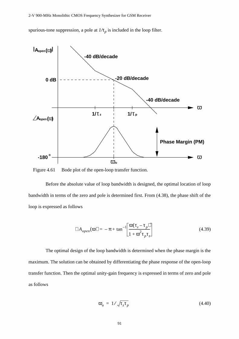
2-V 900-MHz Monolithic CMOS Frequency Synthesizer for GSM Receiver
91
spurious-tone suppression, a pole at1/τp is included in the loop filter.
Before the absolute value of loop bandwidth is designed, the optimal location of loop
bandwidth in terms of the zero and pole is determined first. From (4.38), the phase shift of the
loop is expressed as follows
(4.39)
The optimal design of the loop bandwidth is determined when the phase margin is the
maximum. The solution can be obtained by differentiating the phase response of the open-loop
transfer function. Then the optimal unity-gain frequency is expressed in terms of zero and pole
as follows
(4.40)
Aopen (ω)
Aopen (ω)| |
1/τp1/τz
uω-180
o
ω
ω
-40 dB/decade
-40 dB/decade
-20 dB/decade
Phase Margin (PM)
0 dB
Figure 4.61 Bode plot of the open-loop transfer function.
Aopen ω( )∠ π–ω τz τp–( )
1 ω2τpτz+--------------------------1–tan+=
ωu 1 τzτp⁄=
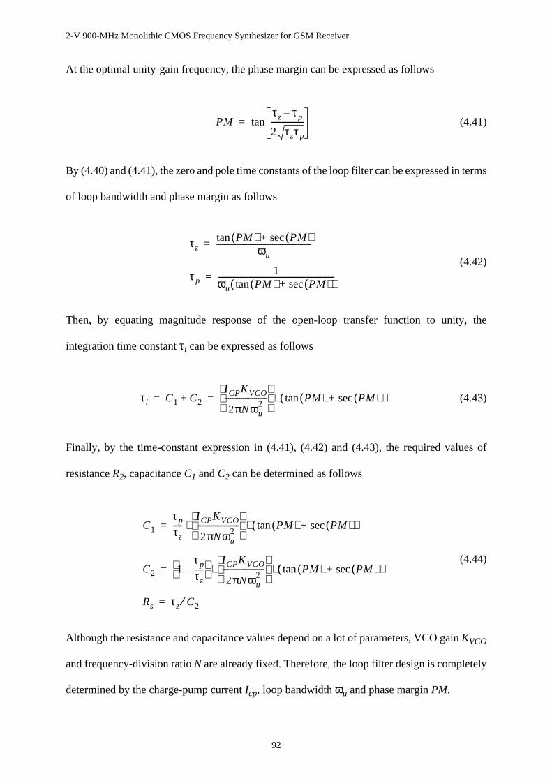
2-V 900-MHz Monolithic CMOS Frequency Synthesizer for GSM Receiver
92
At the optimal unity-gain frequency, the phase margin can be expressed as follows
(4.41)
By (4.40) and (4.41), the zero and pole time constants of the loop filter can be expressed in terms
of loop bandwidth and phase margin as follows
(4.42)
Then, by equating magnitude response of the open-loop transfer function to unity, the
integration time constantτi can be expressed as follows
(4.43)
Finally, by the time-constant expression in (4.41), (4.42) and (4.43), the required values of
resistanceR2, capacitanceC1 andC2 can be determined as follows
(4.44)
Although the resistance and capacitance values depend on a lot of parameters, VCO gainKVCO
and frequency-division ratioN are already fixed. Therefore, the loop filter design is completely
determined by the charge-pump currentIcp, loop bandwidthωu and phase marginPM.
PMτz τp–
2 τzτp
-----------------tan=
τzPM( ) PM( )sec+tan
ωu---------------------------------------------------=
τp1
ωu PM( ) PM( )sec+tan( )---------------------------------------------------------------=
τi C1 C2+I CPKVCO
2πNωu2
-----------------------
PM( ) PM( )sec+tan( )⋅= =
C1
τp
τz-----
I CPKVCO
2πNωu2
-----------------------
PM( ) PM( )sec+tan( )⋅ ⋅=
C2 1τp
τz-----–
I CPKVCO
2πNωu2
-----------------------
PM( ) PM( )sec+tan( )⋅ ⋅=
Rs τz C2⁄=

2-V 900-MHz Monolithic CMOS Frequency Synthesizer for GSM Receiver
93
4.9.7 Charge-Pump and Loop-Filter Design Optimization
After the detailed discussion of spurious tones, phase noise and loop stability of the
PLLs, this section discusses the design optimization of both the low-frequency and high
frequency loop.
4.9.7.1 Design Consideration
As stated in Section 4.9.1, the design requirement is to meet the phase-noise (< -121
dBc/Hz@600kHz) and spurious-tone specification (< -88 dBc) with minimum chip area.
From (4.43), it is found that the total capacitance is proportional to the charge-pump
currentIcp and phase marginPM, but inversely proportional to square of loop bandwidthωu.
Therefore, the optimal design requires small charge-pump current, small phase margin, and
large loop bandwidth.
Although small charge-pump current is desired, the current should be large enough to
be measurable by ammeter. On the other hand, the phase margin is typically limited between
45° and 60° to maintain loop stability against any process variation. As spurious tones cannot
be completely eliminated by only optimizing the charge-pump design, the maximum loop
bandwidth is limited by the spurious-tone performance.
4.9.7.2 High-Frequency Loop Design
From Figure 4.62, the VCO gain of the LC oscillator VCO2 varies from 75 to 275
MHz/V. However, such VCO gain variation only degrades the phase margin by less than 5° as
shown in Figure 4.62. Instead, it modifies the loop bandwidth between 15 and 40 kHz which is
still large enough for the GSM switching-time specification. Therefore, the phase margin of the
high-frequency loop is designed to be 45°.
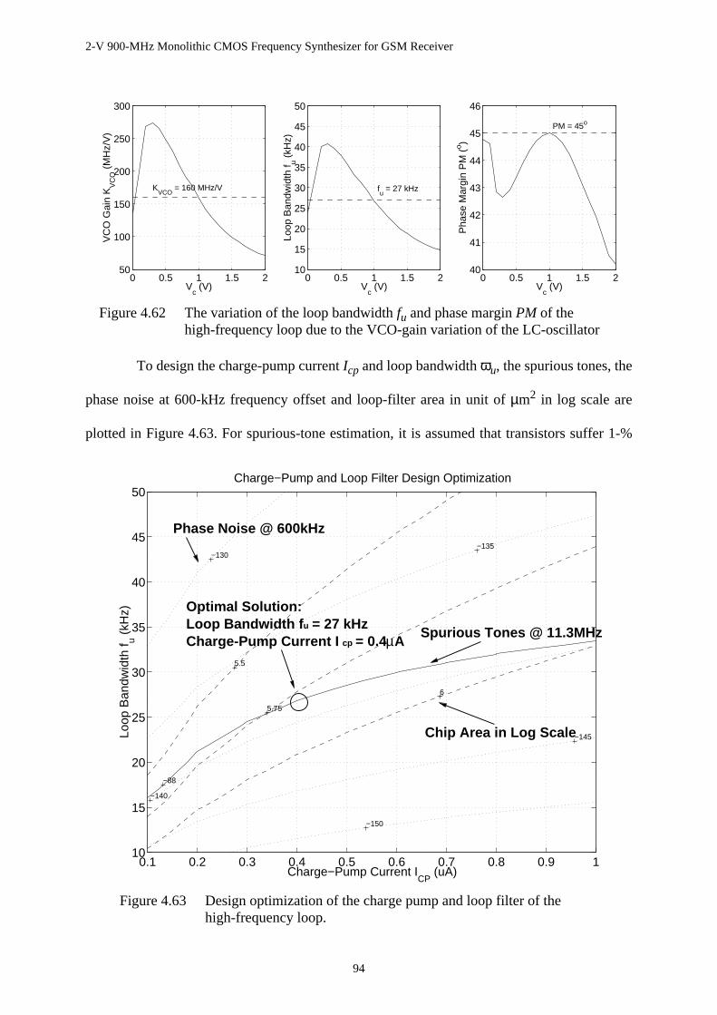
2-V 900-MHz Monolithic CMOS Frequency Synthesizer for GSM Receiver
94
To design the charge-pump currentIcp and loop bandwidthωu, the spurious tones, the
phase noise at 600-kHz frequency offset and loop-filter area in unit ofµm2 in log scale are
plotted in Figure 4.63. For spurious-tone estimation, it is assumed that transistors suffer 1-%
0 0.5 1 1.5 250
100
150
200
250
300
KVCO
= 160 MHz/V
Vc (V)
VC
O G
ain
KV
CO
(M
Hz/
V)
0 0.5 1 1.5 210
15
20
25
30
35
40
45
50
fu = 27 kHz
Vc (V)
Loop
Ban
dwid
th f u (
kHz)
0 0.5 1 1.5 240
41
42
43
44
45
46
PM = 45o
Vc (V)
Pha
se M
argi
n P
M (
o )
Figure 4.62 The variation of the loop bandwidthfu and phase marginPM of thehigh-frequency loop due to the VCO-gain variation of the LC-oscillator
0.1 0.2 0.3 0.4 0.5 0.6 0.7 0.8 0.9 110
15
20
25
30
35
40
45
50
−150
−145
−140
−135−130
−88
5.5
5.75
6
Charge−Pump Current ICP
(uA)
Loop
Ban
dwid
th f u (
kHz)
Charge−Pump and Loop Filter Design Optimization
u = 27 kHzCharge-Pump Current I cp = 0.4µA
Optimal Solution:Loop Bandwidth f
Phase Noise @ 600kHz
Spurious Tones @ 11.3MHz
Chip Area in Log Scale
Figure 4.63 Design optimization of the charge pump and loop filter of thehigh-frequency loop.
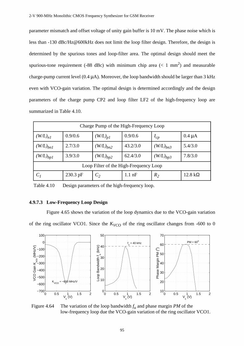
2-V 900-MHz Monolithic CMOS Frequency Synthesizer for GSM Receiver
95
parameter mismatch and offset voltage of unity gain buffer is 10 mV. The phase noise which is
less than -130 dBc/Hz@600kHz does not limit the loop filter design. Therefore, the design is
determined by the spurious tones and loop-filter area. The optimal design should meet the
spurious-tone requirement (-88 dBc) with minimum chip area (< 1 mm2) and measurable
charge-pump current level (0.4µA). Moreover, the loop bandwidth should be larger than 3 kHz
even with VCO-gain variation. The optimal design is determined accordingly and the design
parameters of the charge pump CP2 and loop filter LF2 of the high-frequency loop are
summarized in Table 4.10.
4.9.7.3 Low-Frequency Loop Design
Figure 4.65 shows the variation of the loop dynamics due to the VCO-gain variation
of the ring oscillator VCO1. Since theKVCO of the ring oscillator changes from -600 to 0
Charge Pump of the High-Frequency Loop
(W/L)n1 0.9/0.6 (W/L)p1 0.9/0.6 Icp 0.4µA
(W/L)bn1 2.7/3.0 (W/L)bn2 43.2/3.0 (W/L)bn3 5.4/3.0
(W/L)bp1 3.9/3.0 (W/L)bp2 62.4/3.0 (W/L)bp3 7.8/3.0
Loop Filter of the High-Frequency Loop
C1 230.3 pF C2 1.1 nF R2 12.8 kΩ
Table 4.10 Design parameters of the high-frequency loop.
0 0.5 1 1.5 2−700
−600
−500
−400
−300
−200
−100
0
100
KVCO
= −600 MHz/V
Vc (V)
VC
O G
ain
Kvc
o (M
Hz/
V)
0 0.5 1 1.5 20
10
20
30
40
50
fu = 40 kHz
Vc (V)
Loop
Ban
dwid
th f u (
kHz)
0 0.5 1 1.5 210
20
30
40
50
60
70
PM = 60o
Vc (V)
Pha
se M
argi
n P
M (
o )
Figure 4.64 The variation of the loop bandwidthfu and phase marginPM of thelow-frequency loop due the VCO-gain variation of the ring oscillator VCO1.
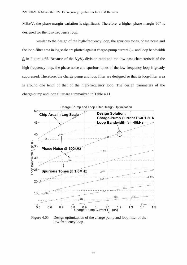
2-V 900-MHz Monolithic CMOS Frequency Synthesizer for GSM Receiver
96
MHz/V, the phase-margin variation is significant. Therefore, a higher phase margin 60° is
designed for the low-frequency loop.
Similar to the design of the high-frequency loop, the spurious tones, phase noise and
the loop-filter area in log scale are plotted against charge-pump currentICP and loop bandwidth
fu in Figure 4.65. Because of theN3/N2 division ratio and the low-pass characteristic of the
high-frequency loop, the phase noise and spurious tones of the low-frequency loop is greatly
suppressed. Therefore, the charge pump and loop filter are designed so that its loop-filter area
is around one tenth of that of the high-frequency loop. The design parameters of the
charge-pump and loop filter are summarized in Table 4.11.
0.5 0.6 0.7 0.8 0.9 1 1.1 1.2 1.3 1.4 1.510
15
20
25
30
35
40
45
50
−115
−110
−105
−100
−95
−185
−180
−175
−170
−165
160
4.5
4.75
55.25
5.5
5.75
6
Charge−Pump Current ICP
(uA)
Loop
Ban
dwid
th f u (
kHz)
Charge−Pump and Loop Filter Design Optimization
CP= 1.2uALoop Bandwidth f u = 40kHz
Design Solution:Charge-Pump Current I
Chip Area in Log Scale
Phase Noise @ 600kHz
Spurious Tones @ 1.6MHz
Figure 4.65 Design optimization of the charge pump and loop filter of thelow-frequency loop.

2-V 900-MHz Monolithic CMOS Frequency Synthesizer for GSM Receiver
97
4.9.8 Performance Summary of the Dual-Loop Frequency Synthesizer
With the phase-noise estimation of all the building blocks, the phase noise of the whole
dual-loop frequency synthesizer is plotted against offset frequency in Figure 4.66. It is found
that the close-in phase noise is dominated by transistorsMbn1a andMbp1a of the charge pump
Charge Pump of the Low-Frequency Loop
(W/L)n1 0.9/0.6 (W/L)p1 0.9/0.6 Icp 1.2µA
(W/L)bn1 7.5/3.0 (W/L)bn2 120/3.0 (W/L)bn3 15/3.0
(W/L)bp1 11.4/3.0 (W/L)bp2 182.4/3.0 (W/L)bp3 22.8/3.0
Loop Filter of the Low-Frequency Loop
C1 8.7 pF C2 113.1 pF R2 131.3 kΩ
Table 4.11 Design parameters of the charge pump and loop filter of the low-frequency loop.
102
103
104
105
106
−140
−130
−120
−110
−100
−90
−80
−70
Offset Frequency foff
(Hz)
Pha
se N
oise
(dB
c/H
z)
Phase Noise of the Dual−Loop Frequency Synthesizer
VCO1
VCO2
CP2 & LF2Total
CP1 & LF1
Figure 4.66 Phase noise of the whole dual-loop frequency synthesizer.

2-V 900-MHz Monolithic CMOS Frequency Synthesizer for GSM Receiver
98
CP1 while the high-offset phase noise is dominated by VCO2. The total phase noise of the
synthesizer is -123.8 dBc/Hz @ 600kHz.
After the discussion of design issues of all the building blocks, the performance such
as, phase noise, chip area and power consumption, are summarized in Table 4.12. The total
power consumption is 31.8 mW and the chip area is less than 2× 2 cm2.
Building Blocks Implementation Specification Performance
VCO1 Ring Oscillator -103 dBc/Hz @600kHz
Phase Noise = -112 dBc/HzPower = 10.2 mW
VCO2 LC Oscillator -121 dBc/Hz @600kHz
Phase Noise = -124 dBc/HzPower = 13.8 mW
Divider N1True-Single-Phase-Clock(TSPC) Logic
N1 = 226 ~ 349 Power = 2.2 mW
Divider N2 N2 = 32 Power = 0.6 mW
Divider N3 N3 = 4 Power = 5 mW
CP1 & LF1 Linear Capacitor& Silicide-BlockedPolysilicon
Area < 1 mm2 Area = 0.06 mm2
CP2 & LF2 Area < 1 mm2 Area = 0.6 mm2
Synthesizer Phase Noise< -121 dBc/Hz
Phase Noise= -123.8 dBc/Hz
Spurious Tones< -88 dBc
Spurious Tones= -88 dBc
Power< 50 mW
Power = 31.8 mW
Table 4.12 Performance summary of the dual-loop frequency synthesizer.
2-V 900-MHz Monolithic CMOS Frequency Synthesizer for GSM Receiver
99
Chapter 5
Layout
5.1 Introduction
In this chapter, the layout techniques which are critical for mixed-signal design are
discussed. Since noise coupling between digital parts and analog parts are critical factor which
limits the performance of the synthesizer, some special attentions are necessary to be made in
the layout process to minimize these effects.
5.2 Loop-Filter Capacitor Layout
The loop filter shown in Figure 4.53 consists of two capacitorsC1 & C2, and a resistor
R2. The capacitors are implemented by linear capacitors which provides a high
capacitance-to-area ratio. In order to maintain the capacitance ratio betweenC1 andC2 against
the process variation, two capacitors are inter-digitized and are arranged so that two capacitors
have similar centroid as shown in Figure 5.1.
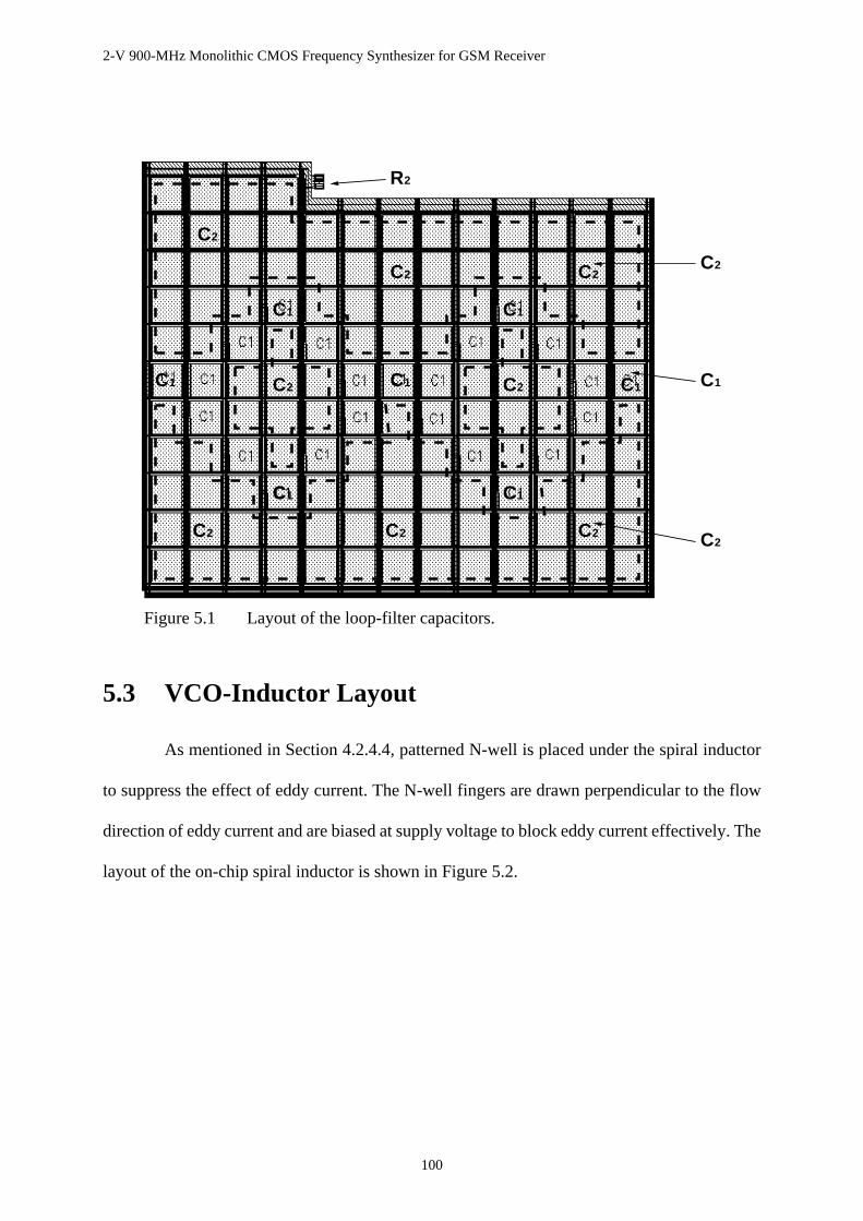
2-V 900-MHz Monolithic CMOS Frequency Synthesizer for GSM Receiver
100
5.3 VCO-Inductor Layout
As mentioned in Section 4.2.4.4, patterned N-well is placed under the spiral inductor
to suppress the effect of eddy current. The N-well fingers are drawn perpendicular to the flow
direction of eddy current and are biased at supply voltage to block eddy current effectively. The
layout of the on-chip spiral inductor is shown in Figure 5.2.
2
R2
C1 C2
C
C
C
1
C2
C2
C2
C
2
C1C
1
C1
C1
C2
C1
C2
C1
C2
2
Figure 5.1 Layout of the loop-filter capacitors.

2-V 900-MHz Monolithic CMOS Frequency Synthesizer for GSM Receiver
101
5.4 Supply-Line and Pad Layout
As the dual-loop frequency synthesizer consists of both the analog components and
digital components, care must be taken to eliminate the noise coupling between two portions.
To minimize the noise interaction of analog and digital power supplies, a decoupling filter is
placed in between. As shown in Figure 5.3, the bonding wires and the by-pass capacitors act as
the decoupling filter between the analog and digital portions [26].
Metal 2
Metal 3
Patterned N-Well Fingers
Figure 5.2 Layout of the VCO on-chip spiral inductor.
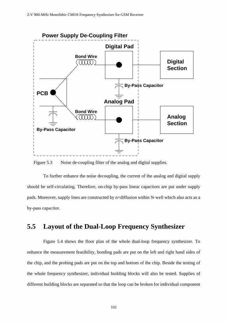
2-V 900-MHz Monolithic CMOS Frequency Synthesizer for GSM Receiver
102
To further enhance the noise decoupling, the current of the analog and digital supply
should be self-circulating. Therefore, on-chip by-pass linear capacitors are put under supply
pads. Moreover, supply lines are constructed by n+diffusion within N-well which also acts as a
by-pass capacitor.
5.5 Layout of the Dual-Loop Frequency Synthesizer
Figure 5.4 shows the floor plan of the whole dual-loop frequency synthesizer. To
enhance the measurement feasibility, bonding pads are put on the left and right hand sides of
the chip, and the probing pads are put on the top and bottom of the chip. Beside the testing of
the whole frequency synthesizer, individual building blocks will also be tested. Supplies of
different building blocks are separated so that the loop can be broken for individual component
AnalogSection
DigitalSection
Power Supply De-Coupling Filter
Digital Pad
Analog Pad
PCB
Bond Wire
Bond Wire
By-Pass Capacitor
By-Pass Capacitor
By-Pass Capacitor
Figure 5.3 Noise de-coupling filter of the analog and digital supplies.
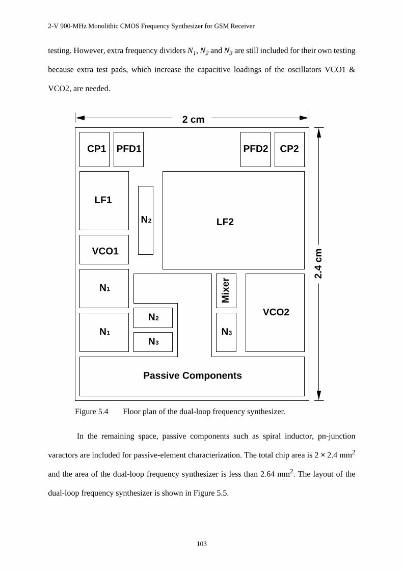
2-V 900-MHz Monolithic CMOS Frequency Synthesizer for GSM Receiver
103
testing. However, extra frequency dividersN1, N2 andN3 are still included for their own testing
because extra test pads, which increase the capacitive loadings of the oscillators VCO1 &
VCO2, are needed.
In the remaining space, passive components such as spiral inductor, pn-junction
varactors are included for passive-element characterization. The total chip area is 2× 2.4 mm2
and the area of the dual-loop frequency synthesizer is less than 2.64 mm2. The layout of the
dual-loop frequency synthesizer is shown in Figure 5.5.
N2
N2
N1
N1
N3
N3
LF2
VCO2
CP2PFD2PFD1CP1
LF1
VCO1
Mix
er
Passive Components
2 cm
2.4
cm
Figure 5.4 Floor plan of the dual-loop frequency synthesizer.
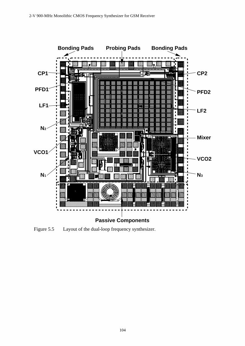
2-V 900-MHz Monolithic CMOS Frequency Synthesizer for GSM Receiver
104
3N1
N2
N
CP2
LF2
VCO2
Mixer
PFD2
CP1
PFD1
LF1
Bonding PadsBonding Pads Probing Pads
Passive Components
VCO1
Figure 5.5 Layout of the dual-loop frequency synthesizer.
2-V 900-MHz Monolithic CMOS Frequency Synthesizer for GSM Receiver
105
Chapter 6
Measurement
6.1 Introduction
The dual-loop frequency synthesizer is fabricated by the HP 0.5-µm
single-poly-triple-metal N-well CMOS technology. From the parametric test results provided
by HP, it is found that the device characteristics are closely matched with the simulation
parameters used in the design stage. Before the measurement of the whole synthesizer,
individual building blocks are measured and discussed.
6.2 LC Oscillator VCO2
6.2.1 Spiral Inductor & PN-Junction Varactor
The LC oscillator VCO2 consists of the LC tank and the negative transconductor. As
both the center frequency and phase noise are mainly determined by the quality factor of the LC
tank, the accuracy of the inductor and varactor are very important. The passive-component
measurement also verifies the accuracy of inductor and varactor modelling.
6.2.1.1 Test Setup
The setup shown in Figure 6.1 is adopted to characterize the passive components. The
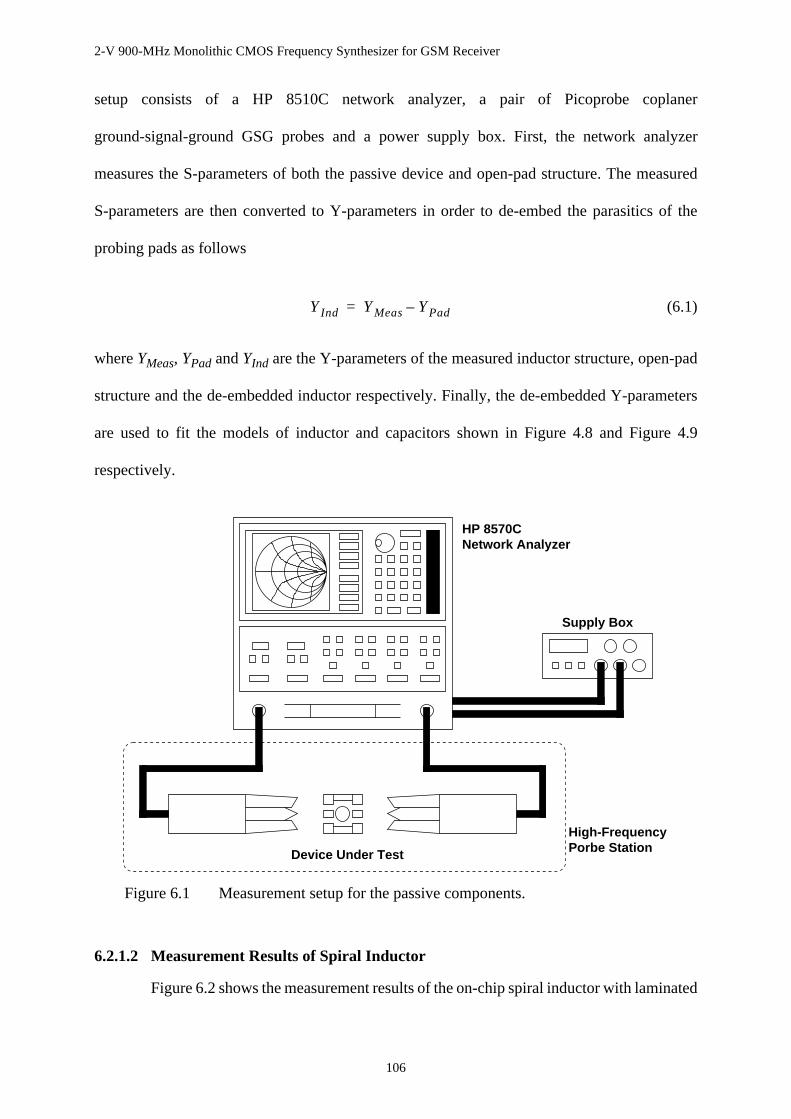
2-V 900-MHz Monolithic CMOS Frequency Synthesizer for GSM Receiver
106
setup consists of a HP 8510C network analyzer, a pair of Picoprobe coplaner
ground-signal-ground GSG probes and a power supply box. First, the network analyzer
measures the S-parameters of both the passive device and open-pad structure. The measured
S-parameters are then converted to Y-parameters in order to de-embed the parasitics of the
probing pads as follows
(6.1)
whereYMeas, YPad andYInd are the Y-parameters of the measured inductor structure, open-pad
structure and the de-embedded inductor respectively. Finally, the de-embedded Y-parameters
are used to fit the models of inductor and capacitors shown in Figure 4.8 and Figure 4.9
respectively.
6.2.1.2 Measurement Results of Spiral Inductor
Figure 6.2 shows the measurement results of the on-chip spiral inductor with laminated
YInd YMeas YPad–=
High-FrequencyPorbe Station
Supply Box
Device Under Test
HP 8570CNetwork Analyzer
Figure 6.1 Measurement setup for the passive components.
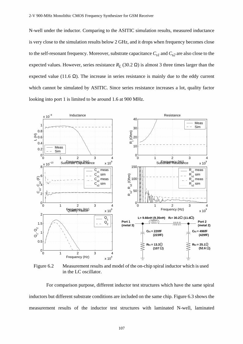
2-V 900-MHz Monolithic CMOS Frequency Synthesizer for GSM Receiver
107
N-well under the inductor. Comparing to the ASITIC simulation results, measured inductance
is very close to the simulation results below 2 GHz, and it drops when frequency becomes close
to the self-resonant frequency. Moreover, substrate capacitanceCs1 andCs2 are also close to the
expected values. However, series resistanceRL (30.2Ω) is almost 3 three times larger than the
expected value (11.6Ω). The increase in series resistance is mainly due to the eddy current
which cannot be simulated by ASITIC. Since series resistance increases a lot, quality factor
looking into port 1 is limited to be around 1.6 at 900 MHz.
For comparison purpose, different inductor test structures which have the same spiral
inductors but different substrate conditions are included on the same chip. Figure 6.3 shows the
measurement results of the inductor test structures with laminated N-well, laminated
0 1 2 3 4
x 109
0
0.2
0.4
0.6
0.8
1
x 10−8
Frequency (Hz)
L (H
)
Inductance
MeasSim
0 1 2 3 4
x 109
0
10
20
30
40
Frequency (Hz)
Rl (
Ohm
)
Resistance
MeasSim
0 1 2 3 4
x 109
0
2
4
6
8x 10
−13
Frequency (Hz)
Cs1
, Cs2
(F
)
Substrate Capacitance
Cs1
measC
s1 sim
Cs2
measC
s2 sim
0 1 2 3 4
x 109
0
50
100
150
Frequency (Hz)
Rs1
, Rs2
(O
hm)
Substrate Resistance
Rs1
measR
s1 sim
Rs2
measR
s2 sim
0 1 2 3 4
x 109
0
0.5
1
1.5
2
Frequency (Hz)
Q1, Q
2
Quality Factor
Q1
Q2
= 220fF(223fF)
CS1 = 496fF(429fF)
CS2
(107 Ω)= 13.3ΩRS1
(52.6 Ω)= 25.1ΩRS2
RL (11.6Ω)= 30.2ΩL= 9.66nH (9.35nH)Port 1(metal 3)
Port 2(metal 2)
Figure 6.2 Measurement results and model of the on-chip spiral inductor which is usedin the LC oscillator.

2-V 900-MHz Monolithic CMOS Frequency Synthesizer for GSM Receiver
108
polysilicon and only P-substrate under the inductors. Since only port 1 parameters are important
to the oscillator performance, port 2 parametersCS2, RS2 andQ2 are not shown for simplicity.
InductanceL of the three inductors are close to each other. As N-well fingers form junction
capacitance with P-substrate, the substrate capacitanceCS1 is reduced in the case with laminated
N-well. On the other hand, polysilicon fingers form additional capacitance, the substrate
capacitance is largest in this case. The series resistanceRL of the cases with laminated
polysilicon and only P-substrate are is only twice larger than that of the simulation results.
Comparing the series resistance between the structures with laminated polysilicon and with
only P-substrate, eddy current is induced only in substrate but not in polysilicon fingers. Since
the sheet resistance of polysilicon (2.2Ω/) is smaller than that of N-well (714Ω/), the
measurement results imply that the N-well fingers are not narrow enough such that eddy current
0 1 2 3 4
x 109
0
0.5
1
1.5
2x 10
−8
Frequency (Hz)
L (H
)
Inductance
N−wellPoly P−sub Sim
0 1 2 3 4
x 109
0
10
20
30
40
Frequency (Hz)
Rl (
Ohm
)
Resistance
N−wellPoly P−sub Sim
0 1 2 3 4
x 109
1
2
3
4
5x 10
−13
Frequency (Hz)
Cs1
(F
)
Port 1 Substrate Capacitance
N−wellPoly P−sub Sim
0 1 2 3 4
x 109
0
20
40
60
80
100
120
Frequency (Hz)
Rs1
(O
hm)
Port 1 Substrate Resistance
N−wellPoly P−sub Sim
0 1 2 3 4 5
x 109
0
0.5
1
1.5
2
2.5
Frequency (Hz)
Q1
Port 1 Quality Factor
N−wellPoly P−sub
Figure 6.3 Measurement results of the inductor test structures with laminated N-well,laminated polysilicon and only P-substrate under the inductors.
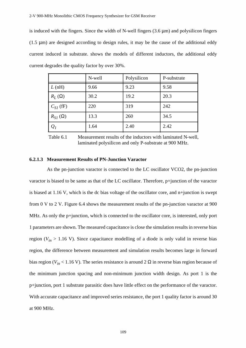
2-V 900-MHz Monolithic CMOS Frequency Synthesizer for GSM Receiver
109
is induced with the fingers. Since the width of N-well fingers (3.6µm) and polysilicon fingers
(1.5 µm) are designed according to design rules, it may be the cause of the additional eddy
current induced in substrate. shows the models of different inductors, the additional eddy
current degrades the quality factor by over 30%.
6.2.1.3 Measurement Results of PN-Junction Varactor
As the pn-junction varactor is connected to the LC oscillator VCO2, the pn-junction
varactor is biased to be same as that of the LC oscillator. Therefore, p+junction of the varactor
is biased at 1.16 V, which is the dc bias voltage of the oscillator core, and n+junction is swept
from 0 V to 2 V. Figure 6.4 shows the measurement results of the pn-junction varactor at 900
MHz. As only the p+junction, which is connected to the oscillator core, is interested, only port
1 parameters are shown. The measured capacitance is close the simulation results in reverse bias
region (Vin > 1.16 V). Since capacitance modelling of a diode is only valid in reverse bias
region, the difference between measurement and simulation results becomes large in forward
bias region (Vin < 1.16 V). The series resistance is around 2Ω in reverse bias region because of
the minimum junction spacing and non-minimum junction width design. As port 1 is the
p+junction, port 1 substrate parasitic does have little effect on the performance of the varactor.
With accurate capacitance and improved series resistance, the port 1 quality factor is around 30
at 900 MHz.
N-well Polysilicon P-substrate
L (nH) 9.66 9.23 9.58
RL (Ω) 30.2 19.2 20.3
CS1 (fF) 220 319 242
RS1 (Ω) 13.3 260 34.5
Q1 1.64 2.40 2.42
Table 6.1 Measurement results of the inductors with laminated N-well,laminated polysilicon and only P-substrate at 900 MHz.
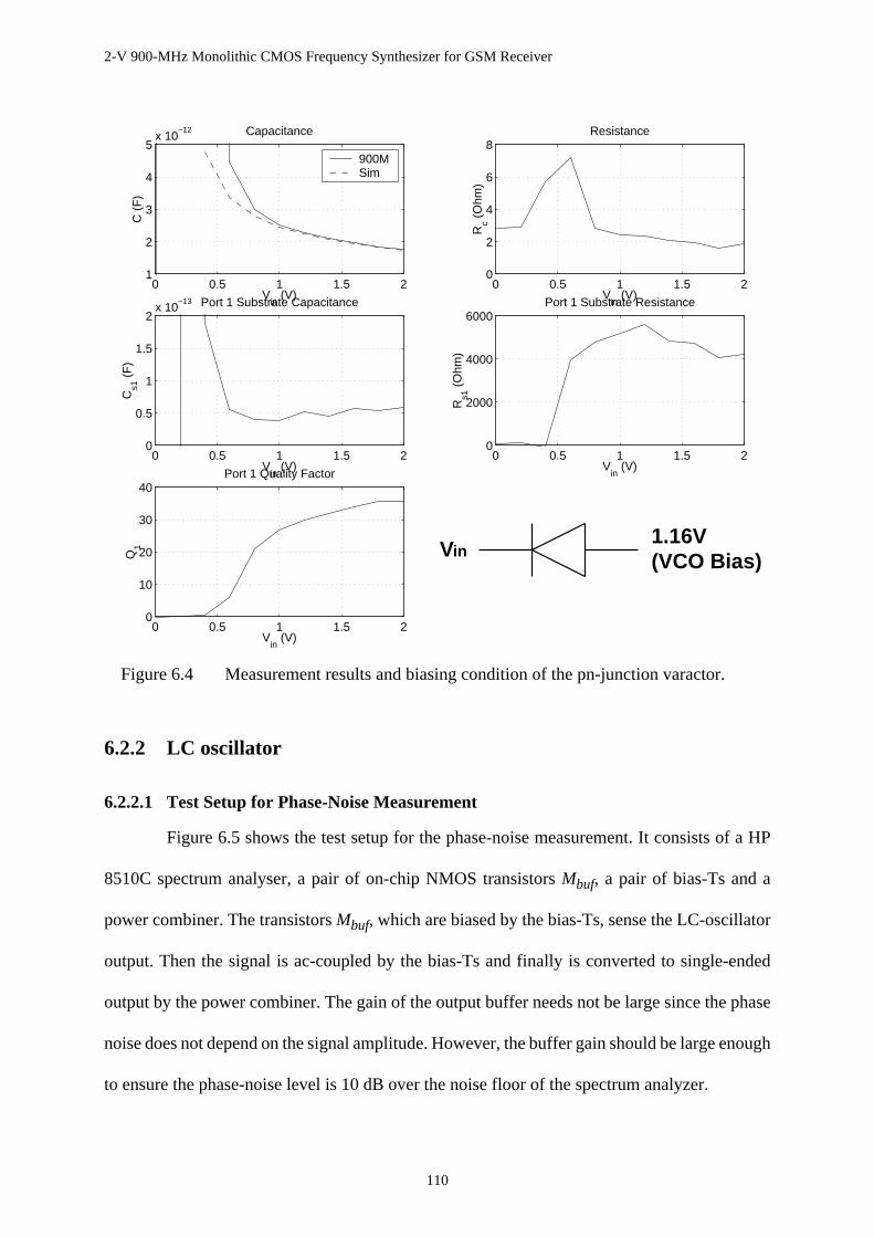
2-V 900-MHz Monolithic CMOS Frequency Synthesizer for GSM Receiver
110
6.2.2 LC oscillator
6.2.2.1 Test Setup for Phase-Noise Measurement
Figure 6.5 shows the test setup for the phase-noise measurement. It consists of a HP
8510C spectrum analyser, a pair of on-chip NMOS transistorsMbuf, a pair of bias-Ts and a
power combiner. The transistorsMbuf, which are biased by the bias-Ts, sense the LC-oscillator
output. Then the signal is ac-coupled by the bias-Ts and finally is converted to single-ended
output by the power combiner. The gain of the output buffer needs not be large since the phase
noise does not depend on the signal amplitude. However, the buffer gain should be large enough
to ensure the phase-noise level is 10 dB over the noise floor of the spectrum analyzer.
0 0.5 1 1.5 21
2
3
4
5x 10
−12
Vin
(V)
C (
F)
Capacitance
900MSim
0 0.5 1 1.5 20
2
4
6
8
Vin
(V)
Rc (
Ohm
)
Resistance
0 0.5 1 1.5 20
0.5
1
1.5
2x 10
−13
Vin
(V)
Cs1
(F
)
Port 1 Substrate Capacitance
0 0.5 1 1.5 20
2000
4000
6000
Vin
(V)R
s1 (
Ohm
)
Port 1 Substrate Resistance
0 0.5 1 1.5 20
10
20
30
40
Vin
(V)
Q1
Port 1 Quality Factor
Vin1.16V(VCO Bias)
Figure 6.4 Measurement results and biasing condition of the pn-junction varactor.
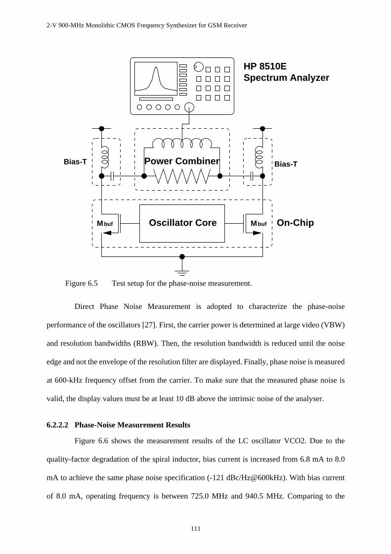
2-V 900-MHz Monolithic CMOS Frequency Synthesizer for GSM Receiver
111
Direct Phase Noise Measurement is adopted to characterize the phase-noise
performance of the oscillators [27]. First, the carrier power is determined at large video (VBW)
and resolution bandwidths (RBW). Then, the resolution bandwidth is reduced until the noise
edge and not the envelope of the resolution filter are displayed. Finally, phase noise is measured
at 600-kHz frequency offset from the carrier. To make sure that the measured phase noise is
valid, the display values must be at least 10 dB above the intrinsic noise of the analyser.
6.2.2.2 Phase-Noise Measurement Results
Figure 6.6 shows the measurement results of the LC oscillator VCO2. Due to the
quality-factor degradation of the spiral inductor, bias current is increased from 6.8 mA to 8.0
mA to achieve the same phase noise specification (-121 dBc/Hz@600kHz). With bias current
of 8.0 mA, operating frequency is between 725.0 MHz and 940.5 MHz. Comparing to the
Mbuf MbufOscillator Core
Bias-T Bias-TPower Combiner
On-Chip
HP 8510ESpectrum Analyzer
Figure 6.5 Test setup for the phase-noise measurement.
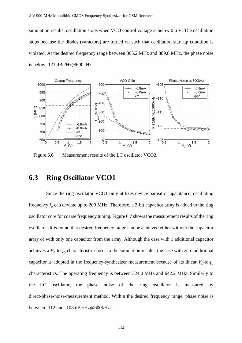
2-V 900-MHz Monolithic CMOS Frequency Synthesizer for GSM Receiver
112
simulation results, oscillation stops when VCO control voltage is below 0.6 V. The oscillation
stops because the diodes (varactors) are turned on such that oscillation start-up condition is
violated. At the desired frequency range between 865.2 MHz and 889.8 MHz, the phase noise
is below -121 dBc/Hz@600kHz.
6.3 Ring Oscillator VCO1
Since the ring oscillator VCO1 only utilizes device parasitic capacitance, oscillating
frequencyfo can deviate up to 200 MHz. Therefore, a 2-bit capacitor array is added to the ring
oscillator core for coarse frequency tuning. Figure 6.7 shows the measurement results of the ring
oscillator. It is found that desired frequency range can be achieved either without the capacitor
array or with only one capacitor from the array. Although the case with 1 additional capacitor
achieves aVc-to-fo characteristic closer to the simulation results, the case with zero additional
capacitor is adopted in the frequency-synthesizer measurement because of its linearVc-to-fo
characteristics. The operating frequency is between 324.0 MHz and 642.2 MHz. Similarly to
the LC oscillator, the phase noise of the ring oscillator is measured by
direct-phase-noise-measurement method. Within the desired frequency range, phase noise is
between -112 and -108 dBc/Hz@600kHz.
0 0.5 1 1.5 2650
700
750
800
850
900
950
1000
Vc (V)
f o (M
Hz)
Output Frequency
I=6.8mAI=8.0mASim Spec
0.5 1 1.5 20
100
200
300
400
500
600
Vc (V)
f vco (
MH
z/V
)
VCO Gain
I=6.8mAI=8.0mASim
0.5 1 1.5 2−125
−120
−115
−110
−105
Vc (V)
PN
(dB
c/H
z@60
0kH
z)
Phase Noise at 600kHz
I=6.8mAI=8.0mASpec
Figure 6.6 Measurement results of the LC oscillator VCO2.
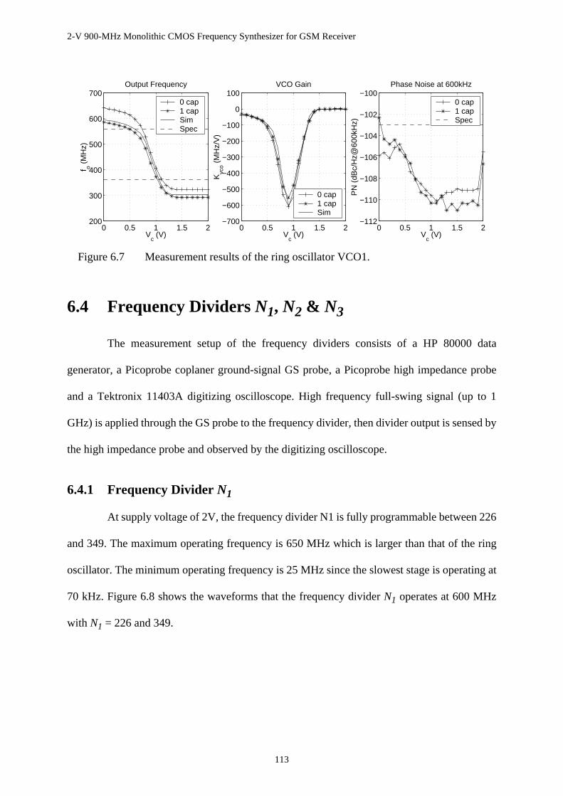
2-V 900-MHz Monolithic CMOS Frequency Synthesizer for GSM Receiver
113
6.4 Frequency DividersN1, N2 & N3
The measurement setup of the frequency dividers consists of a HP 80000 data
generator, a Picoprobe coplaner ground-signal GS probe, a Picoprobe high impedance probe
and a Tektronix 11403A digitizing oscilloscope. High frequency full-swing signal (up to 1
GHz) is applied through the GS probe to the frequency divider, then divider output is sensed by
the high impedance probe and observed by the digitizing oscilloscope.
6.4.1 Frequency DividerN1
At supply voltage of 2V, the frequency divider N1 is fully programmable between 226
and 349. The maximum operating frequency is 650 MHz which is larger than that of the ring
oscillator. The minimum operating frequency is 25 MHz since the slowest stage is operating at
70 kHz. Figure 6.8 shows the waveforms that the frequency dividerN1 operates at 600 MHz
with N1 = 226 and 349.
0 0.5 1 1.5 2200
300
400
500
600
700
Vc (V)
f o (M
Hz)
Output Frequency
0 cap1 capSim Spec
0 0.5 1 1.5 2−700
−600
−500
−400
−300
−200
−100
0
100
Vc (V)
Kvc
o (M
Hz/
V)
VCO Gain
0 cap1 capSim
0 0.5 1 1.5 2−112
−110
−108
−106
−104
−102
−100
Vc (V)
PN
(dB
c/H
z@60
0kH
z)
Phase Noise at 600kHz
0 cap1 capSpec
Figure 6.7 Measurement results of the ring oscillator VCO1.

2-V 900-MHz Monolithic CMOS Frequency Synthesizer for GSM Receiver
114
6.4.2 Frequency DividerN2
The frequency dividerN2 is tested in a similar way. At 2-V supply voltage, the
maximum operating frequency is 640 MHz which is larger than that of the ring oscillator VCO1.
The minimum operating frequency is less than 1 MHz. Figure 6.9 shows the waveforms of the
dividerN2 operating at 600 MHz.
Figure 6.8 Output waveforms of the programmable-frequency dividerN1 at 600 MHzwith (a)N1 = 226 and (b)N1 = 349.
(a) (b)

2-V 900-MHz Monolithic CMOS Frequency Synthesizer for GSM Receiver
115
6.4.3 Frequency DividerN3
Since frequency dividerN3 senses the sinusoidal output signal of the LC oscillator
VCO2, a HP E4422B signal generator and a bias-T are used to generate sinusoidal input signal
with dc bias. Under 2-V supply voltage, the operating frequency is larger than 1 GHz which is
larger than that of the LC oscillator. With input voltage of 0.5 V, input dc voltage can be
between 0.62 V and 1.32 V. With input dc bias of 1.1 V, which is the dc bias of the LC-oscillator
core, the minimum requirement input amplitude is 0.24 V. Figure 6.10 shows the waveforms of
the dividerN3 operating at 1 GHz.
Figure 6.9 Waveforms of the divide-by-32 frequency dividerN2 at 600 MHz.
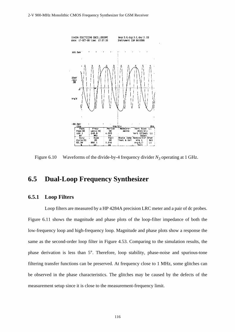
2-V 900-MHz Monolithic CMOS Frequency Synthesizer for GSM Receiver
116
6.5 Dual-Loop Frequency Synthesizer
6.5.1 Loop Filters
Loop filters are measured by a HP 4284A precision LRC meter and a pair of dc probes.
Figure 6.11 shows the magnitude and phase plots of the loop-filter impedance of both the
low-frequency loop and high-frequency loop. Magnitude and phase plots show a response the
same as the second-order loop filter in Figure 4.53. Comparing to the simulation results, the
phase derivation is less than 5°. Therefore, loop stability, phase-noise and spurious-tone
filtering transfer functions can be preserved. At frequency close to 1 MHz, some glitches can
be observed in the phase characteristics. The glitches may be caused by the defects of the
measurement setup since it is close to the measurement-frequency limit.
Figure 6.10 Waveforms of the divide-by-4 frequency dividerN3 operating at 1 GHz.
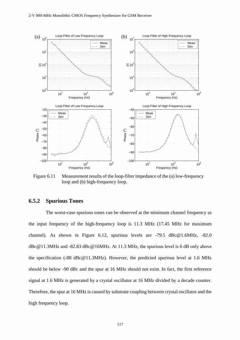
2-V 900-MHz Monolithic CMOS Frequency Synthesizer for GSM Receiver
117
6.5.2 Spurious Tones
The worst-case spurious tones can be observed at the minimum channel frequency as
the input frequency of the high-frequency loop is 11.3 MHz (17.45 MHz for maximum
channel). As shown in Figure 6.12, spurious levels are -79.5 [email protected], -82.0
[email protected] and -82.83 dBc@16MHz. At 11.3 MHz, the spurious level is 6 dB only above
the specification (-88 [email protected]). However, the predicted spurious level at 1.6 MHz
should be below -90 dBc and the spur at 16 MHz should not exist. In fact, the first reference
signal at 1.6 MHz is generated by a crystal oscillator at 16 MHz divided by a decade counter.
Therefore, the spur at 16 MHz is caused by substrate coupling between crystal oscillator and the
high frequency loop.
102
104
106
104
105
106
107
108
Frequency (Hz)
|z|
Loop Filter of Low Frequency Loop
MeasSim
102
104
106
103
104
105
106
107
Frequency (Hz)
|z|
Loop Filter of High Frequency Loop
MeasSim
102
104
106
−100
−90
−80
−70
−60
−50
−40
−30
−20
Frequency (Hz)
Pha
se (
o )
Loop Filter of Low Frequency Loop
MeasSim
102
104
106
−100
−90
−80
−70
−60
−50
−40
Frequency (Hz)
Pha
se (
o )
Loop Filter of High Frequency Loop
MeasSim
Figure 6.11 Measurement results of the loop-filter impedance of the (a) low-frequencyloop and (b) high-frequency loop.
(a) (b)

2-V 900-MHz Monolithic CMOS Frequency Synthesizer for GSM Receiver
118
Since there exists substrate coupling between the crystal oscillator and the
high-frequency loop, it is suspected that the large spurious level at 1.6 MHz is caused by
substrate coupling between the decade counter and the high-frequency loop. To verify the
assumption, the low-frequency loop is turned off and external input signal at 11.3 MHz is
applied to the high-frequency loop. Figure 6.13 shows that spurious level is -75.1
[email protected] and it implies the increase in spurious level at 1.6 MHz is due to the substrate
coupling.
@11.3 MHz-82.83 dBc@16 MHz
-79.5 [email protected] MHz -82.0 dBc
Figure 6.12 Measurement results of the spurious tones atfo = 865.2 MHz.
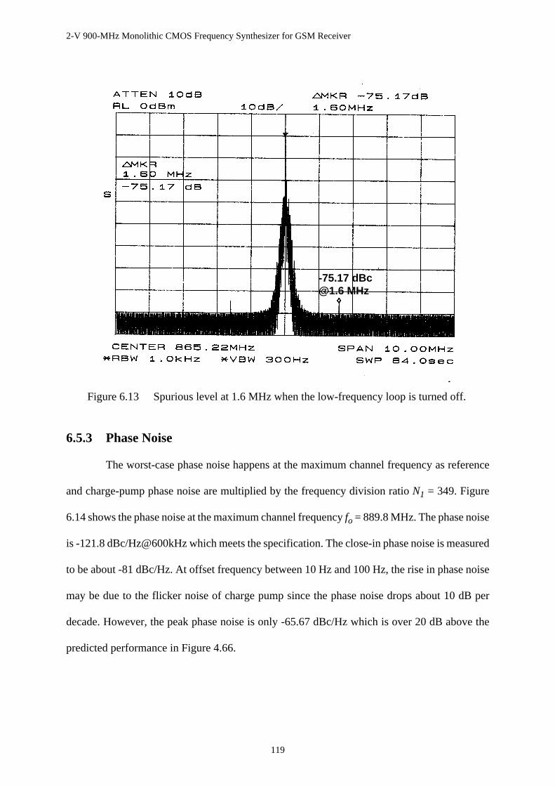
2-V 900-MHz Monolithic CMOS Frequency Synthesizer for GSM Receiver
119
6.5.3 Phase Noise
The worst-case phase noise happens at the maximum channel frequency as reference
and charge-pump phase noise are multiplied by the frequency division ratioN1 = 349. Figure
6.14 shows the phase noise at the maximum channel frequencyfo = 889.8 MHz. The phase noise
is -121.8 dBc/Hz@600kHz which meets the specification. The close-in phase noise is measured
to be about -81 dBc/Hz. At offset frequency between 10 Hz and 100 Hz, the rise in phase noise
may be due to the flicker noise of charge pump since the phase noise drops about 10 dB per
decade. However, the peak phase noise is only -65.67 dBc/Hz which is over 20 dB above the
predicted performance in Figure 4.66.
@1.6 MHz-75.17 dBc
Figure 6.13 Spurious level at 1.6 MHz when the low-frequency loop is turned off.

2-V 900-MHz Monolithic CMOS Frequency Synthesizer for GSM Receiver
120
6.5.4 Switching Time
6.5.4.1 Test Setup for Switching-Time Measurement
The test setup for switching time measurement is shown in Figure 6.15. It consists of
a SRS DS345 synthesized function generator, two Philips 74HC157D 4-bit multiplexers, two
dc probes and a HP 54520A general-purpose oscilloscope. The function generator applies clock
signal to the 4-bit multiplexers in order to program the frequency division ratioN1. When the
synthesizer switches between two channels at a very low frequency (e.g. 1 Hz), the switching
can be observed in the spectrum analyzer.
@15kHz
-121.8 dBc/Hz@600kHz
-65.67 dBc/Hz-62.8 dBc/Hz
-81.3 dBc/Hz
Figure 6.14 Measurement results of the phase noise atfo = 889.8 MHz.
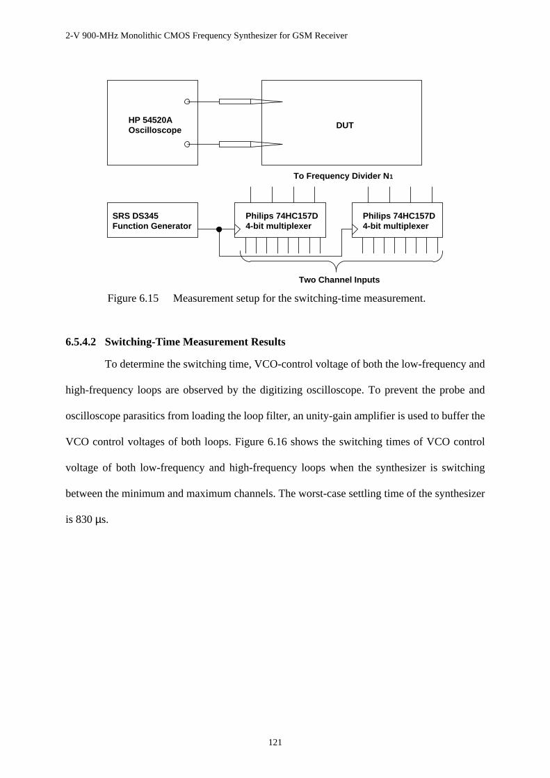
2-V 900-MHz Monolithic CMOS Frequency Synthesizer for GSM Receiver
121
6.5.4.2 Switching-Time Measurement Results
To determine the switching time, VCO-control voltage of both the low-frequency and
high-frequency loops are observed by the digitizing oscilloscope. To prevent the probe and
oscilloscope parasitics from loading the loop filter, an unity-gain amplifier is used to buffer the
VCO control voltages of both loops. Figure 6.16 shows the switching times of VCO control
voltage of both low-frequency and high-frequency loops when the synthesizer is switching
between the minimum and maximum channels. The worst-case settling time of the synthesizer
is 830µs.
Philips 74HC157D4-bit multiplexer
Philips 74HC157D4-bit multiplexer
To Frequency Divider N 1
SRS DS345Function Generator
HP 54520AOscilloscope
Two Channel Inputs
DUT
Figure 6.15 Measurement setup for the switching-time measurement.

2-V 900-MHz Monolithic CMOS Frequency Synthesizer for GSM Receiver
122
6.6 Performance Comparison
After the measurement of the whole dual-loop frequency synthesizer, Table 6.1
summaries the performance of different monolithic frequency synthesizer design published in
recent years for comparison purpose. For fair phase-noise comparison, all the phase-noise
performance is recalculated to an equivalent offset frequency of 600 kHz, assuming a
dependence of 20 dB per decade on offset frequency.
Design (1) is designed for the application of DCS 1800 which has similar specification
to GSM 900 except that the synthesizer operates at 1.8 GHz. By using fractional-N architecture,
input frequency can be designed at 26.6 MHz which is twice of the input frequency of the high
Figure 6.16 VCO control voltages of the low-frequency and high-frequency loopsswitching between the minimum and maximum channels.
0 0.5 1 1.5 2 2.5 3
x 10−3
0.9
1
1.1
1.2
1.3
1.4
Time (s)
Vc−
lfl (
V)
Settling of the Low−Frequency Loop
0 0.5 1 1.5 2 2.5 3
x 10−3
1.1
1.15
1.2
1.25
1.3
1.35
1.4
Time (s)
Vc−
hfl (
V)
Settling of the High−Frequency Loop
200 us200 us
560 us 830 us
2-V 900-MHz Monolithic CMOS Frequency Synthesizer for GSM Receiver
123
frequency loop. Therefore, loop bandwidth can be designed at 45 kHz to achieve a switching
time of 250µs. However, the loop filter is implemented by two layers of polysilicon, which the
unit capacitance is only 1.5 fF/µm2, the chip area is larger the dual-loop design. Moreover,
design (1) operates at 3-V supply, so its power consumption is around 33% larger than this
work.
Design (2) also adopts fractional-N design with input frequency of 9.6 MHz. This
design achieves the best spurious level below -110 dBc. However, the chip area is the biggest
one (5.5 mm2) although external loop filter is adopted. Moreover, the power consumption is
around 33% larger than this work since it operates at 2.7-V supply voltage.
Design (3) also adopts fractional-N architecture. Since this design only aims to achieve
600-kHz channel spacing, 61.6-MHz input reference is adopted and the loop bandwidth is
designed at 200 kHz which is 7 times larger than the dual-loop design. However, this design has
larger current consumption but its phase-noise performance is even worse than the dual-loop
design.
From the above comparison with the other existing monolithic frequency-synthesizer
solutions, it is found that the dual-loop frequency synthesizer satisfies the phase-noise
specification at 600-kHz frequency offset and switching-time specification for GSM 900.
Spurious level is limited to be -79.5 dBc because of substrate coupling of reference signal,
which also exists in design (1) and (3). Since the dual-loop design operates under 2-V supply,
its power consumption is at least 33% lower than the other designs. According to the design
optimization in Figure 4.63 and Figure 4.65, the loop-filter area of the low-frequency loop is
only one-tenth of that of the high-frequency loop. Therefore, the chip area of the dual-loop
design is just the average among the designs mentioned above with the help of linear capacitor,
where unit capacitance is 2.4 fF/µm2.
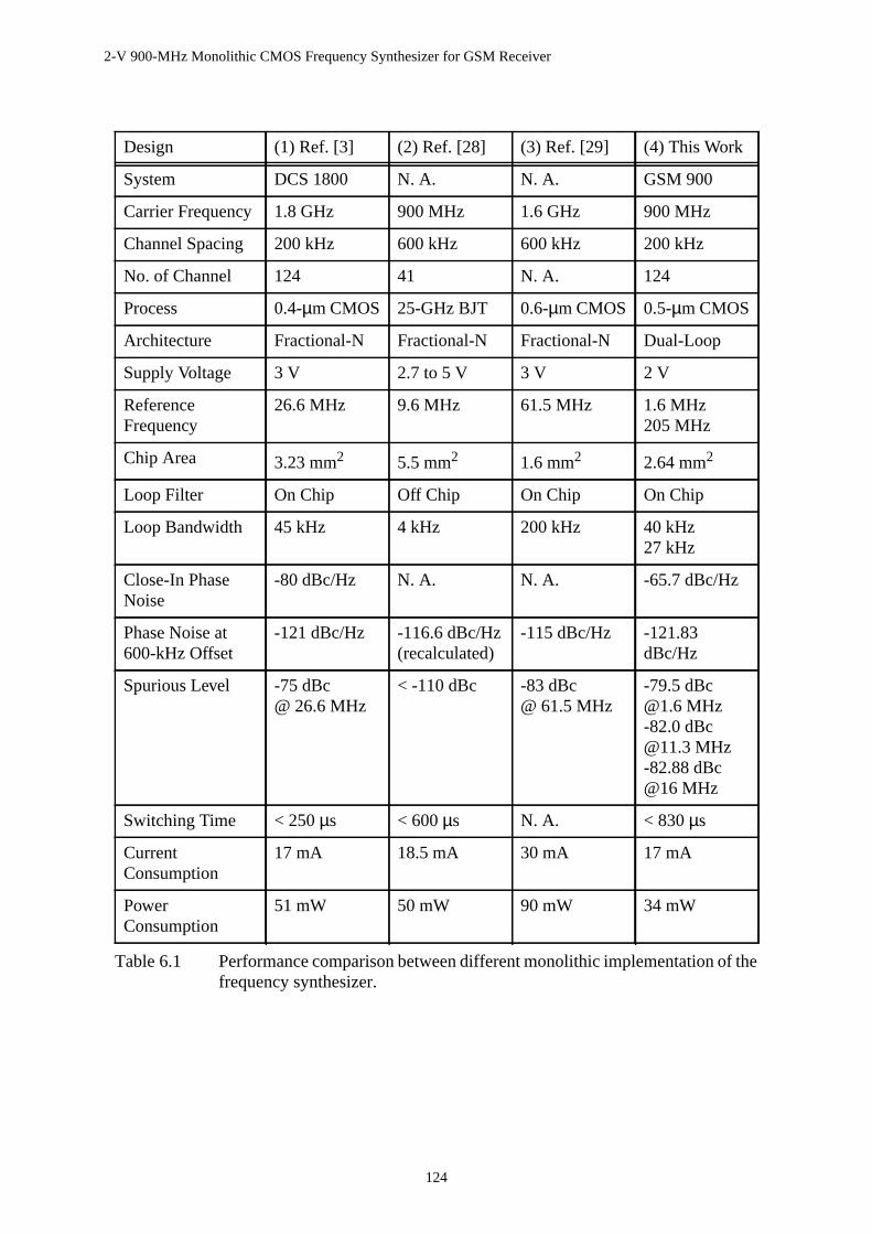
2-V 900-MHz Monolithic CMOS Frequency Synthesizer for GSM Receiver
124
Design (1) Ref. [3] (2) Ref. [28] (3) Ref. [29] (4) This Work
System DCS 1800 N. A. N. A. GSM 900
Carrier Frequency 1.8 GHz 900 MHz 1.6 GHz 900 MHz
Channel Spacing 200 kHz 600 kHz 600 kHz 200 kHz
No. of Channel 124 41 N. A. 124
Process 0.4-µm CMOS 25-GHz BJT 0.6-µm CMOS 0.5-µm CMOS
Architecture Fractional-N Fractional-N Fractional-N Dual-Loop
Supply Voltage 3 V 2.7 to 5 V 3 V 2 V
ReferenceFrequency
26.6 MHz 9.6 MHz 61.5 MHz 1.6 MHz205 MHz
Chip Area 3.23 mm2 5.5 mm2 1.6 mm2 2.64 mm2
Loop Filter On Chip Off Chip On Chip On Chip
Loop Bandwidth 45 kHz 4 kHz 200 kHz 40 kHz27 kHz
Close-In PhaseNoise
-80 dBc/Hz N. A. N. A. -65.7 dBc/Hz
Phase Noise at600-kHz Offset
-121 dBc/Hz -116.6 dBc/Hz(recalculated)
-115 dBc/Hz -121.83dBc/Hz
Spurious Level -75 dBc@ 26.6 MHz
< -110 dBc -83 dBc@ 61.5 MHz
-79.5 [email protected] MHz-82.0 [email protected] MHz-82.88 dBc@16 MHz
Switching Time < 250µs < 600µs N. A. < 830µs
CurrentConsumption
17 mA 18.5 mA 30 mA 17 mA
PowerConsumption
51 mW 50 mW 90 mW 34 mW
Table 6.1 Performance comparison between different monolithic implementation of thefrequency synthesizer.
2-V 900-MHz Monolithic CMOS Frequency Synthesizer for GSM Receiver
125
Chapter 7
Conclusion
This master thesis presents the design of a 2-V 900-MHz monolithic CMOS dual-loop
frequency synthesizer for GSM receivers with good phase-noise performance.
Designing fully integrated frequency synthesizers for system integration is always
desirable but most challenging. This first requirement is to achieve high frequency operation
with reasonable power consumption. However, the most critical challenges for the frequency
synthesizer are the phase-noise and spurious-tone performance. Finally, small chip area is
essential to monolithic system integration.
The dual-loop design consists of two reference signals and two phase-locked loops
(PLLs) in cascode configuration. Because of the dual-loop architecture, input frequencies of the
two PLLs are scaled from 200 kHz to 1.6 MHz and 11.3 MHz. Therefore, the loop bandwidths
of both PLLs can be increased, so that both switching time and chip area can be reduced.
Measurement of the on-chip spiral inductor shows the quality factor drops from 3 to
1.6. The quality-factor degradation is mainly due to additional eddy current induced in the
N-well fingers under the inductor, which is proven by the measurement results of the inductors
with laminated polysilicon and with only P-substrate.
Because of the quality-factor degradation of inductor, bias current of the LC oscillator
is increased from 6.8 mA to 8.0 mA in order to satisfy the phase-noise requirement. The
2-V 900-MHz Monolithic CMOS Frequency Synthesizer for GSM Receiver
126
phase-noise performance of the whole dual-loop frequency synthesizer is close to the estimation
except that the peak-close-in phase noise is 15 dB worse than the specification.
The spurious tones are -79.5 [email protected], -82.0 [email protected] and -82.88
dBc@16MHz, which are limited by substrate coupling. This assumption is verified by turning
off the low-frequency loop and spurious tones are still observed at with similar spurious level
at these frequencies.
Implemented in a 0.5-µm CMOS technology and at 2-V supply voltage, the dual-loop
frequency synthesizer has a low power consumption of 34 mW. At 900 MHz, the phase noise
of the dual-loop design is less than -121.83 dBc/Hz at 600-kHz frequency offset. The spurious
tones are -79.5 [email protected], -82.0 [email protected] and -82.88 dBc@16MHz. The worst-case
switching time is less than 830µs. The chip area is 2.64 mm2. However, the peak close-in phase
noise is -65.67 dBc/Hz at 15-kHz frequency offset which is 15 dB worse than the specification
of GSM 900.
2-V 900-MHz Monolithic CMOS Frequency Synthesizer for GSM Receiver
127
Bibliography
[1] Derek K. Shaeffer and Thomas H. Lee, “A 1.5-V, 1.5-GHz CMOS Low NoiseAmplifier,” IEEE Journal of Solid-State Circuits, vol. 32, no. 5, pp. 745-59, May 1997.
[2] Ricky K. C. Mak, Howard C. Luong, “A MOS Analog Mixer Using a Cross-CoupledPair With Source Followers,”Proceedings of the IEEE Asia Pacific Conference onCircuits and Systems 1996, pp. 117-20, 1996.
[3] J. Craninckx, M. Steyaert, “A Fully Integrated CMOS DSC-1800 FrequencySynthesizer,”IEEE Journal of Solid-State Circuits, vol. 33, no. 12, pp. 2054-65, Dec.1998.
[4] B. Razavi,RF Microelectronics, Prentice Hall, New Jersey, 1998.
[5] ETSI, “Digital cellular telecommunications system (Phase 2+); Radio transmissionand reception (GSM 5.05),”European Telecommunications Standards Institute,Copyright 1996.
[6] C. M. Hung, and Keneth K. O, “A 1.24-GHz Monolithic CMOS VCO with PhaseNoise of -137 dBc/Hz at a 3-MHz Offset,” IEEE Microwave and Guided Wave Letters,vol. 9, no. 3, March 1999.
[7] T. Aytur, J. Khony, “Advantages of Dual-Loop Frequency Synthesizers for GSMApplications,” Proceedings of the IEEE International Symposium of Circuits &System, 1997.
[8] N. M. Nguyen, R. G. Meyer, “Start-up and Frequency Stability in High-FrequencyOscillators,” IEEE Journal of Solid-State Circuits, vol. 27, no. 5, pp. 810-20, May1992.
[9] A. Hajimiri, T. H. Lee, “A General Theory of Phase Noise in Electrical Oscillators,”IEEE Journal of Solid-State Circuits, vol. 33, no. 2, pp. 179-94, Feb. 1998.
[10] J. R. Long, M. A. Copeland, “The Modelling, Characterization, and Design ofMonolithic Inductors for Silicon RF IC’s,”IEEE Journal of Solid-State Circuits, vol.32, no. 3, pp. 357-69, Mar 1997.
[11] J. Craninckx, M. Steyaert, “A 1.8-GHz Low-Phase-Noise CMOS VCO UsingOptimized Hollow Spiral Inductors,”IEEE Journal of Solid-State Circuits, vol. 32, no.5, pp. 736-44, May 1997.
2-V 900-MHz Monolithic CMOS Frequency Synthesizer for GSM Receiver
128
[12] R. B. Merrill, T. W. Lee, H. You, R. Rasmussen, L. A. Moberly, “Optimization of HighQ Integrated Inductors for Multi-Level Metal CMOS,”Proceedings of theInternational Electronic Device Meeting 1995, pp. 983-6, 1995.
[13] A. M. Niknejad, R. G. Meyer, “Analysis, Design, and Optimization of Spiral Inductorsand Transformers for Si RF IC’s,”IEEE Journal of Solid-State Circuits, vol. 33, no.10,Oct. 1998.
[14] CADENCE,Oscillator Noise Analysis in SpectreRF, application note to SpectreRF,1998.
[15] B. Chang, J. Park and W. Kim, “A 1.2-GHz CMOS Dual-Modulus Prescaler UsingNew Dynamic D-Type Flip-Flops”,IEEE Journal of Solid-State Circuits, vol. 31, no.5, pp. 749-52, May 1996.
[16] J. Yuan, and C. Svensson, “High-Speed CMOS Circuit Technique,”IEEE Journal ofSolid-State Circuits, vol. 24, no. 1, pp. 62-70, Feb. 1989.
[17] C. H. Park, B. Kim, “A Low-Noise, 900-MHz VCO in 0.6-µm CMOS,”IEEE Journalof Solid-State Circuits, vol. 34, pp. 586-91, May 1999.
[18] A. Hajimiri, S. Limotyrakis, T. H. Lee, “Phase Noise in Multi-Gigahertz CMOS RingOscillators,”Proceedings of the IEEE 1998 Custom Integrated Circuit Conference, pp.49-52, 1998.
[19] P. Larsson, “High-Speed Architecture for a Programmable Frequency Divider and aDual-Modulus Prescaler,”IEEE Journal of Solid-State Circuits, vol. 31, no. 5, May1996.
[20] J. R. Yuan, and C. Svensson, “Fast CMOS Non-binary Divider and Counter,”Electronics Letters, vol. 29, no. 13, 24th June 1993.
[21] J. R. Yuan, I. Karlsson, and C. Svensson, “A True Single-Phase-Clock DynamicCMOS Circuit Technique,”IEEE Journal of Solid-State Circuits, vol. 22, no. 5, Oct.1987.
[22] R. Ahola, J. Vikla, S. Lindfors, J. Routama, and K. Halonen, “A 2-GHz Phase-LockedLoop Frequency Synthesizer with On-Chip VCO,”Kluwer Academic Publishers.Analog Integrated Circuits and Signal Processing, vol. 18, no. 1, p. 43-54, Jan. 1999.
[23] W. H. Lee, J. D. Cho, and S. D. Lee, “A High Speed and Low Power Phase-FrequencyDetector and Charge-Pump,”
[24] Q. Huang, and R. Rogenmoser, “Speed Optimization of Edge-Triggered CMOSCircuits for Giga-Hertz Single-Phase Clocks,”IEEE Journal of Solid-State Circuits,vol. 31, no. 3, pp. 456-65, Mar. 1996.

2-V 900-MHz Monolithic CMOS Frequency Synthesizer for GSM Receiver
129
[25] I. A. Young, J. K. Greason, K. L. Wong, “PLL Clock Generator with 5 to 110 MHz ofLock Range for Microprocessors,”IEEE Journal of Solid-State Circuits, vol. 27, no.11, pp. 1599-607, Nov. 1992.
[26] M. Ismail, T. Fiez,Analog VLSI Signal and Information Processing, McGraw-Hill Inc.
[27] T. Friedrich, “Direct Phase Noise Measurements Using a Modern SpectrumAnalyzer”,Microwave Journal, vol. 35, pp. 94-104, Aug. 1992.
[28] A. Ali, J. L. Tham, “A 900-MHz Frequency Synthesizer with Integrated LCVoltage-Controlled Oscillator,”Proceedings of the IEEE International Solid-StateCircuits Conference 1996, pp. 390-1, 1996.
[29] J. F. Parker, and D. Ray, “A 1.6-GHz CMOS PLL with On-Chip Loop Filter,”IEEEJournal of Solid-State Circuits, vol. 33, no. 3, Mar. 1998.