Homemade Field Effect Transistor (FET) - SRJCsrjcstaff.santarosa.edu/~yataiiya/E45/PROJECTS/Homemade...
18
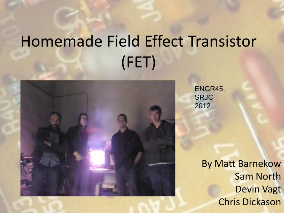
Homemade Field Effect Transistor (FET) By Matt Barnekow Sam North Devin Vagt Chris Dickason ENGR45, SRJC 2012
Transcript of Homemade Field Effect Transistor (FET) - SRJCsrjcstaff.santarosa.edu/~yataiiya/E45/PROJECTS/Homemade...
Homemade Field Effect Transistor (FET)
By Matt Barnekow Sam North Devin Vagt
Chris Dickason
ENGR45, SRJC 2012
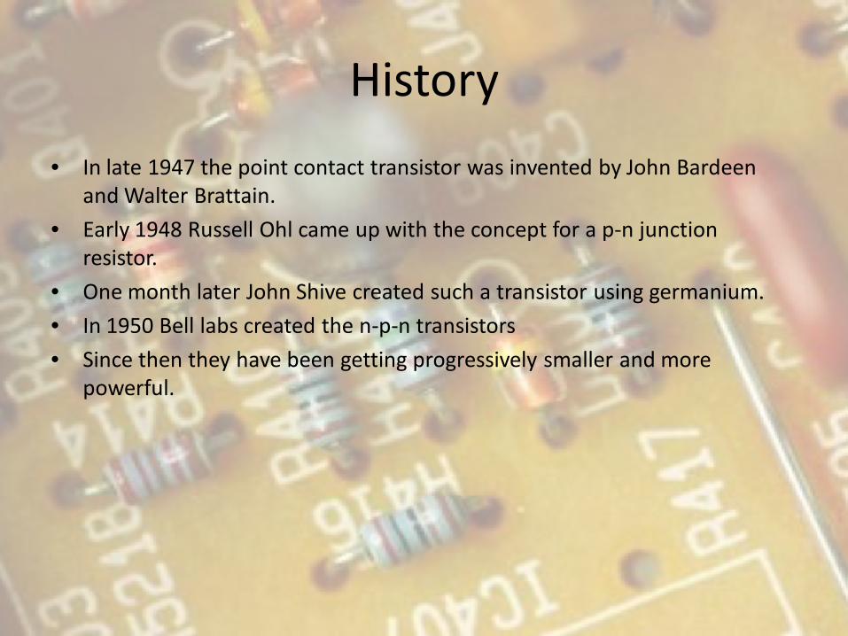
History
• In late 1947 the point contact transistor was invented by John Bardeen and Walter Brattain.
• Early 1948 Russell Ohl came up with the concept for a p-n junction resistor.
• One month later John Shive created such a transistor using germanium.
• In 1950 Bell labs created the n-p-n transistors
• Since then they have been getting progressively smaller and more powerful.

What is a Field Effect Transistor(FET)
• In a FET, the width of the conducting channel in a semiconductor and it’s current carrying capability is varied by the application of an electric field.
• Metal Oxide Semiconductor FET (MOSFET)
• Junction FET (JFET)
• Most commonly used is MOSFET which is manufactured as an enhancement or depletion type.
• Consists of a source, a gate and a drain.
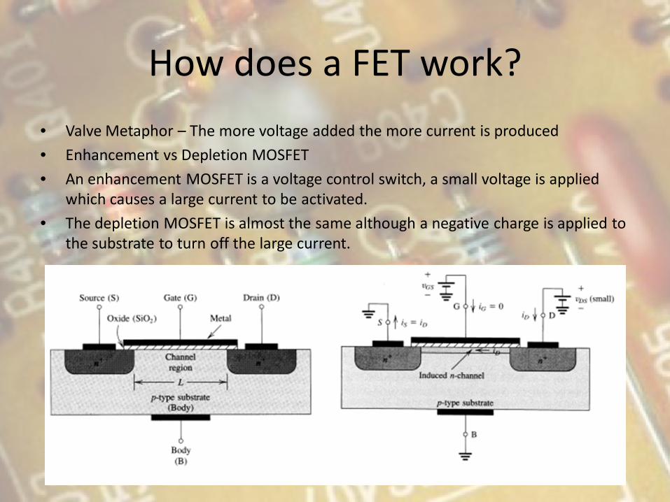
How does a FET work?
• Valve Metaphor – The more voltage added the more current is produced
• Enhancement vs Depletion MOSFET
• An enhancement MOSFET is a voltage control switch, a small voltage is applied which causes a large current to be activated.
• The depletion MOSFET is almost the same although a negative charge is applied to the substrate to turn off the large current.
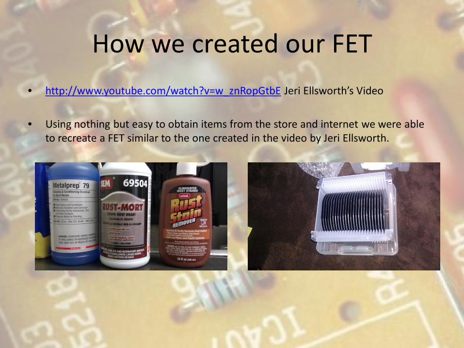
How we created our FET
• http://www.youtube.com/watch?v=w_znRopGtbE Jeri Ellsworth’s Video
• Using nothing but easy to obtain items from the store and internet we were able to recreate a FET similar to the one created in the video by Jeri Ellsworth.
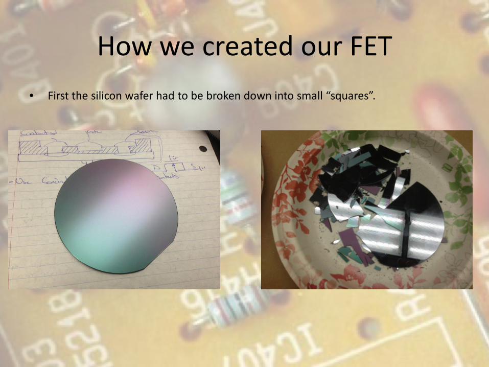
How we created our FET
• First the silicon wafer had to be broken down into small “squares”.
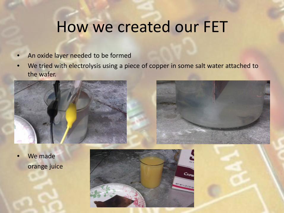
How we created our FET
• An oxide layer needed to be formed
• We tried with electrolysis using a piece of copper in some salt water attached to the wafer.
• We made
orange juice
How we created our FET
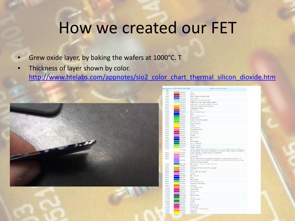
• Grew oxide layer, by baking the wafers at 1000°C. T
• Thickness of layer shown by color. http://www.htelabs.com/appnotes/sio2_color_chart_thermal_silicon_dioxide.htm
How we created our FET
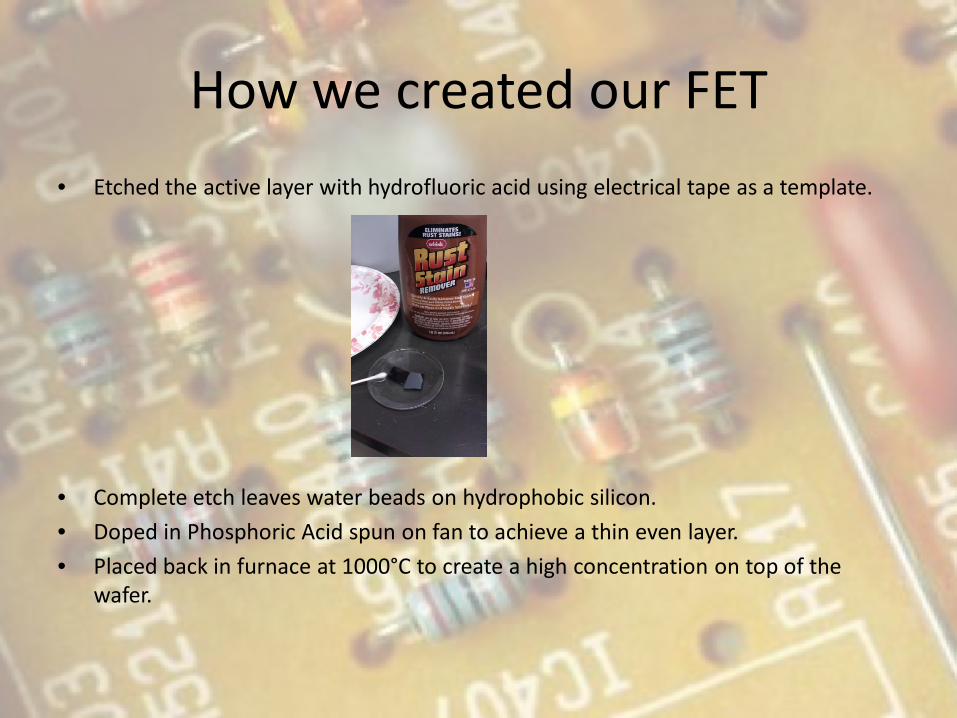
• Etched the active layer with hydrofluoric acid using electrical tape as a template.
• Complete etch leaves water beads on hydrophobic silicon.
• Doped in Phosphoric Acid spun on fan to achieve a thin even layer.
• Placed back in furnace at 1000°C to create a high concentration on top of the wafer.

How we created our FET
• Etched in hydrofluoric acid to remove film (containing contaminants)
• Furnace creates an oxide layer over the P driving it into the wafer.
• Finally using a conductive epoxy we made our points of contact.
What we learned
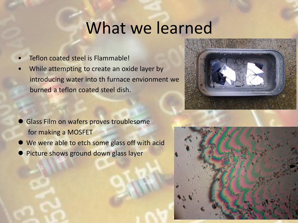
• Teflon coated steel is Flammable! • While attempting to create an oxide layer by introducing water into th furnace envionment we burned a teflon coated steel dish. Glass Film on wafers proves troublesome for making a MOSFET We were able to etch some glass off with acid Picture shows ground down glass layer
What we learned
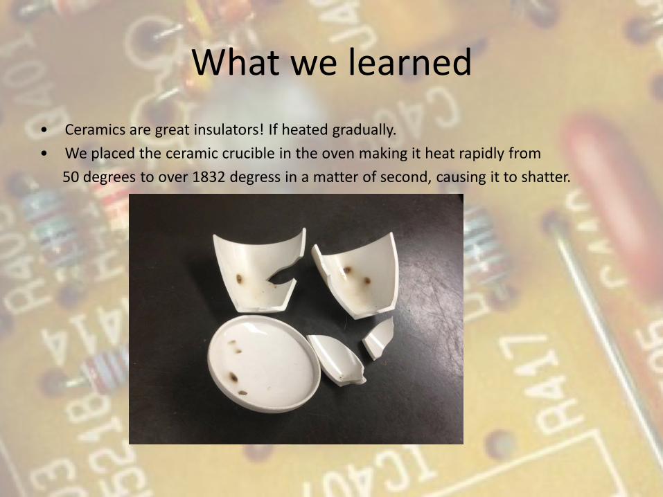
• Ceramics are great insulators! If heated gradually. • We placed the ceramic crucible in the oven making it heat rapidly from 50 degrees to over 1832 degress in a matter of second, causing it to shatter.
What we learned
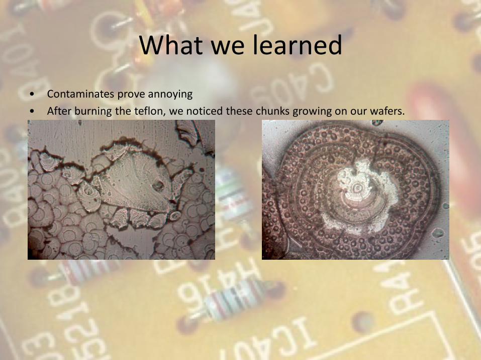
• Contaminates prove annoying • After burning the teflon, we noticed these chunks growing on our wafers.
What we learned
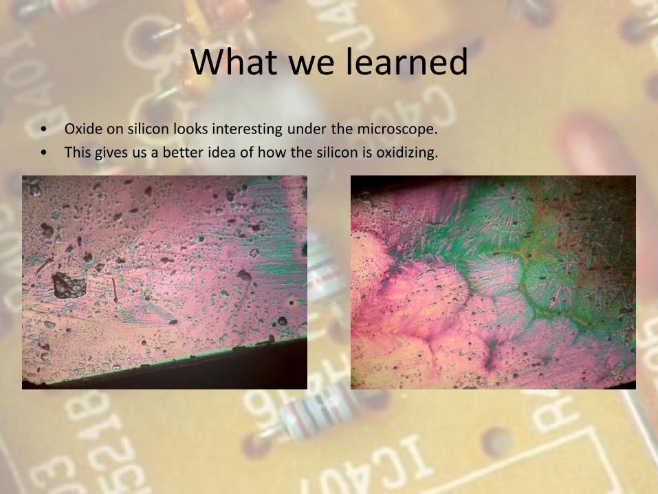
• Oxide on silicon looks interesting under the microscope. • This gives us a better idea of how the silicon is oxidizing.
Results
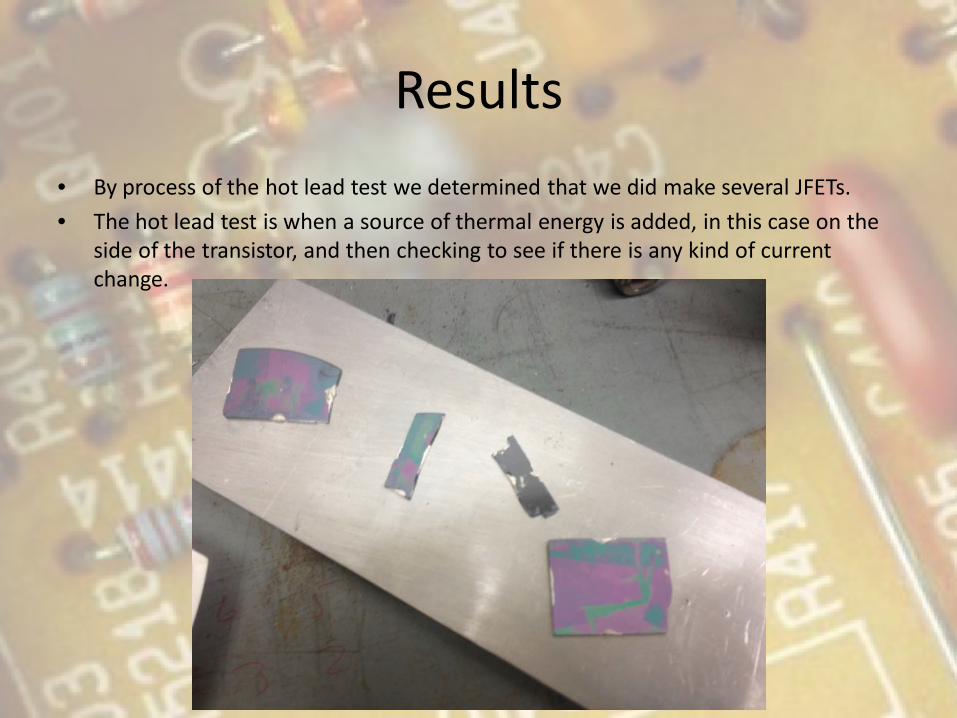
• By process of the hot lead test we determined that we did make several JFETs.
• The hot lead test is when a source of thermal energy is added, in this case on the side of the transistor, and then checking to see if there is any kind of current change.
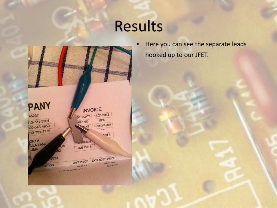
Results • Here you can see the separate leads
hooked up to our JFET.
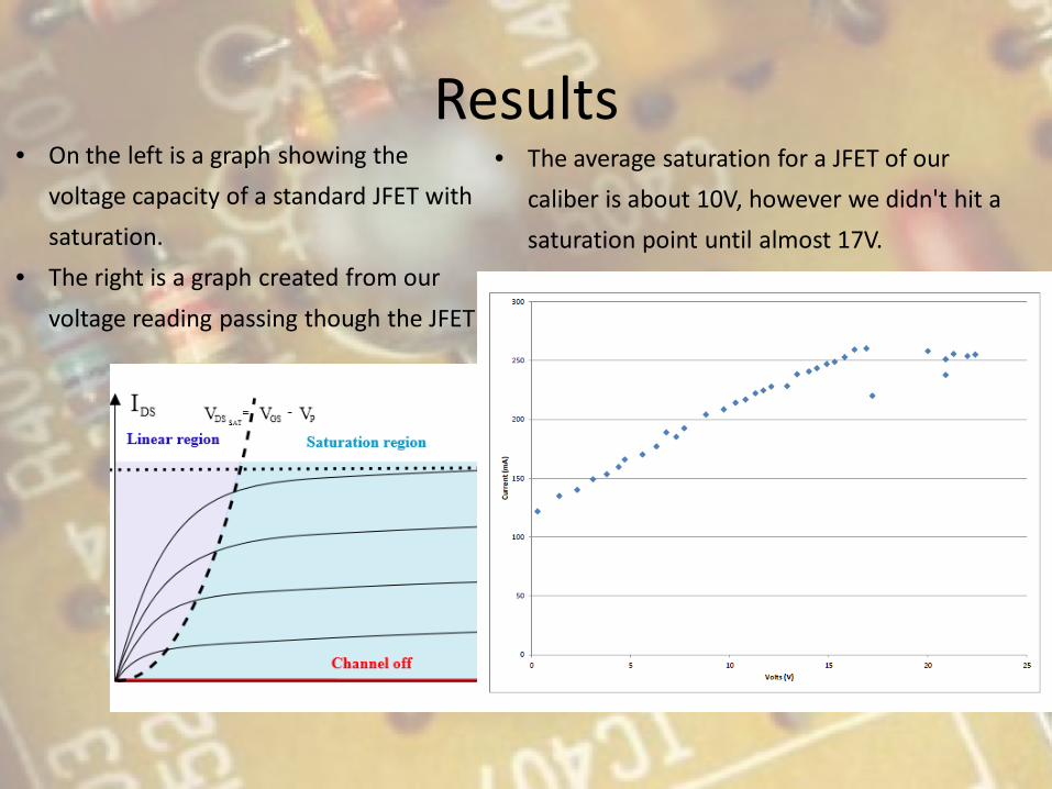
Results • The average saturation for a JFET of our
caliber is about 10V, however we didn't hit a
saturation point until almost 17V.
• On the left is a graph showing the
voltage capacity of a standard JFET with
saturation.
• The right is a graph created from our
voltage reading passing though the JFET
Links
• http://www-ferp.ucsd.edu/najmabadi/CLASS/ECE60L/02-S/NOTES/FET.pdf
• http://www.pbs.org/transistor/science/info/transmodern.html
• http://www.engr.sjsu.edu/kghadiri/EE221/Class_Notes/EE_221_L13_Solid%20state%20Diffusion%20of%20impurities%20in%20Silicon.pdf
• http://www.computerhistory.org/semiconductor/timeline/1957-Zone.html
• http://www.htelabs.com/appnotes/sio2_color_chart_thermal_silicon_dioxide.htm
• http://www.dauniv.ac.in/downloads/Electronic%20Devices/12EDCMOSFETLesson12.pdf