![HITACHI Inspire the Next CV-P85E3 NEW 1,170W£240W 3.5kg ... · HITACHI Inspire the Next CV-P85E3 NEW 1,170W£240W 3.5kg THE HITACHI MOTOR 3.5kg ] eco CV-P85E3 : kadenfan.hitachi.co.jp](https://static.fdocuments.net/doc/165x107/5f2d3c63f04b9d5176570903/hitachi-inspire-the-next-cv-p85e3-new-1170w240w-35kg-hitachi-inspire-the.jpg)
Hitachi 2015 Inspire Innovation ... - FIB SEM User Group 2015 Inspire Innovation Through...
15
Hitachi 2015 Inspire Innovation Through Collaboration Hitachi High Technologies America, Inc. A New Development to Eliminate Artifacts during TEM Sample Preparation in the FIB
-
Upload
hoangkhuong -
Category
Documents
-
view
220 -
download
4
Transcript of Hitachi 2015 Inspire Innovation ... - FIB SEM User Group 2015 Inspire Innovation Through...

Hitachi 2015 Inspire Innovation Through Collaboration Hitachi High Technologies America, Inc.
A New Development to Eliminate Artifacts during TEM Sample Preparation in the FIB

Hitachi 2015
Inspire Innovation Through Collaboration
A Common Problem
(Un)traditional FIB Preparation
• TEM preparation for lift-out has mostly become routine work on FIB-SEM systems recently, with standardized techniques that often are left to automation.
• Several papers addressing ion induced artifacts can be found when preparing lamellas at low kV relating to complex microstructures which often describe complex practices.
• Finalization of a lamella has mostly become: – non-routine – unreliable – Driven by user experience level (varied results, not repeatable)

Hitachi 2015
Inspire Innovation Through Collaboration
A Common Problem
(Un)traditional FIB Preparation
End Point Detection Signal & Scanning System Solution
? Several factors that typically are key to reduce/eliminate ion beam induced artifacts include:
• Scan conditions • Ion species • Sample orientation • Ion beam incident angle • Reproducibility

Hitachi 2015
Inspire Innovation Through Collaboration
Ion Milling Observation Signals
• Several users tend to view while thinning, more often than necessary. • An SEM column with in-column filtering for the separation of signals such as SE and BSE are essential for
identifying the target end point within a sample. • Viewing the lamella while ion milling can be challenging due to high SE signal generation.
BSE - Detector 2kV In-Lens SE Detector 2kV
Simultaneous Observation Cut & See Observation
End Point Detection

Hitachi 2015
Inspire Innovation Through Collaboration
A Common Problem
Ion Species
Damage Ion Species
Solution “The ion beam can be approximated as a
continuous heat source. At shorter times, there are large temporal variations in heating, and at times of less than 10–12 s, the atoms barely have time to interact with each other, and the temperature of the solid is not well defined.” Ref: MRS BULLETIN • VOLUME 32 • MAY 2007 • www/mrs.org/bulletin
Ar-Beam
SEM

Hitachi 2015
Inspire Innovation Through Collaboration
Ion Induced Damage Effects
Ion Species
Damage Gallium Ion
30kV Final Polishing
Gate Poly Si
Si sub
Gate Oxide
65nm NAND Flash

Hitachi 2015
Inspire Innovation Through Collaboration
Gallium Ion
Ion Induced Damage Effects
Ion Species
Damage
5kV Ga Final Polishing
Gate Poly Si
Si sub
Gate Oxide
65nm NAND Flash
5nm
Hitachi 2015
Inspire Innovation Through Collaboration
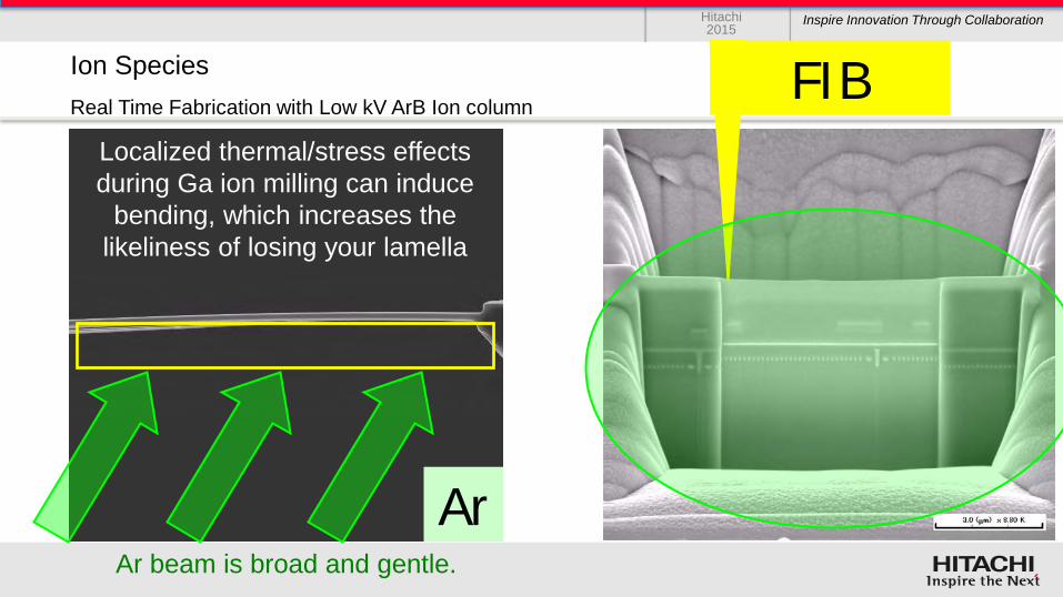
Real Time Fabrication with Low kV ArB Ion column
Ion Species FIB
Ar
Localized thermal/stress effects during Ga ion milling can induce
bending, which increases the likeliness of losing your lamella
Ar beam is broad and gentle.

Hitachi 2015
Inspire Innovation Through Collaboration
Real Time Fabrication with Low kV ArB Ion column
Ion Species FIB
Ar Ar beam is broad and gentle.
Low energy Ar broad ion milling is less destructive and removes
amorphous material left behind by Ga milling

Hitachi 2015
Inspire Innovation Through Collaboration
A Common Problem
Sample Orientation
Curtain Effect Sample Orientation Solution
? Sample orientation with respect to ion incidence angle can influence the planarity of the cross-section face.

Hitachi 2015
Inspire Innovation Through Collaboration
Ion Milling Result for 7-Axis Stage
Anti-Curtaining Function
SIM image of TEM lamella processed by S-axis±15°.
DRAM from Game Machine TEM image (Acc.: 200kV)

Hitachi 2015
Inspire Innovation Through Collaboration
Ion Milling Result for 7-Axis Stage
Anti-Curtaining Function
SIM image of TEM lamella processed by S-axis±15°.
DRAM from Game Machine TEM image (Acc.: 200kV)

Hitachi 2015
Inspire Innovation Through Collaboration
A Common Problem
Enhancing Reproducibility
Throughput Software + Hardware
Productivity, throughput and repeatability are comprised by synergy between:
• User • Application • Hardware*
Ref: http://en.wikipedia.org/wiki/File:Operating_system_placement.svg
Hitachi 2015
Inspire Innovation Through Collaboration
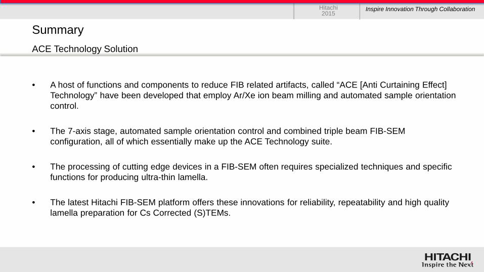
ACE Technology Solution
• A host of functions and components to reduce FIB related artifacts, called “ACE [Anti Curtaining Effect] Technology” have been developed that employ Ar/Xe ion beam milling and automated sample orientation control.
• The 7-axis stage, automated sample orientation control and combined triple beam FIB-SEM configuration, all of which essentially make up the ACE Technology suite.
• The processing of cutting edge devices in a FIB-SEM often requires specialized techniques and specific functions for producing ultra-thin lamella.
• The latest Hitachi FIB-SEM platform offers these innovations for reliability, repeatability and high quality lamella preparation for Cs Corrected (S)TEMs.
Summary