History and prospect of the low-noise CMOS sensor · low-noise CMOS sensors Shoji Kawahito Research...
34
History and prospect of low-noise CMOS sensors Shoji Kawahito Research Institute of Electronics Shizuoka University PIXEL2012 1
Transcript of History and prospect of the low-noise CMOS sensor · low-noise CMOS sensors Shoji Kawahito Research...
History and prospect of low-noise CMOS sensors
Shoji Kawahito Research Institute of Electronics
Shizuoka University
PIXEL2012 1

Typical CIS Architecture
2
- Charge-transfer-type active pixel with pinned photodiode - Column CDS (Correlated double sampling) Amplifier (if necessary) - High-speed A/D conversion Using 1-D parallel operation - High-speed low-noise digital signaling like LVDS (low-voltage differential signaling)
V.
Column CDS (Amp.) & ADC

Low Noise CMOS Image Sensors: Design Challenges
1. Low Noise (<2e-)
2. Low Noise at High Pixel Rate (= frame rate x # of pixels)
3. Low Noise and High Intrascene Dynamic Range
4. Sub-electron Noise
PIXEL2012 3

Low Noise CMOS Image Sensors
1. Low Noise (<2e-)
2. Low Noise at High Pixel Rate (= frame rate x # of pixels)
3. Low Noise and High Intrascene Dynamic Range
4. Sub-electron Noise
PIXEL2012 4

Dark Noise in CMOS Image Sensors 1. Temporal Random Noise - Dark Current (Shot Noise) - Reset or kTC Noise - Amplifier’s noise (thermal and 1/f noise) - Row (Horizontal) Noise 2. Fixed-Pattern Noise - Pixel Source Follower’s - Column Readout Circuit’s (Vertical FPN) - Dark Current
PIXEL2012 5

Active Pixel Sensors 3Tr. APS
・Used in end of 90’s as a first cell-phone camera. ・kTC noise is NOT cancelled. ・Large dark current ・Conversion gain is determined by PD Cap.
・kTC noise is cancelled. ・Low dark current due to pinned photodiode ・High conversion gain due to small floating diffusion capacitance.
4Tr. APS (In-pixel charge transfer) Chamberlain, IEEE-JSSC ’69 Lee et al., E. Fossum, Workshop, CCD &AIS, 1995.

Readout Operation in CIS
Vreset
Vsignal
Vreset
Ri
TXi
VFD
Vsignal Vreset
VFD
CDS (Correlated Double Sampling)
T1H
FDsresetsignalout CQVVV /∝−=
- Fixed Pattern Noise Cancelling - kTC(Reset) Noise Cancelling
7

Thermal noise and 1/f noise in CMOS image sensors
log f
Pow
er sp
ectr
um d
ensit
y (lo
g)
Thermal noise (Sn=4kTR)
1/f noise (Sn=Nf/f)

Circuits’ Noise in CMOS Image Sensors
9
Signal Chain
PIXEL2012
2 2 2 2 2, , , , ,
2 2, ,
2
1 ( )
( 1)
n in n SF n NC n OB n ADC
n SF n C C
C
N N
N
V V V V
V V
GV
G
= + + +
≅ + >>
Input-Referred Noise (if GSF=1)
Gain of column amplifier greatly reduces wideband circuit noise.
Column Noise Canceller (Amp.)
BW~100MHz BW~1MHz
GSF

Column-Parallel Correlated Multiple Sampling
( ) ( )( )1
M
OUT R Si
V V i V i=
= −∑10 M-time Sampling has a gain of M Noise Reduction
Column

Noise Reduction Effect of Correlated Multiple Sampling
Input Referred Noise
2 2, ,2
, ,1/ 2n th n OB
n in n f
V VV V
M M≅ + +
log M
,log n inV
1M
1M
2,1/ :n fV 1/f Noise of S.F.
for M=1. 2
, :n thV Thermal Noise of S.F. for M=1.
2, :n OBV Noise of wideband
output buffer Dominant Noise Source
Pixel
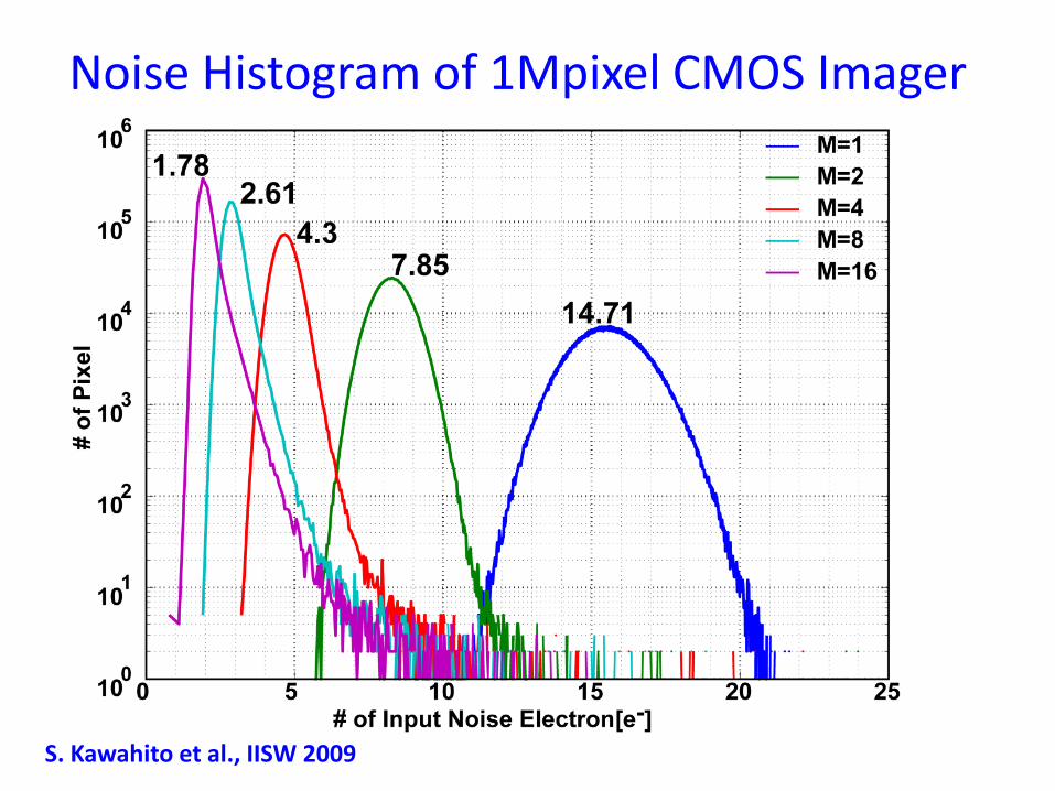
Noise Histogram of 1Mpixel CMOS Imager
S. Kawahito et al., IISW 2009

Low Noise CMOS Image Sensors
1. Low Noise (<2e-)
2. Low Noise at High Pixel Rate (= frame rate x # of pixels)
3. Low Noise and High Intrascene Dynamic Range
4. Sub-electron Noise
PIXEL2012 13

CIS Using Column ADC
14
- High-speed A/D conversion Using 1-D Parallel Processing - High-speed low-noise digital signaling like LVDS (low-voltage differential signaling) is used. -Digital H. Read is 10times faster than Analog. (Analog : several 10MHz, Digital: several 100MHz)
V.
Column CDS (Amp.) & ADC

• Measure the time when VRAMP equals to Vin using a counter. • Basic Elements: Comparator and counter (or register) • N-bit conversion requires 2N clocks.
Single-Slope ADC
15
Vin
VRAMP
Count
Operation
10b single-slope: Toshiba (ISSCC ’00)

13b Column-Parallel Cyclic ADC
Symplest Cyclic ADC (One Amp., Two Comparators, 3 Caps) M-1 Cycles for M bits Low Noise (4.9e-, gain=unity, 61uV/e-)
J. H. Park, S. Kawahito et al., ISSCC ’09 16

Operation of Cyclic ADC
17
1bit ADC {0,1}
Amplified by 2 and subtract 1-bit DAC out (0,R)
1 12i i iX X D R− −= − ×
N cycles for N bits
Basic Operation: Actual Implementation:3-state {-1,0,1} sub-ADC is used for relaxing comparator precision (N-1 cycles for N bits)
R

Implemented CMOS Imager
0.18μm CIS Process
4-Tr. Pinned photodiode
Pixel Size : 5.6μm X 5.6μm
ADC Resolution : 13b
Frame rate : 340 fps
18

Noise Versus Frame Rage
Low ADC Noise (2.5e-): Constant up to 390fps Low total noise without gaing (4.9e-
rms) 19

Two-stage Column-parallel Cyclic ADC
20
High-speed with pipeline and parallel operation Low-power and small area design for 2nd stage cyclic ADC exploiting
amplifier function of cyclic ADC
1st stage cyclic ADC 2nd stage cyclic ADC
Vin1 Vout1 Vin2
Data out (Upper 4-bit) Data out (Lower 8-bit)
ΦSA ΦSB
VIN×24 VIN
4 cycles 8 cycles

Noise – Pixel Rate of Digital CISs
33M, 120fps CIS
17.7M, 120fps CIS

Low Noise CMOS Image Sensors
1. Low Noise (<2e-)
2. Low Noise at High Pixel Rate (= frame rate x # of pixels)
3. Low Noise and High Intrascene Dynamic Range
4. Sub-electron Noise
PIXEL2012 22
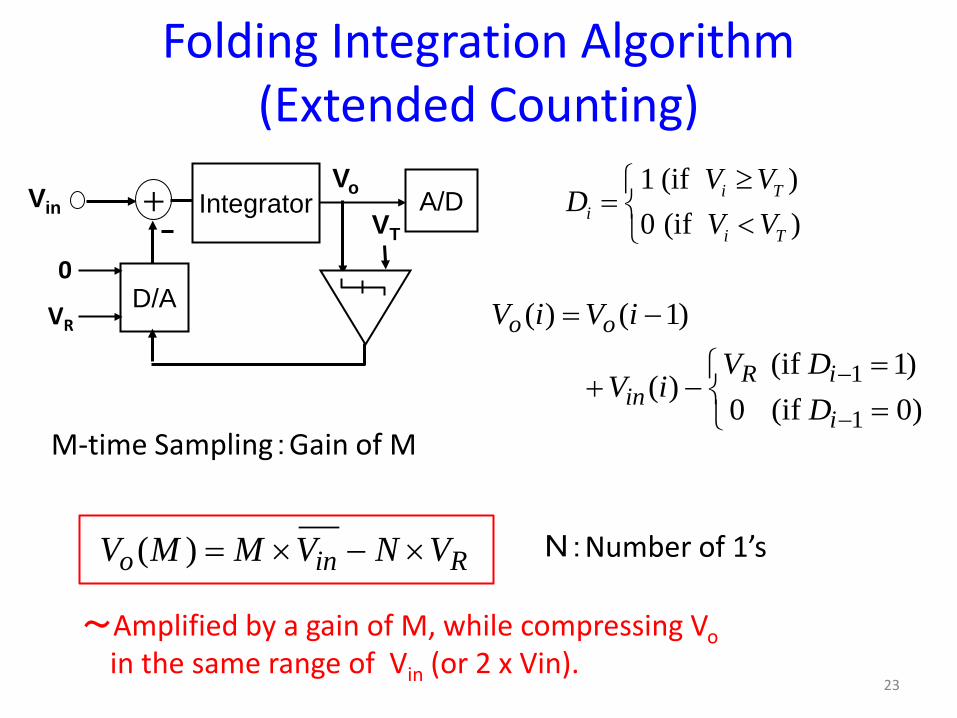
Folding Integration Algorithm (Extended Counting)
+ Integrator VT
D/A
Vin
0
VR
A/D
1
1
( ) ( 1) (if 1)
( )0 (if 0)
o o
R iin
i
V i V iV D
V iD
−
−
= −
=+ − =
1 (if )0 (if )
i Ti
i T
V VD
V V≥
= <
Vo
( )o in RV M M V N V= × − ×
M-time Sampling:Gain of M
~Amplified by a gain of M, while compressing Vo
in the same range of Vin (or 2 x Vin).
N:Number of 1’s
23

24
Transfer Curve of the Folding-Integration ADC (M=16)
• Output signal is compressed into 1 to 2V by folding operation. • # of counts is used for coarse ADC. Cyclic ADC is used for the analog output. • Folding integration is also known as extended counting*.
Compress Expand
[*Jansson, IEEE Transactions on circuits and systems, 1995]

Block Diagram of the Folding Integration/Cyclic ADC
25
・The total resolution is M+N-1 [bits], very high gray-scale resolution (18b). ・ The analog core is used for both the folding-integration and cyclic ADCs. (No additional analog circuits than that for cyclic ADC)
Folding Integration ADC(M=1b - 7b)
Cyclic ADC(N=13b)

26
Noise Histogram of 1Mpixel CIS Noise [electron]
0.1 1 10 100
Num
ber o
f Pix
els

Linearity of Photo Response
27
82dB

EM-CCD (Gain:X800, Cooling:-10℃, 4fps) HS-CMOS (Gain:X768, Cooling:10℃, 4fps)
28
Illumination :0.005lx

WDR Verification of HSC09 compare with EM-CCD Dynamic Range Comparison
(EM-CCD) (HS-CMOS, γ=1.65, DR=82dB)
29

Low Light Level Image (1.3M, 7.1um, @30fps, 1.2e-)
0.01 [lx] 0.001 [lx]
0.1 [lx] 300 [lx]
30

Low Noise CMOS Image Sensors
1. Low Noise (<2e-)
2. Low Noise at High Pixel Rate (= frame rate x # of pixels)
3. Low Noise and High Intrascene Dynamic Range
4. Sub-electron Noise
PIXEL2012 31

Reports on Low-Noise CISs (<1.1e-) Technique Used Noise Conversion
Gain [µV/e-] Reference
[µV] [e-]
Column Amplifier (G=32), Single-Slope ADC (SSADC) n. a. 0.8 n.a.
(2.1DN/e-) IISW 2007
Multiple Sampling, Folding Integration/ Cyclic ADC 65µV 0.95 67µV/e- ISSCC 2011,
JSSC (Jan.,2012)
Pseudo Multiple Sampling with SSADC 121µV 1.1 110µV/e- ISSCC 2010
PMOS Common-Source Pixel Amp. 260µV 0.86 300µV/e- ISSCC 2010
Buried Channel nMOS S. F. Multiple Sampling with SSADC 32µV 0.7 45µV/e- ISSCC 2012
nMOS S. F. with Switched Biasing n. a. 0.5 n. a. www.caeleste.com, 2011
PIXEL2012 32
Low 1/f Noise Pixel + Multiple Sampling Column ADC

How to realize 0.1e- Noise
Not: Effective Trap Density[cm-2] Presently, 107 ~108cm-2 Highest Conversion gain reported ~300e-
Noi
se [e
-]
2
2
1 fotnf
ox G
Nq NSC A f f
= =
1/f Noise Spectrum
c SFFD
qG GC
=
・Low 1/f Noise Transistor :Small Not ・High Conversion Gain Charge Detector (>1000µV/e-) (extremely small capacitance of <0.1fF)

Summary • Pixel : Charge transfer active pixel with pinned
photodiode (Low dark current, kTC noise canceling and high conversion gain)
• Low circuit noise : High gain column readout circuits (using multiple sampling and ADC)
• Low noise at high pixel rate : column ADC is the key
• Low noise and wide dynamic range : enabled by column readout circuits (Advantage of CMOS)
• Sub-electron noise imager: low 1/f noise pixel amplifier (further reduction: high conversion gain)
PIXEL2012 34


![[PPT] Noise and Matching in CMOS (Analog) Circuits](https://static.fdocuments.net/doc/165x107/55cf932b550346f57b9c555d/ppt-noise-and-matching-in-cmos-analog-circuits.jpg)