HILONC V2 DEVELOPMENT KIT APPLICATION...
24
HILONC V2 DEVELOPMENT KIT APPLICATION NOTE ~ Freedom of speech for smart machines ~
Transcript of HILONC V2 DEVELOPMENT KIT APPLICATION...
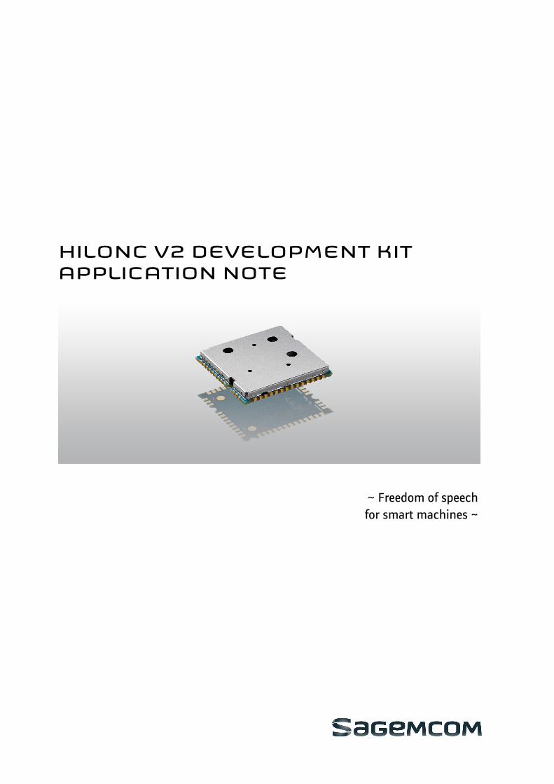
HILONC V2 DEVELOPMENT KIT
APPLICATION NOTE
~ Freedom of speech
for smart machines ~
Note d’étude / Technical document :
URD1– OTL 5665.3– 007 / 72 399 Edition 01 HiLoNC V2 Development Kit Application Note
25/10/2010 - Page 2 / 23
FICHE RECAPITULATIVE / SUMMARY SHEET
Ed Date
Date
Référence
Reference
Pages modifiées / Changed
pages
Observations
Comments
1 25/10/2010 URD1– OTL 5665.3– 007 / 72 399 Edition 01
All Création du document Document creation
2
3
4
5
6
7
Note d’étude / Technical document :
URD1– OTL 5665.3– 007 / 72 399 Edition 01 HiLoNC V2 Development Kit Application Note
25/10/2010 - Page 3 / 23
SOMMAIRE / CONTENTS
1. SCOPE .......................................................................................................................................................4
1.1. Introduction..............................................................................................................................................4
1.2. Reference................................................................................................................................................4
1.3. Terms and abbreviation...........................................................................................................................4
2. PRODUCT OVERVIEW..............................................................................................................................5
2.1. Key features ............................................................................................................................................5
2.2. Functional diagram..................................................................................................................................5
2.3. Interfaces location ...................................................................................................................................7
2.3.1. Connectors.......................................................................................................................................7
2.3.2. Test points........................................................................................................................................8
2.3.3. Switches...........................................................................................................................................9
2.3.4. Jumpers .........................................................................................................................................10
2.3.5. Miscellaneous ................................................................................................................................12
3. GETTING STARTED WITH THE DEVELOPMENT KIT ..........................................................................13
3.1. Power Supply not connected.................................................................................................................13
3.2. Switch on the Development Kit .............................................................................................................13
3.3. Communication with the module ...........................................................................................................13
4. HILONC V2 DEVELOPMENT KIT INTERFACE.......................................................................................15
4.1. Test Points interface..............................................................................................................................15
4.2. SIM interface .........................................................................................................................................16
4.2.1. SIM IC ............................................................................................................................................16
4.2.2. SIM CARD......................................................................................................................................16
4.3. Serial Interface ......................................................................................................................................16
4.3.1. UART 1 ..........................................................................................................................................16
4.3.2. UART 0 ..........................................................................................................................................17
4.4. GPIOs interface.....................................................................................................................................17
4.5. Analog audio interface...........................................................................................................................18
4.5.1. Functional diagram.........................................................................................................................18
4.6. 51-pins module interface.......................................................................................................................19
4.7. Miscellneous..........................................................................................................................................21
4.7.1. PWMs ............................................................................................................................................21
4.7.2. BACKUP ........................................................................................................................................21
4.7.3. ADC................................................................................................................................................21
4.7.4. GSM Antenna.................................................................................................................................22
4.7.5. Auto power-on................................................................................................................................22
4.7.6. Hardware reset...............................................................................................................................22
4.8. Overview of jumpers..............................................................................................................................22
4.9. Overview of Switchers...........................................................................................................................23
Note d’étude / Technical document :
URD1– OTL 5665.3– 007 / 72 399 Edition 01 HiLoNC V2 Development Kit Application Note
25/10/2010 - Page 4 / 23
1. SCOPE
1.1. Introduction The object of the document is to describe the interfaces and pin identifications of the Development Kit to test the HiLoNC V2 module in operating mode.
1.2. Reference � HiLoNC V2 Development Kit Schematic � HiLoNC V2 Specification: 5635.1 005 70086 ed 04 - HiLoNC V2 technical specification.doc � HiLoNC V2 Application Note: 5635.1 007 70230 ed 01 - HiLoNC V2 application note.doc � Temperature sensor “ADT7302” specification: ADT7302.pdf � Inertial sensor LIS3LV02DQ specification: LIS3LV02DQ.pdf � URD1 - OTL 5625.1 - 010 - N°69846 - DEMOBOARD MO300 APPLICATION NOTE - ED01.doc
1.3. Terms and abbreviation
ADC Analog to Digital Converter CTS Clear To Send DAC Digital to Analog Converter DAI Digital Audio Interface DCS Digital Communications System DSR Data Set Ready DTR Data Terminal Ready ESD Electrostatic Discharge GSM Global System for Mobile communication GPRS General Packet Radio Services I/O Input / Output Kbps Kbits per second LED Light Emitting Diode Mbps Mbits per second PCB Printed Circuit Board PSU Power supply unit RF Radio Frequency RI Ring Indication RTS Ready To Send RX Reception SIM Subscriber Identification Module TX Transmission UART Universal Asynchronous Receiver and Transmitter
Note d’étude / Technical document :
URD1– OTL 5665.3– 007 / 72 399 Edition 01 HiLoNC V2 Development Kit Application Note
25/10/2010 - Page 5 / 23
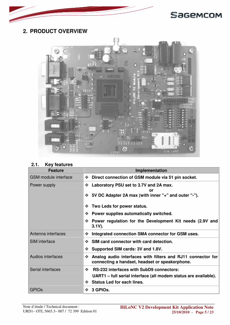
2. PRODUCT OVERVIEW
2.1. Key features
Feature Implementation
GSM module interface � Direct connection of GSM module via 51 pin socket.
Power supply � Laboratory PSU set to 3.7V and 2A max. or
� 5V DC Adapter 2A max (with inner "+" and outer "-").
� Two Leds for power status.
� Power supplies automatically switched.
� Power regulation for the Development Kit needs (2.9V and 3.1V).
Antenna interfaces � Integrated connection SMA connector for GSM uses.
SIM interface � SIM card connector with card detection.
� Supported SIM cards: 3V and 1.8V.
Audios interfaces � Analog audio interfaces with filters and RJ11 connector for connecting a handset, headset or speakerphone.
Serial interfaces � RS-232 interfaces with SubD9 connectors:
UART1 – full serial interface (all modem status are available).
� Status Led for each lines.
GPIOs � 3 GPIOs.
Note d’étude / Technical document :
URD1– OTL 5665.3– 007 / 72 399 Edition 01 HiLoNC V2 Development Kit Application Note
25/10/2010 - Page 6 / 23
� Able to be switched in/out and pull-up/pull-down resistors.
� Status Led for each I/Os.
ADC interface � One analog input (0 to 1.8V).
Protections � ESD and EMC protections on each pin headers and connectors of the Development Kit.
Physical characteristics � Size : 168mm x 118mm x 30mm
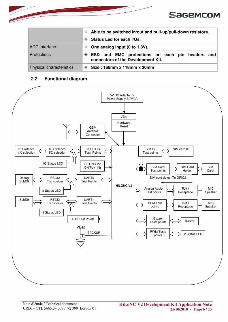
2.2. Functional diagram
03 Switches 1/0 selection
03 Switches I/O selection
03 GPIO’s Test Points
03 Status LED
Debug SubD9
RS232 Transceiver
UART0 Test Points
2 Status LED
SubD9 RS232 Transceiver
UART1 Test Points
8 Status LED
GSM Antenna
Connector
5V DC Adapter or Power Supply 3.7V/2A
VBat
Hardware Reset
SIM IC Test points
SIM card IC
SIM Card Test points
SIM Card Holder
SIM Card
Analog Audio Test points
RJ11 Receptade
MIC Speaker
PCM Test points
RJ11 Receptade
MIC Speaker
HILONC V2
HILONC V2 ON(Pok_IN)
SIM card detect To GPIO2
Buzzer Tests points Buzzer ADC Test Points
PWM Tests points 2 Status LED
VBat BACKUP

Note d’étude / Technical document :
URD1– OTL 5665.3– 007 / 72 399 Edition 01 HiLoNC V2 Development Kit Application Note
25/10/2010 - Page 7 / 23
2.3. Interfaces location 2.3.1. Connectors
Location Connector’s Type Function
MX104 51 pins socket Module interface
P202 UART1 P402
Sub-D 9 Connector UART0 (Debug)
P501 P502
RJ11 Receptacle Analog audio
P101 SMA Connector 50 Ohms Antenna GSM
TB801
TB802
Laboratory power supply receptacle
Ø 4mm Power supply 1
P801 Mini DC jack (+ inner, - outer) Ø 2.5mm
Power supply 2
P601 Sim card holder SIM
Note d’étude / Technical document :
URD1– OTL 5665.3– 007 / 72 399 Edition 01 HiLoNC V2 Development Kit Application Note
25/10/2010 - Page 8 / 23
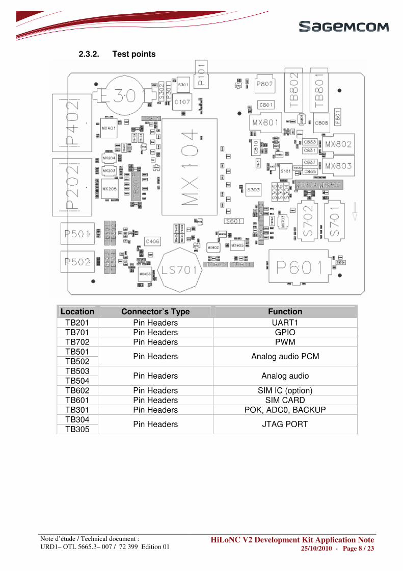
2.3.2. Test points
Location Connector’s Type Function
TB201 Pin Headers UART1 TB701 Pin Headers GPIO TB702 Pin Headers PWM TB501 TB502
Pin Headers Analog audio PCM
TB503 TB504
Pin Headers Analog audio
TB602 Pin Headers SIM IC (option) TB601 Pin Headers SIM CARD TB301 Pin Headers POK, ADC0, BACKUP TB304 TB305
Pin Headers JTAG PORT
Note d’étude / Technical document :
URD1– OTL 5665.3– 007 / 72 399 Edition 01 HiLoNC V2 Development Kit Application Note
25/10/2010 - Page 9 / 23
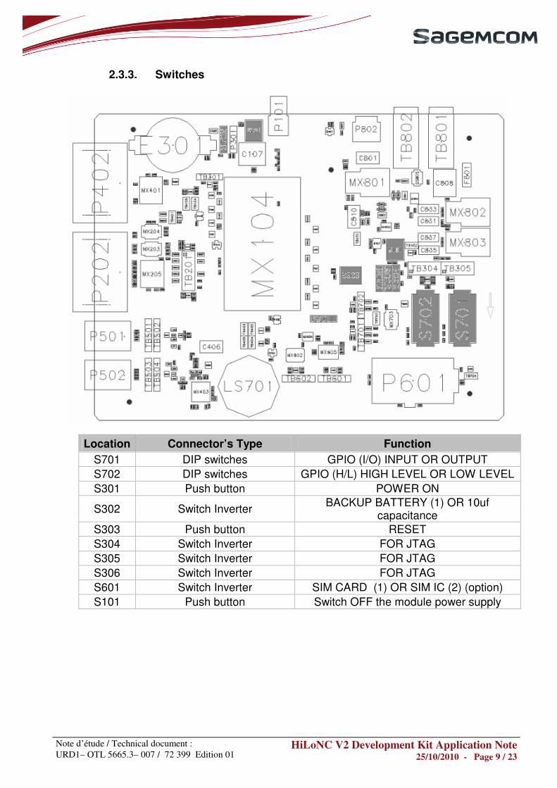
2.3.3. Switches
Location Connector’s Type Function
S701 DIP switches GPIO (I/O) INPUT OR OUTPUT S702 DIP switches GPIO (H/L) HIGH LEVEL OR LOW LEVEL S301 Push button POWER ON
S302 Switch Inverter BACKUP BATTERY (1) OR 10uf capacitance
S303 Push button RESET S304 Switch Inverter FOR JTAG S305 Switch Inverter FOR JTAG S306 Switch Inverter FOR JTAG S601 Switch Inverter SIM CARD (1) OR SIM IC (2) (option) S101 Push button Switch OFF the module power supply
Note d’étude / Technical document :
URD1– OTL 5665.3– 007 / 72 399 Edition 01 HiLoNC V2 Development Kit Application Note
25/10/2010 - Page 10 / 23
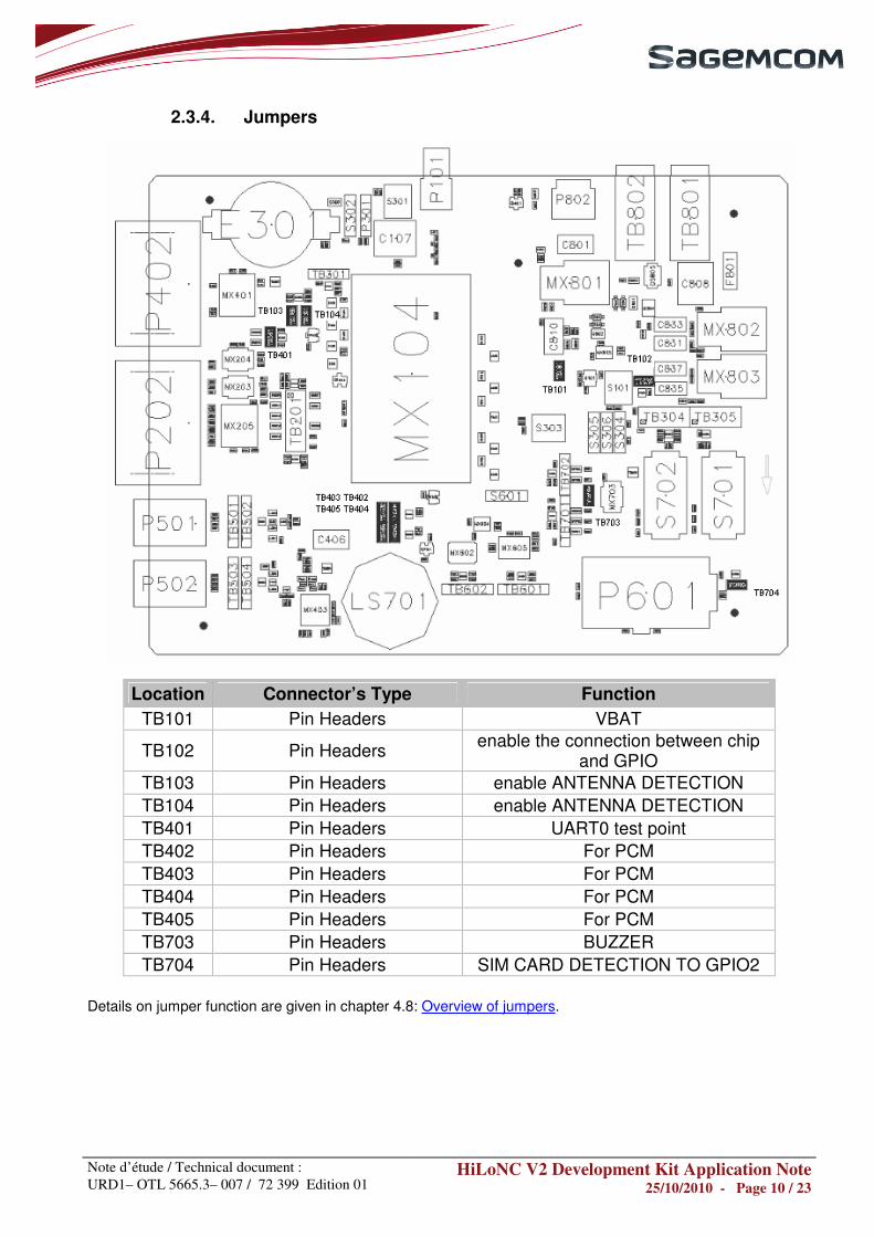
2.3.4. Jumpers
Location Connector’s Type Function
TB101 Pin Headers VBAT
TB102 Pin Headers enable the connection between chip and GPIO
TB103 Pin Headers enable ANTENNA DETECTION TB104 Pin Headers enable ANTENNA DETECTION TB401 Pin Headers UART0 test point TB402 Pin Headers For PCM TB403 Pin Headers For PCM TB404 Pin Headers For PCM TB405 Pin Headers For PCM TB703 Pin Headers BUZZER TB704 Pin Headers SIM CARD DETECTION TO GPIO2
Details on jumper function are given in chapter 4.8: Overview of jumpers.

Note d’étude / Technical document :
URD1– OTL 5665.3– 007 / 72 399 Edition 01 HiLoNC V2 Development Kit Application Note
25/10/2010 - Page 11 / 23
Note d’étude / Technical document :
URD1– OTL 5665.3– 007 / 72 399 Edition 01 HiLoNC V2 Development Kit Application Note
25/10/2010 - Page 12 / 23
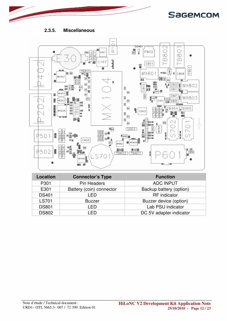
2.3.5. Miscellaneous
Location Connector’s Type Function
P301 Pin Headers ADC INPUT E301 Battery (coin) connector Backup battery (option)
DS401 LED RF indicator LS701 Buzzer Buzzer device (option) DS801 LED Lab PSU indicator DS802 LED DC 5V adapter indicator
Note d’étude / Technical document :
URD1– OTL 5665.3– 007 / 72 399 Edition 01 HiLoNC V2 Development Kit Application Note
25/10/2010 - Page 13 / 23
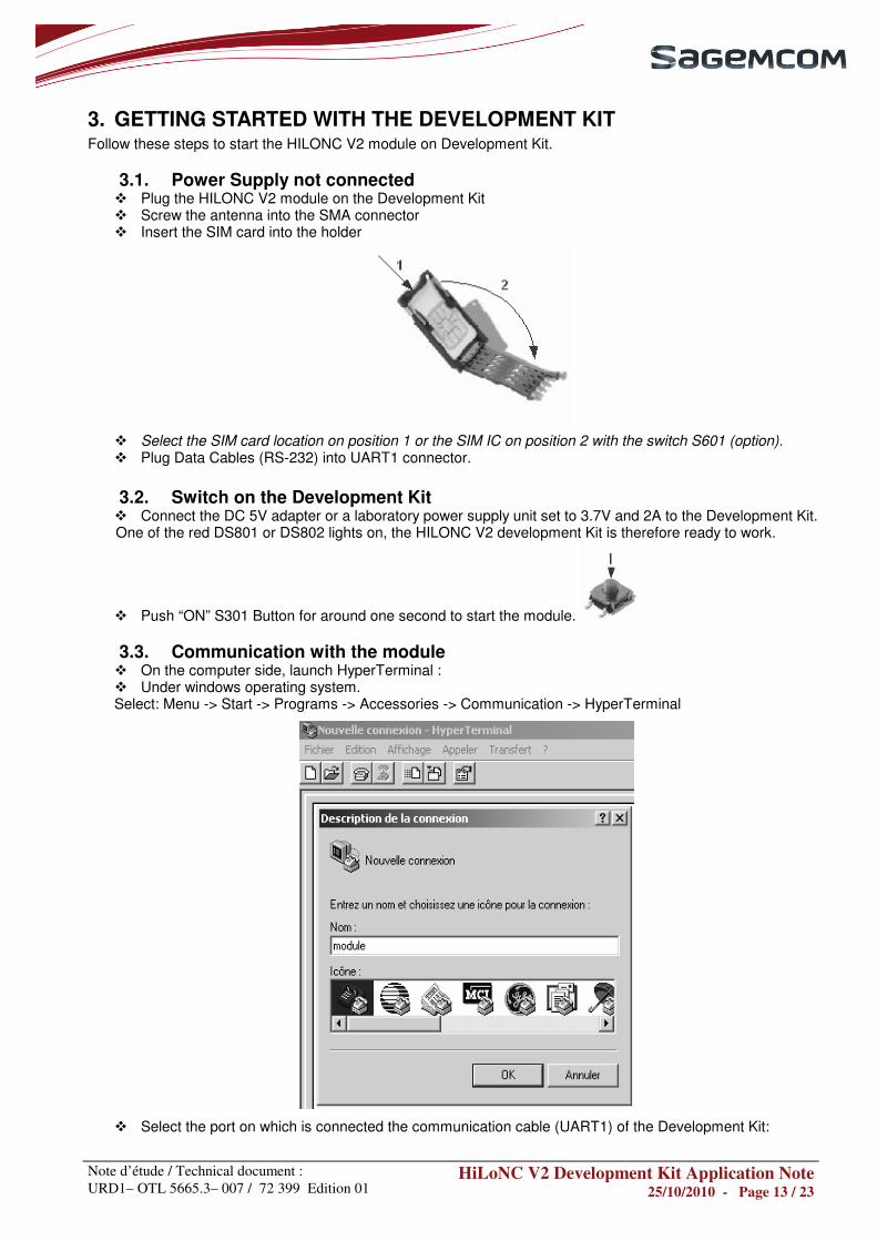
3. GETTING STARTED WITH THE DEVELOPMENT KIT Follow these steps to start the HILONC V2 module on Development Kit.
3.1. Power Supply not connected � Plug the HILONC V2 module on the Development Kit � Screw the antenna into the SMA connector � Insert the SIM card into the holder
� Select the SIM card location on position 1 or the SIM IC on position 2 with the switch S601 (option). � Plug Data Cables (RS-232) into UART1 connector.
3.2. Switch on the Development Kit � Connect the DC 5V adapter or a laboratory power supply unit set to 3.7V and 2A to the Development Kit. One of the red DS801 or DS802 lights on, the HILONC V2 development Kit is therefore ready to work.
� Push “ON” S301 Button for around one second to start the module. 3.3. Communication with the module � On the computer side, launch HyperTerminal : � Under windows operating system. Select: Menu -> Start -> Programs -> Accessories -> Communication -> HyperTerminal
� Select the port on which is connected the communication cable (UART1) of the Development Kit:
Note d’étude / Technical document :
URD1– OTL 5665.3– 007 / 72 399 Edition 01 HiLoNC V2 Development Kit Application Note
25/10/2010 - Page 14 / 23
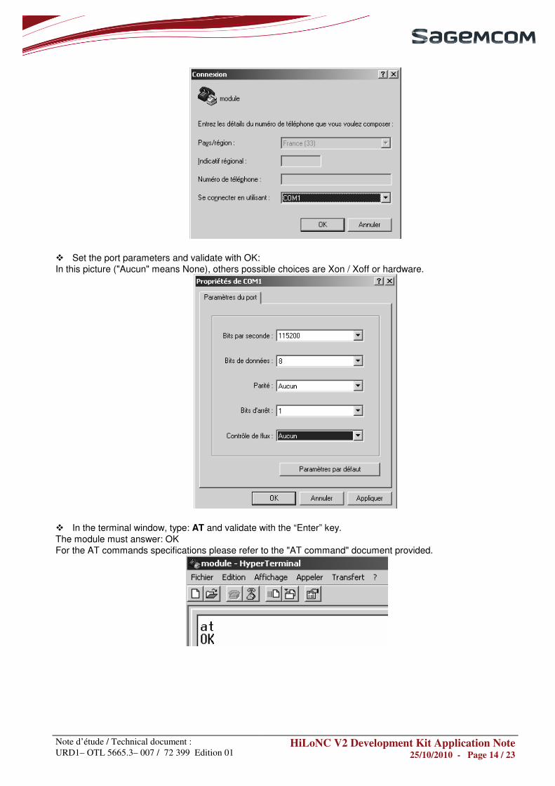
� Set the port parameters and validate with OK: In this picture ("Aucun" means None), others possible choices are Xon / Xoff or hardware.
� In the terminal window, type: AT and validate with the “Enter” key. The module must answer: OK For the AT commands specifications please refer to the "AT command" document provided.

Note d’étude / Technical document :
URD1– OTL 5665.3– 007 / 72 399 Edition 01 HiLoNC V2 Development Kit Application Note
25/10/2010 - Page 15 / 23
4. HILONC V2 DEVELOPMENT KIT INTERFACE
4.1. Test Points interface
All signals provided by the module are directly connected to pin headers and divided by interface. For signals features please refer to: “URD1 5635.1 005 70086 - HiLoNC V2 technical specification “ document provided.
INTERFACE PINNING
UART 1
UART 0
GPIO
Analog audio_PCM
Analog audio
SIM IC
PWM
Note d’étude / Technical document :
URD1– OTL 5665.3– 007 / 72 399 Edition 01 HiLoNC V2 Development Kit Application Note
25/10/2010 - Page 16 / 23
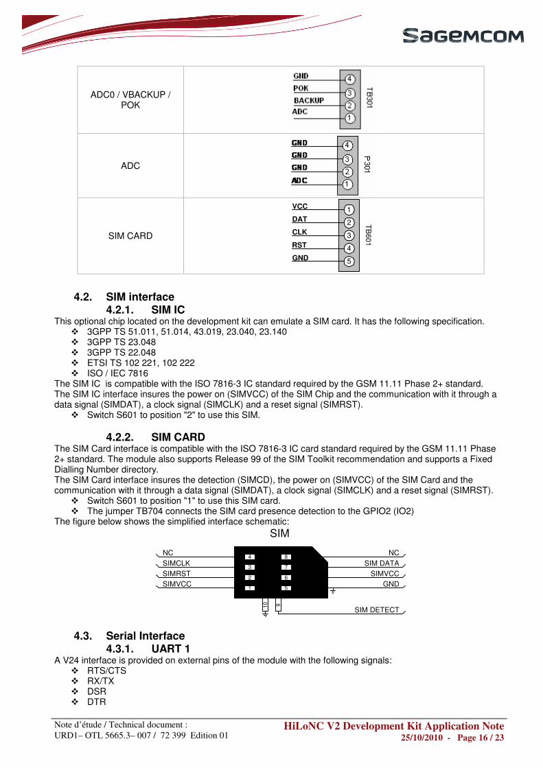
ADC0 / VBACKUP / POK
ADC
SIM CARD
GND
RST
CLK
DAT
VCC 1
2
3
4
5
TB
601
4.2. SIM interface 4.2.1. SIM IC
This optional chip located on the development kit can emulate a SIM card. It has the following specification. � 3GPP TS 51.011, 51.014, 43.019, 23.040, 23.140 � 3GPP TS 23.048 � 3GPP TS 22.048 � ETSI TS 102 221, 102 222 � ISO / IEC 7816
The SIM IC is compatible with the ISO 7816-3 IC standard required by the GSM 11.11 Phase 2+ standard. The SIM IC interface insures the power on (SIMVCC) of the SIM Chip and the communication with it through a data signal (SIMDAT), a clock signal (SIMCLK) and a reset signal (SIMRST).
� Switch S601 to position "2" to use this SIM.
4.2.2. SIM CARD The SIM Card interface is compatible with the ISO 7816-3 IC card standard required by the GSM 11.11 Phase 2+ standard. The module also supports Release 99 of the SIM Toolkit recommendation and supports a Fixed Dialling Number directory. The SIM Card interface insures the detection (SIMCD), the power on (SIMVCC) of the SIM Card and the communication with it through a data signal (SIMDAT), a clock signal (SIMCLK) and a reset signal (SIMRST).
� Switch S601 to position "1" to use this SIM card. � The jumper TB704 connects the SIM card presence detection to the GPIO2 (IO2)
The figure below shows the simplified interface schematic:
8
6
7
5
4
2
3
1
10 9
NCSIMCLKSIMRSTSIMVCC
NCSIM DATA
SIMVCCGND
SIM DETECT
SIM
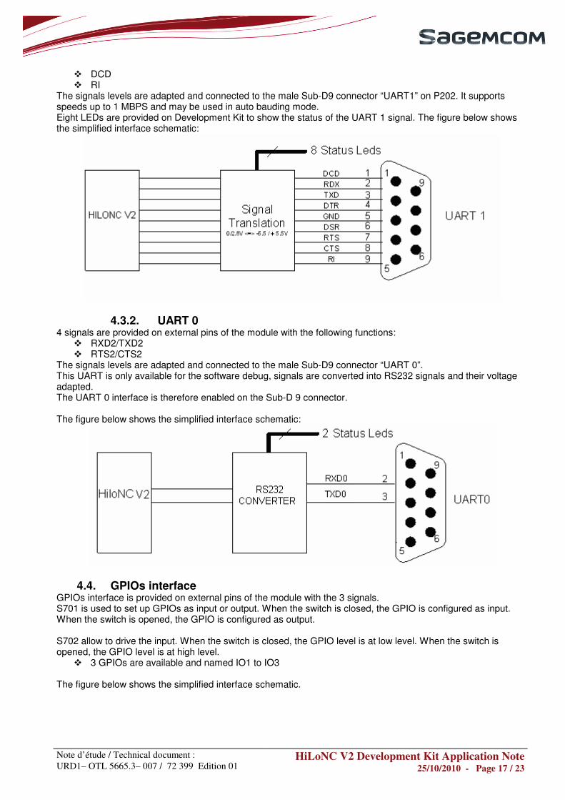
4.3. Serial Interface 4.3.1. UART 1
A V24 interface is provided on external pins of the module with the following signals: � RTS/CTS � RX/TX � DSR � DTR
Note d’étude / Technical document :
URD1– OTL 5665.3– 007 / 72 399 Edition 01 HiLoNC V2 Development Kit Application Note
25/10/2010 - Page 17 / 23
� DCD � RI
The signals levels are adapted and connected to the male Sub-D9 connector “UART1” on P202. It supports speeds up to 1 MBPS and may be used in auto bauding mode. Eight LEDs are provided on Development Kit to show the status of the UART 1 signal. The figure below shows the simplified interface schematic:
4.3.2. UART 0 4 signals are provided on external pins of the module with the following functions:
� RXD2/TXD2 � RTS2/CTS2
The signals levels are adapted and connected to the male Sub-D9 connector “UART 0”. This UART is only available for the software debug, signals are converted into RS232 signals and their voltage adapted. The UART 0 interface is therefore enabled on the Sub-D 9 connector. The figure below shows the simplified interface schematic:
4.4. GPIOs interface GPIOs interface is provided on external pins of the module with the 3 signals. S701 is used to set up GPIOs as input or output. When the switch is closed, the GPIO is configured as input. When the switch is opened, the GPIO is configured as output. S702 allow to drive the input. When the switch is closed, the GPIO level is at low level. When the switch is opened, the GPIO level is at high level.
� 3 GPIOs are available and named IO1 to IO3 The figure below shows the simplified interface schematic.
Note d’étude / Technical document :
URD1– OTL 5665.3– 007 / 72 399 Edition 01 HiLoNC V2 Development Kit Application Note
25/10/2010 - Page 18 / 23
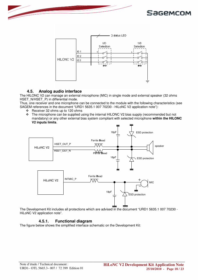
4.5. Analog audio interface
The HILONC V2 can manage an external microphone (MIC) in single mode and external speaker (32 ohms HSET_N/HSET_P) in differential mode. Thus, one receiver and one microphone can be connected to the module with the following characteristics (see SAGEM references in the document “URD1 5635.1 007 70230 - HiLoNC V2 application note”):
� Receiver 32 ohms up to 120 ohms � The microphone can be supplied using the internal HILONC V2 bias supply (recommended but not
mandatory) or any other external bias system compliant with selected microphone within the HILONC V2 inputs limits.
The Development Kit includes all protections which are advised in the document “URD1 5635.1 007 70230 - HiLoNC V2 application note”.
4.5.1. Functional diagram The figure below shows the simplified interface schematic on the Development Kit:
HiLoNC V2
INTMIC_P MIC
Ferrite Bead
18pF ESD protection
HiLoNC V2
HSET_OUT_P
HSET_OUT_N
speaker
Ferrite Bead
Ferrite Bead
18pF
18pF
ESD protection
ESD protection
Note d’étude / Technical document :
URD1– OTL 5665.3– 007 / 72 399 Edition 01 HiLoNC V2 Development Kit Application Note
25/10/2010 - Page 19 / 23
4.6. 51-pins module interface Pad N° Pad name IO Type Description
1 INTMIC_P Analog input Single ended input from microphone
2 AUX_ADC0 Analog input Analog input to digital converter
3 GND Ground GND
4 VGPIO Power supply output +2.8V power supply output
5 VBACKUP Power supply input/output Power supply for RTC backup
6 PWM0 Digital output buffer DC PWM 0
7 RESET Digital input buffer Module Reset
8 SAGEMCOM FACTORY FACTORY purpose
9 SAGEMCOM FACTORY FACTORY purpose
10 SAGEMCOM FACTORY FACTORY purpose
11 TRST Digital bi-directional buffer FACTORY purpose
12 SAGEMCOM FACTORY FACTORY purpose
13 SAGEMCOM FACTORY FACTORY purpose
14 GPIO2 Digital bi-directional buffer General purpose input/output 2
15 GPIO1 Digital bi-directional buffer General purpose input/output 1
16 RF_TX Digital output buffer RF power transmitting indicator
17 PCM_CLK Digital bi-directional buffer PCM clock signal
18 PCM_SYNC Digital bi-directional buffer PCM sync signal
19 PCM_OUT Digital output buffer PCM data output
20 PCM_IN Digital input buffer PCM data input
21 GND Ground GND
22 JTAG1 Digital bi-directional buffer JTAG configuration
23 JTAG2 Digital bi-directional buffer JTAG configuration
24 TEST Digital bi-directional buffer JTAG configuration
25 UART0_RXD Digital input buffer Trace UART0 receive
26 GPIO3 Digital bi-directional buffer General purpose input/output 3
27 GND_RF Ground RF Ground
28 RF Antenna RF signal
29 GND_RF Ground RF Ground
30 VBAT Power supply input +3.7 V power supply (nominal)
31 VBAT Power supply input +3.7 V power supply (nominal)
32 UART0_TXD Digital output buffer Trace UART0 transmit
33 UART1_DSR Digital output buffer UART1 data set ready
34 UART1_DCD Digital output buffer UART1 data carrier detect
35 UART1_RI Digital output buffer UART1 ring indicator
36 UART1_DTR Digital input buffer UART1 data terminal ready
37 UART1_RTS Digital input buffer UART1 request to send
38 UART1_RX Digital input buffer UART1 receive
39 UART1_TX Digital output buffer UART1 transmit
40 UART1_CTS Digital output buffer UART1 clear to send
41 POK_IN Digital input Module power on signal
Note d’étude / Technical document :
URD1– OTL 5665.3– 007 / 72 399 Edition 01 HiLoNC V2 Development Kit Application Note
25/10/2010 - Page 20 / 23
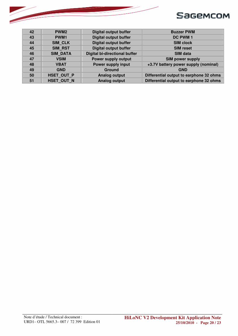
42 PWM2 Digital output buffer Buzzer PWM
43 PWM1 Digital output buffer DC PWM 1
44 SIM_CLK Digital output buffer SIM clock
45 SIM_RST Digital output buffer SIM reset
46 SIM_DATA Digital bi-directional buffer SIM data
47 VSIM Power supply output SIM power supply
48 VBAT Power supply input +3.7V battery power supply (nominal)
49 GND Ground GND
50 HSET_OUT_P Analog output Differential output to earphone 32 ohms
51 HSET_OUT_N Analog output Differential output to earphone 32 ohms
Note d’étude / Technical document :
URD1– OTL 5665.3– 007 / 72 399 Edition 01 HiLoNC V2 Development Kit Application Note
25/10/2010 - Page 21 / 23
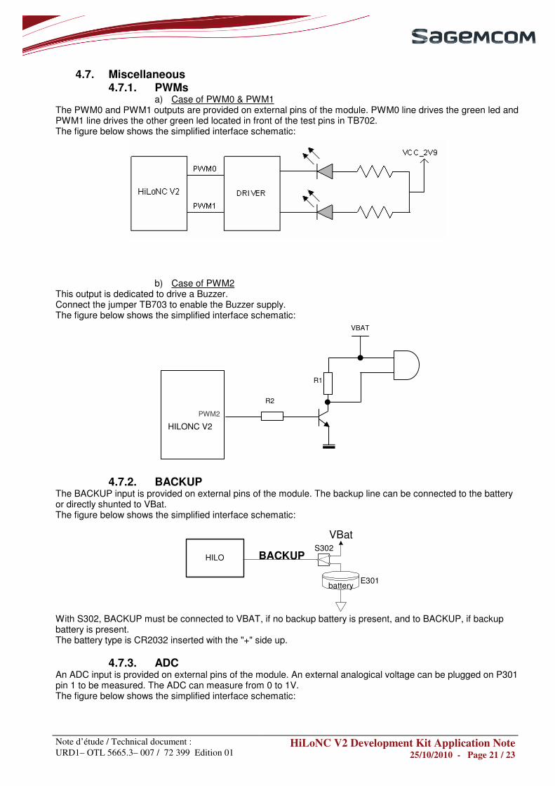
4.7. Miscellaneous 4.7.1. PWMs
a) Case of PWM0 & PWM1 The PWM0 and PWM1 outputs are provided on external pins of the module. PWM0 line drives the green led and PWM1 line drives the other green led located in front of the test pins in TB702. The figure below shows the simplified interface schematic:
b) Case of PWM2
This output is dedicated to drive a Buzzer. Connect the jumper TB703 to enable the Buzzer supply. The figure below shows the simplified interface schematic:
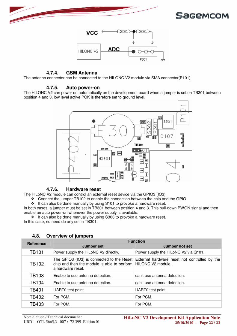
4.7.2. BACKUP The BACKUP input is provided on external pins of the module. The backup line can be connected to the battery or directly shunted to VBat. The figure below shows the simplified interface schematic:
HILO
battery
VBat
BACKUPS302
E301
With S302, BACKUP must be connected to VBAT, if no backup battery is present, and to BACKUP, if backup battery is present. The battery type is CR2032 inserted with the "+" side up.
4.7.3. ADC An ADC input is provided on external pins of the module. An external analogical voltage can be plugged on P301 pin 1 to be measured. The ADC can measure from 0 to 1V. The figure below shows the simplified interface schematic:
R1
R2
HILONC V2
VBAT
PWM2
Note d’étude / Technical document :
URD1– OTL 5665.3– 007 / 72 399 Edition 01 HiLoNC V2 Development Kit Application Note
25/10/2010 - Page 22 / 23
4.7.4. GSM Antenna The antenna connector can be connected to the HILONC V2 module via SMA connector(P101).
4.7.5. Auto power-on The HILONC V2 can power on automatically on the development board when a jumper is set on TB301 between position 4 and 3, low level active POK is therefore set to ground level.
4.7.6. Hardware reset The HiLoNC V2 module can control an external reset device via the GPIO3 (IO3).
� Connect the jumper TB102 to enable the connection between the chip and the GPIO. � It can also be done manually by using S101 to provoke a hardware reset.
In both cases, a jumper must be set in TB301 between position 4 and 3. This pull-down PWON signal and then enable an auto power-on whenever the power supply is available.
� It can also be done manually by using S303 to provoke a hardware reset. In this case, no need do any set in TB301.
4.8. Overview of jumpers Function
Reference Jumper set Jumper not set
TB101 Power supply the HiLoNC V2 directly. Power supply the HiLoNC V2 via Q101.
TB102 The GPIO3 (IO3) is connected to the Reset chip and then the module is able to perform a hardware reset.
External hardware reset not controlled by the HILONC V2 module.
TB103 Enable to use antenna detection. can’t use antenna detection.
TB104 Enable to use antenna detection. can’t use antenna detection.
TB401 UART0 test point. UART0 test point.
TB402 For PCM. For PCM.
TB403 For PCM. For PCM.
Note d’étude / Technical document :
URD1– OTL 5665.3– 007 / 72 399 Edition 01 HiLoNC V2 Development Kit Application Note
25/10/2010 - Page 23 / 23
TB404 For PCM. For PCM.
TB405 For PCM. For PCM.
TB703 Buzzer Enabled Buzzer Disabled
TB704 The pin SIM card presence detection from the SIM card holder pins 9 & 10 is connected to the GPIO2 (IO2).
The pin SIM card presence detection from the SIM card holder pins 9 & 10 is not connected to the GPIO2 (IO2).
4.9. Overview of Switchers
Function Reference
Switch on Switch off
S701 To set up GPIO1 to GPIO3 as an input. To set up GPIO1 to GPIO3 as an output.
S702 Pulls down GPIO1 to GPIO3 when they are set up as input.
Pulls up GPIO1 to GPIO3 when they are set up as input.
S301 POWER ON the HILONC V2 module. No action.
S101 Shut down the power supply. No action.
S303 Provoke a hardware reset. No action.
Function
Reference Position 1 Position 2
S302 Connects BACKUP signal of module to the backup battery. (CR2032: lithium battery of 3V)
Connects BACKUP signal of module to the VBAT.
S601 SIM CARD is selected. SIM IC is selected.
S304 Reserved by Sagemcom. Reserved by Sagemcom.
S305 Reserved by Sagemcom. Reserved by Sagemcom.
S306 Reserved by Sagemcom. Reserved by Sagemcom.
~END OF DOCUMENT ~

All
righ
ts r
ese
rve
d.
Th
e in
form
atio
n a
nd
specific
ations inclu
de
d a
re s
ubje
ct to
chan
ge w
ith
out
pri
or
notice. S
ag
em
co
m t
ries t
o e
nsure
that
all
info
rma
tio
n in t
his
docum
en
t is
corr
ect,
but
doe
s n
ot
accept lia
bili
ty fo
r e
rror
or
om
issio
n.
No
n c
ontr
actu
al docu
men
t..
All
tra
de
mark
s a
re r
egis
tere
d b
y t
heir
resp
ective
ow
ne
rs.


![MANUEL DU PILOTE D'IMPRIMANTE XPS - Support …support.sagemcom.com/site/livret/090318_XPS_fr.pdf · propriétés du pilote d'imprimante. † Option [Sélection automatique] sélectionnée](https://static.fdocuments.net/doc/165x107/5b9b3b2509d3f292798cb76a/manuel-du-pilote-dimprimante-xps-support-proprietes-du-pilote-dimprimante.jpg)