Highly porous ZnO thin films and 1D nanostructures by...
27
- 1 - ((please add journal code and manuscript number, e.g., DOI: 10.1002/ppap.201100001)) Article type: Full Paper Highly porous ZnO thin films and 1D nanostructures by remote plasma processing of Zn-phthalocyanine a Maria Alcaire, A. Nicolas Filippin, Manuel Macias-Montero, Juan R. Sanchez-Valencia, T. Cristina Rojas, Ana Mora-Boza, Carmen Lopez-Santos, Juan P. Espinos, Angel Barranco and Ana Borras* ––––––––– Materials Science Institute of Seville (ICMSE, CSIC-US), Avd. Americo Vespucio 49, 41092, Seville, Spain ––––––––– In this paper the fabrication of highly porous ZnO layers and 1D nanostructures by a vacuum and plasma etching combined protocol is presented. Zn-phthalocyanine (ZnPc) is utilized as a solid precursor to form the ZnO. First the ZnPc is sublimated in low argon pressure. Depending on the substrate temperature and microstructure, polycrystalline films or single crystal ZnPc nanowires are grown. These starting materials are then subjected to a remote plasma oxidizing treatment. Experimental parameters such as substrate position, plasma power, treatment duration and substrate temperature determine the microstructure and properties of the final ZnO nanostructures. The article gathers an in depth study of the obtained porous nanostructured films following scanning and transmission electron microscopy (SEM and TEM), X-ray photoelectron spectroscopy (XPS), X-ray Diffraction (XRD), UV-Vis transmittance and fluorescence spectroscopies. Introduction ZnO is a direct wide band-gap semiconductor (~3.37 eV) with a large exciton binding energy of ~60 meV with interesting applications in photocatalysis, optics, piezoelectricity and wetting. 1,2 Lately, much attention has been focused on the investigation of the fabrication methods and the specific properties of ZnO 1D nanostructures. 1,3-11 In fact, many applications have been developed for both single ZnO 1D nanostructures or films formed by a high density of them in fields such as nanosensors, solar cells and photovoltaics, photonic devices, a Supporting Information is available at Wiley Online Library or from the author.
Transcript of Highly porous ZnO thin films and 1D nanostructures by...

- 1 -
((please add journal code and manuscript number, e.g., DOI: 10.1002/ppap.201100001))
Article type: Full Paper
Highly porous ZnO thin films and 1D nanostructures by remote plasma
processing of Zn-phthalocyaninea
Maria Alcaire, A. Nicolas Filippin, Manuel Macias-Montero, Juan R. Sanchez-Valencia, T.
Cristina Rojas, Ana Mora-Boza, Carmen Lopez-Santos, Juan P. Espinos, Angel Barranco and
Ana Borras*
–––––––––
Materials Science Institute of Seville (ICMSE, CSIC-US), Avd. Americo Vespucio 49,
41092, Seville, Spain
–––––––––
In this paper the fabrication of highly porous ZnO layers and 1D nanostructures by a vacuum
and plasma etching combined protocol is presented. Zn-phthalocyanine (ZnPc) is utilized as a
solid precursor to form the ZnO. First the ZnPc is sublimated in low argon pressure.
Depending on the substrate temperature and microstructure, polycrystalline films or single
crystal ZnPc nanowires are grown. These starting materials are then subjected to a remote
plasma oxidizing treatment. Experimental parameters such as substrate position, plasma
power, treatment duration and substrate temperature determine the microstructure and
properties of the final ZnO nanostructures. The article gathers an in depth study of the
obtained porous nanostructured films following scanning and transmission electron
microscopy (SEM and TEM), X-ray photoelectron spectroscopy (XPS), X-ray Diffraction
(XRD), UV-Vis transmittance and fluorescence spectroscopies.
Introduction
ZnO is a direct wide band-gap semiconductor (~3.37 eV) with a large exciton binding
energy of ~60 meV with interesting applications in photocatalysis, optics, piezoelectricity and
wetting.1,2
Lately, much attention has been focused on the investigation of the fabrication
methods and the specific properties of ZnO 1D nanostructures.1,3-11
In fact, many applications
have been developed for both single ZnO 1D nanostructures or films formed by a high density
of them in fields such as nanosensors, solar cells and photovoltaics, photonic devices,
a Supporting Information is available at Wiley Online Library or from the author.

- 2 -
photocatalysis and, very recently, as an active component in microfluidics.7-13
An ample
variety of methods for the fabrication of nanostructured ZnO have been reported. One of the
most popular is the hydrothermal growth of single crystal ZnO nanowires from several
precursors such as zinc nitrate hydrate in the initial presence of ZnO in the form of quantum
dots14
or thin film,15
with a seed layer prepared from a zinc acetate solution.16,17
Several
vacuum deposition methodologies have been applied as well, for instance, vapor transport and
condensation (CVTC) processes for the synthesis of ZnO nanowires via a vapor-liquid-solid
(VLS) mechanism from ZnO powders at high temperatures (800-1000 ºC) in the presence of
Au seeds.18-22
Plasma routes have also successfully worked for the development of porous
ZnO thin films, ZnO 1D nanostructures and heterostructures.23-26
In our laboratory, we have
recently focused our attention on the development of the plasma enhanced chemical vapor
deposition (PECVD) processes at mild temperatures of diethyl zinc as a precursor for the
growth of tunable luminescent thin films27
and heterostructured Ag-ZnO nanorods.28
Reference 29 gathers the most interesting results on the plasma growth of ZnO thin films for
optical sensing of oxygen. The hydrothermal and CVTC methods provide nanowires with the
wurtzite structure that present a compact microstructure, which is greatly responsible for their
attractive transport properties. Chemical vapor deposition (CVD), metalorganic chemical
vapor deposition (MOCVD) and conventional magnetron approaches yield compact thin
films, usually utilized as high refractive index layers and blocking layers in different devices
such as dye sensitized solar cells.9 PECVD thin films are characterized by a columnar
microstructure involving micro and mesopores. Plasma gas composition and substrate
temperature control the texture of these nanocrystalline films. To the best of our knowledge,
the lowest refractive index published so far for a ZnO thin film is between 1.8 and 1.9.30-32
In
this work, we will study an alternative plasma route for the formation of ZnO layers and
nanowires. The main objective of the work is to extrapolate the plasma etching method
previously developed in reference 28 for the fabrication of metal decorated and hierarchical

- 3 -
organic nanowires (ONWs), to the formation of metal oxide layers and 1D nanostructures.33
Concretely, we will demonstrate the advantageous use of ZnPc as precursor for highly porous
ZnO materials. The effect of different experimental parameters (i.e. plasma power, holder
position, substrate temperature, thickness of the precursor materials and treatment duration)
on the microstructure, optical properties and composition of the final nanostructures will be
evaluated. The paper gathers an in depth characterization of the microstructure (SEM, TEM
and high angle annular dark field scanning transmission electron microscopy (HAADF-
STEM), structure (XRD), composition (XPS) and optical properties (UV-Vis and
fluorescence) of the different porous nanostructures obtained.
Experimental Section
Scheme S1 summarizes the different steps for the formation of the ZnO layers (Scheme S1
a) and highly porous nanowires (Scheme S1 b). The two main steps involved in the procedure
are i) the formation of the ZnPc starting materials, either in the form of a thin film or as a high
density of supported ONW by physical vapor deposition (PVD) and the subsequent ii) in situ
etching by oxygen plasma. In the case of the nanowires an additional step is required (i-0) to
fabricate the metal nanoparticles layers or oxide thin films acting as nucleation centers for the
growth of the ONWs.30
The position of the precursor sample with respect to the plasma glow
discharge will be referred from now on as “front-face” for the samples treated facing up to the
plasma, and “down-face” for samples treated beneath the holder. The following paragraphs
describe the experimental details in this work.
Deposition of ZnPc thin films and ONWs: Zinc phthalocyanine (ZnPc) (Sigma-Aldrich)
was used as received. Previous to the deposition, the system was pumped down to a base
pressure of 10-6
mbar. The sublimation of the molecule was carried out using a Knudsen cell,
placed at 8 cm from the substrates, under 10-2
mbar of Ar, which was regulated by a calibrated
mass flow controller. Growth rate and equivalent thickness of the ZnPc were monitored using
a quartz crystal microbalance (QCM), and the growth rate adjusted to 0.3 Å/s. In the course of

- 4 -
this paper we will distinguish between the nominal or equivalent thickness, i.e. acquired with
the QCM, and the actual thickness measure by SEM or optical methods. For the thin films, the
nominal thickness was varied in the range between 100 and 450 nm, while for the nanowires
was chosen at around 200 nm. Table S1 summarizes the nominal and SEM thicknesses of the
different samples deposited as precursor layers. The substrate temperature was about 30 ºC in
the case of the thin films deposition and 175 ºC to induce the formation of the organic
nanowires. Heating of the substrate holder up to 175 ºC was provided by a homemade hot
plate consisting of a nichrome filament connected to the sample holder through a ceramic
envelope. Substrate temperature during the evaporation step was measured by a thermocouple
in contact with the sample holder.
Prior to the synthesis of the ZnPc NWs, sputtered gold nanoparticles were used to create
seeds for the growing process. Gold NPs were fabricated by using a commercially available
K550 sputter source from Emitech. This source is calibrated to produce a gold deposition rate
proportional to the deposition current. The apparatus operates at low voltage in the range 100-
150 Volts as indicated by the manufacturer. The working conditions for the gold sputtering
process were 12.5 mA for the current intensity and 15 seconds of duration.
Soft etching by ECR-MW oxygen plasma: Different oxygen etching treatments were
carried out on the sublimated ZnPc thin films and nanowires in a microwave electron
cyclotron resonance (MW-ECR) set up detailed elsewhere.27-29
Table 1 gathers the
experimental conditions chosen for the oxygen plasma etching of the sublimated samples.
Samples labelling addresses main experimental parameters during the etching treatment,
indicating position of the sample (down- (D) or front (F) –facing to the plasma discharge),
power applied to the plasma, substrate temperature and treatment duration. During all these
treatments the chamber pressure was set to 10-3
mbar of oxygen and the distance between the
substrates and the glow discharge region was fixed at 4 cm.

- 5 -
Table 1. Experimental conditions chosen for the oxygen plasma etching treatments at 10-3
mbar. Treatments from T1 to T9 were carried out on thin films while T’1 to T’3 refers to
treatment on supported ONWs.
Sample Label Position Power
[W]
Temperature
[ºC]
Runtime [hours]
T1 (D-150W-RT-2h) DOWN 150 RT 2
T2 (D-150W-150ºC-2h) DOWN 150 150 2
T3 (F-150W-150ºC-2h) FRONT 150 150 2
T4 (D-270W-RT-4h) DOWN 270 RT 4
T5 (D-270W-150ºC-4h) DOWN 270 150 4
T6 (D-270W-200ºC-2h) DOWN 270 200 2
T7 (F-270W-RT-4h) FRONT 270 RT 4
T8 (F-270W-150ºC-4h) FRONT 270 150 4
T9 (F-270W-200ºC-2h) FRONT 270 200 2
T´1 (D-270W-RT-1h) DOWN 270 RT 1
T´2 (D-270W-RT-2h) DOWN 270 RT 2
T´3 (D-270W-RT-4h) DOWN 270 RT 4
Experimental characterization methods: High-resolution SEM images of the samples
deposited on silicon wafers were obtained in a Hitachi S4800 microscope, working at
different acceleration voltages (1-5 kV). Cross sectional views were obtained by cleaving the
Si(100) substrates. Bright field TEM images were obtained in a CM200 apparatus from
Philips. HAADF-STEM images were acquired in a Tecnai G2F30 S-Twin STEM from FEI.
The mean diameter of the ZnO nanoparticles and coverage area of the thin films have been
calculated through the analysis of HAADF-STEM and SEM images correspondently with the
free software ImageJ. XPS experiments were performed in a Phoibos 100 DLD X-ray
spectrometer from SPECS. The spectra were collected in the pass energy constant mode at a
value of 50 eV using a Mg Kα source. C1s signal at 284.5 eV was utilized for calibration of
the binding energy in the spectra. The assignment of the BE to the different elements in the
spectra corresponds to the data in reference 34. Glancing Angle X-ray Diffraction was carried
out in a Panalytical X'PERT PRO diffractometer at glancing angle of 0.2 º. UV-Vis
transmission spectra of samples deposited on fused silica slides were recorded in a Cary 100
spectrophotometer in the range from 190 to 900 nm. Fluorescence spectra were recorded in a

- 6 -
Jobin Yvon Fluorolog3 spectrofluorometer using the front face configuration and grids of 5
and 8 nm for the excitation and emission monochromators, respectively.
Results and Discussion
Organic thin films and single crystal nanowires by Physical Vapor Deposition of ZnPc
Figure 1 presents representative cross section and normal view images of two ZnPc thin
films with a measured thickness of 200 nm (Fig. 1 a-b) and 775 nm (Fig. 1 c-d) respectively.
The thicker ZnPc thin film shows a columnar feather-like microstructure, with a broad
distribution of diameters (50-100 nm) measured at the mean height of the columns and an
average length of 500 nm. It is clearly visible in the image that the column formation is
preceded by a granular region at the interface with the substrate of about 90 nm. The
dependence of the microstructure with the sample thickness is confirmed in panel a) of the
same figure for the cross section of a thinner film. The image reveals quite inhomogeneous
features forming a granular layer, where only incipient columns are visible. Although Fig. 1 a)
shows at first glance that these grains are agglomerated; normal view image (Fig. 1 b)
presents separate particles, in agreement with the very first stages of columnar growth. We
did not observe a constant relationship between the nominal thickness (monitored by a QCM)
and the actual thickness measured by SEM (see Table S1). This apparent disagreement is in
part due to differences in the growth rates corresponding to the granular and columnar
regimes.
- 7 -
ZnPc thin film (200nm)
500 nm500 nm
a) b)
ZnPc nanowires on Au NPs
500 nm
ZnPc thin film (775nm)
500 nm
c) d)
1 um1 um
e) f)
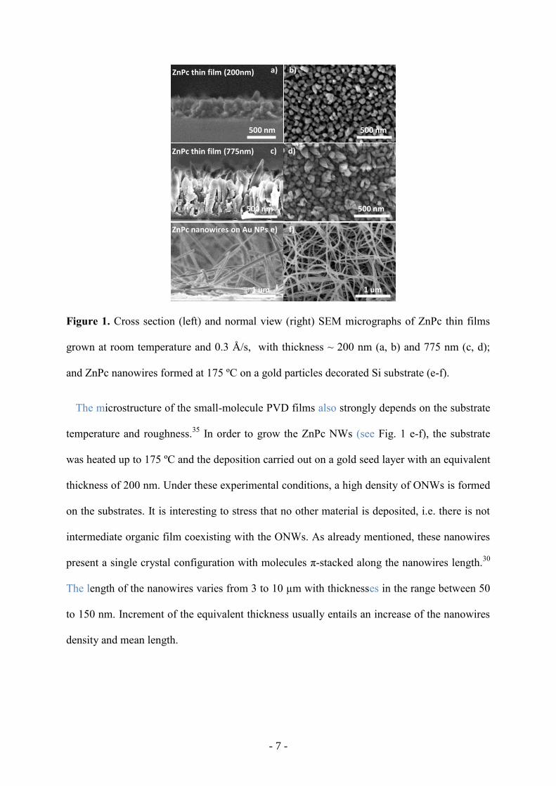
Figure 1. Cross section (left) and normal view (right) SEM micrographs of ZnPc thin films
grown at room temperature and 0.3 Å/s, with thickness ~ 200 nm (a, b) and 775 nm (c, d);
and ZnPc nanowires formed at 175 ºC on a gold particles decorated Si substrate (e-f).
The microstructure of the small-molecule PVD films also strongly depends on the substrate
temperature and roughness.35
In order to grow the ZnPc NWs (see Fig. 1 e-f), the substrate
was heated up to 175 ºC and the deposition carried out on a gold seed layer with an equivalent
thickness of 200 nm. Under these experimental conditions, a high density of ONWs is formed
on the substrates. It is interesting to stress that no other material is deposited, i.e. there is not
intermediate organic film coexisting with the ONWs. As already mentioned, these nanowires
present a single crystal configuration with molecules π-stacked along the nanowires length.30
The length of the nanowires varies from 3 to 10 µm with thicknesses in the range between 50
to 150 nm. Increment of the equivalent thickness usually entails an increase of the nanowires
density and mean length.
- 8 -
Oxygen plasma etching of ZnPc thin films
Thin films and ONWs presented in the previous section were used as starting materials for
the formation of ZnO by soft plasma etching in a down-stream configuration. The idea behind
this approach being the fabrication of ZnO using the Zn atom in the ZnPc molecule by the
application of an oxygen plasma with the aim to form highly porous metal oxide layers.
Microstructure, porosity and chemical composition.
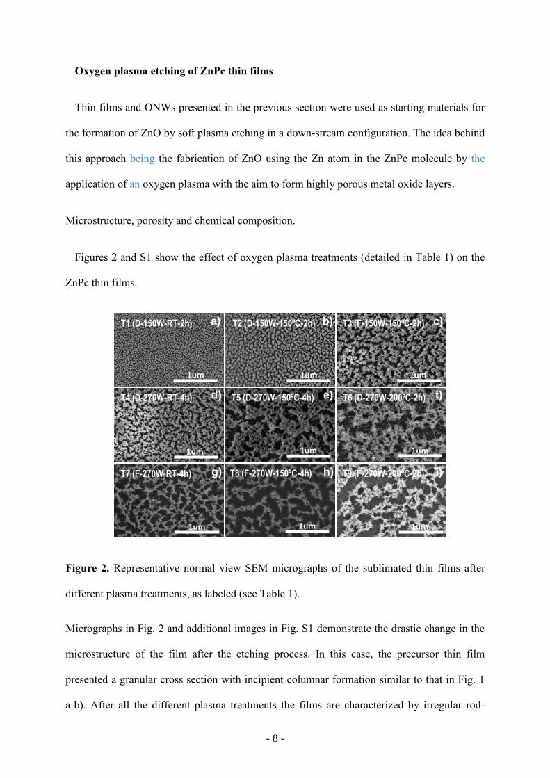
Figures 2 and S1 show the effect of oxygen plasma treatments (detailed in Table 1) on the
ZnPc thin films.
1um
1um
1um
T1 (D-150W-RT-2h)
1um 1um
S+T5
1um
1um
1um
1um
a) c)T2 (D-150W-150ºC-2h) T3 (F-150W-150ºC-2h)
T4 (D-270W-RT-4h) T5 (D-270W-150ºC-4h)
T7 (F-270W-RT-4h) T8 (F-270W-150ºC-4h) T9 (F-270W-200ºC-2h)
T6 (D-270W-200ºC-2h)
b)
d) f)e)
g) i)h)
Figure 2. Representative normal view SEM micrographs of the sublimated thin films after
different plasma treatments, as labeled (see Table 1).
Micrographs in Fig. 2 and additional images in Fig. S1 demonstrate the drastic change in the
microstructure of the film after the etching process. In this case, the precursor thin film
presented a granular cross section with incipient columnar formation similar to that in Fig. 1
a-b). After all the different plasma treatments the films are characterized by irregular rod-

- 9 -
bundles in the cross section and a foam-like top view with interconnected macropores, i.e.
porous with diameters in the range of hundreds of nanometers. Table 2 summarizes the effect
of the plasma treatments on sample thicknesses and coverage area, this latter calculated
through the image analysis of normal view of the surface in Fig. 2. Comparison between Fig.
2 a) and b) indicates that the increment in substrate temperature from RT to 150 ºC increases
the size of the bundles and the open area between them. Exposing the samples directly to the
plasma discharge also produces an increment of the macroporosity, i.e. a reduction of the
coverage. This is clear by comparing Fig. 2 d) and g), e) and h) and f) and i) where for the
same sample thickness, substrate temperature, plasma power and run time, the samples treated
face to the plasma present a much more pronounced open porosity. In general an increase of
the run time leads to a similar result, although the effect of the substrate temperature is more
critical. For instance, a slight difference temperature of 50 ºC drastically reduces the time to
achieve the desired open porosity and oxidation of the ZnPc as we will demonstrate in the
next section. For the run time effect see the comparison between Fig. 2 e) and f) or h) and i),
where 2 hours at 200 ºC treatment (f and i) produces a similar effect than 4 hours at 150 ºC (e
and h). As expected for the nature of the methodology, the plasma etching treatments reduce
the thickness of the sample (Table 2). At higher temperatures this reduction is more
pronounced, see for instance effects of T1 (RT) and T2 (150ºC) on the same initial thickness
leading to a reduction in thickness of the 30% in the first case in comparison to the 55 % at
high temperature. In the same way, treatments with samples facing up the plasma discharge
present a higher efficiency than down-face experiments (compare T6 and T9 in Table 2). A
similar result is obtained by increment of the treatment duration. Thus, for instance, T5
carried out during 4 hours produces a thickness reduction ~ 31 % while T6 yielded at higher
temperatures but 2 hours provokes a reduction in thickness of only a ~ 21 %. These
reproducible and accordingly results in samples thicknesses are not directly extendable to the
surface coverage. In fact, there is not a straightforward relationship between the thickness of

- 10 -
the sample or experimental etching parameters and the final porosity as addressed by last
column in Table 2. It is worth stressing that we aim here only to a semi-quantitative
evaluation of the plasma effects since the highly roughness of the samples (see Fig. S1 a)
hampers an accurate measurement of the sample thickness, being the error bars corresponding
to the first column in Table 2 in the order of nanometers while these bars might be in the order
of tens of nanometers in the second column.
Table 2. Effect of the post-treatment on the sample thickness and coverage area.
Sample Initial thickness
(SEM) (nm)
Pos-treatment
Thickness
(SEM) (nm)
Thickness
reduction (%) Coverage
(%)
T1 (D-150W-RT-2h) 200 140 30 73
T2 (D-150W-150ºC-2h) 200 90 55 73
T3 (F-150W-150ºC-2h) 775 450 28 68
T4 (D-270W-RT-4h) 650 356 54 64
T5 (D-270W-150ºC-4h) 400 277 31 60
T6 (D-270W-200ºC-2h) 400 317 21 61
T7 (F-270W-RT-4h) 650 153 76 61
T8 (F-270W-150ºC-4h) 400 210 47.5 55
T9 (F-270W-200ºC-2h) 400 274 31.5 55
Figure 3 shows the GA-XRD diagrams acquired for a set of selected samples. The X-ray
diffractogram of the sublimated ZnPc thin film is dominated by a peak at 2θ = 6.9° that
corresponds to an interplanar spacing, d, of 12.8 Å, and are due to the diffraction from the
(200) plane of the α-form of ZnPc. The intensity of this peak depends on the sample
thickness.36
Conversion of ZnPc into ZnO, i.e. degradation of the organic polycrystalline
layer, must be accompanied by the amorphization of the sublimated film. Results in Fig. 3
demonstrates that the plasma etching treatments carried out in a down face configuration
require high temperature conditions (200 ºC, T6) to complete the amorphization of the
sample. The front-face condition is effective even for oxidation at room temperature of thick
samples (T7). It is important to point out herein that the amorphization of the ZnPc is not
compensated by the apparent formation of crystalline ZnO (see reference 25). In fact, the ZnO
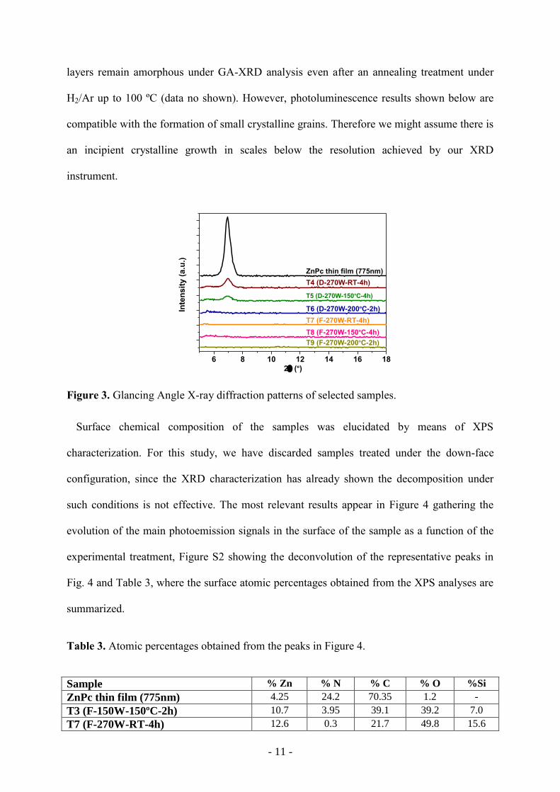
- 11 -
layers remain amorphous under GA-XRD analysis even after an annealing treatment under
H2/Ar up to 100 ºC (data no shown). However, photoluminescence results shown below are
compatible with the formation of small crystalline grains. Therefore we might assume there is
an incipient crystalline growth in scales below the resolution achieved by our XRD
instrument.
6 8 10 12 14 16 18
Inte
ns
ity
(a
.u.)
2 (º)
ZnPc thin film (775nm)
T4 (D-270W-RT-4h)
T5 (D-270W-150ºC-4h)
T6 (D-270W-200ºC-2h)
T7 (F-270W-RT-4h)
T8 (F-270W-150ºC-4h)
T9 (F-270W-200ºC-2h)
Figure 3. Glancing Angle X-ray diffraction patterns of selected samples.
Surface chemical composition of the samples was elucidated by means of XPS
characterization. For this study, we have discarded samples treated under the down-face
configuration, since the XRD characterization has already shown the decomposition under
such conditions is not effective. The most relevant results appear in Figure 4 gathering the
evolution of the main photoemission signals in the surface of the sample as a function of the
experimental treatment, Figure S2 showing the deconvolution of the representative peaks in
Fig. 4 and Table 3, where the surface atomic percentages obtained from the XPS analyses are
summarized.
Table 3. Atomic percentages obtained from the peaks in Figure 4.
Sample % Zn % N % C % O %Si
ZnPc thin film (775nm) 4.25 24.2 70.35 1.2 -
T3 (F-150W-150ºC-2h) 10.7 3.95 39.1 39.2 7.0
T7 (F-270W-RT-4h) 12.6 0.3 21.7 49.8 15.6

- 12 -
T9 (F-270W-200ºC-2h) 24.2 0.3 20.9 48.1 6.5
As shown in Fig. 4 a-b), the intensities of the Zn2p and ZnL3M45M45 peaks drastically rise,
as expected for the mineralization of the phtalocyanine. Moreover, the constancy of the shape
and energy position of the Zn2p and ZnL3M45M45 signals demonstrates that zinc species are
always divalent. It is expected that the complete conversion of ZnPc into ZnO to be
accompanied by the diminishing of the surface concentration of nitrogen (Fig. 4 d) and carbon
(Fig. 4 c) and the appearance of oxygen (Fig. 4 d) (see also Table 3) whose binding energy
agree with those ones expected for oxide (529-530 eV), hydroxide (~531 eV) and
carbonate/carboxilate (531.5-532 eV) species. A first glance of results in Table 3 and Figs. 4
d) and Fig. S2 e)-h) shows that the practical disappearance of nitrogen, i.e. decomposition of
the phthalocyanine, only occurs for samples T7 (F-270W-RT-4h) and T9 (F-270W-200ºC-2h)
with treatments carried out applying a plasma power of 270 W. Sample subjected to plasma at
150 W (T3 (F-150W-150ºC-2h)) has been only partially converted to ZnO. In addition, the
percentage of carbon decreases drastically for all the cases analyzed (Fig. 4 c) and Fig. S2 i).

- 13 -
150 100 50 0
S2p
VB
Si, SiOx
Zn3s
Inte
ns
ity
(a
.u.)
BE (eV)
Zn3p
SiO2SiO
2Si, SiO
x
Si2sSi2p
295 290 285 280 275
T9
T7
T3
ZnPc thin film
Inte
ns
ity
(a
.u.)
BE (eV)
1025 1020 1015
T9
T7
T3
ZnPc thin film
Inte
ns
ity
(a
.u.)
BE (eV)
405 400 395 390
T9
T7
T3
ZnPc thin film
Inte
ns
ity
(a
.u.)
BE (eV)
540 535 530 525
T9
T7
T3
ZnPc thin film
Inte
ns
ity
(a
.u.)
BE (eV)
505 500 495 490
T9
T7
T3
ZnPc thin film
Inte
ns
ity
(a
.u.)
BE (eV)
a) Zn 2p b) ZnL3M45M45
c) C1s d) N1s
e) O1s f)
Figure 4. Representative XPS spectra of selected samples as labeled: ZnPc thin film (775nm),
T3 (F-150W-150ºC-2h), T7 (F-270W-RT-4h) and T9 (F-270W-200ºC-2h).
It is also interesting to follow the evolution of the silicon peaks coming from the exposed
substrate (Fig. 4 f). For the sublimated sample there is no trace of silicon, meaning that the
original columnar nanostructure covers the substrate completely. However, silicon is exposed
for all the treatments in Table 3, being the most effective treatment T7 (F-270W-RT-4h). This
is in good agreement with the open porosity claimed in the previous section. Moreover, part
of the silicon turns into silica after the plasma treatment. Sample T7 (F-270W-RT-4h) is the
only showing a complete oxidation of the substrate. These results indicate that the runtime of
the treatment (240 min for sample T7 while 120 min for the other two) plays a critical role.
Thus, increasing the runtime of the operation allows the decomposition at room temperature
even for thick samples. It is also worthy to note that the enrichment in the oxygen atomic
concentration presented in Table 3 is in part related with the exposing of uncovered areas of
the oxidized silicon substrate. This amount of oxygen along with the corresponding to the

- 14 -
formation of carbonate/carboxilate species are responsible for the apparent discording
between Zn and O atomic concentration that in a stoichiometric sample should appear 1:1.
Optical properties
Figure 5 a-b) shows the UV-Vis transmittance spectra of the different samples fabricated on
fused silica. The sublimated Zn-phthalocyanine (black line in Fig. 5) shows the typical
transmission spectrum with two strong absorptions, the first one in the UV region at about
300 – 400 nm (B band) and a second one in the visible part of the spectrum around 600 – 700
nm (Q band). B band arises from the deeper π-levels → LUMO transition while the Q band is
attributed to the π – π* transition from the highest occupied molecular orbital (HOMO) to the
lowest unoccupied molecular orbital (LUMO) of the of the pi resonant system of the
porphyrinic ring ring.37
The transmittance spectra corresponding to samples T1 to T4 are
dominated by the remaining phthalocyanine after plasma treatment, in good agreement with
the results discussed in the previous section. It is therefore required treatments of the samples
exposed to the plasma, high temperature of the substrates and/or prolonged times in order to
reduce the B and Q bands (treatments T6 to T9). It must be noted that the total vanishing of
the ZnPc bands does not proceed with the rise of new absorption bands in the visible range,
while a strong band around 350 nm should be expected if ZnO is formed due to the band gap
of the semiconductor. However, curves in Fig. 5 a, b) do not show such a strong absorption
below this wavelength. The reason for the high transparency of the samples below the band
gap of ZnO could relay in the low coverage of the substrate, as a great deal of light is
transmitted straightforward through the fused silica substrate. A more appealing feature is
shown in the zoom-in in Fig. 5 b), the lines corresponding to treatments T7 (F-270W-RT-4h),
T8 (F-270W-150ºC-4h) and T9 (F-270W-200ºC-2h) do not show the typical oscillations
arising from the partial reflection of the light in the interface with the substrate, and the
optical transmission is even higher than the corresponding to the uncoated fused silica

- 15 -
substrate. These results might indicate an antireflective behavior of the plasma treated films.
In order to estimate the refractive index, we have fitted the spectra for sample T7 (F-270W-
RT-4h) (See also SI Section S1 and Figures S3-S5 for further information). The value for the
calculated refractive index by this fitting is extremely low: n (550nm) = 1.11 for an adjusted
optical thickness of t = 135 nm. The slight difference in thickness, in comparison with the one
in Table 2 (153 nm), is easily justified by the high roughness and inhomogeneity of the cross
section of the sample. Application of effective medium approximations to the estimation of
the refractive index yields porosity values above 90 % for the selected sample (Fig. S4).
200 400 600 800
86
88
90
92
94
96
Tra
ns
mit
tan
ce
(%
)
Wavelength (nm)
Fused silica
100 200 300 400 500 600 700 800 900 1000
0
20
40
60
80
100
ZnPc (400nm)
T1(D-150W-RT-2h)
T2(D-150W-150ºC-2h)
T3(F-150W-150ºC-2h)
T4(D-270W-RT-4h)
T6(D-270W-200ºC-2h)
T7(F-270W-RT-4h)
T8(F-270W-150ºC-4h)
T9(F-270W-200ºC-2h)
Tra
ns
mit
tan
ce
(%
)
Wavelength (nm)
Fused silica
Figure 5. a) Transmittance spectra of the sublimated thin film ZnPc (400nm) and plasma
treated samples, b) Zoom-in showing the transmittance above the fused silica spectrum for the
total oxidized films.
Due to its wide band gap (~3.37 eV at room temperature) and high exciton energy (60 meV),
ZnO presents an ultraviolet luminescence band (E-band) related to excitonic radiative

- 16 -
recombinations that is of prime interest for the realization of electroluminescent diodes or
room temperature UV lasers. In addition, ZnO might present other luminescence bands in the
visible range (D-band). The presence of D-bands has been ascribed to defect related energy
levels between the conduction and valence bands. Depending on the fabrication conditions,
native defects (such as oxygen or Zn vacancies and interstitials and oxygen anti-sites) or
extrinsic defects (such as nitrogen or metal heteroatoms) can be introduced into the network
and thus lead to the control of the electronic structure of the material and consequently to the
tailoring of its luminescence response in the visible range. Defects can be located in the
volume or at the surface of the material in a proportion that is likely to be controlled by the
synthesis process.27
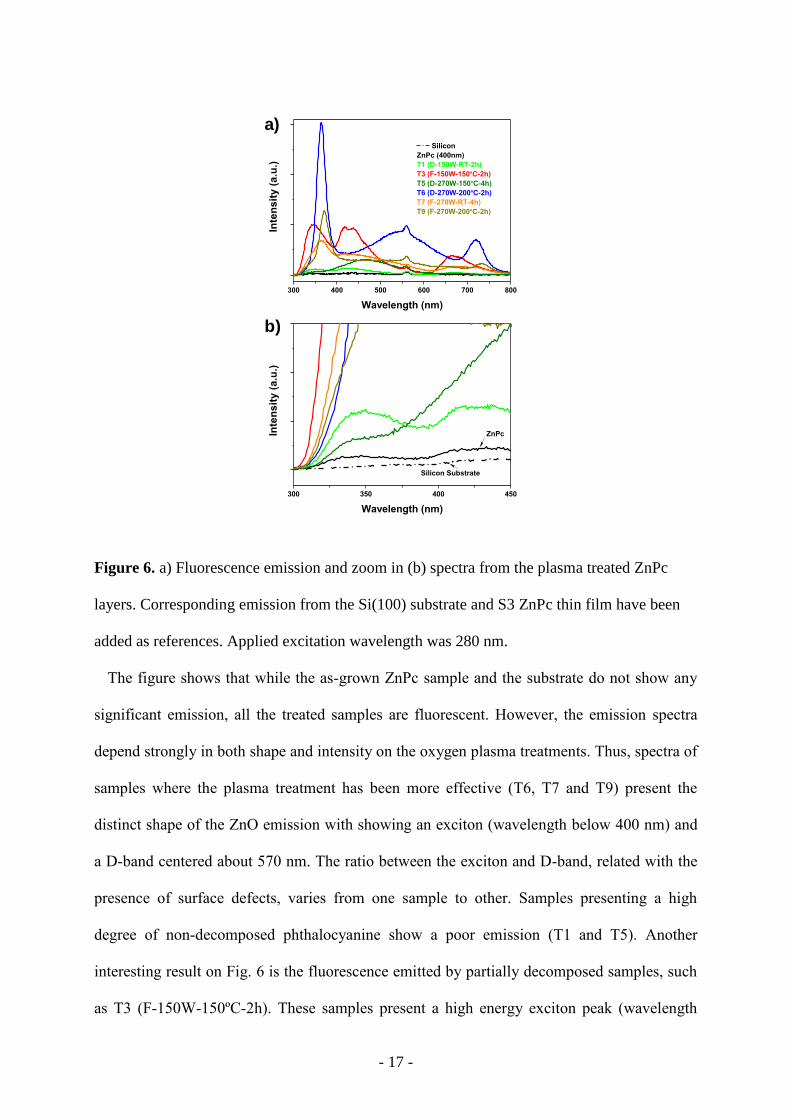
Figure 6 presents the fluorescence emission of selected ZnPc layers after
the different plasma treatments.
- 17 -
300 400 500 600 700 800
Inte
nsit
y (
a.u
.)
Wavelength (nm)
Silicon
ZnPc (400nm)
T1 (D-150W-RT-2h)
T3 (F-150W-150ºC-2h)
T5 (D-270W-150ºC-4h)
T6 (D-270W-200ºC-2h)
T7 (F-270W-RT-4h)
T9 (F-270W-200ºC-2h)
300 350 400 450
ZnPc
Inte
nsit
y (
a.u
.)
Wavelength (nm)
Silicon Substrate
a)
b)
Figure 6. a) Fluorescence emission and zoom in (b) spectra from the plasma treated ZnPc
layers. Corresponding emission from the Si(100) substrate and S3 ZnPc thin film have been
added as references. Applied excitation wavelength was 280 nm.
The figure shows that while the as-grown ZnPc sample and the substrate do not show any
significant emission, all the treated samples are fluorescent. However, the emission spectra
depend strongly in both shape and intensity on the oxygen plasma treatments. Thus, spectra of
samples where the plasma treatment has been more effective (T6, T7 and T9) present the
distinct shape of the ZnO emission with showing an exciton (wavelength below 400 nm) and
a D-band centered about 570 nm. The ratio between the exciton and D-band, related with the
presence of surface defects, varies from one sample to other. Samples presenting a high
degree of non-decomposed phthalocyanine show a poor emission (T1 and T5). Another
interesting result on Fig. 6 is the fluorescence emitted by partially decomposed samples, such
as T3 (F-150W-150ºC-2h). These samples present a high energy exciton peak (wavelength

- 18 -
below 350 nm) and a double band centered at 440 nm. A very similar emission has been
published very recently as consequence of the coupling between ZnO quantum dots deposited
on a graphene monolayer shell,38
and these system has been proposed for the fabrication of
white-light-emitting diodes.
Oxygen plasma etching of ZnPc single crystal nanowires
We have applied the same approach to the formation of ZnO 1D nanostructures by plasma
treatment of ZnPc single crystal nanowires. In this case, the plasma etching experiments were
carried out at room temperature in the down-face configuration (see Table 1). The main
reason behind the application of such soft conditions is to conserve part of the organic
nanowire as scaffolding of the ZnO shell. Figure S6 shows the comparison of the planar SEM
views of the as-grown and T´1 (D-270W-RT-1h) samples. At first sight the two samples
present a similar normal view, although in the case of the treated sample the density of NWs
appear to be slightly lower, exposing part of the substrate. However, contrary to the results
involving the thin film treatments, the higher magnification micrograph in Fig. S6 c) does not
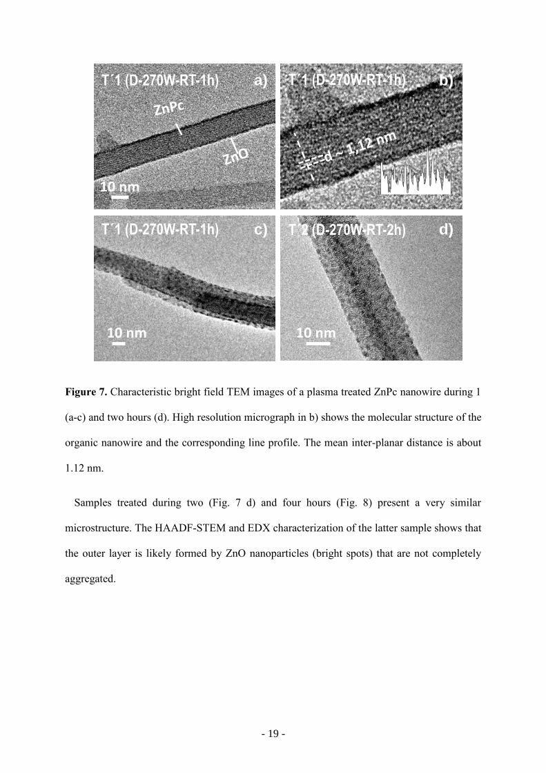
reveal any significant difference with respect to the as-grown samples (Fig. 1 f). Figure 7
gathers several bright field images of the samples after 1 and 2 hours of treatment showing
quite clearly the characteristic pattern corresponding to the arrangement of the ZnPc
molecules along the organic nanowire. An inter-planar distance of 1.12 nm is obtained from
the line profile in the Inset in Fig. 7 b), in good accordance with the molecule diameter and
results in the literature.39
This pattern appears surrounded by a darker shell formed by a
granulated layer as seen in panel c). The appearance of such layer is homogeneous along of
the nanowires, indicating a poor effect of the shadowing or self-shadowing factors under these
plasma conditions.
- 19 -
T�1 (D-270W-RT-1h) a)
10 nm
b)
10 nm
d)
2 4 6 8 10 12 14 16
10 nm
c)
T�1 (D-270W-RT-1h)
T�1 (D-270W-RT-1h) T�2 (D-270W-RT-2h)
Figure 7. Characteristic bright field TEM images of a plasma treated ZnPc nanowire during 1
(a-c) and two hours (d). High resolution micrograph in b) shows the molecular structure of the
organic nanowire and the corresponding line profile. The mean inter-planar distance is about
1.12 nm.
Samples treated during two (Fig. 7 d) and four hours (Fig. 8) present a very similar
microstructure. The HAADF-STEM and EDX characterization of the latter sample shows that
the outer layer is likely formed by ZnO nanoparticles (bright spots) that are not completely
aggregated.
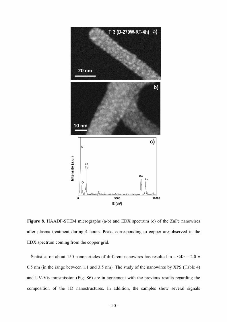
- 20 -
0 5000 10000
C
Zn
Cu
Inte
nsit
y (
a.u
.)
E (eV)
CuZn
O
10 nm
b)
20 nm
a)
c)
T�3 (D-270W-RT-4h)
Figure 8. HAADF-STEM micrographs (a-b) and EDX spectrum (c) of the ZnPc nanowires
after plasma treatment during 4 hours. Peaks corresponding to copper are observed in the
EDX spectrum coming from the copper grid.
Statistics on about 150 nanoparticles of different nanowires has resulted in a <d> ~ 2.0 ±
0.5 nm (in the range between 1.1 and 3.5 nm). The study of the nanowires by XPS (Table 4)
and UV-Vis transmission (Fig. S6) are in agreement with the previous results regarding the
composition of the 1D nanostructures. In addition, the samples show several signals

- 21 -
corresponding to the substrate (Au, Si and SiO2). The percentage of oxygen (%O) is affected
by O-Si and O-Au. The amount of N after both treatments is lower in comparison with the as-
grown ONWs. Thus, these results confirm the transformation of part of the ZnPc ONWs into
ZnO.
Table 4. Atomic percentages and ratios obtained by XPS for the as-grown and plasma treated
ZnPc nanowires.
SAMPLE % Zn % N % C % O
ZnPc ONWs 2.6 15.8 75.2 6.4
T´1 (D-270W-RT-1h) 3.1 7.7 69.5 19.7
T´3 (D-270W-RT-4h) 4.1 3.6 68.2 24.1
For short treatments (T’1, 1h) the ratio nitrogen to zinc differs slightly from the
corresponding to the ZnPc nanowires. In addition, the UV-Vis transmittance still presents the
well-defined B and Q bands at the same position as the as-grown sample. For the longest
treatment, i.e. 4 hours, the amount of oxygen increases significantly in the surface of the
nanowires at the same time that the content in nitrogen ratio drops below 4%. However, part
of the organic compound is still present as demonstrated by the corresponding UV-Vis
transmittance spectrum in Fig. S7 where the total transmission increases drastically in
comparison with the as-grown ONWs and sample T´1 (D-270W-RT-1h) at the same time that
the intensities of the B and Q bands decrease. This set of results might indicate that the soft
plasma conditions applied to the ZnPc nanowires produce, altogether to the ZnO grains shown
by TEM and HAADF-STEM (Fig. 7 and 8), a homogenous ZnO shell of reduced size. Even
for long runtime experiments, part of the Zn phthalocyanine remains as a core. The formation
of a ZnO shell that protects part of the ZnPc forming the core even for long exposition times
to the plasma is in good accordance with the results in the previous section for the plasma

- 22 -
treated thin films in the down-face conditions. In fact, if the results in nanowires are
extrapolated to the thin films then a composite microstructure might be claimed. Thus, under
soft-etching conditions, i.e. down-face configuration, the ZnO shell shields the organic
counterpart from the arrival of oxygen species from the plasma. In addition, the low
temperature operation reduces the mobility of the organic molecules slowing down the
conversion into zinc oxide.
Conclusion
We have demonstrated a versatile protocol for the formation of highly porous ZnO thin
films and nanowires by oxygen plasma treatment under different conditions of Zn-
phthalocyanine thin films and single-crystal nanowires correspondently. The ZnPc conversion
to ZnO is preferentially dominated by the geometry of the plasma and the substrate
temperature during the experiments. Thus, at mild substrate temperatures the ZnPc molecules
show a higher degree of mobility becoming much more easily oxidized. In a similar way, the
front-face operation increases the number of oxygen species reaching the surface of the
sample producing a faster formation of ZnO. Working in the front-face geometry allows the
complete transformation of ZnPc into ZnO for prolonged treatments even at room
temperature. It is therefore required treatments with the samples exposed to the plasma, high
temperature of the substrates and/or prolonged times in order to prompt the complete
conversion from ZnPc to ZnO. Highly porous ZnO thin films with surface coverages as low
as 55% can be produced by this method. Such a reduced density yields an extremely low
refractive index (n (550 nm) = 1.11) for an optical thickness of t = 135 nm. As far as we
know, this is one of the lowest refractive index reported for ZnO and opens the possibility of
applying these layers as antireflective coatings and in graded index multilayer systems. 40
Fluorescence emissions of the thin films are dominated by the exciton in the UV region. For

- 23 -
some of the samples the visible contribution related to surface defects is also presented. The
protocol has been exploited to fabricate ZnO decorated nanowires. Concretely, the 1D
nanostructure is form by a ZnPc core surrounded by ZnO nanoparticles with sizes in the range
between 1.1 and 3.5 nm. In this case, non-shadowing effects have been revealed after the
examination of the nanowires by electron microscopy techniques. It is worthy to mention
additional advantages of the use of the ZnPc as precursor material for the formation of ZnO as
its low toxicity and harmful in comparison to other organometallic precursors as diethyl zinc.
ZnPc sublimates at mild temperatures and the growth rate of the precursor layers is easily
tuned by varying the sample-evaporation cell distance and chamber pressure which allow
increasing the deposition yield. In addition, the method is directly expandable to wafer-scale
dimensions. Finally, it is interesting to stress that the method developed herein is
straightforwardly applicable to the fabrication of other metal oxide and metal porous materials
thanks to the ample variety available in the metal phthalocyanine and porphyrin precursors
and capability to tune the plasma oxidative / reductor character in remote operation.
Acknowledgements: We thank the Junta de Andalucia (TEP8067, FQM-196, and P12-
FQM-2265), the Spanish Ministry of Economy and Competitiveness (MAT2013-40852-R,
MAT2013-42900-P and RECUPERA 2020), EU (project grant number REGPOT-CT-2011-
285895-Al-NANOFUNC) and Abengoa Research S. L. (Framework Project) for financial
support.
Received: ((will be filled in by the editorial staff)); Revised: ((will be filled in by the editorial
staff)); Published online: ((please add journal code and manuscript number, e.g., DOI:
10.1002/ppap.201100001))

- 24 -
Keywords: nanowires; phthalocyanine; plasma etching; porous films; ZnO
[1] Z. L. Wang, Mat. Sci. Eng. R 2009, 64, 33.
[2] A. B. Djurisic, Y.H., Leung, Small 2006, 2, 944.
[3] Y. Tak, K. Yong, C. Park, J. Electrochem. Soc. 2005, 152, 794.
[4] M. Haupt, A. Ladenburger, R. Sauer, K. Thonke, R. Glass, W. Roos, J.P. Spatz, H.
Rauscher, S. Riethmüller, M. Möller, J. Appl. Phys. 2003, 93, 6252.
[5] D. Ito, M. L. Jespersen, J. E. Hutchison, Acs Nano. 2008, 2, 2001.
[6] J. Elias, R. Tena-Zaera, G.Y. Wang, C. Lévy-Clément, Chem. Mater. 2008, 20, 6633.
[7] W.Y. Wu, J. M. Ting, P. J. Huang, Nanoscale Res. Lett. 2009, 4, 513.
[8] M. H. Huang, S. Mao, H. Feick, H. Yan, Y. Wu, H. Kind, E. Weber, R. Russo, P.
Yang, Science 2001, 292, 1897.
[9] a) M. Law, L. E. Greene, J. C. Johnson, R. Saykally, P. Yang, Nat. Mater. 2005, 4,
455; b) A. G. Vega-Poot, M. Macias-Montero, J. Idigoras, A. Borras, A. Barranco, A. R.
Gonzalez-Elipe, F. I. Lizama-Tzec, G. Oskam, J. A. Anta, ChemPhysChem 2014, 15, 1088;
c) J. S. Woo, G. E. Jang, Trans. Electric. Electron. Mater. 2015, 14, 312.
[10] H. Koga, T. Kitaoka, H. Wariishi, J. of Mater. Chem. 2009, 19, 2135.
[11] S. G. Kumar, K. S. Rao, RSC Adv. 2015, 5, 3306.
[12] J. L. Campbell, M. Breedon, K. Latham, K. Kalantar-zadeh, Langmuir 2008, 24, 5091.
[13] X. Feng, L. Feng, M. Jin, J. Zhai, L. Jiang, D. Zhu, J. Am. Chem. Soc. 2004, 126, 62.

- 25 -
[14] S. H. Ko, D. Lee, H. W. Kang, K. H. Nam, J. Y. Yeo, S. J. Hong, C. P.
Grigoropoulos, H. J. Sung, H. J., Nano Lett. 2011, 11, 666.
[15] Y. Sun, N. George Ndifor-Angwafor, D. Jason Riley, M. N. R. Ashfold, Chem. Phys.
Lett. 2006, 431, 352.
[16] K. H. Tam, C. K. Cheung, Y. H. Leung, A. B. Djurisic, C. C. Ling, C. D. Beling, S.
Fung, W. M. Kwok, W. K. Chan, D. L. Phillips, L. Ding, W. K. Ge, J. Phys. Chem. B. 2006,
110, 20865.
[17] M. Guo, P. Diao, S. Cai, J. Solid State Chem. 2005, 178, 1864.
[18] M. H. Huang, S. Mao, H. Feick, H. Q. Yan, Y. Y. Wu, H. Kind, E. Weber, R. Russo,
P. D. Yang. Science. 2001, 292, 1897.
[19] Y. Wu, P. Yang, Chem. Mater. 2000, 12, 605.
[20] Y. Wu, P. Yang, J. Am. Chem. Soc. 2001, 123, 3165.
[21] M. H. Huang, Y. Wu, H. Feick, N. Tran, E. Weber, P. Yang, Adv. Mater. 2001, 13,
113.
[22] P. Yang, H. Yan, S. Mao, R. Russo, J. Johnson, R. Saykally, N. Morris, J. Pham, R.
He, H. J. Choi, Adv. Funct. Mater. 2002, 12, 323.
[23] S. J. Pearton, D. P. Norton, K. Ip, Y. W. Heo, T. Steiner, J. Vac. Sci. Technol. B 2004,
22, 932.
[24] W. Z. Xu, Z. Z. Ye, Y. J. Zeng, L. P. Zhu, B. H. Zhao, L. Jiang, J. G. Lu, H. P. He, S.
B. Zhang, Appl. Phys. Lett. 2006, 88, 17350.
[25] D. Barreca, D. Bekermann, E. Comini, A. Devi, R. A. Fischer, A. Gasparotto, C.
Maccato, G. Sberveglieri, E. Tondello, Sens. Actuators B. 2010, 149, 1.
- 26 -
[26] W. T. Zheng, Y. M. Ho, H. W. Tian, M. Wen, J. L. Qi, Y. A. Li, J. Phys. Chem. C
2009, 113, 9164.
[27] P. Romero-Gomez, J. Toudert, J. R. Sanchez-Valencia, A. Borras, A. Barranco, A. R.
Gonzalez-Elipe, J. Phys. Chem. C 2010, 114, 20932.
[28] M. Macias-Montero, A. Borras, Z. Saghi, P. Romero-Gomez, J. R. Sanchez-Valencia,
J. C. Gonzalez, A. Barranco, P. Midgley, J. Cotrino, A. R. Gonzalez-Elipe, J. Mater. Chem.
2012, 22, 1341.
[29] J. R. Sanchez-Valencia, M. Alcaire, P. Romero-Gómez, M. Macias-Montero, F. J.
Aparicio, A. Borras, A. R. Gonzalez-Elipe, A. Barranco, J. Phys. Chem. C. 2014, 118, 9852.
[30] R. J. Chung, Z. C. Lin, C. A. Lin, K. Y. Lai, Thin Solid Films. 2014, 570, 504.
[31] S. Aydemir, S. Karakaya, J. Magn. Magn. Mater. 2015, 373, 33.
[32] A. Zawadzka, P. Płóciennik, J. Strzelecki, B. Sahraoui, Opt. Mater. 2014, 37, 327.
[33] M. Alcaire, J. R. Sanchez-Valencia, F. J. Aparicio, Z. Saghi, J. C. Gonzalez-Gonzalez,
A. Barranco, Y. O. Zian, A. R. Gonzalez-Elipe, P. Midgley, J. P. Espinos, P. Groening, A.
Borras, Nanoscale. 2011, 3, 4554.
[34] NIST X-ray Photoelectron Spectroscopy Database.
http://srdata.nist.gov/xps/Default.aspx
[35] a) M. Macias-Montero, A. N. Filippin, Z. Saghi, F. J. Aparicio, A. Barranco, J. P.
Espinos, F. Frutos, A. R. Gonzalez-Elipe, A. Borras, Adv. Funct. Mater. 2013, 23, 5981; b) A.
Borras, O. Groening, M. Aguirre, F. Gramm, P. Groning, Langmuir. 2010, 26, 5763; c) A.
Borras, O. Groening, , J. Koeble, P. Groening, Adv. Mater. 2009, 21, 4816; d) A. Borras, M.
Aguirre, O. Groening, C. Lopez-Cartes, P. Groening, Chem. Mater. 2008, 20, 7371.

- 27 -
[36] S. Senthilarasu, Y. B. Hahn, S. H. Lee, J. Mater. Sci: Mater. Electron. 2008, 19, 482.
[37] İ. Özçeşmeci, I. Sorar, A. Gül, Inorg. Chem. Commun. 2011, 14, 1254.
[38] D. I. Son, B. W. Kwon, D. H. Park, W. S. Seo, Y. Yi, B. Angadi, C. L. Lee, W. K.
Choi, Nat. Nano. 2012, 7, 465.
[39] H. K. Moon, M. Son, J. E. Park, S. M. Yoon, S. H. Lee, H. C. Choi, NPG Asia Mater.
2012, 4, 12.
[40] J. Q. Xi, M. F. Schubert, J. K. Kim, E. F. Schubert, M. Chen, S. Y. Lin, W. Liu, Nat.
Photon. 2007, 1, 176.
A vacuum protocol is presented for the fabrication of highly porous 2D and 1D
nanostructures based on the plasma oxidation of Zn-phthalocyanine precursor layers
previously formed by physical vapor deposition. Luminescent antireflective coatings of
ZnO are achieved. The method developed is straightforwardly extendable to the fabrication of
other metal oxide and metal porous materials thanks to the ample variety in the metal
phthalocyanine precursors.
M. Alcaire, A. N. Filippin, M. Macias-Montero, J. R. Sanchez-Valencia, T. C. Rojas, A.
Mora-Boza, C. Lopez-Santos, J.P. Espinos, A. Barranco and A. Borras *
Highly porous ZnO thin films and 1D nanostructures by remote plasma processing of
Zn-phthalocyanine