Highe-Speed CMOS Logic Quad Bilateral Switch … · Implications of Slow or Floating CMOS Inputs,...
16
CD74HCT4066-Q1 HIGH-SPEED CMOS LOGIC QUAD BILATERAL SWITCH SCLS581B - APRIL 2004 - REVISED APRIL 2008 1 POST OFFICE BOX 655303 • DALLAS, TEXAS 75265 D Qualified for Automotive Applications D Low ON Resistance - 25 W Typical (V CC = 4.5 V) D Fast Switching and Propagation Speeds D Low OFF Leakage Current D Wide Operating Temperature Range: -405C to 1255C D Direct LSTTL Input Logic Compatibility: V IL = 0.8 V Max, V IH = 2 V Min D CMOS Input Compatibility: I I v 1 mA at V OL , V OH description/ordering information The CD74HCT4066 contains four independent digitally controlled analog switches that use silicon-gate CMOS technology to achieve operation speeds similar to LSTTL, with the low power consumption of standard CMOS integrated circuits. These switches feature the characteristic linear ON resistance of the metal-gate CD4066B. Each switch is turned on by a high-level voltage on its control input. ORDERING INFORMATION { T A PACKAGE ‡ ORDERABLE PART NUMBER § TOP-SIDE MARKING 40°C to 125°C SOIC - M Reel of 2500 CD74HCT4066QM96Q1 HCT4066Q -40°C to 125°C TSSOP - PW Reel of 2000 CD74HCT4066QPWRQ1 HK4066Q † For the most current package and ordering information, see the Package Option Addendum at the end of this document, or see the TI web site at http://www.ti.com. ‡ Package drawings, thermal data, and symbolization are available at http://www.ti.com/packaging. § The suffix 96 denotes tape and reel. FUNCTION TABLE INPUT SWITCH INPUT nE SWITCH L Off H On H = High level L = Low level Copyright 2008, Texas Instruments Incorporated PRODUCTION DATA information is current as of publication date. Products conform to specifications per the terms of Texas Instruments standard warranty. Production processing does not necessarily include testing of all parameters. Please be aware that an important notice concerning availability, standard warranty, and use in critical applications of Texas Instruments semiconductor products and disclaimers thereto appears at the end of this data sheet. M OR PW PACKAGE (TOP VIEW) 1 2 3 4 5 6 7 14 13 12 11 10 9 8 1Y 1Z 2Z 2Y 2E 3E GND V CC 1E 4E 4Y 4Z 3Z 3Y
Transcript of Highe-Speed CMOS Logic Quad Bilateral Switch … · Implications of Slow or Floating CMOS Inputs,...

CD74HCT4066-Q1HIGH-SPEED CMOS LOGICQUAD BILATERAL SWITCH
SCLS581B − APRIL 2004 − REVISED APRIL 2008
1POST OFFICE BOX 655303 • DALLAS, TEXAS 75265
Qualified for Automotive Applications
Low ON Resistance− 25 Typical (VCC = 4.5 V)
Fast Switching and Propagation Speeds
Low OFF Leakage Current
Wide Operating Temperature Range: −40Cto 125C
Direct LSTTL Input Logic Compatibility: VIL = 0.8 V Max, VIH = 2 V Min
CMOS Input Compatibility: II 1 A at VOL,VOH
description/ordering information
The CD74HCT4066 contains four independentdigitally controlled analog switches that usesilicon-gate CMOS technology to achieve operationspeeds similar to LSTTL, with the low powerconsumption of standard CMOS integrated circuits.
These switches feature the characteristic linear ONresistance of the metal-gate CD4066B. Each switchis turned on by a high-level voltage on its controlinput.
ORDERING INFORMATION
TA PACKAGE‡ ORDERABLEPART NUMBER§
TOP-SIDEMARKING
40°C to 125°CSOIC − M Reel of 2500 CD74HCT4066QM96Q1 HCT4066Q
−40°C to 125°CTSSOP − PW Reel of 2000 CD74HCT4066QPWRQ1 HK4066Q
† For the most current package and ordering information, see the Package Option Addendum at the endof this document, or see the TI web site at http://www.ti.com.
‡ Package drawings, thermal data, and symbolization are available at http://www.ti.com/packaging.§ The suffix 96 denotes tape and reel.
FUNCTION TABLE
INPUTSWITCH
INPUTnE
SWITCH
L Off
H On
H = High levelL = Low level
Copyright 2008, Texas Instruments IncorporatedPRODUCTION DATA information is current as of publication date.Products conform to specifications per the terms of Texas Instrumentsstandard warranty. Production processing does not necessarily includetesting of all parameters.
Please be aware that an important notice concerning availability, standard warranty, and use in critical applications ofTexas Instruments semiconductor products and disclaimers thereto appears at the end of this data sheet.
M OR PW PACKAGE(TOP VIEW)
1
2
3
4
5
6
7
14
13
12
11
10
9
8
1Y1Z2Z2Y2E3E
GND
VCC
1E4E4Y4Z3Z3Y
CD74HCT4066-Q1HIGH-SPEED CMOS LOGICQUAD BILATERAL SWITCHSCLS581B − APRIL 2004 − REVISED APRIL 2008
2 POST OFFICE BOX 655303 • DALLAS, TEXAS 75265
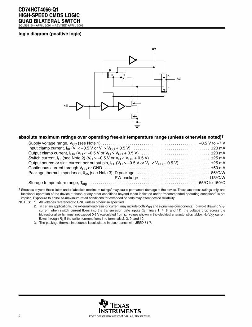
logic diagram (positive logic)
nY
nZ
nE
p
np
n
absolute maximum ratings over operating free-air temperature range (unless otherwise noted)†
Supply voltage range, VCC (see Note 1) −0.5 V to +7 V. . . . . . . . . . . . . . . . . . . . . . . . . . . . . . . . . . . . . . . . . . . . . . Input clamp current, IIK (VI < −0.5 V or VI > VCC + 0.5 V) ±20 mA. . . . . . . . . . . . . . . . . . . . . . . . . . . . . . . . . . . . . Output clamp current, IOK (VO < −0.5 V or VO > VCC + 0.5 V) ±20 mA. . . . . . . . . . . . . . . . . . . . . . . . . . . . . . . . . Switch current, IO (see Note 2) (VO > −0.5 V or VO < VCC + 0.5 V) ±25 mA. . . . . . . . . . . . . . . . . . . . . . . . . . . . Output source or sink current per output pin, IO (VO > −0.5 V or VO < VCC + 0.5 V) ±25 mA. . . . . . . . . . . . . . Continuous current through VCC or GND ±50 mA. . . . . . . . . . . . . . . . . . . . . . . . . . . . . . . . . . . . . . . . . . . . . . . . . . . Package thermal impedance, θJA (see Note 3): D package 86°C/W. . . . . . . . . . . . . . . . . . . . . . . . . . . . . . . . . . .
PW package 113°C/W. . . . . . . . . . . . . . . . . . . . . . . . . . . . . . . . Storage temperature range, Tstg −65°C to 150°C. . . . . . . . . . . . . . . . . . . . . . . . . . . . . . . . . . . . . . . . . . . . . . . . . . .
† Stresses beyond those listed under “absolute maximum ratings” may cause permanent damage to the device. These are stress ratings only, andfunctional operation of the device at these or any other conditions beyond those indicated under “recommended operating conditions” is notimplied. Exposure to absolute-maximum-rated conditions for extended periods may affect device reliability.
NOTES: 1. All voltages referenced to GND unless otherwise specified.2. In certain applications, the external load-resistor current may include both VCC and signal-line components. To avoid drawing VCC
current when switch current flows into the transmission gate inputs (terminals 1, 4, 8, and 11), the voltage drop across thebidirectional switch must not exceed 0.6 V (calculated from ron values shown in the electrical characteristics table). No VCC currentflows through RL if the switch current flows into terminals 2, 3, 9, and 10.
3. The package thermal impedance is calculated in accordance with JESD 51-7.

CD74HCT4066-Q1HIGH-SPEED CMOS LOGICQUAD BILATERAL SWITCH
SCLS581B − APRIL 2004 − REVISED APRIL 2008
3POST OFFICE BOX 655303 • DALLAS, TEXAS 75265
recommended operating conditions (see Note 4)
MIN MAX UNIT
VCC Supply voltage 4.5 5.5 V
VIH High-level input voltage 2 V
VIL Low-level input voltage 0.8 V
VI Input voltage 0 VCC V
VO Output voltage 0 VCC V
tt Input transition (rise and fall) time VCC = 4.5 V 0 500 ns
TA Operating free-air temperature −40 125 °C
NOTES: 4. All unused inputs of the device must be held at VCC or GND to ensure proper device operation. Refer to the TI application report,Implications of Slow or Floating CMOS Inputs, literature number SCBA004.
electrical characteristics over recommended operating free-air temperature range (unlessotherwise noted)
PARAMETER TEST CONDITIONS VI VCCTA = 25°C
TA = −40°CTO 125°C UNITPARAMETER TEST CONDITIONS VI VCC
MIN TYP MAX MIN MAXUNIT
IIL Any controlVCCor
GND5.5 V ±0.1 ±1 µA
IIZ VIS = VCC or GND VIL 5.5 V ±0.1 ±1 µA
rIO = 1 mA, VIS = VCC or GND VCC 4.5 V 25 80 128
ΩronIO = 1 mA, See Figure 7 VIS = VCC to GND VCC 4.5 V 35 95 142
Ω
∆ron Between any two switches VCC 4.5 V 1 Ω
ICC
VCCor
GND5.5 V 2 40 µA
∆ICCPer input pin: 1 unit load,See Note 5
VCC −2.1 V
4.5 Vto
5.5 V100 360 490 µA
CI Control inputs 10 10 pF
NOTE 5: For dual-supply systems, theoretical worst case (VI = 2.4 V, VCC = 5.5 V) specification is 1.8 mA.
HCT input loading
INPUT UNIT LOADS†
All 1† Unit load is ∆ICC limit specified in the electrical
characteristics table, e.g., 360 µA max at 25°C.

CD74HCT4066-Q1HIGH-SPEED CMOS LOGICQUAD BILATERAL SWITCHSCLS581B − APRIL 2004 − REVISED APRIL 2008
4 POST OFFICE BOX 655303 • DALLAS, TEXAS 75265
switching characteristics over recommended operating free-air temperature range (unlessotherwise noted) (see Figure 6)
PARAMETERFROM
(INPUT)TO
(OUTPUT)LOAD
CAPACITANCEVCC
TA = 25°CTA = −40°CTO 125°C UNITPARAMETER
(INPUT) (OUTPUT) CAPACITANCEVCC
MIN TYP MAX MIN MAXUNIT
t Y or Z Z or YCL = 15 pF 5 V 4
nstpd Y or Z Z or YCL = 50 pF 4.5 V 12 18
ns
t E Y or ZCL = 15 pF 5 V 9
nsten E Y or ZCL = 50 pF 4.5 V 24 36
ns
t E Y or ZCL = 15 pF 5 V 14
nstdis E Y or ZCL = 50 pF 4.5 V 35 53
ns
operating characteristics, VCC = 5 V, TA = 25°C, input tr, tf = 6 ns
PARAMETER TYP UNIT
Cpd Power dissipation capacitance (see Note 6) 38 pF
NOTE 6: Cpd is used to determine the dynamic power consumption (PD), per package.PD = (Cpd × VCC
2 × fI) + Σ (CL + CS) × VCC2 × fO
fO = output frequencyfI = input frequencyCL = output load capacitanceCS = switch capacitanceVCC = supply voltage
analog channel characteristics, TA = 25°CPARAMETER TEST CONDITIONS VCC TYP UNIT
fmax Switch frequency response bandwidth at −3 dB See Figure 2 and Figure 8 and Notes 7 and 8 4.5 V 200 MHz
Crosstalk between any two switches See Figure 1 and Figure 9 and Notes 8 and 9 4.5 V −72 dB
Total harmonic distortion See Figure 3, 1 kHz, VIS = 4 VP-P 4.5 V 0.023 %
Control to switch feedthrough noise See Figure 4 4.5 V 130 mV
Switch OFF signal feedthrough See Figure 5 and Figure 9 and Notes 8 and 9 4.5 V −72 dB
CS Switch input capacitance 5 pF
NOTES: 7. Adjust input voltage to obtain 0 dBm at output, f = 1 MHz.8. VIS is centered at VCC/2.9. Adjust input for 0 dBm at VIS.

CD74HCT4066-Q1HIGH-SPEED CMOS LOGICQUAD BILATERAL SWITCH
SCLS581B − APRIL 2004 − REVISED APRIL 2008
5POST OFFICE BOX 655303 • DALLAS, TEXAS 75265
PARAMETER MEASUREMENT INFORMATION
Figure 1. Crosstalk Between Two Switches Test Circuit
SWITCHON
VCC
VCC/2
0.1 F
VIS
VOS1
R C
SWITCHOFF
dBMETER
VCC
VCC/2
VOS2R
VCC/2R C
R
INPUT
fIS = 1-MHz Sine WaveR = 50 C = 10 pF
Figure 2. Frequency-Response Test Circuit
50 Ω 10 pF
SWITCHON
dBMETER
VCC
VCC/2
0.1 F
VIS
VOS
Figure 3. Total Harmonic Distortion Test Circuit
10k Ω 50 pF
SWITCHON
DISTORTIONMETER
VCC
VCC/2
10 F
SineWave
VISVOS
VISVI = VIH
fIS = 1 kHz to 10 kHz
Figure 4. Control-to-Switch Feedthrough NoiseTest Circuit
600 Ω 50 pF
VOS
600 Ω
VOS
VP−P
E
SCOPE
SWITCHALTERNATINGON AND OFF
tr, tf ≤ 6 nsfCONT = 1 MHz
50% DUTYCYCLE
VCC
VCC/2
VCC/2
Figure 5. Switch OFF Signal FeedthroughTest Circuit
VIS
0.1 µF
R C
VOS
R
VCC
VCC/2VCC/2
fIS ≥ 1-MHz Sine WaveR = 50 ΩC = 10 pF
VC = VSWITCH
OFF
dB
METER
IL

CD74HCT4066-Q1HIGH-SPEED CMOS LOGICQUAD BILATERAL SWITCHSCLS581B − APRIL 2004 − REVISED APRIL 2008
6 POST OFFICE BOX 655303 • DALLAS, TEXAS 75265
PARAMETER MEASUREMENT INFORMATION
TestPointFrom Output
Under Test
CL(see Note A)
VCC
S1
S2
LOAD CIRCUIT
PARAMETER
tPZH
tpd
tdis
tentPZL
tPHZ
tPLZ
Open Closed
S1
Closed Open
S2
Open Closed
Closed Open
Open Open
NOTES: A. CL includes probe and test-fixture capacitance.B. Waveform 1 is for an output with internal conditions such that the output is low, except when disabled by the output control.
Waveform 2 is for an output with internal conditions such that the output is high, except when disabled by the output control.C. Phase relationships between waveforms were chosen arbitrarily. All input pulses are supplied by generators having the following
characteristics: PRR ≤ 1 MHz, ZO = 50 Ω, tr = 6 ns, tf = 6 ns.D. For clock inputs, fmax is measured with the input duty cycle at 50%.E. The outputs are measured one at a time, with one input transition per measurement.F. tPLZ and tPHZ are the same as tdis.G. tPZL and tPZH are the same as ten.H. tPLH and tPHL are the same as tpd.
RL = 1 kΩ
VOLTAGE WAVEFORMSPROPAGATION DELAY AND OUTPUT TRANSITION TIMES
1.3 V
1.3 V1.3 V10%
90% 90%
3 V
VOH
VOL
0 V
tr tf
Input
In-PhaseOutput
1.3 V
tPLH tPHL
1.3 V 1.3 V10%
90%90%VOH
VOLtrtf
tPHL tPLH
Out-of-PhaseOutput
OutputControl
OutputWaveform 1(see Note B)
OutputWaveform 2(see Note B)
VOL
VOH
tPZL
tPZH
tPLZ
tPHZ
≈VCC
0 V
1.3 V10%
1.3 V≈0 V
VOLTAGE WAVEFORMSOUTPUT ENABLE AND DISABLE TIMES
1.3 V 1.3 V
90%
3 V
10%
10%
Figure 6. Load Circuit and Voltage Waveforms

CD74HCT4066-Q1HIGH-SPEED CMOS LOGICQUAD BILATERAL SWITCH
SCLS581B − APRIL 2004 − REVISED APRIL 2008
7POST OFFICE BOX 655303 • DALLAS, TEXAS 75265
TYPICAL CHARACTERISTICS
Input Signal Voltage − V
ON
Res
ista
nce
−Ω
Figure 7. Typical ON Resistance vs Input Signal Voltage
50
40
30
20
10
1 2 3 4 5 6 7 8 9
VCC = 4.5 V, PIN 1 TO 2
4.5
60
0
TA = 25CGND = 0 V
104 105 106 107 108Frequency − Hz
Ch
ann
el-O
N B
and
wid
th −
dB
Figure 8. Switch Frequency Response, VCC = 4.5 V
−1
−2
−3
−4
0
CL = 10 pFVCC = 4.5 VRL = 50 ΩTA = 25CPin 4 to 3
1
104 105 106 107 108
Figure 9. Switch-OFF Signal Feedthrough andCrosstalk vs Frequency, VCC = 4.5 V
Cro
ssta
lk −
dB
f − Frequency − Hz
Sw
itch
-Off
Sig
nal
Fee
dth
rou
gh
− d
B CL = 10 pFVCC = 4.5 VRL = 50 ΩTA = 25CPin 4 to 3
−80
−100
−20
0
−40
−60

PACKAGE OPTION ADDENDUM
www.ti.com 11-Apr-2013
Addendum-Page 1
PACKAGING INFORMATION
Orderable Device Status(1)
Package Type PackageDrawing
Pins PackageQty
Eco Plan(2)
Lead/Ball Finish MSL Peak Temp(3)
Op Temp (°C) Top-Side Markings(4)
Samples
CD74HCT4066QM96Q1 ACTIVE SOIC D 14 2500 Green (RoHS& no Sb/Br)
CU NIPDAU Level-1-260C-UNLIM -40 to 125 HCT4066Q
CD74HCT4066QPWRQ1 ACTIVE TSSOP PW 14 2000 Green (RoHS& no Sb/Br)
CU NIPDAU Level-1-260C-UNLIM -40 to 125 HK4066Q
D24066QM96G4Q1 ACTIVE SOIC D 14 2500 Green (RoHS& no Sb/Br)
CU NIPDAU Level-1-260C-UNLIM -40 to 125 HCT4066Q
HCT4066QPWRG4Q1 ACTIVE TSSOP PW 14 2000 Green (RoHS& no Sb/Br)
CU NIPDAU Level-1-260C-UNLIM -40 to 125 HK4066Q
(1) The marketing status values are defined as follows:ACTIVE: Product device recommended for new designs.LIFEBUY: TI has announced that the device will be discontinued, and a lifetime-buy period is in effect.NRND: Not recommended for new designs. Device is in production to support existing customers, but TI does not recommend using this part in a new design.PREVIEW: Device has been announced but is not in production. Samples may or may not be available.OBSOLETE: TI has discontinued the production of the device.
(2) Eco Plan - The planned eco-friendly classification: Pb-Free (RoHS), Pb-Free (RoHS Exempt), or Green (RoHS & no Sb/Br) - please check http://www.ti.com/productcontent for the latest availabilityinformation and additional product content details.TBD: The Pb-Free/Green conversion plan has not been defined.Pb-Free (RoHS): TI's terms "Lead-Free" or "Pb-Free" mean semiconductor products that are compatible with the current RoHS requirements for all 6 substances, including the requirement thatlead not exceed 0.1% by weight in homogeneous materials. Where designed to be soldered at high temperatures, TI Pb-Free products are suitable for use in specified lead-free processes.Pb-Free (RoHS Exempt): This component has a RoHS exemption for either 1) lead-based flip-chip solder bumps used between the die and package, or 2) lead-based die adhesive used betweenthe die and leadframe. The component is otherwise considered Pb-Free (RoHS compatible) as defined above.Green (RoHS & no Sb/Br): TI defines "Green" to mean Pb-Free (RoHS compatible), and free of Bromine (Br) and Antimony (Sb) based flame retardants (Br or Sb do not exceed 0.1% by weightin homogeneous material)
(3) MSL, Peak Temp. -- The Moisture Sensitivity Level rating according to the JEDEC industry standard classifications, and peak solder temperature.
(4) Multiple Top-Side Markings will be inside parentheses. Only one Top-Side Marking contained in parentheses and separated by a "~" will appear on a device. If a line is indented then it is acontinuation of the previous line and the two combined represent the entire Top-Side Marking for that device.
Important Information and Disclaimer:The information provided on this page represents TI's knowledge and belief as of the date that it is provided. TI bases its knowledge and belief on informationprovided by third parties, and makes no representation or warranty as to the accuracy of such information. Efforts are underway to better integrate information from third parties. TI has taken andcontinues to take reasonable steps to provide representative and accurate information but may not have conducted destructive testing or chemical analysis on incoming materials and chemicals.TI and TI suppliers consider certain information to be proprietary, and thus CAS numbers and other limited information may not be available for release.
In no event shall TI's liability arising out of such information exceed the total purchase price of the TI part(s) at issue in this document sold by TI to Customer on an annual basis.

PACKAGE OPTION ADDENDUM
www.ti.com 11-Apr-2013
Addendum-Page 2
OTHER QUALIFIED VERSIONS OF CD74HCT4066-Q1 :
• Catalog: CD74HCT4066
NOTE: Qualified Version Definitions:
• Catalog - TI's standard catalog product

TAPE AND REEL INFORMATION
*All dimensions are nominal
Device PackageType
PackageDrawing
Pins SPQ ReelDiameter
(mm)
ReelWidth
W1 (mm)
A0(mm)
B0(mm)
K0(mm)
P1(mm)
W(mm)
Pin1Quadrant
CD74HCT4066QPWRQ1 TSSOP PW 14 2000 330.0 12.4 6.9 5.6 1.6 8.0 12.0 Q1
HCT4066QPWRG4Q1 TSSOP PW 14 2000 330.0 12.4 6.9 5.6 1.6 8.0 12.0 Q1
PACKAGE MATERIALS INFORMATION
www.ti.com 22-Jan-2015
Pack Materials-Page 1

*All dimensions are nominal
Device Package Type Package Drawing Pins SPQ Length (mm) Width (mm) Height (mm)
CD74HCT4066QPWRQ1 TSSOP PW 14 2000 367.0 367.0 35.0
HCT4066QPWRG4Q1 TSSOP PW 14 2000 367.0 367.0 35.0
PACKAGE MATERIALS INFORMATION
www.ti.com 22-Jan-2015
Pack Materials-Page 2


IMPORTANT NOTICE
Texas Instruments Incorporated and its subsidiaries (TI) reserve the right to make corrections, enhancements, improvements and otherchanges to its semiconductor products and services per JESD46, latest issue, and to discontinue any product or service per JESD48, latestissue. Buyers should obtain the latest relevant information before placing orders and should verify that such information is current andcomplete. All semiconductor products (also referred to herein as “components”) are sold subject to TI’s terms and conditions of salesupplied at the time of order acknowledgment.TI warrants performance of its components to the specifications applicable at the time of sale, in accordance with the warranty in TI’s termsand conditions of sale of semiconductor products. Testing and other quality control techniques are used to the extent TI deems necessaryto support this warranty. Except where mandated by applicable law, testing of all parameters of each component is not necessarilyperformed.TI assumes no liability for applications assistance or the design of Buyers’ products. Buyers are responsible for their products andapplications using TI components. To minimize the risks associated with Buyers’ products and applications, Buyers should provideadequate design and operating safeguards.TI does not warrant or represent that any license, either express or implied, is granted under any patent right, copyright, mask work right, orother intellectual property right relating to any combination, machine, or process in which TI components or services are used. Informationpublished by TI regarding third-party products or services does not constitute a license to use such products or services or a warranty orendorsement thereof. Use of such information may require a license from a third party under the patents or other intellectual property of thethird party, or a license from TI under the patents or other intellectual property of TI.Reproduction of significant portions of TI information in TI data books or data sheets is permissible only if reproduction is without alterationand is accompanied by all associated warranties, conditions, limitations, and notices. TI is not responsible or liable for such altereddocumentation. Information of third parties may be subject to additional restrictions.Resale of TI components or services with statements different from or beyond the parameters stated by TI for that component or servicevoids all express and any implied warranties for the associated TI component or service and is an unfair and deceptive business practice.TI is not responsible or liable for any such statements.Buyer acknowledges and agrees that it is solely responsible for compliance with all legal, regulatory and safety-related requirementsconcerning its products, and any use of TI components in its applications, notwithstanding any applications-related information or supportthat may be provided by TI. Buyer represents and agrees that it has all the necessary expertise to create and implement safeguards whichanticipate dangerous consequences of failures, monitor failures and their consequences, lessen the likelihood of failures that might causeharm and take appropriate remedial actions. Buyer will fully indemnify TI and its representatives against any damages arising out of the useof any TI components in safety-critical applications.In some cases, TI components may be promoted specifically to facilitate safety-related applications. With such components, TI’s goal is tohelp enable customers to design and create their own end-product solutions that meet applicable functional safety standards andrequirements. Nonetheless, such components are subject to these terms.No TI components are authorized for use in FDA Class III (or similar life-critical medical equipment) unless authorized officers of the partieshave executed a special agreement specifically governing such use.Only those TI components which TI has specifically designated as military grade or “enhanced plastic” are designed and intended for use inmilitary/aerospace applications or environments. Buyer acknowledges and agrees that any military or aerospace use of TI componentswhich have not been so designated is solely at the Buyer's risk, and that Buyer is solely responsible for compliance with all legal andregulatory requirements in connection with such use.TI has specifically designated certain components as meeting ISO/TS16949 requirements, mainly for automotive use. In any case of use ofnon-designated products, TI will not be responsible for any failure to meet ISO/TS16949.
Products ApplicationsAudio www.ti.com/audio Automotive and Transportation www.ti.com/automotiveAmplifiers amplifier.ti.com Communications and Telecom www.ti.com/communicationsData Converters dataconverter.ti.com Computers and Peripherals www.ti.com/computersDLP® Products www.dlp.com Consumer Electronics www.ti.com/consumer-appsDSP dsp.ti.com Energy and Lighting www.ti.com/energyClocks and Timers www.ti.com/clocks Industrial www.ti.com/industrialInterface interface.ti.com Medical www.ti.com/medicalLogic logic.ti.com Security www.ti.com/securityPower Mgmt power.ti.com Space, Avionics and Defense www.ti.com/space-avionics-defenseMicrocontrollers microcontroller.ti.com Video and Imaging www.ti.com/videoRFID www.ti-rfid.comOMAP Applications Processors www.ti.com/omap TI E2E Community e2e.ti.comWireless Connectivity www.ti.com/wirelessconnectivity
Mailing Address: Texas Instruments, Post Office Box 655303, Dallas, Texas 75265Copyright © 2015, Texas Instruments Incorporated