High-Yield, Ultrafast, Surface Plasmon- Enhanced, Au ... · PDF file1 High-Yield, Ultrafast,...
20
1 High-Yield, Ultrafast, Surface Plasmon- Enhanced, Au Nanorod Optical Field Electron Emitter Arrays Richard G. Hobbs 1† , Yujia Yang 1† , Arya Fallahi 2 , Philip D. Keathley 1 , Eva De Leo 1 , Franz X. Kärtner 1,2 , William S. Graves 3 , and Karl K. Berggren 1* 1 Research Laboratory of Electronics, Massachusetts Institute of Technology, Cambridge, MA, U.S.A. 2 Center for Free-Electron Laser Science, Deutsches Elektronen-Synchrotron, Hamburg, Germany 3 Nuclear Reactor Laboratory, Massachusetts Institute of Technology, Cambridge, MA, U.S.A. † These authors contributed equally to this work. *To whom correspondence should be addressed: Tel: +1 617-258-9250; Fax: +1 617- 253-8509; E-mail: [email protected] Supporting Information Plasmonic Nanorod Array Design and Substrate Selection The strong enhancement of optical fields by longitudinal surface plasmon resonances (LSPR) in plasmonic nanoparticles can be exploited to induce electron emission. Improvement of the quantum efficiency (electrons emitted per incident photon) of photocathodes consisting of arrays of plasmonic nanoparticles can be achieved by maximizing the optical field-enhancement at the nanoparticle surface. Au nanorods can exhibit longitudinal dipolar LSPR modes when driven by light polarized along the long-axis of the nanorods. The frequency of the LSPR is tunable in the visible to near-
Transcript of High-Yield, Ultrafast, Surface Plasmon- Enhanced, Au ... · PDF file1 High-Yield, Ultrafast,...

1
High-Yield, Ultrafast, Surface Plasmon-
Enhanced, Au Nanorod Optical Field Electron
Emitter Arrays
Richard G. Hobbs1†
, Yujia Yang1†
, Arya Fallahi2, Philip D. Keathley
1, Eva De Leo
1,
Franz X. Kärtner1,2
, William S. Graves3, and
Karl K. Berggren
1*
1Research Laboratory of Electronics, Massachusetts Institute of Technology, Cambridge,
MA, U.S.A.
2Center for Free-Electron Laser Science, Deutsches Elektronen-Synchrotron, Hamburg,
Germany
3Nuclear Reactor Laboratory, Massachusetts Institute of Technology, Cambridge, MA,
U.S.A.
† These authors contributed equally to this work.
*To whom correspondence should be addressed: Tel: +1 617-258-9250; Fax: +1 617-
253-8509; E-mail: [email protected]
Supporting Information
Plasmonic Nanorod Array Design and Substrate Selection
The strong enhancement of optical fields by longitudinal surface plasmon
resonances (LSPR) in plasmonic nanoparticles can be exploited to induce electron
emission. Improvement of the quantum efficiency (electrons emitted per incident
photon) of photocathodes consisting of arrays of plasmonic nanoparticles can be achieved
by maximizing the optical field-enhancement at the nanoparticle surface. Au nanorods
can exhibit longitudinal dipolar LSPR modes when driven by light polarized along the
long-axis of the nanorods. The frequency of the LSPR is tunable in the visible to near-

2
infrared (NIR) spectral-range by changing the nanorod geometry. Increasing the aspect-
ratio (length/width) of the nanorod leads to a red-shift in the spectral position of the
LSPR. Additionally, increasing the size of the nanorod, while maintaining a constant
aspect-ratio, can also lead to a red-shift of the LSPR. Consequently, in this work, the
nanorod geometry has been tailored by high-resolution electron beam lithography to
produce a LSPR mode that matches the wavelength of the drive-laser (λ = 800 nm).
Moreover, in addition to geometric effects, the dielectric environment of the nanorod can
influence the LSPR. Previously the refractive index of the substrate on which a
plasmonic particle is placed has been observed to have a significant effect on optical
field-enhancement.1–5
The existence of a substrate not only shifts the spectral position of
the LSPR, but also modifies the optical near-field intensity distribution due to mode-
hybridization. Higher index substrates lead to a more pronounced red-shift of the LSPR
and stronger field localization at the nanorod/substrate interface.
A strong optical field-enhancement at the nanorod/vacuum interface rather than
the nanorod/substrate interface is preferred for photocathode applications to reduce
electron scattering from, and recombination with, the substrate. Thus, a low-index,
conductive (to maintain electron supply and prevent substrate charging) substrate is
preferred. Furthermore, for lithographically fabricated plasmonic nanostructures,
adhesion-promoting metals such as Cr and Ti are often used, which can also
detrimentally affect the LSPR. We have considered all of the aforementioned effects in a
series of numerical simulations to assist in the design of a plasmonic nanorod array
photocathode. The optical near-field enhancement on the end-cap of the top surface of

3
the nanorod was chosen as a figure of merit for photocathode applications, and is defined
as field-enhancement (FE).
Firstly, we considered the situation of a Au nanorod on a Si substrate. The
nanorod has a width of 20 nm, thickness of 10 nm, and varying length. Simulation results
are shown in Figure S1. As expected, the LSPR is red-shifted with increasing nanorod
aspect-ratio (figure S1 (a)). The optimal length resulting in LSPR at 800 nm, is 23 nm,
and produces a field-enhancement of 9×. However, from figure S1 (b) it can be seen the
optical field is strongly localized at the Au/Si interface due to the high permittivity of Si,
while the field strength at the Au/vacuum interface is much weaker.
Figure S1. Simulation of Au nanorod on Si substrate. (a) Field-enhancement spectra for
nanorods with varying lengths and a fixed width of 20 nm. The vertical dashed line
indicates the spectral position of 800 nm wavelength. (b) Spatial distribution of the
optical near-field for a cross-section along the long-axis of the on-resonance nanorod
(L=23 nm). Color scale is saturated for better visualization.

4
Based on the discussion and simulation above, we considered a low-index,
conductive material, indium-doped tin oxide (ITO), as the substrate for Au nanorod
arrays in order to improve field-enhancement. Low-index substrates display a reduced
red-shift of the nanorod LSPR, and hence we compensated for this effect by increasing
the nanorod aspect-ratio. Figure S2 shows the simulation results for a Au nanorod on a
ITO substrate. The optimal length is 80 nm, corresponding to an aspect-ratio of 4. As
expected, the low index ITO substrate results in increased field-enhancement. The optical
field is also less localized at the nanorod/substrate interface.
Figure S2. Simulation of near-field enhancement at a Au nanorod on a ITO substrate. (a)
Field-enhancement spectra for nanorods with varying lengths. The vertical dashed line
indicates the spectral position of 800 nm wavelength. (b) Spatial distribution of the
optical near-field for a cross-section along the long-axis of the nanorod. Color scale is
saturated for better visualization.
Adhesion promoting metallic layers such as Ti and Cr are conventionally used in the
fabrication of lithographically defined, plasmonic Au nanostructures. Habteyes et. al 6

5
have demonstrated that metallic interfacial layers can induce damping of the LSPR in
overlying plasmonic nanoparticles and thus a reduction in field-enhancement. Figure S3
(a) shows the simulated field-enhancement at a Au nanorod on an ITO or Si substrate
with a 3 nm Ti adhesion layer. The nanorod width and thickness are both 20 nm. Three
different nanorod lengths, 40 nm, 60 nm, and 80 nm, are considered. Nanorods on a Si
substrate exhibit a strong suppression of the LSPR mode. This may be a combined effect
of, Si-substrate-induced field localization at the interface, and Ti-layer-induced damping.
Unlike the case of a Si substrate, Au nanorods on an ITO substrate clearly exhibit
significant field-enhancement due to the LSPR. Figure S3 (b) shows the near-field
distribution of a 80 nm long Au nanorod on an ITO substrate. Similarly, figure S3 (c)
shows the near-field distribution at a 40 nm long nanorod on a Si substrate, clearly
highlighting the greater field-enhancement for the case of a Au nanorod on an ITO
substrate.
Figure S3. Results of simulations of field-enhancement of Au nanorods on Si, and ITO
substrates, each with a 3 nm Ti adhesion layer. (a) Field-enhancement spectra for
nanorods with varying length on different substrates. The vertical dashed line indicates

6
the spectral position of 800 nm wavelength. (b) Optical near-field distribution at a 80 nm
long nanorod on an ITO substrate. (c) Optical near-field distribution of a 40 nm long
nanorod on a Si substrate. For (b) and (c), a cross-section through the long-axis of the
nanorod is shown. Color scale is saturated for better visualization. Scale bar is 20 nm in
both figures.
The effect of nanorod pitch on field-enhancement spectra has also been simulated
for arrays with different pitches as shown in figure S4. Field-enhancement was simulated
for ‘on-resonance’ nanorod arrays on an ITO substrate without Ti adhesion layer. For 400
nm, 600 nm, and 1000 nm pitch values, the difference of field-enhancement is less than
3%. Nanorod array with 800 nm pitch produces the highest field-enhancement due to far-
field coupling, or diffractive coupling, where the array pitch matches the resonant
wavelength. Moreover, near-field coupling, or screening effects, can be observed as the
array with the smallest pitch (200 nm) leads to lower field-enhancement. Figure S5 shows
the measured extinction spectra and simulated field-enhancement spectra for Au nanorod
arrays with 200 nm × 100 nm pitch (200 nm along the nanorod and 100 nm perpendicular
to the nanorod) and 200 nm × 200 nm pitch. Both measurement and simulation results
indicate denser array leads to lower LSPR intensity. For the 200 nm × 100 nm pitch array,
the LSPR spectral position is also slightly blue-shifted due to near-field coupling.
Therefore, although in general a dense emitter array will produce more charge, this is no
longer true when the array pitch becomes very small, as near-field coupling between
nanorods suppresses field-enhancement and dramatically reduces charge yield per
nanorod. So we need to balance between the array density and the screening effect in
order to achieve the maximum charge yield from the emitter array.

7
Figure S4. Simulated field-enhancement (FE) spectra for Au nanorod arrays with various
pitches. Nanorods are 20 nm wide, 80 nm long, and 20 nm thick. Square arrays with
pitches of 200 nm, 400 nm, 600 nm, 800 nm, and 1000 nm are simulated. The vertical
dashed line indicates the spectral position of an 800 nm wavelength.

8
Figure S5. LSPR of Au nanorod arrays with different pitches. (a) Measure extinction
spectra of nanorod array with different pitches. Due to near-field coupling, denser array
has lower extinction per nanorod and LSPR peak position is slightly blue-shifted. (b)
Simulated field-enhancement spectra of nanorod array with different pitches. Denser
array has lower field-enhancement and blue-shifted LSPR peak position, agreeing with
measurement.
Figure S6: Simulated power absorption spectra. The presence of a Ti layer broadens the
LSPR peak and dissipates 75% of total power absorption.
9
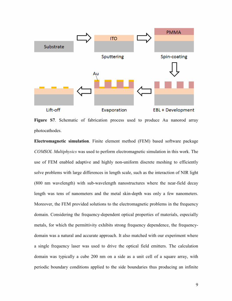
Figure S7. Schematic of fabrication process used to produce Au nanorod array
photocathodes.
Electromagnetic simulation. Finite element method (FEM) based software package
COMSOL Multiphysics was used to perform electromagnetic simulation in this work. The
use of FEM enabled adaptive and highly non-uniform discrete meshing to efficiently
solve problems with large differences in length scale, such as the interaction of NIR light
(800 nm wavelength) with sub-wavelength nanostructures where the near-field decay
length was tens of nanometers and the metal skin-depth was only a few nanometers.
Moreover, the FEM provided solutions to the electromagnetic problems in the frequency
domain. Considering the frequency-dependent optical properties of materials, especially
metals, for which the permittivity exhibits strong frequency dependence, the frequency-
domain was a natural and accurate approach. It also matched with our experiment where
a single frequency laser was used to drive the optical field emitters. The calculation
domain was typically a cube 200 nm on a side as a unit cell of a square array, with
periodic boundary conditions applied to the side boundaries thus producing an infinite

10
array of nanorods. Within each unit cell, a stacking structure of
vacuum/substrate/perfectly-matched-layer (PML) was modeled. Different substrate
materials were considered: Si, ITO, and ITO thin film on sapphire. The PML at the
bottom of the stack served as an absorbing layer for the incident electromagnetic wave. A
Au nanorod was placed at the vacuum/substrate interface. The nanorod had a rectangular
transverse cross section and two hemispherical end-caps. Sharp edges at the vacuum side
were rounded with a 3 nm curvature to avoid singularities in the calculation as well as to
better mimic the fabricated structure. The nanorod length, width, and thickness were
varied. A thin Ti layer was added between the nanorod and the substrate to model the
adhesion layer. The Ti layer thickness was 3 nm unless otherwise specified. The light
source was incident normal to the substrate from the top boundary where a port boundary
condition was applied. Testing of the boundary conditions showed very little
backscattered light was reflected by the port boundary condition and should have
negligible effect on the simulation results. The light was linearly polarized with the
polarization direction varied in the simulation. Boundaries with periodic condition were
identically meshed with triangular elements with a dimension smaller than one tenth of
the boundary dimension. The PML consisted of an adaptive mesh to reduce computation
complexity. Other objects within the calculation domain were adaptively meshed with
free tetrahedral elements of which the sizes were kept small enough so that each edge of
the object contained at least ten elements. The meshing was even finer at the edge
curvature and the adhesion layer when present. For optical properties of materials, the
dielectric constants of metals were taken from Johnson & Christy;7 the dielectric

11
constants of insulators were taken from Palik;8 and the dielectric constant of ITO was
taken from SOPRA N&K database.9
The nanorod and conducting substrate were treated as perfect conductors for electrostatic
simulations to model the DC response.
Electron emission simulations. For the simulation of emission process from the Au
nanorods, two problems are treated and solved synergistically. First, the FEM simulation
results from COMSOL are used to evaluate the normal electric field at the nanorod
surface. The Fowler-Nordheim model (equation S1) is then used to obtain the emission
current (J) at the surface.
J =e3 E
2
16π 2hWt2 (y)
e−
4 2me v(y)W 3/2
3he E (S1)
Here, e is the charge of the electron, me is the mass of the electron, W is the metal work-
function, E is the magnitude of the electric field (static and optical) and y, ν(y) and t(y)
are given in equations S2-4.
y =1−e3 E
4πε0
(S2)
t(y)=2π
4(
6447
2097152y5−
1305
262144y4+
15
2048y3−
1
256y2−
1
8y+1) (S3)
v(y)=3 2π
8(−
1995
262144y5−
141
8192y4−
13
256y2+ y) (S4)
The simulated emission current was found to best agree with the experimentally observed
charge-yield when the work-function of Au was set to 4.9 eV. Because of the
discretization in time and space the emitted charge in a time step from a surface element
may be less than the unit charge (e). Therefore, the obtained charge profile represents a

12
probability distribution for the position and momentum of the emitted electrons. Second,
the emitted electrons should be accelerated inside the electromagnetic fields. We
developed a fast search algorithm to find the four closest discretization nodes to the
charge position. Linear interpolation between the field values at these nodes returns the
electromagnetic fields at the charge point. To consider the space-charge effect on the
bunch variations, point-to-point approximation is used. For modeling the recombination
with the substrate or emitter surface, the charge points are reflected with a probability of
30% after they hit the surfaces.
Scanning electron microscopy. SEM images were acquired via an FEI Helios Dual
Beam SEM-FIB tool using a high-resolution magnetic immersion lens allowing sub-nm
resolution. Typical electron beam energy used was 5 or 10 keV and working distance was
about 4 mm.
UV-Vis spectroscopy. UV-Vis spectra of the samples were recorded by Cary 500i UV-
Vis-NIR spectrophotometer. A Harrick Scientific Corporation DPS-R4V depolarizer was
always attached before the detector to remove the effect of polarization on detected signal
level. For polarization-dependent measurement, a Harrick Scientific Corporation PGT-
S1V Glan-Taylor polarizer was attached after the light source to introduce linear
polarization with a tunable polarization angle. Samples were mounted upon a holder with
a 1 mm circular aperture. Nanorod arrays were aligned to the center of the aperture under
an optical microscope. The range of scan was set to 400 nm – 1200 nm. Scan rate was
200 nm/min, data interval 1 nm, and average time for each data point was 0.3 s.

13
Figure S8. Schematic representation of the photocathode testing setup. A Ti:Sapphire
laser outputting linearly polarized, 35 fs pulses of transform limited 800 nm central
wavelength light, was focused to a spot size of 90 µm (FWHM) at the Au nanorod array
photocathode. The photocathode was mounted on a manual XYZ translation stage within
a high-vacuum chamber at a pressure of ~ 1 × 10⁻⁸
mbar. The emission current was
measured at the cathode using a Keithley 6485 picoammeter, and also at the anode using
a Keithley 247 source-measurement unit.

14
Figure S9. Simulated static-field distribution for a cross-section through the Au nanorod
photocathode, and ring-anode. Materials of different parts are labeled. The cathode
substrate (ITO) is grounded and the anode (Al) is biased at 1000 V. The color scale
stands for electric field strength and the black arrows indicate the direction of local
electric field.

15
Figure S10. Plot of the effective area of emission at the nanorod array photocathode vs.
the natural log of the peak intensity of the laser. The straight line represents the area of
the laser spot on the photocathode having a threshold optical field of 0.26 GVm-1
. Square
data points represent the area calculated from equation (1) in the main text using the
values of slope obtained from figure 2 (b).

16
Figure S11. Plot of electron emission current vs. time for an array of Au nanorods
prepared without a Ti layer, similar to that shown in figure 1 (b) (axial pitch 200 nm,
radial pitch 100 nm). Average emission current is 2.7 nA (standard deviation 30 pA) for
a pulse-energy of 120 nJ and static bias of 1 kV.
The DC extracting field can also be enhanced at the nanorod end caps by the lightening-
rod effect. Consequently, we performed electrostatic simulations of the Au nanorod array,
assuming Au and ITO as perfect conductors and an anode bias of 1 kV with respect to the
grounded ITO surface (Figure S9). The static field distribution is plotted on a vertical
cross section across a nanorod in Figure S12, where the color scale represents static field
strength and the red arrows indicate the direction of local electric field. The static field-

17
enhancement factor is ~5 at the upper corners of the nanorod end caps. This results in an
enhanced static field of ~5 MV/m, which is more than two orders of magnitude lower
than the peak-field of the optical pulse. Thus, we conclude that electron emission was
induced by the optical field, at which point the electrons propagate in the static field to
the anode for collection. This static field distribution also suggests the extracting field is
more likely to pick up electrons emitter at the upper corners of the nanorods.
Figure S12. Simulated electrostatic field distribution. A vertical cross section across the
nanorod is shown. Pre-enhanced electric field strength is assumed to be 1 MV/m. Red
arrows indicate the direction of local electric field. The field-enhancement factor is ~5 at
the upper corners of the nanorod end caps.
Surface plasmon is known to have a finite lifetime in femtosecond scale. Therefore, the
actual time duration of optical field emission is longer than the optical pulse length. The

18
nanorod frequency-domain response, namely the field-enhancement spectrum, can be
treated as a band pass filter of the incoming optical pulse spectrum. Thus, the filtered
pulse spectrum has a narrower bandwidth and hence a prolonged temporal duration. We
studied this temporal response of LSPR by using the simulated field-enhancement spectra
and the spectrum of a 35 fs Fourier transform limited pulse with 38 nm FWHM. The
results of Au nanorod with and without a Ti adhesion layer are shown in Figure S13. In
Figure S13 (a), the pulse (field) spectrum, LSPR field-enhancement spectrum of Au
nanorod without a Ti layer, and the filtered pulse spectrum are illustrated. With this
spectral information, the temporal response of the optical pulse and plasmon pulse are
illustrated in Figure S13 (b). LSPR prolongs the pulse duration by 1.22 fs. The same
figures for Au nanorod with a Ti layer are shown in Figure S13 (c, d). LSPR prolongs the
pulse duration by 0.42 fs. These results are consistent with the fact that Ti adhesion layer
induces damping of LSPR and leads to shorter plasmon lifetime.

19
Figure S13. Spectral filtering and pulse elongation by LSPR. (a) Spectra of optical pulse
(blue), field-enhancement by Au nanorod without a Ti layer (red), and filtered pulse
(black). Optical pulse spectrum is the intensity spectrum of electric field. Field spectrum
is taken from simulation results (Figure 1(c)). Filtered pulse spectrum is calculated by
multiplying the above two spectra. (b) Optical and plasmon pulses calculated from (a).
(c), (d) The same plots as (a) (b), but for Au nanorod with a Ti layer.
References
(1) Knight, M. W.; Wu, Y.; Lassiter, J. B.; Nordlander, P.; Halas, N. J. Substrates Matter: Influence of
an Adjacent Dielectric on an Individual Plasmonic Nanoparticle. Nano Lett. 2009, 9, 2188–2192.

20
(2) Wu, Y.; Nordlander, P. Finite-Difference Time-Domain Modeling of the Optical Properties of
Nanoparticles near Dielectric Substrates. J. Phys. Chem. C 2010, 114, 7302–7307.
(3) Schweikhard, V.; Grubisic, A.; Baker, T. A.; Thomann, I.; Nesbitt, D. J. Polarization-Dependent
Scanning Photoionization Microscopy: Ultrafast Plasmon-Mediated Electron Ejection Dynamics in
Single Au Nanorods. ACS Nano 2011, 5, 3724–3735.
(4) Zhang, S.; Bao, K.; Halas, N. J.; Xu, H.; Nordlander, P. Substrate-Induced Fano Resonances of a
Plasmonic Nanocube: A Route to Increased-Sensitivity Localized Surface Plasmon Resonance
Sensors Revealed. Nano Lett. 2011, 11, 1657–1663.
(5) Hutter, T.; Elliott, S. R.; Mahajan, S. Interaction of Metallic Nanoparticles with Dielectric
Substrates: Effect of Optical Constants. Nanotechnology 2013, 24, 035201.
(6) Habteyes, T. G.; Dhuey, S.; Wood, E.; Gargas, D.; Cabrini, S.; Schuck, P. J.; Alivisatos, A. P.;
Leone, S. R. Plasmon Damping and Molecular Linker as a Nondamping Alternative. ACS Nano
2012, 6, 5702–5709.
(7) Johnson, P. B.; Christy, R. W. Optical Constants of the Noble Metals. Phys. Rev. B 1972, 6, 4370–
4379.
(8) Handbook of Optical Constants of Solids; Palik, E. D., Ed.; Academic Press: New York, 1985.
(9) SOPRA N&K Database http://www.sspectra.com/sopra.html.