High Temperature Annealing of Dislocations in ...cdn.intechweb.org/pdfs/28490.pdf · High...
18
16 High Temperature Annealing of Dislocations in Multicrystalline Silicon for Solar Cells Gaute Stokkan, Christoffer Rosario, Marianne Berg and Otto Lohne Norwegian University of Science and Technology (NTNU) Department of Materials Science and Engineering Norway 1. Introduction Dislocation clusters have been shown to constitute the main efficiency reducing factor for multicrystalline silicon solar cells (Sopori et al. 2005). Multicrystalline silicon is made under less ideal conditions compared to monocrystalline silicon, in the sense that thermal fields and the lack of seeding create material with increased density of crystal defects, but also since the direct contact between crystal/melt and crucible/coating provides a rapid channel for impurity contamination. These two factors make multicrystalline silicon inferior compared to monocrystalline silicon in terms of solar cell efficiency (Green et al. 2009). It has been shown by Kveder et al. (Kveder et al. 2001) that the interaction between dislocation levels and impurity levels in the band gap may provide very efficient recombination channels, thus enhancing the efficiency reduction both of the dislocations and the impurities. Furthermore it has been shown that gettering of impurities is far less efficient in regions of high dislocation density (Bentzen et al. 2006). Measures to reduce dislocation density in multicrystalline silicon is therefore of high interest. Interesting methods have been proposed to create more ideal conditions during solidification, such as seeding (Stoddard et al. 2008) and control of the nucleation conditions (Fujiwara et al. 2006); these conditions have also been shown to influence dislocation density (Stokkan 2010; Usami et al. 2010). It appears however very difficult to avoid or restrict the generation of dislocation clusters during solidification. Models have been proposed to explain the observed dislocation patterns from grain boundary sources (Ryningen et al. 2008; Takahashi et al. 2010; Usami et al. 2010). Therefore the possibility of improving dislocated structures by the process of recovery (Cahn et al. 1996) which has been shown to be very efficient for other materials such as aluminium and iron, may be investigated. Investigations by Patel on recovery in bent monocrystalline silicon rods indicated that a prolonged annealing times of 48 hours was necessary to achieve noticeable recovery at a temperature of 1300°C(Patel 1958). In contrast to this observation, more recent experiments performed on String Ribbon multicrystalline silicon indicated that it was possible to significantly reduce the dislocation density by a high temperature annealing step of the wafer (Hartman et al. 2008; Bertoni et al. 2010). These results were compared to models proposed by Kuhlmann (Kuhlmann 1951) and Nes (Nes 1995) and suggested to be explained by pairwise annihilation of dislocations. www.intechopen.com
Transcript of High Temperature Annealing of Dislocations in ...cdn.intechweb.org/pdfs/28490.pdf · High...
16
High Temperature Annealing of Dislocations in Multicrystalline Silicon for Solar Cells
Gaute Stokkan, Christoffer Rosario, Marianne Berg and Otto Lohne Norwegian University of Science and Technology (NTNU)
Department of Materials Science and Engineering Norway
1. Introduction
Dislocation clusters have been shown to constitute the main efficiency reducing factor for multicrystalline silicon solar cells (Sopori et al. 2005). Multicrystalline silicon is made under less ideal conditions compared to monocrystalline silicon, in the sense that thermal fields and the lack of seeding create material with increased density of crystal defects, but also since the direct contact between crystal/melt and crucible/coating provides a rapid channel for impurity contamination. These two factors make multicrystalline silicon inferior compared to monocrystalline silicon in terms of solar cell efficiency (Green et al. 2009). It has been shown by Kveder et al. (Kveder et al. 2001) that the interaction between dislocation levels and impurity levels in the band gap may provide very efficient recombination channels, thus enhancing the efficiency reduction both of the dislocations and the impurities. Furthermore it has been shown that gettering of impurities is far less efficient in regions of high dislocation density (Bentzen et al. 2006).
Measures to reduce dislocation density in multicrystalline silicon is therefore of high interest. Interesting methods have been proposed to create more ideal conditions during solidification, such as seeding (Stoddard et al. 2008) and control of the nucleation conditions (Fujiwara et al. 2006); these conditions have also been shown to influence dislocation density (Stokkan 2010; Usami et al. 2010).
It appears however very difficult to avoid or restrict the generation of dislocation clusters during solidification. Models have been proposed to explain the observed dislocation patterns from grain boundary sources (Ryningen et al. 2008; Takahashi et al. 2010; Usami et al. 2010). Therefore the possibility of improving dislocated structures by the process of recovery (Cahn et al. 1996) which has been shown to be very efficient for other materials such as aluminium and iron, may be investigated. Investigations by Patel on recovery in bent monocrystalline silicon rods indicated that a prolonged annealing times of 48 hours was necessary to achieve noticeable recovery at a temperature of 1300°C(Patel 1958). In contrast to this observation, more recent experiments performed on String Ribbon multicrystalline silicon indicated that it was possible to significantly reduce the dislocation density by a high temperature annealing step of the wafer (Hartman et al. 2008; Bertoni et al. 2010). These results were compared to models proposed by Kuhlmann (Kuhlmann 1951) and Nes (Nes 1995) and suggested to be explained by pairwise annihilation of dislocations.
www.intechopen.com
Solar Power
294
Further work by the same group indicated that residual or applied stress was a key factor for achieving the reported reduction in dislocation density (Bertoni et al. 2011).
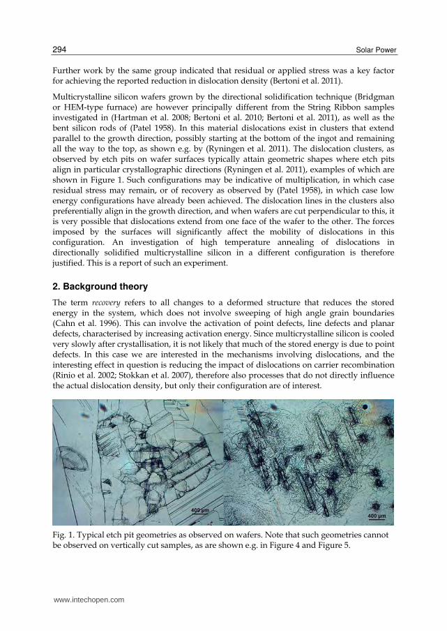
Multicrystalline silicon wafers grown by the directional solidification technique (Bridgman or HEM-type furnace) are however principally different from the String Ribbon samples investigated in (Hartman et al. 2008; Bertoni et al. 2010; Bertoni et al. 2011), as well as the bent silicon rods of (Patel 1958). In this material dislocations exist in clusters that extend parallel to the growth direction, possibly starting at the bottom of the ingot and remaining all the way to the top, as shown e.g. by (Ryningen et al. 2011). The dislocation clusters, as observed by etch pits on wafer surfaces typically attain geometric shapes where etch pits align in particular crystallographic directions (Ryningen et al. 2011), examples of which are shown in Figure 1. Such configurations may be indicative of multiplication, in which case residual stress may remain, or of recovery as observed by (Patel 1958), in which case low energy configurations have already been achieved. The dislocation lines in the clusters also preferentially align in the growth direction, and when wafers are cut perpendicular to this, it is very possible that dislocations extend from one face of the wafer to the other. The forces imposed by the surfaces will significantly affect the mobility of dislocations in this configuration. An investigation of high temperature annealing of dislocations in directionally solidified multicrystalline silicon in a different configuration is therefore justified. This is a report of such an experiment.
2. Background theory
The term recovery refers to all changes to a deformed structure that reduces the stored energy in the system, which does not involve sweeping of high angle grain boundaries (Cahn et al. 1996). This can involve the activation of point defects, line defects and planar defects, characterised by increasing activation energy. Since multicrystalline silicon is cooled very slowly after crystallisation, it is not likely that much of the stored energy is due to point defects. In this case we are interested in the mechanisms involving dislocations, and the interesting effect in question is reducing the impact of dislocations on carrier recombination (Rinio et al. 2002; Stokkan et al. 2007), therefore also processes that do not directly influence the actual dislocation density, but only their configuration are of interest.
Fig. 1. Typical etch pit geometries as observed on wafers. Note that such geometries cannot be observed on vertically cut samples, as are shown e.g. in Figure 4 and Figure 5.
www.intechopen.com
High Temperature Annealing of Dislocations in Multicrystalline Silicon for Solar Cells
295
The recovery mechanisms which may be in effect to reduce dislocation density or influence the recombination properties are: Elimination of stable dislocation dipoles (parallel, opposite dislocations with a small spatial separation), pairwise annihilation of dislocations of opposite sign, also called network growth, rearrangement of dislocations into stable configurations and increase in subgrain size.
Dislocation dipoles are created by interaction of gliding dislocations with either other dislocations or other obstacles (Nabarro 1987). They are therefore likely to be present in areas of high dislocation density and little symmetry in the dislocation arrangements, i.e. dislocation tangles. They are stable at the temperature they are created, but activation of other mechanisms such as climb and cross slip at higher temperature will allow the reduction of stored energy by their annihilation. Since the separation of dipoles is small, this is the process which is expected to be affecting the dislocation density first. Dipoles are observed in strained silicon (Jacques et al. 2000), but it is not clear to which extent such dipoles constitute a significant part of the total dislocation density, i.e. if their recovery will produce a noticeable reduction in dislocation density.
A general model for recovery by network growth in combination with growing subgrains
has been formulated by Nes (Nes 1995) where recovery is analysed in terms of rate
controlling mechanism: glide, cross slip, climb or solute drag. For dislocations to annihilate,
the opposite sign dislocations need to glide on parallel slip planes into a favourable position
and then migrate into the same slip plane, either by climb or cross slip. Silicon has a very
low stacking fault energy of ~50 mJ/mm2 which leads to the well known dissociation of
dislocations into Shockley partial dislocations. It has been a subject of debate whether this
dissociation appears during the glide process, or when the dislocations come to rest.
Investigations by Sato and Sumino (Sumino 1994) indicate that dislocations are dissociated
during glide. The resulting stacking fault makes both climb and cross slip difficult (Cahn et
al. 1996; Jacques et al. 2000) so we may well expect these mechanisms to be rate controlling
in a possible recovery process by network growth (pairwise annihilation). Cross slip is a
thermally activated process with activation energy 5.5 eV (Möller et al. 1979), and if there is
no supersaturation of vacancies or interstitials, climb is also a thermally activated process
with activation energy equal to that of self diffusion, i.e. 3.6 eV for temperature below 1250
K and 5 eV above 1300 K (Siethoff 1984). The different values are explained by different
diffusing species in the temperature ranges: Vacancies at lower and interstitials at higher
temperature. For the climb process it is the diffusion of these point defects from sources to
sinks that are rate limiting.
Arranging the dislocations into more energetically favourable positions may to some degree
happen only by gliding of a dislocation in one glide plane. To reduce stored energy further,
dislocations also need to move out of the primary slip plane by climb or cross slip.
It must also be mentioned that the degree to which recovery may happen by the processes
described above depends very much on the thermal history and the type of sources active in
the generation of dislocations. For instance a Frank-Read source will create dislocation loops
where the opposite sides of the loop have opposite sense but same Burgers’ vector; a
configuration well suited for pairwise annihilation and network growth. Other sources may
primarily generate dislocations of one sign only, like in the model of Kuhlmann (Kuhlmann
1951). An example of this may be a grain boundary source.
www.intechopen.com

Solar Power
296
In this context it should also be mentioned that directionally solidified multicrystalline silicon is routinely subjected to an annealing phase following the crystallisation and before cooling down to room temperature. This anneal is performed at a temperature higher than the brittle to ductile transition temperature, commonly between 1000 and 1200°C. It was historically introduced to reduce long range residual stresses which would result in the material cracking upon being subjected to mechanical impact (sawing) after cooling to room temperature (Hukin) and is appropriately termed stress relief. The equipment used today offers more ideal thermal conditions than the early equipment, and the need for stress relief may not be as high as it was.
Recent TEM investigations (Kivambe et al. 2011) on dislocation clusters which show the above mentioned alignment of etch pits along crystallographic directions have shown that the dislocations have an edge component, and that the alignment is perpendicular to the direction of the Burgers’ vector, i.e. the slip plane. This result indicates that the dislocations have aligned in order to reduce their total energy, i.e. some degree of recovery has already occurred during growth, and the dislocations have already attained low energy configurations, which may make further recovery difficult. This indicates that the residual stresses believed to be responsible for the dislocation density reduction reported in (Bertoni et al. 2011) may already have been relieved in directionally solidified multicrystalline silicon.
The above discussion indicates that recovery by the process of dipole annihilation and arranging into more stable configurations are likely to occur when silicon is annealed, depending on to which degree the already existing dislocation structures are already a result of recovery. The process of pairwise annihilation involves processes of higher activation energy and it is therefore more questionable if this recovery process will occur and at which rate it will be effective.
Another process that may change the configuration of dislocations is when they move under the influence of image forces (Hirth and Lothe 1992). Image forces are used to describe the forces between dislocations and crystal surfaces and interfaces. The simplest case is the interaction between a dislocation and a free surface. In this case the force can be modelled by extending the crystal lattice on the other side of the surface and placing a dislocation of opposite sign at the same distance from the surface. These dislocations attract each other, and the dislocation will be attracted by the surface. If the surface is not free, but rather an interface to a different medium, the properties will be changed accordingly. The governing parameter is the elastic modulus E; the smaller the difference in stiffness between the silicon and the other medium, the smaller is the attraction. If the other medium is stiffer than the silicon, the dislocation will be repulsed from the surface.
Image forces from the surface may influence the dislocation density near the sample surface during annealing if dislocations are attracted towards the surface, as shown in Figure 2. Depending on the dislocation distance from the surface, it may annihilate at the surface or change its direction to lower the total length and reduce its energy. Further into the sample the effect may not be so efficient, primarily since the attractive force is inversely proportional to the distance, but also because of screening by other dislocations. Since the dislocations annihilate at any point they meet the surface, they can in principle move towards the surface only by glide if the slip plane is favourably oriented. The high activation energy processes of climb and cross slip should therefore be of less importance than for pairwise annihilation discussed above.
www.intechopen.com

High Temperature Annealing of Dislocations in Multicrystalline Silicon for Solar Cells
297
A native oxide on the sample surface is only 1-2 nm thick (Zhang 2001) and will not influence the image forces very much. If a layer is deliberately added to the surface, like a diffusion barrier, or if a thermal oxide builds up on the surface during the process, the situation may be different.
Lastly the work of Siethoff et al. should be mentioned, who in a series of reports (Siethoff and Schroter 1978; Siethoff and Schroter 1983; Siethoff 1984; Siethoff et al. 1984; Siethoff et al. 1986) investigated the mechanisms of dynamic recovery. Dynamic recovery differs from the process studied here in that it describes reduction of stored energy during hot working (Cahn et al. 1996), i.e. under an applied stress. Nevertheless much information about the mechanisms for dislocation movement is gained from this work, as will be discussed later.
Fig. 2. Illustration of the effect of image forces on dislocations moving in a slip plane crossing the sample surface. a) Before annealing. b) After annealing. Dislocation 1 close to the surface has disappeared while dislocation 2 further away from the surface has changed direction to reduce its total energy.
3. Experimental work
Slices of approximately 2 mm thickness were cut from two different multicrystalline silicon ingots (A and B) produced in a pilot scale directional solidification furnace. In this type of furnace, crystal growth proceeds by heterogeneous nucleation at several points on the interface between the crucible lining and the melt, followed by dendritic growth in a supercooled part of the melt close to the crucible bottom. This growth is largely parallel to the crucible bottom, and directional solidification proceeds on top of this solidified layer. The size of the ingots produced in this particular furnace is 100-120 mm high and 250 mm in diameter. The slices were cut parallel to the growth direction to avoid the direct interaction between dislocations extending in the growth direction, and the surfaces. They were
Surface
Slip plane
Dislocation 1
Dislocation 2
a) b)
Dislocation 2
www.intechopen.com
Solar Power
298
subjected to a series of surface preparation techniques, measurements, high temperature treatment, followed by surface preparation and measurements again, all detailed in Table 1.
The sample was ground and polished as a prerequisite for the defect delineation by etching, but also as preparation for measurements of Carrier lifetime and substitutional carbon and interstitial oxygen. The lifetime was measured with Carrier Density Imaging (CDI) (Isenberg et al. 2003; Schubert et al. 2003). The surfaces were not passivated, so only relative differences in lifetime could be observed. However since the surfaces were polished, optical measurement problems (Schubert et al. 2007) could be avoided and high quality images were obtained. The interstitial oxygen and substitutional carbon level was measured with Fourier Transform Infrared Spectroscopy (FTIR).
Step Purpose Procedure
1 Sample surface preparation Plane grinding, grinding, mechanical polishing, chemical mechanical polishing
2 Characterisation CDI, FTIR
3 Defect delineation Sopori etch 30 s
4 Characterisation PVScan, dislocation counting
5 Removal of defect delineation Polishing, chemical mechanical polishing
6 Thermal ramp up 20°C/min (A) and 7°C/min (B)
7 Anneal 4 h at 1350 °C
8 Thermal cool down 7°C/min
9 Removal of surface deposit Grinding and/or polishing, chemical mechanical polishing
10 Characterisation CDI, FTIR
11 Defect delineation Sopori etch 30 s
12 Characterisation PVScan, dislocation counting
Table 1. Sequence of the experiments
Dislocations are delineated by the use of the Sopori etch, which creates large etch pits (~5
µm, round or elliptical depending on whether the dislocation line penetrates the surface
perpendicular or at an angle (Sopori 1984). This property can be used to substantiate the
hypothesis that dislocations lines primarily run in the direction parallel to the growth
direction, i.e. parallel to the sample surface here, since this should cause a higher occurrence
of elliptical etch pits compared to an etched wafer surface. PVScan is a tool designed to
provide a quantitative measurement of etch pit density on samples etched with this solution
(Sopori et al. 2000). The quantitative measurement of etch pit density is interpreted as
dislocation density. Dislocation density is however defined as total length of dislocation
lines inside a volume divided by the volume, and the justification of this interpretation
depends on the angle of the dislocation lines to the etched surface. Thus in this case the
measurement probably provides an underestimate. To achieve measurements of higher
spatial resolution and to be able to study the dislocation structures in detail, the entire
samples were photographed in an optical microscope with an automated xy-stage and
image capture control. By this method images of magnification 80x were obtained.
www.intechopen.com

High Temperature Annealing of Dislocations in Multicrystalline Silicon for Solar Cells
299
All traces of the defect delineation had to be removed from the sample before the thermal treatment; this was done by mechanical polishing followed by chemical mechanical polishing.
The thermal treatment was performed at atmospheric pressure in an alumina tube furnace flushed with high purity argon (5.0), the samples resting horizontally on an alumina boat supporting the long edges of the sample. Two different furnaces were used. The furnace used for sample A was expected to be heavily contaminated by Titanium, whereas the second, used for sample B was expected to provide a cleaner atmosphere. No external stress was applied to the samples during the heat treatment. After the heat treatment, the samples were covered by a thick film, apparently thicker for the side facing towards the support. This film was removed by polishing, and then the samples were subjected to the same sample preparation and characterisation as before.
4. Results
Figure 3 shows the dislocation density measured by PVScan before heat treatment as well as lifetime measured before heat treatment for sample A. It is seen that apart from the top region, low dislocation density and high lifetime corresponds well and vice versa. After heat treatment, however the lifetime is reduced below measurable levels.
Fig. 3. Dislocation density (a) and lifetime (b) measured before heat treatment of sample A. The poor sample preparation leads to higher apparent values than realistic in low dislocation density areas, however high dislocation density areas are clearly visible. The lifetime measurements were performed on an unpassivated sample, thus the lifetime is not a true bulk lifetime. The scaling is in mm , and the colour bars are in cm-2 and microseconds for a) and b) respectively.
www.intechopen.com
Solar Power
300
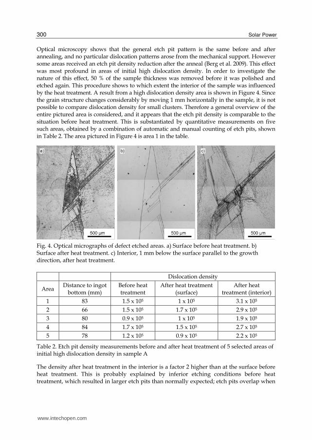
Optical microscopy shows that the general etch pit pattern is the same before and after annealing, and no particular dislocation patterns arose from the mechanical support. However some areas received an etch pit density reduction after the anneal (Berg et al. 2009). This effect was most profound in areas of initial high dislocation density. In order to investigate the nature of this effect, 50 % of the sample thickness was removed before it was polished and etched again. This procedure shows to which extent the interior of the sample was influenced by the heat treatment. A result from a high dislocation density area is shown in Figure 4. Since the grain structure changes considerably by moving 1 mm horizontally in the sample, it is not possible to compare dislocation density for small clusters. Therefore a general overview of the entire pictured area is considered, and it appears that the etch pit density is comparable to the situation before heat treatment. This is substantiated by quantitative measurements on five such areas, obtained by a combination of automatic and manual counting of etch pits, shown in Table 2. The area pictured in Figure 4 is area 1 in the table.
Fig. 4. Optical micrographs of defect etched areas. a) Surface before heat treatment. b) Surface after heat treatment. c) Interior, 1 mm below the surface parallel to the growth direction, after heat treatment.
Dislocation density
Area Distance to ingot
bottom (mm) Before heat treatment
After heat treatment (surface)
After heat treatment (interior)
1 83 1.5 x 10⁵ 1 x 10⁵ 3.1 x 10⁵
2 66 1.5 x 10⁵ 1.7 x 10⁵ 2.9 x 10⁵
3 80 0.9 x 10⁵ 1 x 10⁵ 1.9 x 10⁵
4 84 1.7 x 10⁵ 1.5 x 10⁵ 2.7 x 10⁵
5 78 1.2 x 10⁵ 0.9 x 10⁵ 2.2 x 10⁵
Table 2. Etch pit density measurements before and after heat treatment of 5 selected areas of initial high dislocation density in sample A
The density after heat treatment in the interior is a factor 2 higher than at the surface before heat treatment. This is probably explained by inferior etching conditions before heat treatment, which resulted in larger etch pits than normally expected; etch pits overlap when
www.intechopen.com

High Temperature Annealing of Dislocations in Multicrystalline Silicon for Solar Cells
301
the dislocation density becomes large and cannot be discriminated by the counting procedure, and these larger etch pits overlap at a lower dislocation density than normal. This may also explain the apparently slightly increasing etch pit density for two of the areas.
Even though these results show a clear etch pit density reduction close to the surface, but not in the interior, it became clear that the varying etching conditions made it difficult to quantify the changes accurately. The experiment was therefore repeated with sample B, this time in a different furnace. Quantitative results are shown in Table 3.
Dislocation density
Area Distance to ingot
bottom (mm) Before heat
treatment (cm-3) After heat
treatment (cm-3) Remaining amount of
etch pits (%)
1 96 2 x 10⁵ 1.9 x 10⁵ 95
2 82 4.6 x 10⁵ 4.5 x 10⁵ 97
3 56 6.1 x 10⁵ 5.6 x 10⁵ 91
4 96 2.6 x 10⁵ 2.4 x 10⁵ 90
5 82 1.4 x 10⁵ 0.7 x 10⁵ 54
6 56 7.7 x 10⁵ 4.7 x 10⁵ 61
Table 3. Etch pit density before and after high temperature treatment of sample B. Areas 1-3 are from the side facing downwards in the furnace whereas 4 - 6 face upwards.
It can be seen that the surface etch pit density is reduced similarly to sample A. It is also
seen that the side facing towards the centre of the furnace receives a higher reduction than
the side facing towards the support. The side with higher reduction in dislocation density
also had a thinner film. The film was chemically analysed by EDS, which showed peaks
corresponding to Silicon, Aluminium and Oxygen.
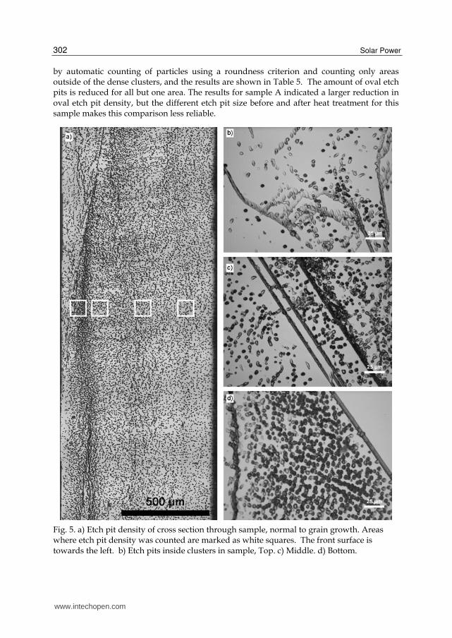
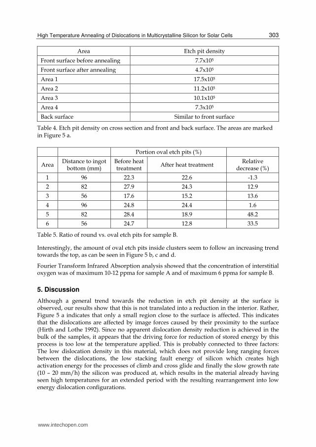
To investigate if an effect to the sample interior could be observed, a particular area showing initial high etch pit density both at the front and back surface was selected. This area was expected to consist of one large, relatively homogeneous dislocation cluster and was therefore ideal for comparisons of different faces. The sample was cut parallel to the growth direction so that the cut made a cross section through the cluster. The cross section was polished and etched and is shown in Figure 5 a. It shows a relatively homogeneous etch pit density, but a slight decrease in area of less than 50 µm from the edges (i.e. less than 50 µm depth) is observed. The etch pits were counted in four different areas, which are compared to the situation before and after heat treatment at the surface in Table 4.
The etch pit density in the interior is very similar to the density at the surfaces before heat
treatment. This shows that we do not see any recovery effect of dislocations in the sample
interior. The observed variations are probably caused by local variations in the crystal not
related to the heat treatment.
Finally the ratio of round versus oval etch pits was investigated to study the angle at which the dislocations penetrate the surface. This was done in order to identify an effect from image forces, as dislocations that have aligned orthogonal to the surface (such as dislocation 2 in Figure 2) will change the etch pit shape from round to oval. The investigation was done
www.intechopen.com
Solar Power
302
by automatic counting of particles using a roundness criterion and counting only areas outside of the dense clusters, and the results are shown in Table 5. The amount of oval etch pits is reduced for all but one area. The results for sample A indicated a larger reduction in oval etch pit density, but the different etch pit size before and after heat treatment for this sample makes this comparison less reliable.
Fig. 5. a) Etch pit density of cross section through sample, normal to grain growth. Areas where etch pit density was counted are marked as white squares. The front surface is towards the left. b) Etch pits inside clusters in sample, Top. c) Middle. d) Bottom.
www.intechopen.com
High Temperature Annealing of Dislocations in Multicrystalline Silicon for Solar Cells
303
Area Etch pit density
Front surface before annealing 7.7x10⁵
Front surface after annealing 4.7x10⁵
Area 1 17.5x10⁵
Area 2 11.2x10⁵
Area 3 10.1x10⁵
Area 4 7.3x10⁵
Back surface Similar to front surface
Table 4. Etch pit density on cross section and front and back surface. The areas are marked in Figure 5 a.
Portion oval etch pits (%)
Area Distance to ingot
bottom (mm)Before heat treatment
After heat treatment Relative
decrease (%)
1 96 22.3 22.6 -1.3
2 82 27.9 24.3 12.9
3 56 17.6 15.2 13.6
4 96 24.8 24.4 1.6
5 82 28.4 18.9 48.2
6 56 24.7 12.8 33.5
Table 5. Ratio of round vs. oval etch pits for sample B.
Interestingly, the amount of oval etch pits inside clusters seem to follow an increasing trend towards the top, as can be seen in Figure 5 b, c and d.
Fourier Transform Infrared Absorption analysis showed that the concentration of interstitial oxygen was of maximum 10-12 ppma for sample A and of maximum 6 ppma for sample B.
5. Discussion
Although a general trend towards the reduction in etch pit density at the surface is observed, our results show that this is not translated into a reduction in the interior. Rather, Figure 5 a indicates that only a small region close to the surface is affected. This indicates that the dislocations are affected by image forces caused by their proximity to the surface (Hirth and Lothe 1992). Since no apparent dislocation density reduction is achieved in the bulk of the samples, it appears that the driving force for reduction of stored energy by this process is too low at the temperature applied. This is probably connected to three factors: The low dislocation density in this material, which does not provide long ranging forces between the dislocations, the low stacking fault energy of silicon which creates high activation energy for the processes of climb and cross glide and finally the slow growth rate (10 – 20 mm/h) the silicon was produced at, which results in the material already having seen high temperatures for an extended period with the resulting rearrangement into low energy dislocation configurations.
www.intechopen.com
Solar Power
304
The multicrystalline silicon investigated in this study has a relatively low dislocation density ranging from ~104 cm-3 in good areas to 108 cm-3 in the very dense clusters, whereas the dislocation density after cold working of metals is in the range 1010 to 1012 cm-3 (Nes 1995; Cahn et al. 1996). Since the force Fr between parallel dislocation segments is inversely proportional to their distance, e.g. given by
2
2r
GbF
r (1)
for a screw dislocation, where G is the shear modulus, b is the magnitude of the Burgers’ vector and r is the distance between the segments, the driving force for network growth is expected to be much lower in the case of multicrystalline silicon. However, considering the observation in Figure 5 a) that image forces may operate down to a depth of ~50 µm, the forces in high dislocation areas (>106 cm-3) should be adequate to generate motion in the slip planes. But although dislocations are highly mobile in the slip planes at the temperature applied in this experiment, not being restricted by the lattice resistance (Argon 2007), climb and cross glide are essential for network growth of dislocations and may be expected to be rate limiting.
Cross slip has indeed been observed in silicon at lower temperature than applied in this experiment by several authors (Möller et al. 1979; Jacques et al. 2000). Jacques et al. (Jacques et al. 2000) subjected silicon to stresses in the range of 10 MPa at temperatures between 975 and 1075 K. The force on the dislocations, calculated by
,rF b (2)
where τ is the applied stress, is Fr = 0.00384 Nm-1 for a force of 10 MPa and Burgers’ vector of 0.384 nm, whereas the attractive force between parallel, opposite screw dislocations calculated from equation 1 is Fr = 0.0015 Nm-1 for a dislocation density of ρ = 106 cm-2, using the elastic constants of (Burenkov and Nikanorov 1974) at 973 K. These numbers are of similar magnitude, therefore cross slip could be expected to occur, in spite of the high activation energy. Cross slip was also observed by Möller et al. (Möller et al. 1979) without applied load at a temperature of T>1170 K, the driving force in this case being image force from the sample surface.
Siethoff and Schröter (Schröter and Siethoff 1984; Siethoff 1984) argue that during dynamic recovery, stage III of the stress-strain curve, which corresponds to the first recovery stage at lower strains, the rate controlling mechanism is that of diffusion of vacancies connected to a climb process. The diffusion D constant is given by
0
B
U
k TD D e . (3)
In silicon, analysis of the self diffusion parameters D0 and U point to two different diffusion mechanisms being operative at different temperature: a vacancy mechanism below 1250°C and an interstitial mechanism above 1300°C (Siethoff 1984). For the low temperature regime D0 = 0.35 cm2s-1 and U = 3.9; for high temperature D0 = 1460 cm2s-1 and U = 5 eV . Using the latter, a diffusion constant D = 4.3*10-13 cm2/s is calculated (it can be noted that the parameters calculated for the vacancy mechanism, if used in the calculation at 1350°C will give a value of D = 2.9*10-13, not very different from the interstitial mechanism). The expression
www.intechopen.com
High Temperature Annealing of Dislocations in Multicrystalline Silicon for Solar Cells
305
dL Dt (4)
for diffusion length gives a value Ld = 0.8 µm for 4 hours annealing at 1350°C. The sources
and sinks for point defects are grain boundaries and other dislocations which are a distance
from 10 µm up to several mm away from the dislocation. This shows that diffusion of point
defects to support climb may very well be a rate limiting process for this defect geometry,
impeding the recovery by network growth.
It should be noted that in regions of very high dislocation density (~108 cm-3), forces
between dislocations will increase and distance between sources and sinks of point defects
will decrease. Changes in such areas are not detectable by this experimental technique
because of the overlapping etch pits. We may therefore not rule out the possibility of
reduction of dislocation density in such regions by the observations and discussion above.
Interestingly, another element with low stacking fault energy, copper, shows very little
response to recovery (Cahn et al. 1996; Martin et al. 1997) , as appears to be the case also for
silicon in this experiment.
Migration towards the surfaces under the influence of image forces is not dependent on
these rate limiting processes to the same extent if slip planes are favourably oriented, and it
is therefore not surprising to see that this occurs, an effect observed both by the reduction in
dislocation density in the proximity of the surface and in the transformation of oval etch pits
to round. Different orientation of slip planes towards the surface may be a factor influencing
the varying degree of reduction experienced in different areas.
For sample B there is a correlation between the amount of reduction of dislocation density,
the change from oval to round etch pits and the amount of oval vs. round etch pits in
clusters as a function of distance from the ingot bottom. This can be seen by comparing the
data in Table 3, Table 5 and Figure 5. This again points to the image forces as the main
driving force for dislocation density reduction near the surface.
Another factor influencing the efficacy of the surface in reducing dislocation density is the
formation of a surface film during the heat treatment. After this film forms, the surface is no
longer to be regarded as a free surface; the film may reduce the attraction to the surface, the
governing factors being the elastic modulus and the thickness. For sample B a possible
correlation was observed between the increased thickness of the layer and the reduced
attraction of the surface for the two different sides, which can be explained by this influence.
Another possible explanation is that the samples had to be polished different periods of time
to remove the surface film, and this may also have influenced how much of the sample was
polished away.
We do not find a simple correlation between the reduction in dislocation density and the
oxygen values. For sample A a higher degree of reduction was experienced towards the top
of the sample, whereas for sample B a trend towards a more efficient reduction towards the
bottom is observed. The solubility of oxygen at 1350°C is 35 ppma (Pajot 1999), higher by a
factor of 3 than the highest measured value in the samples studied here. Any oxygen
precipitates on the dislocations should therefore be dissolved and not influence the mobility
of the dislocations during the heat treatment.
www.intechopen.com

Solar Power
306
6. Conclusion
We have shown that by performing an anneal of 4 h at 1350°C on bulk silicon samples, a quantifiable reduction in etch pit density is observed. This reduction is however only visible near the sample surface. A region in the range of less than 50 µm from the surface seems to be affected. No true bulk recovery is observed; the effect is attributed to image forces from the surface. The observations correspond well to theoretical predictions based on forces between dislocations at the given dislocation densities and restrictions to dislocation mobility by the process of climb and possibly also cross slip. These restrictions are caused by the low stacking fault energy of silicon which through the dissociation of dislocations into Shockley partials creates high activation energies for these processes.
It is very likely that the dislocations have already undergone recovery during the cooling of the ingot in the production process, at even higher temperatures than applied in this experiment. Thus the potential for lowering the total energy by dislocation migration is low in this material.
Since the image forces appear to be effective down to a thickness comparable to current wafer thickness, one can imagine a process where this force is utilised to reduce dislocation density of wafers. It is then important to take into account the orientation of the dislocation lines compared to the surface. Since dislocation clusters seem to follow the crystalline structure of directionally grown multicrystalline silicon, one may suggest that wafers cut parallel to the growth direction may be more receptive to such treatment than the current method of cutting parallel to the growth interface. This suggestion of course does not take into account other benefits of the currently preferred cutting direction. It should also be mentioned that if a diffusion barrier is applied to the surface to prevent contamination, the elastic modulus of this material may influence the magnitude of the image force.
7. Acknowledgements
This work was carried out in the projects “Crystalline Silicon Solar Cells – Cost Reduction” and “Defect Engineering in Crystalline Silicon Solar Cells” sponsored by The Norwegian Research Council, Elkem Solar and REC. Maulid Kivambe, Torunn Ervik, Birgit Ryningen and Ketill O. Pedersen are acknowledged for helpful discussions, and Eivind Øvrelid and Øyvind Mjøs for growing the crystals that were studied.
8. References
Argon, A. (2007). Strengthening Mechanisms in Crystal Plasticity. Oxford, Oxford University Press.
Bentzen, A., A. Holt, et al. (2006). "Gettering of transition metal impurities during phosphorous emitter diffusion in multicrystalline silicon solar cell processing." J. Appl. Phys. 99(9): 93509-93501.
Berg, M., G. Stokkan, et al. (2009). High temperature annealing of dislocations in silicon. Third International Workshop on Crystalline Silicon Solar Cells CSSC3, Trondheim.
Bertoni, M., C. Colin, et al. (2010). "Dislocation Engineering in Multicrystalline Silicon." Diffusion and Defect Data Part B (Solid State Phenomena) 156-8: 11-18.
Bertoni, M. I., D. M. Powell, et al. (2011). "Stress-enhanced dislocation density reduction in multicrystalline silicon." physica status solidi (RRL) – Rapid Research Letters 5(1): 28-30.
www.intechopen.com
High Temperature Annealing of Dislocations in Multicrystalline Silicon for Solar Cells
307
Burenkov, Y. A. and S. P. Nikanorov (1974). "Temperature dependence of the elastic constants of silicon." Soviet Physics - Solid State 16(5): 963-964.
Cahn, R. W., W. C. Robert, et al. (1996). Recovery and Recrystallization. Physical Metallurgy (Fourth Edition). Oxford, North-Holland: 2399-2500.
Fujiwara, K., W. Pan, et al. (2006). "Growth of structure-controlled polycrystalline silicon ingots for solar cells by casting." Acta Materialia 54(12): 3191-3197.
Green, M. A., K. Emery, et al. (2009). "Solar cell efficiency tables (version 33)." Progress in Photovoltaics: Research and Applications 17(1): 85-94.
Hartman, K., M. Bertoni, et al. (2008). "Dislocation density reduction in multicrystalline silicon solar cell material by high temperature annealing." Applied Physics Letters 93(12): 122108 (122103 pp.).
Hirth, J. P. and J. Lothe (1992). Theory of dislocations. Malabar, Fla., Krieger Publ. Co. Hukin, D. Personal communication. Isenberg, J., S. Riepe, et al. (2003). "Imaging method for laterally resolved measurement of
minority carrier densities and lifetimes: Measurement principle and first applications." J. Appl. Phys. 93(7): 4268-4275.
Jacques, A., F. Vallino, et al. (2000). "Dislocation multiplication in silicon at the onset of plasticity observed by in situ synchrotron X-ray topography." J. Phys., Condens. Matter. (UK) 12: 10045-10058.
Kivambe, M., T. Ervik, et al. (2011). "The microstructure of dislocation clusters in industrial directionally solidified multicrystalline silicon." To be published.
Kuhlmann, D. (1951). "On the Theory of Plastic Deformation." Proceedings of the Physical Society. Section A 64(2): 140.
Kveder, V., M. Kittler, et al. (2001). "Recombination activity of contaminated dislocations in silicon: A model describing electron-beam-induced current contrast behavior." Physical Review B (Condensed Matter and Materials Physics) 63(11): 115208-115201.
Martin, J. W., R. D. Doherty, et al. (1997). Stability of microstructure in metallic systems. Cambridge, Cambridge University Press.
Möller, H. J., H. Ewaldt, et al. (1979). "Cross slip of single dissociated screw dislocations in silicon and germanium." Physica Status Solidi A 55(2): 469-478.
Nabarro, F. R. N. (1987). Theory of crystal dislocations. New York, Dover. Nes, E. (1995). "Recovery revisited." Acta Metallurgica et Materialia 43(6): 2189-2207. Pajot, B. (1999). Solubility of O in c-Si. Properties of crystalline silicon. R. Hull. London,
INSPEC, the Institution of Electrical Engineers: 488-491. Patel, J. R. (1958). "Arrangements of dislocations in plastically bent silicon crystals." Journal
of Applied Physics 29(2): 170-176. Rinio, M., S. Peters, et al. (2002). "Measurements of the normalized recombination strength
of dislocations in multicrystalline silicon solar cells." Solid State Phenomena 82-84: 701-706.
Ryningen, B., G. Stokkan, et al. (2011). "Growth of dislocation clusters during directionally solidification of multicrystalline silicon ingots " To be published.
Ryningen, B., G. Stokkan, et al. (2008). Growth of Dislocation Clusters in Directionally Solidified Multicrystalline Silicon. 23rd European Photovoltaic Solar Energy Conference, Valencia, SPAIN, WIP - Munich.
www.intechopen.com

Solar Power
308
Schröter, W. and H. Siethoff (1984). "New phenomena in the plasticity of semiconductors and fcc metals at high temperatures. Part II: Analysis of experimental data." Zeitschrift für Metallkunde 75(7): 482-491.
Schubert, M., J. Isenberg, et al. (2003). "Spatially resolved lifetime imaging of silicon wafers by measurement of infrared emission." J. Appl. Phys. 94(6): 4139-4143.
Schubert, M. C., S. Pingel, et al. (2007). "Quantitative carrier lifetime images optically measured on rough silicon wafers." Journal of Applied Physics 101(12).
Siethoff, H. (1984). "New phenomena in the plasticity of semiconductors and FCC metals at high temperatures. I. Theoretical models." Zeitschrift für Metallkunde 75(7): 475-481.
Siethoff, H., K. Ahlborn, et al. (1984). "Two independent mechanisms of dynamical recovery in the high-temperature deformation of silicon and germanium." Philosophical Magazine A (Physics of Condensed Matter, Defects and Mechanical Properties) 50(1): 1-6.
Siethoff, H., H. G. Brion, et al. (1986). "Dynamical recovery of 111 germanium." Physica Status Solidi A 97(1): 153-162.
Siethoff, H. and W. Schroter (1978). "Dynamical recovery and self-diffusion in silicon." Philosophical Magazine A (Physics of Condensed Matter, Defects and Mechanical Properties) 37(6): 711-718.
Siethoff, H. and W. Schroter (1983). "Work hardening and dynamical recovery in silicon and germanium at high temperatures and comparison with FCC metals." Scripta Metallurgica 17(3): 393-398.
Sopori, B., C. Li, et al. (2005). Efficiency limitations of multicrystalline silicon solar cells due to defect clusters, Warrendale, PA, USA, Materials Research Society.
Sopori, B., C. Wei, et al. (2000). "High-speed mapping of grown-in defects and their influence in large-area silicon photovoltaics." Journal of Crystal Growth 210: 346-350.
Sopori, B. L. (1984). "A new defect etch for polycrystalline silicon." Journal of the Electrochemical Society 131(3): 667-672.
Stoddard, N., W. Bei, et al. (2008). Casting single crystal silicon: novel defect profiles from BP solar's mono2 wafers, Erice, Italy, Trans Tech Publications Ltd.
Stokkan, G. (2010). "Relationship between dislocation density and nucleation of multicrystalline silicon." Acta Materialia 58(9): 3223-3229.
Stokkan, G., S. Riepe, et al. (2007). "Spatially resolved modeling of the combined effect of dislocations and grain boundaries on minority carrier lifetime." J. Appl. Phys.
Sumino, K. (1994). Mechanical behaviour of semiconductors. Handbook on Semiconductors, Materials, properties and preparation. S. Mahajan. Amsterdam, North-Holland. Vol. 3: 76-181.
Takahashi, I., N. Usami, et al. (2010). "Generation mechanism of dislocations during directional solidification of multicrystalline silicon using artificially designed seed." Journal of Crystal Growth 312(7): 897-901.
Usami, N., R. Yokoyama, et al. (2010). "Relationship between grain boundary structures in Si multicrystals and generation of dislocations during crystal growth." Journal of Applied Physics 107(1): 013511 (013515 pp.).
Zhang, X. G. (2001). Electrochemistry of silicon and its oxide. New York, Kluwer Academic/Plenum Publishers.
www.intechopen.com

Solar PowerEdited by Prof. Radu Rugescu
ISBN 978-953-51-0014-0Hard cover, 378 pagesPublisher InTechPublished online 15, February, 2012Published in print edition February, 2012
InTech EuropeUniversity Campus STeP Ri Slavka Krautzeka 83/A 51000 Rijeka, Croatia Phone: +385 (51) 770 447 Fax: +385 (51) 686 166www.intechopen.com
InTech ChinaUnit 405, Office Block, Hotel Equatorial Shanghai No.65, Yan An Road (West), Shanghai, 200040, China
Phone: +86-21-62489820 Fax: +86-21-62489821
A wide variety of detail regarding genuine and proprietary research from distinguished authors is presented,ranging from new means of evaluation of the local solar irradiance to the manufacturing technology ofphotovoltaic cells. Also included is the topic of biotechnology based on solar energy and electricity generationonboard space vehicles in an optimised manner with possible transfer to the Earth. The graphical materialsupports the presentation, transforming the reading into a pleasant and instructive labor for any interestedspecialist or student.
How to referenceIn order to correctly reference this scholarly work, feel free to copy and paste the following:
Gaute Stokkan, Christoffer Rosario, Marianne Berg and Otto Lohne (2012). High Temperature Annealing ofDislocations in Multicrystalline Silicon for Solar Cells, Solar Power, Prof. Radu Rugescu (Ed.), ISBN: 978-953-51-0014-0, InTech, Available from: http://www.intechopen.com/books/solar-power/high-temperature-annealing-of-dislocations-in-multicrystalline-silicon-for-solar-cells

© 2012 The Author(s). Licensee IntechOpen. This is an open access articledistributed under the terms of the Creative Commons Attribution 3.0License, which permits unrestricted use, distribution, and reproduction inany medium, provided the original work is properly cited.