High-Speed Bus Architecture and Data Transmission Technology ...
29
Prepared by eSilicon Corporation, Copyright July 2001 High-Speed Bus Architecture and Data Transmission Technology Overview Xu Jiang
Transcript of High-Speed Bus Architecture and Data Transmission Technology ...

Prepared by eSilicon Corporation, Copyright July 2001
High-Speed Bus Architecture and
Data Transmission Technology Overview
Xu Jiang

High-Speed Bus Architecture and Data Transmission Technology Overview
Prepared by eSilicon Corporation, Copyright July 2001 Page 2 of 29
Introduction High speed and low power embedded processors are used frequently in today’s high performance networking and communication systems, digital consumer electronics, and office automation applications. It is extremely important for the equally fast I/O and multiprocessor busses to keep pace with them so as to enable an effective product solution. In addition, communication protocols for connecting systems and networks are advancing the pace of data transfers from the Ethernet standards of the past to the 10 Gigabit and OC-192 speeds of today. There are several emerging bus architectures, such as the InfiniBand Architecture (IBA), the Lightning Data Transport (LDT) I/O Bus Architecture (recently renamed as HyperTransport (HT)), and RapidIO Network Architecture. In terms of data transmission, there are numerous standards, such as the TIA/EIA-232, IEEE 1394, LVDS, USB, SCSI, IEEE 802.3z, PCI and EIA/JESD8-8, etc. A good understanding of high performance bus structures, traditional local bus structures and data transmission standards will help the designer to choose the best products from IP vendors amidst the sea of all this information. In addition, it is also very valuable to design custom cells if necessary. It also adds value to the customers’ design, because many different bus solutions can be used to solve the same problem. Armed with this knowledge we can help our customers to choose the optimum bus solution for their designs. This report is intended to be a quick reference for a high level understanding of bus architectures, the most widely used data transmission standards and I/O bus solutions. It also includes an extensive glossary and set of references for further research. It addresses the key technologies behind these new bus structures, their differences, whether they compete with or complement each other and how they integrate traditional busses. It also describes the various data transmission standards. Interconnect Categories There are three types of intra system interconnect as illustrated in Figure 1. Direct I/O is an interface to tightly couple processors and memory mapped I/O. It is software independent, and utilizes shared memory, load/store, and DMA. It has low latency, consumes low power and is typically applicable for short distances below 1 m. Example technologies are PCI, PCI-X, proprietary CPU Busses and RapidIO. Abstracted I/O is a collection of systems networked to form a high availability system. It utilizes software message passing and RDMA, has low OS dependence (application latency) and security, and is typically applicable over moderate distances below 30m.

High-Speed Bus Architecture and Data Transmission Technology Overview
Prepared by eSilicon Corporation, Copyright July 2001 Page 3 of 29
Example technologies are proprietary SAN Interconnects, Fiber Channel, SCSI, and InfiniBand. Fully Abstracted I/O is a collection of systems to allow resource sharing. It utilizes message passing and is fully secure. The transactions use full OS capability, and they can be used over long distances greater than 100m. Example technologies are 10/100 Ethernet and Gigabit Ethernet. Traditional Interconnect Architecture The traditional interconnect architecture between microprocessors and peripherals is a hierarchy of shared busses. Devices are placed at the appropriate level in the hierarchy according to the performance level they require. Low performance devices are placed on lower performance busses, which are bridged to the higher performance busses so as not to burden higher performance devices. Bridging is also done to address legacy interfaces. Fig. 2 shows the traditional interconnect architecture.
Processor Bus
Local I/O Bus
Backplane System Area Network
Local Area Network
Proprietary Busses
HyperTransport
PCI PCI-X
PCI Fabrics
Proprietary Interconnects
Fiber Channel
InfiniBand RapidIO
10 Gbit Ethernet
Gbit Ethernet
10/100 Ethernet
Figure 1. Intra System Interconnect

High-Speed Bus Architecture and Data Transmission Technology Overview
Prepared by eSilicon Corporation, Copyright July 2001 Page 4 of 29
High Performance Interconnect Architecture Driven by the need for raw data bandwidth to support higher peripheral device performance demands, the need for more system concurrency, and the need for system cost reduction, high performance bus architectures have been developed. These include RapidIO, InfiniBand, and Lightening Data Transport (HyperTransport) bus architectures. Before looking into these bus structures, let’s review the principle of parallel and serial transmission. In a parallel transmission, the driver attached to the bus places n-bits of data in parallel onto the bus and all the information is sent at the same time. There is no need to encode and decode data. Parallel busses have been in use since the beginning of the computer
Bridge PCI to PCI Bridge
Network Processor
CommunicationProcessor
Memory Memory Legacy
PCI Subsystem Communication Subsystem
Host Subsystem
Bridge
Host Processor
Memory
PCI backplane
I/O Control Subsystem
Control Processor
Bridge Memory
ASIC
Figure 2. Traditional Interconnect Architecture

High-Speed Bus Architecture and Data Transmission Technology Overview
Prepared by eSilicon Corporation, Copyright July 2001 Page 5 of 29
revolution. Many designers and engineers are familiar with these systems; they can be implemented very quickly. However, the large voltage swings required for these busses limits their achievable peak clock rate. One approach to increasing bandwidth is to increase the bus width, but this is impractical because of the large pin count and signal skew issues. Performance can be improved by reducing the voltage swing on the bus. In a serial transmission, the data must be first converted to a serial stream. The serial data is then transmitted at high speed along the line to the receiver. The data will then be deserialized back to the original parallel data. In order for the serial technique to achieve the same data rate as the parallel one, the data must be sent along the line at a much higher speed than on the parallel bus. By using lower voltage swings and differential signaling (LVDS), it’s possible to get very high data rates allowing longer cable lengths. The serial connection reduces the number of signal lines and ground lines required to transmit the data from one point to another. However, serial busses require time delay to accumulate and decode a whole block of data. RapidIO Architecture RapidIO, created by Motorola and proposed as an open industry standard, provides a high speed mechanism for inter-communication between on-board subsystems. It is intended as the fabric to tie multiple processors into a single computer system. The RapidIO architecture is a point-to-point, packet-switched interconnect. It is defined as a three layer architectural hierarchy:
• A logical layer defines protocol and packet formats • A transport layer defines the routing information to move a packet from point to
point
• A physical layer defines packet transport mechanism, flow control, electrical characteristics and low level error management
Fig. 3 shows the RapidIO interconnect architecture.

High-Speed Bus Architecture and Data Transmission Technology Overview
Prepared by eSilicon Corporation, Copyright July 2001
The RapidIO logical interface is physical layer indepRapidIO protocol can be transmitted from serial to pfiber media. The electrical interface of RapidIO is btransmission technology, but it is used in a traditionimplementations consist of 8- and 16-bit parallel pofrequency range from 250MHz to 1GHz, and a douba clock, a maximum bandwidth of 4 Gbytes/s for the The RapidIO trade association defines, revises and aspecifications. Its membership is growing rapidly. MCisco Systems, Ericsson, Lucent Technologies, Nor
Host Subsystem
RapidIO Switch
Host Processor
Memory
RapidIO
I/O Control Subsystem
Control Processor
Memory
ASIC
RS
Network Processor
Communication Processor
Memory Memor
Communication Subsystem
Host Processor
Memory
Figure 3. RapidIO Interco
RapidIO Switch
Page 6 of 29
endent. This means that the arallel interfaces and from copper to ased on the LVDS serial
al parallel way. The first int-to-point devices. With a le data rate sampling at both edges of 16-bit interface can be achieved.
pproves the architecture embers include Motorola, Alcatel,
tel Networks and more.
Backplane
apidIO witch
RapidIO to PCI Bridge
y
Legacy
PCI Subsystem
PCI Bus
nnect Architecture

High-Speed Bus Architecture and Data Transmission Technology Overview
Prepared by eSilicon Corpo
LDT (HT) Architecture The LDT (HT) I/O bus structure, created by API NetWorks and its technology partner AMD, solves the I/O bottleneck in high performance 32- and 64-bit processor based systems. The LDT I/O bus provides for the same type of tree of busses as the widely used PCI bus, and uses the same ordering rules as PCI. It provides high performance data bandwidth while maintaining backward compatibility with existing software developed for the PCI bus. The LDT I/O bus uses parallel transmission technology. It is a dual point-to-point unidirectional link consisting of data path, control signals and clock signals. Each direction can carry 2 to 32 bits of data. Commands, addresses and data all share the data bus. For each link, a single control signal indicates whether the data payload is a command, address or data packet. Every 8-bit or less of bus width is paired with a forwarded clock signal. It uses low-voltage differential signaling, which does affect the number of pins in a LDT bus. However, this is compensated for by the reduction in the number of power and ground pins for a given package, since the differential signaling provides a return current path for each signal. A complete LDT-based system consists of a processor with an LDT port, the LDT bus (input link and output link), and any I/O channels connected to the LDT bus. Fig. 4 shows the LDT I/O bus architecture.
Host processor LDT I/O Memory Port Port
Memory
LDT Switch
LDT I/O Device
LDT I/O Device
LDT I/O Device
PCI Bridge
PCI Bridge
Custom I/O Processor
Communications Processor
Memory Proprietary control logic
LDT I/O Bus
Figure 4. LDT I/O Bus Architecture
ration, Copyright July 2001 Page 7 of 29

High-Speed Bus Architecture and Data Transmission Technology Overview
Prepared by eSilicon Corporation, Copyright July 2001 Page 8 of 29
LDT is still a proprietary bus architecture, although AMD and API have registered the LDT Specific Capability Block with the PCI SIG (Special Interest Group). InfiniBand Interconnect Architecture InfiniBand defines an interconnect architecture for System Area Networks (SAN), which consists of multiple processor platforms, I/O platforms and I/O devices. InfiniBand uses serial transmission technology. It is a high-speed serial, point-to-point, packet switched, channel-based interconnect. It is defined as a five layer architectural hierarchy: upper level protocols define messages and data service; a transport layer delivers a packet to the desired destination; a network layer describes the protocol for routing a packet between subnets; a link layer describes the packet format and protocols for packet operation; and a physical layer defines packet transport mechanism, data symbols, flow control, electrical characteristics and data error control. InfiniBand components are switches, routers, channel adaptors, repeaters and links. Links interconnect channel adaptors, switches, routers and repeaters to form a fabric. A link can be a copper cable, an optical cable, or printed circuit wiring on a backplane. Repeaters are range extensions of a link. Channel adaptors are located in processor nodes and I/O units and generate and consume packets. Switches pass packets along based on the destination address in the packet’s local router header. Routers forward packets based on the packet’s global router header. The electrical interface of InfiniBand is based on the LVDS technology. Fig. 5 shows the InfiniBand Architecture.

High-Speed Bus Architecture and Data Transmission Technology Overview
Prepared by eSilicon Co
The InfiniBand tradPackard, IBM, Inteldefinition and speci
Processor Node CPU CPU
HCA Mem HCA
RAID Subsystem
SCSI
SCSI
Storage Subsystem
TCA
controller
Switch
Switch
Router
Switch
Processo
rpo
e a, Mfic
Mem
TCA I/O Unit
TCA I/O Module
TCA I/O Module
TCA I/O Module
Switch Switch
Figure 5. InfiniBand Architectureration, Copyright July 2001 Page 9 of 29
ssociation is formed by seven companies, Compaq, Dell, Hewlett-icrosoft, and Sun Microsystems. It is progressing with the
ation of the InfiniBand architecture.

High-Speed Bus Architecture and Data Transmission Technology Overview
Prepared by eSilicon Corporation, Copyright July 2001 Page 10 of 29
Comparison of RapidIO, LDT and InfiniBand Bus Architectures The base technology of the electrical interface for these bus architectures is LVDS in order to take advantage of high noise immunity, lower EMI, and a reduced number of power and ground signal pins. While RapidIO and InfiniBand use serial transmission technology, LDT still uses parallel transmission technology. Although the RapidIO architecture is a point-to-point, packet switched interconnect, its first implementation is in parallel. There are 40 wires involved with 8-bit paths in each direction along with separate clock and framing signals. InfiniBand is a true serial interconnect. It was originally designed as a replacement for PCI. It provides performance, scalability and reliability not possible for PCI. It is the most complicated specification, requiring nearly 2,000 pages with over 100 engineers either writing the specification or implementing product. These bus structures do not compete, however. Instead, RapidIO and LDT can complement InfiniBand through either a RapidIO-to- or LDT-to-InfiniBand Bridge. Data Transmission Topologies In this section, we will discuss three data transmission topologies: point-to-point, multi-drop and multi-point. Point-to-point: This configuration is implemented with one transmitter and one receiver per line, shown in Fig.6.
D D
R R
Single-Ended Differential
Figure 6. Point-to-Point Configuration

High-Speed Bus Architecture and Data Transmission Technology Overview
Prepared by eSilicon
Multi-Drop: This configuration is implemented with one transmitter and many receivers per line, shown in Fig.7.
Single-Ended
Differential
D
R
D R
Figure 7. Multi-Drop ConfigurationCorporation, Copyright July 2001 Page 11 of 29

High-Speed Bus Architecture and Data Transmission Technology Overview
Prepared by eSilicon Corporation, Copyright July 2001 Page 12 of 29
Multi-Point: This configuration is implemented with many transmitters and many receivers, shown in Fig. 8.
D
R R
D D
R R
Single-Ended
Differential
D D
Figure 8. Multi-Point Configuration

High-Speed Bus Architecture and Data Transmission Technology Overview
Prepared by eSilicon Corporation, Copyright July 2001
Single-Ended Versus Differential Data Transmission Single-ended transmission is performed on one single line, and the logical state is interpreted with respect to ground. The advantages of single-ended transmission are simplicity and low cost of implementation. A single-ended system requires only one line per signal. The disadvantage is its poor noise immunity. Cross-talk is also a major concern, especially at high frequencies. Fig. 9 shows the schematic of a single-ended transmission system. For differential transmission, a pair of signal lines iline, a true signal is transmitted, while on the secontransmitted. The receiver detects voltage differenceoutput depending on which input line is more positadditionally a ground return path. The advantages noise immunity and lower electromagnetic interfereopposite current and voltage swings. The disadvandefined line impedance and correct line termination
Data in Data out
Driver
Receiver
Signal Line
Vo
Vcm
Vgnd
s necessad one, thes betwee
ive. As sof differennce noisetage is tha to avoid
Com
Vin
mon Ground Return
Figure 9. Single-Ended Transmission SystemPage 13 of 29
ry for each channel. On one inverted signal is n the inputs and switches the hown in Fig. 10, there is tial transmission are higher due to two wires with t it requires a very well
line reflections.

High-Speed Bus Architecture and Data Transmission Technology Overview
Prepared by eSilicon Corporation, Copyright July 2001 Page 14 of 29
Data Transmission Standards and Bus Solutions Data transmission is a means of moving data from one location to another. In general, there are two main parameters that define how the information is transferred. They are the distance (the space between the sending and receiving systems), and the speed (the rate at which the data has to be passed to the receiving device). Different transmission standards, such as TIA/EIA-232, IEEE 1394 and LVDS provide solutions for various needs in terms of speed and line length. As the line length increases, the speed at which the information is transmitted must be lowered in order to keep the bit error rate down. Therefore, it is very important to choose the correct standard covering the required communication distance and the needed data rate. There is no well-defined rule to do so. The general rule of the thumb is signaling rate (bps) x line length (m) < 10**8 in order to keep the Bit Error Ratio (BER) low.
Data outData in
Diff. Driver
Signal Line
Signal Line
Diff. Receiver Vcm
Vcm
Vgnd
Vdiff
Figure 10. Differential Transmission System
High-Speed Bus Architecture and Data Transmission Technology Overview
Prepared by eSilicon Corporation, Copyright July 2001 Page 15 of 29
IEEE 1394 IEEE 1394 also called FireWire, is an IEEE standard for a high performance serial bus. It was conceived in 1986 by technologists at Apple Computer, who chose the trademark “FireWire” in reference to its speeds of operation. It was adopted in 1995 as the IEEE 1394 standard. It uses the differential transmission technology. This serial bus defines both a backplane physical layer and a point-to-point cable connected virtual bus. Features of FireWire include:
• Real-time data transfer for multimedia applications • 100, 200, and 400 Mbps data rate for high speed application in cable
environments • 25 and 50 Mbps data rate for backplane environments • Live connection/disconnection without data loss or interruption • Automatic configuration supporting plug and play • Free topology allowing branching and daisy-chaining • Guaranteed bandwidth assignments for real-time applications
The power supplies for the IEEE 1394 I/O devices are 5.0V/3.3V. The standard logic levels are: input differential voltage Vdiff =0.265V, and output voltages Vol=0.523V, Voh=1.03V. Universal Serial Bus (USB) USB is an open industry standard for the PC, and is specified by Compaq, Intel, Microsoft and NEC. USB is designed to simplify a user’s effort by combining the PC’s many existing interfaces, like the TIA/EIA-232C serial ports, parallel port, game port and more, into a single, easy-to-use connector or hub. The USB physical interconnect is a tiered star topology. A hub is at the center of the star. The interconnection is between the host and a hub or function, or a hub to another hub or function. The host controller initiates all data transfer. There are two data rates: full-speed signaling bit rate at 12 Mbps and a limited capability low-speed signaling at 1.5Mbps. USB uses differential data transmission technology. The features are:
• Single PC supports up to 127 devices • Data rate of 1.5Mbps and 12 Mbps supported • Ends confusion of multiple add-in cards for ease of use • Universal connectors and cables for all devices and applications • Auto configuration upon connection for real plug and play • Guaranteed bandwidth for real-time applications
The power supplies for USB I/O devices are 5.0V/3.3V. The standard logic levels are: input differential voltage Vdiff =0.2V, and output voltages Vol=1.3V, Voh=2.0V.

High-Speed Bus Architecture and Data Transmission Technology Overview
Prepared by eSilicon Corporation, Copyright July 2001 Page 16 of 29
Small Computer Systems Interface (SCSI) SCSI has been developed to interconnect computers and their peripherals with a high data throughput in a parallel mode. The maximum number of nodes, including the host/controller, is eight (but this can be exceeded in proprietary systems). SCSI standards have been evolving from SCSI-1, SCSI-2 to SCSI-3. SCSI-1 is single ended on TTL level interconnection and supports data rates up to 10Mbps. It is obsolete. SCSI-2 is a high voltage differential small computer systems interface (HVD-SCSI), which uses the TIA/EIA-485 standard in the physical layer specification. HVD-SCSI supports data rates up to 20Mbps. SCSI-3 is a low voltage differential small computer systems interface (LVD-SCSI), which uses the TIA/EIA-644 standard in the physical layer specification. It supports the data rates up to 40 Mbps. The power supply for TIA/EIA-485 I/O devices is 3.3V. The logic levels are: Vil=1.7V, Vih=1.9V with threshold voltage Vt=1.8V, and Vol=0.3V and Voh=3.3V. Low Voltage Differential Signaling (LVDS) LVDS is a TIA/EIA-644 standard, and is an approach to achieve higher data rates on commonly used media. It utilizes differential transmission mode and low voltage signal amplitudes to gain maximum achievable slew rate, higher noise immunity and lower EMI. The driver of an LVDS I/O device can actually be a current mode driver forcing an output current between 2.47mA and 4.54mA into either one of the two outputs. In this way, the device is always drawing the same amount of low supply current, keeping the power consumption low. LVDS supports data rates up to 655 Mbps. Its features are:
• Very high speed • Very high noise immunity • Very low power consumption • Very low EMI
The logic levels of LVDS are: Vil=1.15V, Vih=1.25V with the threshold voltage Vt=1.2V, and Vol=1.07V, Voh=1.32V. The logic levels of the common mode level (CML) are: Vil=0.9V, Vih=1.1V, and Vol=0.5V+0.2adj, Voh=1.5V+0.2adj. Please note that the DC offset (transmit Common Mode Voltage Range) for Vol/Voh and Vil/Vih levels is adjustable in the full supply range.
High-Speed Bus Architecture and Data Transmission Technology Overview
Prepared by eSilicon Corporation, Copyright July 2001 Page 17 of 29
Peripheral Component Interface (PCI) PCI is a low cost, flexible, high performance industry standard local bus architecture. The PCI special Interest Group (SIG) maintains the specifications of the PCI local bus. It supports data rates up to 1 Gbps for a 33 MHz/32-bit bus; 4Gbps for a 66 MHz/64-bit bus; and 8.5 Gbps for a 133 MHz/64-bit bus. It supports direct drive. Features include:
• Processor independent • Multi-master; peer-to-peer • Supports memory, I/O, and configuration space • Plug and play
The power supply for PCI I/O devices can be either 5V or 3.3V. The logic levels support CMOS driver and TTL input:
• 5V CMOS levels are: Vil=0.3Vcc, Vih=0.7Vcc, Vt=2.5V, and Vol=0.5V, Voh=Vcc-0.2V, where Vcc=5V
• 5V TTL levels are: Vil=0.8V, Vih=2.0V, Vt=1.5V, and Vol=0.4V, Voh=2.4V with
Vcc=5V
• 3.3V CMOS levels are: Vil=0.3Vcc, Vih=0.7Vcc, Vt=1.5V, and Vol=0.4V, Voh=Vcc-0.2V, where Vcc=3.3V
• LVTTL levels are: Vil=0.8V, Vih=2.0V, Vt=1.5V, and Vol=0.4V, Voh=2.4V with
Vcc=3.3V
• 2.5V CMOS levels are: Vil=0.2Vcc, Vih=0.7Vcc, Vt=1.25V, and Vol=0.2V, Voh=Vcc-0.2V, where Vcc=2.5V
Stub Serial Terminated Logic (SSTL) Two SSTL switching standards (SSTL_3 and SSTL_2) have been defined by JEDEC. Both standards specify a particular termination scheme with appropriate values for the resistors and capacitors. Class I specifies a 50 Ohm termination resistor Rt, while Class II specifies 25 Ohm. Two resistors in parallel are used to establish a voltage level such that differential voltage swings can be utilized. In order to meet the 400mV minimum requirement for Vin, a minimum of 8mA current must be driven to Rt for Class I, and 16mA for Class II. For each value of Rt, a capacitive load equal to 10pF or 30pF can be used. SSTL standards are intended for high-speed DDR SDRAM interface applications. They support operating frequencies up to 200 MHz. Their key features are:

High-Speed Bus Architecture and Data Transmission Technology Overview
Prepared by eSilicon Corporation, Copyright July 2001 Page 18 of 29
• Maximum frequency of 200 MHz enables fast DDR SDRAM memory busses • Supports both SSTL and LVTTL switching levels, which enables any
combination of SSTL and LVTTL levels for inputs and outputs • Outputs have dedicated VDDQ, which can be lower or equal to VDD. This
enables the internal circuitry supply voltage to be raised to 3.6V for maximum speed, while lowering VDDQ to prevent the device from large power dissipation in the output stage
The power supplies for SSTL_3 and SSTL_2 are 3.3V and 2.5V respectively.
• The logic levels for SSTL_3 (Class I) are: input differential voltage Vdiff=0.4V, Vil(ac)=1.1V, Vih(ac)=1.9V, and Vol=0.9V, Voh=2.1V
• The logic levels for SSTL_3 (Class II) are: input differential voltage Vdiff=0.4V,
Vil(ac)=1.1V, Vih(ac)=1.9V, and Vol=0.7V, Voh=2.3V
• The logic levels for SSTL_2 (Class I) are: input differential voltage Vdiff=0.35V, Vil(ac)=0.8V, Vih(ac)=1.7V, and Vol=0.68V, Voh=1.82V
• The logic levels for SSTL_2 (Class II) are: input differential voltage Vdiff=0.35V,
Vil(ac)=0.8V, Vih(ac)=1.7V, and Vol=0.49V, Voh=2.01V Gunning Transceiver Logic (GTL) / Gunning Transceiver Logic Plus (GTL+) GTL is an EIA/JESD8-3 standard, while GTL+ is becoming industry standard. GTL was designed for a small bus on a board, for example, between a processor and its memory modules. GTL+, with its high noise margin, is designed for a backplane bus. The GTL (GTL+) bus is an open collector system with a termination resistor to 1.2V (GTL+: 1.5V). With the low level 0.4V (GTL+: 0.55V) of open collector outputs, GTL devices reduce the voltage swing to 0.8V (GTL+: 0.95V). The inputs of the GTL (GTL+) devices are designed with differential amplifiers. The threshold voltage is in the middle of the voltage swing at 0.8V (GTL+: 1V). With the reduced output swings, the GTL (GTL+) bus has low power consumption, high speeds, and improved single integrity. The features are:
• Differential amplifier guarantees stable threshold voltage of the receiver • Low voltage swing generates low switching noise
• Correct line termination using a pull-up resistor at the line end avoids line
reflection

High-Speed Bus Architecture and Data Transmission Technology Overview
Prepared by eSilicon Corporation, Copyright July 2001 Page 19 of 29
Accelerated Graphics Port (AGP) AGP is a high performance, component level interconnect targeted at 3D graphical display applications. AGP is based on a set of performance extensions or enhancement to the PCI bus. The AGP interface specification uses the 66 MHz PCI specification as an operational baseline (transfer mode 1x), and provides four significant performance extensions to the PCI bus. They are:
• Deeply pipelined memory read and write operations, fully hiding memory access latency
• Demultiplexing of address and data on the bus, allowing almost 100% bus
efficiency
• A double-clocking data transfer per 66 MHz clock cycle allowing for real data throughput in excess of 500MB/s (transfer mode 2x)
• A quad-clocking data transfer per 66 MHz clock cycle allowing for real data
throughput up to 1GB/s (transfer mode 4x) The transmitter in AGP devices uses a PLL running at 266 MHz (4x). The frequency is divided by 2 for 2x mode, and by 4 for 1x mode. The higher level transfer modes are backward compatible. Differential receivers may be required by AGP 2x and 4x components. The AGP interface allows signaling at 3.3V or 1.5V. The AGP interface specification was developed by Intel, independent of the PCI SIG group, and is intended to encourage innovation in PC graphics technology and products. AT Attachment (ATA) Interface/ATA Packet Interface (ATAPI) ATA/ATAPI is the most popular interface in modern hard disks for PCs and workstations. The T13 Technical Committee is responsible for developing ATA/ATAPI standards and specifications. The ATA interface is a very simple interface based on ISA bus I/O device architecture. The ATA name originates from the IBM PC/AT, which was the first PC to use a 16-bit ISA bus. ATA/ATAPI standards have evolved from ATA-1, ATA-2, ATA-3, ATA/ATAPI-4 to the current standard ATA/ATAPI-5, with ATA/ATAPI-6 under development. ATA-1 was officially withdrawn as an ANSI standard in 1999, and ATA-2 and ATA-3 are obsolete. The ATA interface operation is fairly straightforward. The connection between the system and the hard disks is 16-bits wide. Two drives are supported on each channel, with special signaling used to ensure that commands sent for one drive don’t interfere with the other. Over time, many performance and reliability features have evolved. The ATA interface is designed to work only with hard disks, while ATAPI is used for devices

High-Speed Bus Architecture and Data Transmission Technology Overview
Prepared by eSilicon Corporation, Copyright July 2001 Page 20 of 29
like optical tape and removable storage drives. The name “packet interface” comes from the fact that commands to ATAPI devices are sent in groups, called packets. ATA/ATAPI-4 first combined the ATA and ATAPI standards together, and also defined several other significant enhancements and changes:
• Ultra DMA Modes: High-speed Ultra DMA modes 0, 1, 2 were created • High-Performance IDE (Integrated Drive Electrical) Cable: An improved, 80-
conductor IDE cable was first defined
• Cyclical Redundancy Checking (CRC): This feature was added to ensure the integrity of data sent using Ultra DMA modes
• Advanced Commands: Special command queuing and overlapping protocols were
defined
• Command Removal: The command set was “cleaned up”, with several older, obsolete commands removed
ATA/ATAPI-5 is the current standard, which defines Ultra DMA modes 3, and 4 with transfer rates of 44.4 MB/s and 66.7 MB/s. The ATA/ATAPI-5 Ultra DMA mode 4 is also called Ultra ATA/66. The T13 committee is specifying ultra ATA/100 with a transfer rate of 100 MB/s in ATA/ATAPI-6 standard. The power supplies for the ATA/ATAPI I/O devices are 5.5V and 3.3V. The logic levels are: CMOS driver and TTL level input. In addition to the traditional parallel ATA/ATAPI interface, the Serial ATA Working Group is developing a Serial ATA technology specification. The Serial ATA is intended to increase data transfer rate and reduce cost. The Serial ATA promoters group includes APT Technologies, Dell, IBM, Intel, Maxtor, Quantum, and Seagate. Inter-Integrated Circuit (I2C) I2C bus, an internal IC control bus, is a simple bi-directional 2-wire serial bus. Two wires, serial data (SDA) and serial clock (SCL), carry information between the devices connected to the bus. Each device is recognized by a unique address and can operate as either a transmitter or receiver. Transmitters and/or receivers can operate in either master or slave mode. A master is a device which initiates a data transfer on the bus and generates the clock signals to permit that transfer. At that time, any device addressed is considered a slave. The I2C bus supports any IC fabrication process (NMOS, CMOS, bipolar). A simple level shifting enhancement to the standard I2C-bus offers fully bi-directional data transfer between I2C devices operating from different supply voltages.

High-Speed Bus Architecture and Data Transmission Technology Overview
Prepared by eSilicon Corporation, Copyright July 2001 Page 21 of 29
The number of ICs that can be connected to the same bus is limited only by a maximum bus capacitance of 400pF. The I2C bus operates in one of three modes. Standard-mode supports data transfer rates up to 100 kbits/s, and 7-bit addressing which allows 128 additional components connected to the I2C bus. Fast-mode supports data transfer rates up to 400 kbits/s, and 8-bit addressing which allows 256 additional components connected to the I2C bus. High-speed mode supports data transfer rates up to 3.4 Mbits/s, and 10-bit addressing which allows 1024 additional components connected to the I2C bus. The power supply for I2C devices can be from 2.5V to 5V, and even 12V for legacy devices. I2C I/O devices are open-drain buffers with pull-up resistors to the different voltages. The logic levels are Vil=0.3Vdd, Vih=0.7Vdd, and Vol=0.4V or 0.2Vdd (Vdd<2V). I2C is developed by Philips and has become the worldwide industry standard proprietary control bus. SerDes SerDes devices are designed to address primary point-to-point high-speed data transfer. They are compliant with the IEEE802.3z gigabit Ethernet standard. This standard specifies the physical and link layer for a serializer/deserializer device running up to 1 Gbps throughput. The model is split into 6 main tasks as logic link control (LLC), media access control (MAC), reconciliation, physical coding sublayer (PCS), physical medium attachment (PMA), and physical layer medium dependent (PMD). The definitions are made to be inline with the gigabit media independent interface (GMII) transmission standard, which defines signal functions for an interface up to 1 Gbps. The logic levels of parallel I/Os are 3V CMOS. The logic levels of serial I/Os commonly used in industry are PECL, LVDS and CML. The transmitter in the SerDes devices performs the following functions:
• The incoming bus signal will be buffered in reference to the input clock signal • 8B/10B encoding of the data word • Serialization of the data • Clock the serial data into the differential line using the CML (LVDS) driver
The receiver in SerDes devices does the reverse operation in the reverse order to regenerate the original sent data. The receiver has a state machine implemented to detect the boundary of the data word out of the continuous serial bit stream. Special carrier words and an initialization algorithm after reset or data loss ensure correct data transfer. The transmission media of the serial path can be PCB, copper cable or fiber optics (an electrical-to-optical translator circuit in between is needed). The impedance of the copper must be matched to 50 (75) Ohms.
High-Speed Bus Architecture and Data Transmission Technology Overview
Prepared by eSilicon Corporation, Copyright July 2001 Page 22 of 29
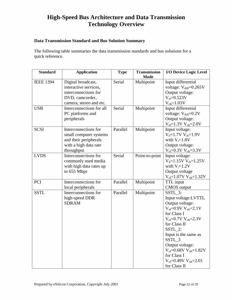
Data Transmission Standard and Bus Solution Summary The following table summaries the data transmission standards and bus solutions for a quick reference.
Standard Application Type Transmission Mode
I/O Device Logic Level
IEEE 1394 Digital broadcast, interactive services, interconnections for DVD, camcorder, camera, stereo and etc.
Serial
Multipoint Input differential voltage: Vdiff=0.265V Output voltage: Vol=0.523V Voh=1.03V
USB Interconnections for all PC platforms and peripherals
Serial Multipoint Input differential voltage: Vdiff=0.2V Output voltage: Vol=1.3V Voh=2.0V
SCSI Interconnections for small computer systems and their peripherals with a high data rate throughput
Parallel Multipoint Input voltage: Vil=1.7V Vih=1.9V with Vt=1.8V Output voltage: Vol=0.3V Voh=3.3V
LVDS Interconnections for commonly used media with high data rates up to 655 Mbps
Serial Point-to-point Input voltage: Vil=1.15V Vih=1.25V with Vt=1.2V Output voltage Vol=1.07V Voh=1.32V
PCI Interconnections for local peripherals
Parallel Multipoint TTL input CMOS output
SSTL Interconnections for high-speed DDR SDRAM
Parallel Multipoint SSTL_3: Input voltage:LVTTL Output voltage: Vol=0.9V Voh=2.1V for Class I Vol=0.7V Voh=2.3V for Class II SSTL_2: Input is the same as SSTL_3 Output voltage: Vol=0.68V Voh=1.82V for Class I Vol=0.49V Voh=2.01 for Class II

High-Speed Bus Architecture and Data Transmission Technology Overview
Prepared by eSilicon Corporation, Copyright July 2001 Page 23 of 29
Standard Application Type Transmission Mode
I/O Device Logic Level
GTL/GTL+ Interconnections between a processor and its memory modules on a board (GTL), GTL+ for a backplane bus
Parallel Multipoint Input threshold voltage Vt=0.8V (GTL+: 1V) Output voltage Vol=0.4V (GTL+: 0.55V) Termination voltage Vtt=1.2V (GTL+: 1.5V)
AGP High performance, component level interconnect targeted at 3D graphical display applications
Parallel Multipoint TTL input CMOS output
ATA/ATAPI Interconnections in modern hard disks for PCs and workstations
Parallel Multipoint TTL input CMOS output
I2C Internal IC control bus Serial Multipoint Input voltage Vil=0.3Vdd Vih=0.7Vdd Output voltage Vol=0.4V or 0.2Vdd (Vdd<2V)
SerDes Interface for point-to-point high-speed data transfer
Paralle-to-serial Serial-to-parallel
Point-to-point Paralle I/Os: 3V CMOS Serial I/Os: PECL/LVDS/CML

High-Speed Bus Architecture and Data Transmission Technology Overview
Prepared by eSilicon Corporation, Copyright July 2001 Page 24 of 29
Glossary Arbitration: The process by which nodes compete for ownership of the bus. The cable environment uses a hierarchical point-to-point algorithm, while the backplane environment uses the bit-serial process of transmitting an arbitration sequence. At the completion of an arbitration contest only one node will be able to transmit a data packet. Bandwidth: Maximum effective transfer rate for all of the channels. Baud: The signaling speed in transitions per second. Bit Error Ratio (BER): The statistical probability of a transmitted bit being erroneously received in a communication system. The BER is measured by counting the number of erroneous bits received and dividing by the total number of bits transmitted. Cable plant: All passive communications elements (e.g., optical fiber, connectors, splices, etc.) between a transmitter and a receiver. Channel: The path for a single signal of a parallel word. Channel adapter: Device that terminates a link and executes transport-level function. CML: Current mode logic. Connector: Device that connects the media to the transmitter or receiver. Cyclic Redundancy Check (CRC): Devices sending data use the CRC algorithm to calculate redundancy information from each block of data sent over the interface. This “CRC code” is sent along with the data. On the other end of the interface, the recipient of the data does the same CRC calculation and compares its result to the code the sender delivered. If there is a mismatch, this means the data was corrupted somehow and the block of data is resent. Data Payload: The data, not including any control or header information, carried in one packet. Disparity: The difference between the number of ones and zeros in a channel. DDR SDRAM: Double data rate synchronous dynamic random access memory. DMA: Direct memory access. Downstream: The direction of data flow from the host or away from the host.

High-Speed Bus Architecture and Data Transmission Technology Overview
Prepared by eSilicon Corporation, Copyright July 2001 Page 25 of 29
EIA: Electronic Industry Association. EMI: Electromagnetic interference. GTL: Gunning transceiver logic. GTL+ and GTLP are derivatives of GTL that operate at enhanced noise margin signal levels. GMII: Gigabit media independent interface. Host: One or more host channel adapters governed by a single memory/CPU complex. Host channel adapter (HCA): A channel adapter that supports the interface. Hub: A USB device that provides additional connections to the USB. Typical applications are parallel backplanes. HVD: High voltage differential. IIC: Inter-integrated circuit (an internal control bus). I/O: Input/Output. I/O controller: One of the two architectural divisions of an I/O unit. An I/O controller (IOC) provides I/O services, while a target channel adapter provides transport services. I/O unit: An I/O unit (IOU) provides I/O service(s). An I/O unit consists of one or more I/O controllers. Isochronous: The term isochronous indicates the essential characteristics of a time-scale or a signal such that the time intervals between consecutive significant instances either have the same duration or multiples of the shortest duration. InterSymbol Interference (ISI): ISI is caused by the time difference required for the signal to arrive at the receiver threshold when starting from different places in bit sequences (symbols). JEDEC: Joint Electronics Devices Engineering Council. Live Insertion/Removal: The ability to attach and remove devices while the system is in operation.

High-Speed Bus Architecture and Data Transmission Technology Overview
Prepared by eSilicon Corporation, Copyright July 2001 Page 26 of 29
Link layer: The layer, in a stack of three protocol layers defined for the serial bus, which provides the service to the transaction layer of one-way data transfer with confirmation of reception. The link layer provides addressing, data checking, and data framing. The link layer also provides an isochronous data transfer service directly to the application. LLC: Logic link control. LVDS: Low voltage differential signaling. LVTTL: Low voltage transistor-transistor logic. MAC: Media access control. NCITS: National Committee on Information Technology standards. Packet (1394): A serial stream of clocked data bits. Packet (USB): A bundle of data organized in a group for transmission. Packets typically contain three elements: control information (e.g. source, destination, and length), the data to be transferred, and error detection and correction bits. PCS: Physical coding sublayer. PMD: Physical layer media dependent. PCI: Peripheral Component Interconnect. Packet payload: The portion of packet between (not including) any transport header(s) and the CRCs at the end of each packet. The packet payload contains up to 4096 bytes. Port: A physical layer entity in a node that connects to either a cable or backplane and provides one end of physical connection with another node. Run length: Maximum number of consecutive identical bits in the transmitted signal, e.g., 0011111010 has a run length of five. Running disparity: A binary parameter indicating the cumulative disparity (positive or negative) of all previously issued bits. SCSI: Small computer system interface. SSTL: Stub series terminated logic. Stubs: Short traces, branching from the backplane. Often found on memory modules.

High-Speed Bus Architecture and Data Transmission Technology Overview
Prepared by eSilicon Corporation, Copyright July 2001 Page 27 of 29
Target channel adapter (TCA): A channel adapter typically used to support I/O devices. Termination resistor: The termination resistor is used at the end of a transmission line in order to avoid reflections of the transmitted signal. A line is optimally terminated if the termination resistor is chosen to be equal to the line impedance. TIA: Telecommunication Industry Association. Transaction: The delivery of service to an endpoint; consists of a token packet, optional data packet, and optional handshake packet. Special packets are allowed/required based on the transaction type. UI: Unit interval = 1 bit period. USB: Universal serial bus. Upstream: The direction of the data flow towards the host.

High-Speed Bus Architecture and Data Transmission Technology Overview
Prepared by eSilicon Corporation, Copyright July 2001 Page 28 of 29
References [1] “Comparing Bus Solutions”, Application Report, SLLA067, TI, March 2000 [2] “RapidIO European Symposium Technical Overview and Update”, April 2001 [3] “The Lightening Data Transport I/O Bus Architecture”, LDT I/O White Paper, revision #1001, API NetWorks, Inc. [4] InfiniBand Architecture Release 1.0, Volume 1- General Specifications, October 2000 [5] “Serial Interconnects for High Performance Computing”, Steve Paavola [6] EIA/TIA-232-E, ITU-T V.28 [7] EIA/TIA-485, Information Technology-Telecommunications and information exchange between systems-Twisted pair multi-point interconnection [8] EIA/TIA-644, Electrical Characteristics of Low Voltage Differential Signaling (LVDS) Interface Circuits [9] EIA/JESD8-3, Gunning Transceiver Logic (GTL), Low-Level, High-Speed Interface Standard for Digital Integrated Circuits [10] IEEE 1394-1995, High Performance Serial Bus [11] EIA/JESD8-8, Stub Series Terminated Logic for 3.3V (SSTL_3) [12] EIA/JESD8-9, Stub Series Terminated Logic for 2.5V (SSTL_2) [13] IEEE 802.3z Gigabit Task Force [14] GMII Gigabit Media Independent Interface [15] USB Universal Serial Bus Specification Revision 1.1 (Compaq, Intel, Microsoft, NEC) [16] T11.1/Project 1249-D/Rev 2.2, Information Technology-High-Performance Parallel Interface-6400 Mbit/s Optical Specification (HIPPI-6400-OPT) [17] “Overview of SCSI Standards & Cables”, SCSITA [18] T13/Project 1410-D/Rev 1a, Information Technology-AT Attachment with Packet Interface-6 (ATA/ATAPI-6)

High-Speed Bus Architecture and Data Transmission Technology Overview
Prepared by eSilicon Corporation, Copyright July 2001 Page 29 of 29
[19] “Integrated Drive Electronics/AT Attachment (IDE/ATA) interface”, Charles Kozierok [20] “Serial ATA, FAQ”, Serial ATA Working Group [21] AGP Accelerated Graphics Port Interface Specification Revision 2.0 (Intel) [22] PCI Local Bus Interface Specification Revision 2.2 (PCI SIG) [23] The I2C-Bus Specification, Version 2.1(Philips)