High-resolution scanning tunneling microscopy...
38
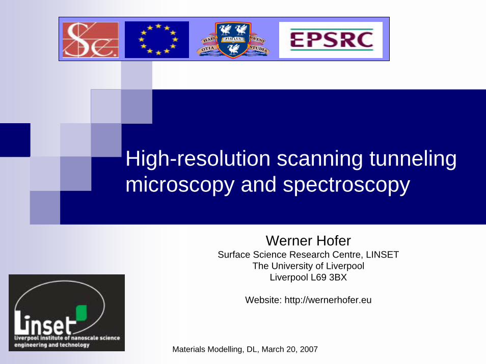
Materials Modelling, DL, March 20, 2007 High-resolution scanning tunneling microscopy and spectroscopy Werner Hofer Surface Science Research Centre, LINSET The University of Liverpool Liverpool L69 3BX Website: http://wernerhofer.eu
Transcript of High-resolution scanning tunneling microscopy...
Materials Modelling, DL, March 20, 2007
High-resolution scanning tunneling microscopy and spectroscopy
Werner HoferSurface Science Research Centre, LINSET
The University of LiverpoolLiverpool L69 3BX
Website: http://wernerhofer.eu
Materials Modelling, DL, March 20, 2007
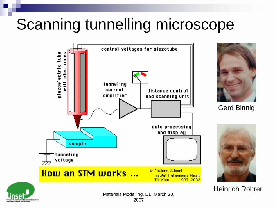
Scanning tunnelling microscope
Gerd Binnig
Heinrich Rohrer
Materials Modelling, DL, March 20, 2007
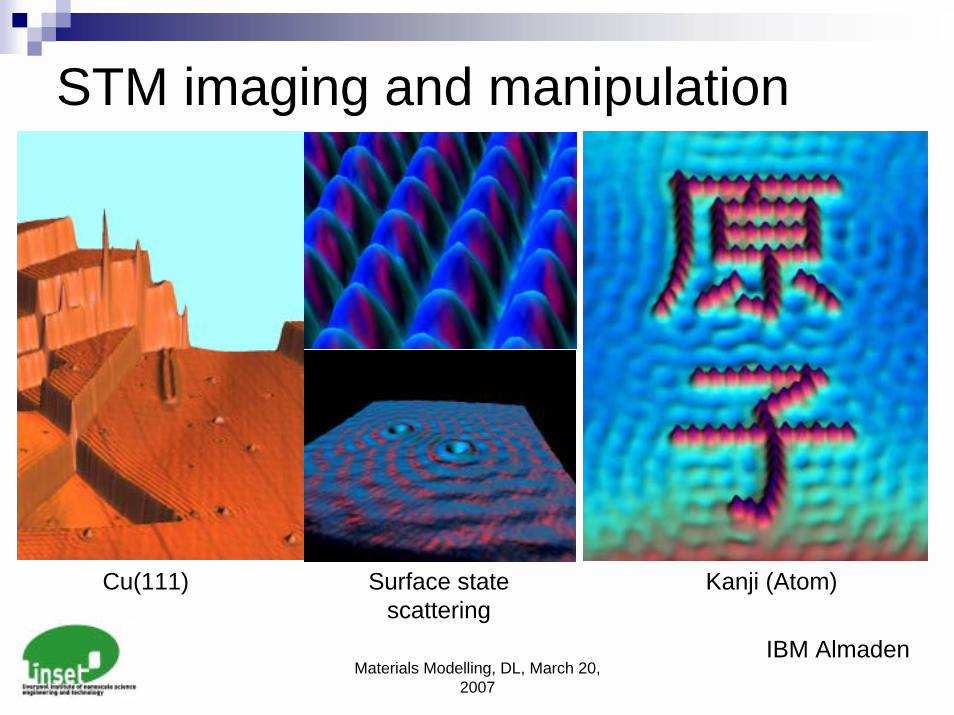
STM imaging and manipulation
Cu(111) Surface statescattering
Kanji (Atom)
IBM Almaden
Materials Modelling, DL, March 20, 2007
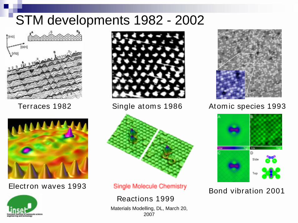
STM developments 1982 - 2002
Terraces 1982 Single atoms 1986 Atomic species 1993
Electron waves 1993Bond vibration 2001
Reactions 1999
Materials Modelling, DL, March 20, 2007
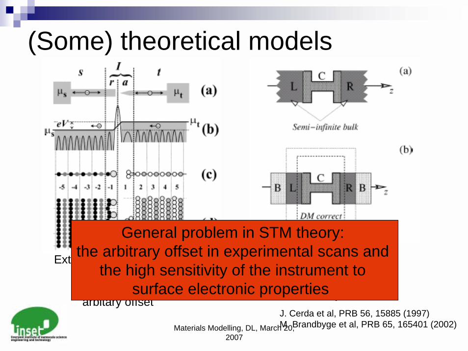
(Some) theoretical models
J. Cerda et al, PRB 56, 15885 (1997)M. Brandbyge et al, PRB 65, 165401 (2002)
Extended Huckel theory:coupled system,
local orbitals, arbitary offset
Keldysh formalism:coupled system,
local orbitals,no arbitrary offset
General problem in STM theory: the arbitrary offset in experimental scans and
the high sensitivity of the instrument to surface electronic properties
Materials Modelling, DL, March 20, 2007
! Theory! Tip Design! Local Spin Detection! Single Atom Contacts! Molecular Corrals! Outlook
Materials Modelling, DL, March 20, 2007
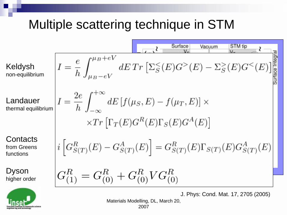
Multiple scattering technique in STM
Keldyshnon-equilibrium
Landauerthermal equilibrium
Contactsfrom Greens functions
Dysonhigher order
J. Phys: Cond. Mat. 17, 2705 (2005)
Materials Modelling, DL, March 20, 2007
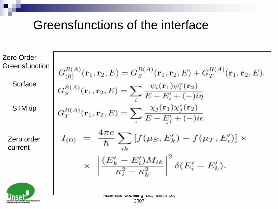
Greensfunctions of the interface
Zero OrderGreensfunction
Surface
STM tip
Zero ordercurrent
Materials Modelling, DL, March 20, 2007
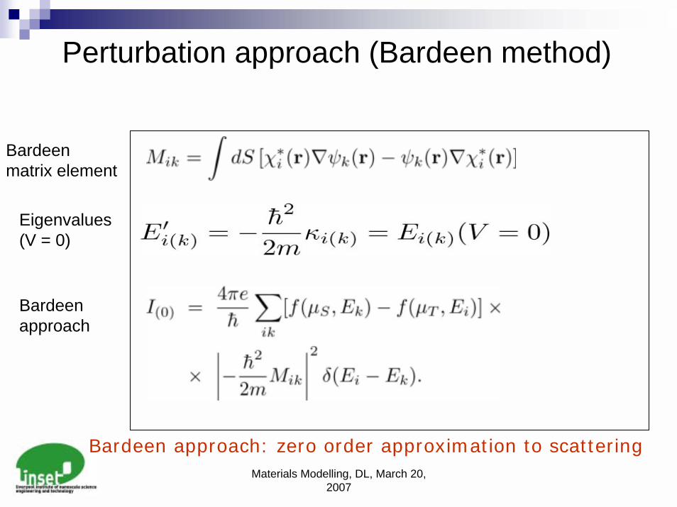
Perturbation approach (Bardeen method)
Bardeenmatrix element
Eigenvalues(V = 0)
Bardeenapproach
Bardeen approach: zero order approximation to scattering
Materials Modelling, DL, March 20, 2007
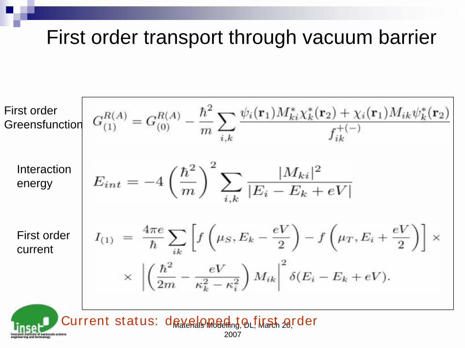
First order transport through vacuum barrier
First orderGreensfunction
Interactionenergy
First ordercurrent
Current status: developed to first order
Materials Modelling, DL, March 20, 2007
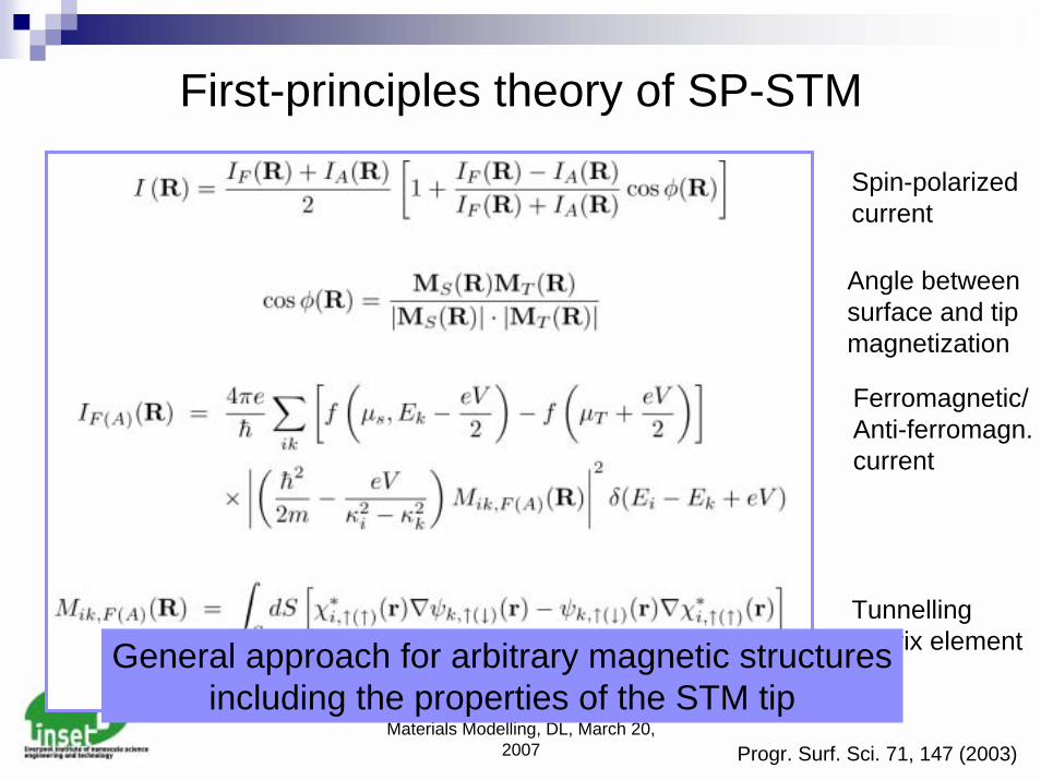
First-principles theory of SP-STM
Spin-polarizedcurrent
Angle betweensurface and tipmagnetization
Tunnellingmatrix element
Ferromagnetic/Anti-ferromagn.current
General approach for arbitrary magnetic structuresincluding the properties of the STM tip
Progr. Surf. Sci. 71, 147 (2003)
Materials Modelling, DL, March 20, 2007
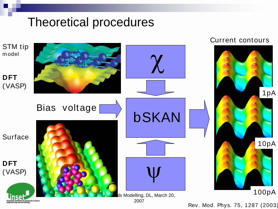
Theoretical proceduresCurrent contours
χSTM tipmodel
1pA
10pA
100pA
DFT(VASP)
bSKANBias voltage
Surface
ψDFT(VASP)
Rev. Mod. Phys. 75, 1287 (2003)
Materials Modelling, DL, March 20, 2007
The importance of efficient programming:
! Typical STM simulation:"No of k-points: 36"No of G-vectors: 100"No of gridpoints: > 1000"No of integrations: 362 x 1002 x 1000 = 1010
Required: highly efficient parallel code with minimum operations in the integration kernel. Development time: about three years
Required: large computer arrays
Materials Modelling, DL, March 20, 2007
Typical requirement for simulations
! Group of eight PostDocs/PhD students" Typical job profile: 8CPU/24-48hours" Typical number of jobs: 2/person" Typical CPU-hours/year: > 500000" Typical data storage: > 50Gb/person
! Data sharing:" Visual program output: OpenDX" Numbers: text files" Inputs: text files
Materials Modelling, DL, March 20, 2007
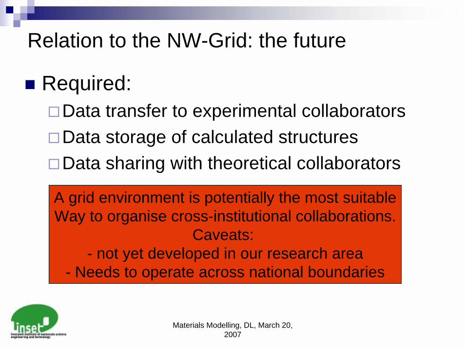
Relation to the NW-Grid: the future
! Required:"Data transfer to experimental collaborators"Data storage of calculated structures"Data sharing with theoretical collaborators
A grid environment is potentially the most suitableWay to organise cross-institutional collaborations.
Caveats: - not yet developed in our research area
- Needs to operate across national boundaries
Materials Modelling, DL, March 20, 2007
! Theory! Tip Design! Local Spin Detection! Single Adatom Contacts! Molecular Corrals! Outlook
Materials Modelling, DL, March 20, 2007
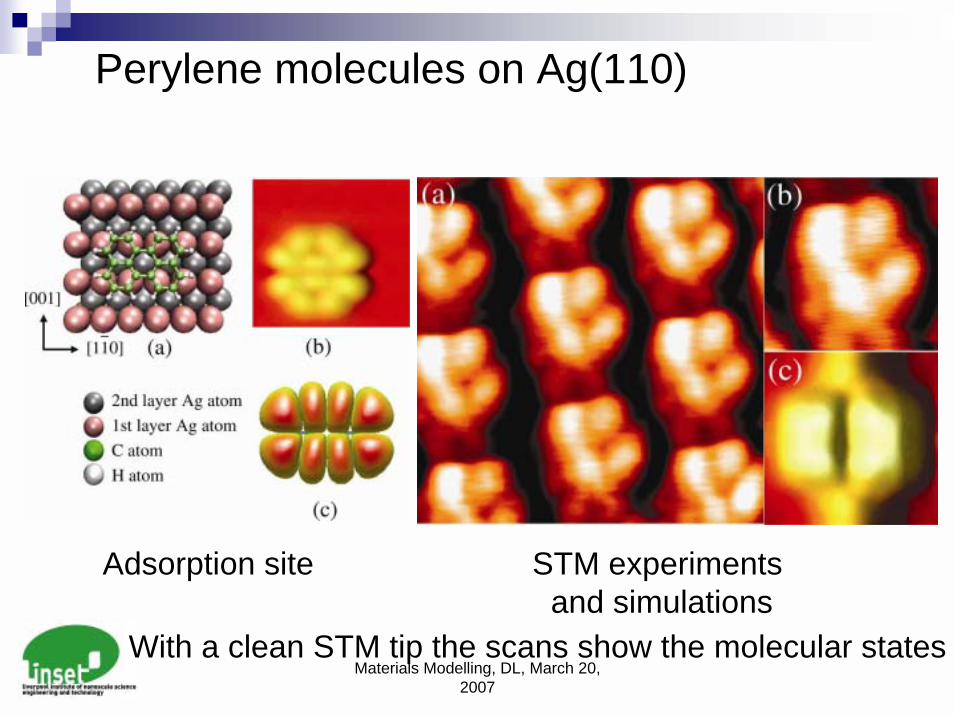
Perylene molecules on Ag(110)
Adsorption site STM experiments and simulations
With a clean STM tip the scans show the molecular states

Materials Modelling, DL, March 20, 2007
Functional STM tip
Perylene molecule adsorbedon a tungsten tip
A functional tip shows the statesof the clean silver surface
PRL 96, 156102 (2006)
Materials Modelling, DL, March 20, 2007
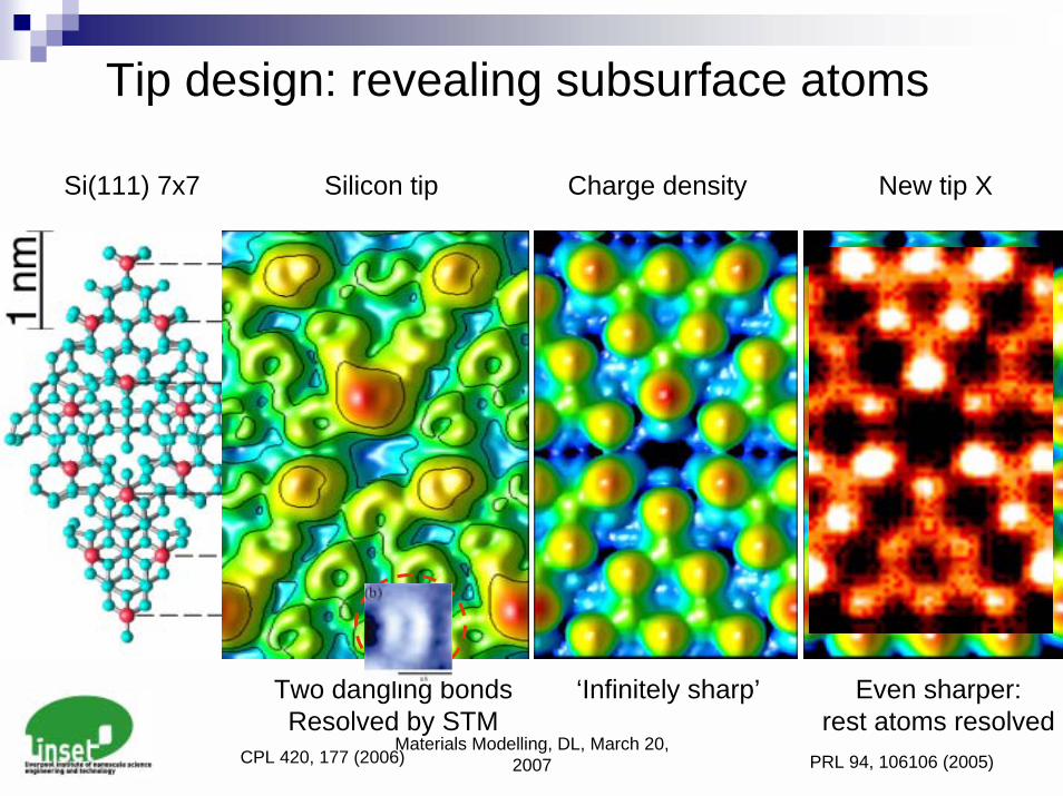
Tip design: revealing subsurface atoms
Si(111) 7x7 Silicon tip Charge density New tip X
‘Infinitely sharp’ Even sharper:rest atoms resolved
Two dangling bondsResolved by STM
CPL 420, 177 (2006) PRL 94, 106106 (2005)
Materials Modelling, DL, March 20, 2007
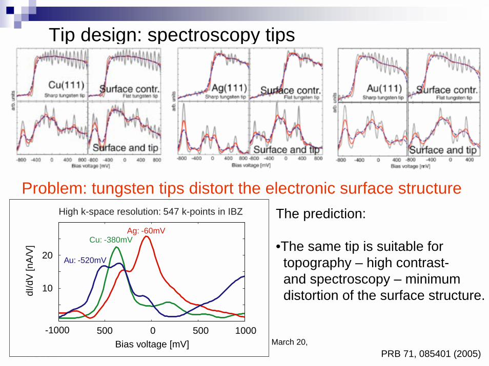
Tip design: spectroscopy tips
Problem: tungsten tips distort the electronic surface structure
PRB 71, 085401 (2005)
The prediction:
•The same tip is suitable for topography – high contrast-and spectroscopy – minimum distortion of the surface structure. 10
20
-1000 500 0 500 1000
dI/d
V [n
A/V
]
Bias voltage [mV]
Cu: -380mVAg: -60mV
Au: -520mV
High k-space resolution: 547 k-points in IBZ
Materials Modelling, DL, March 20, 2007
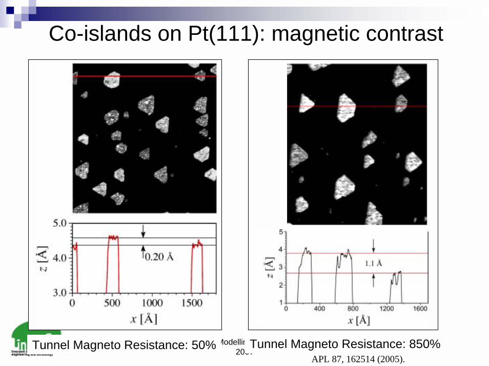
Co-islands on Pt(111): magnetic contrast
Tunnel Magneto Resistance: 50% Tunnel Magneto Resistance: 850%APL 87, 162514 (2005).
Materials Modelling, DL, March 20, 2007
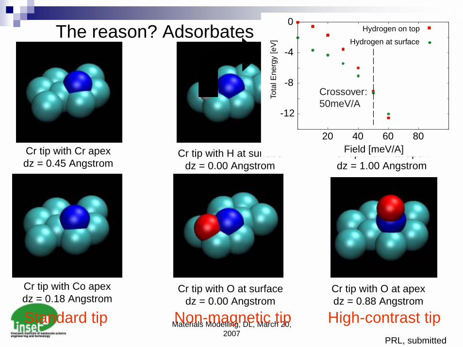
The reason? Adsorbates
Cr tip with Cr apexdz = 0.45 Angstrom
Cr tip with H at surfacedz = 0.00 Angstrom
Cr tip with H at apexdz = 1.00 Angstrom
-12
-8
-4
0
20 40 60 80
Tota
l Ene
rgy
[eV
]
Field [meV/A]
Hydrogen on top
Hydrogen at surface
Crossover:50meV/A
Cr tip with Co apexdz = 0.18 Angstrom
Standard tip Non-magnetic tip
Cr tip with O at surfacedz = 0.00 Angstrom
High-contrast tip
Cr tip with O at apexdz = 0.88 Angstrom
PRL, submitted
Materials Modelling, DL, March 20, 2007
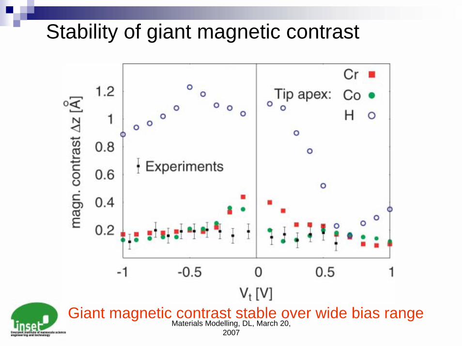
Stability of giant magnetic contrast
Giant magnetic contrast stable over wide bias range
Materials Modelling, DL, March 20, 2007
! Theory! Tip Design! Local Spin Detection! Single Adatom Contacts! Molecular Corrals! Outlook
Materials Modelling, DL, March 20, 2007
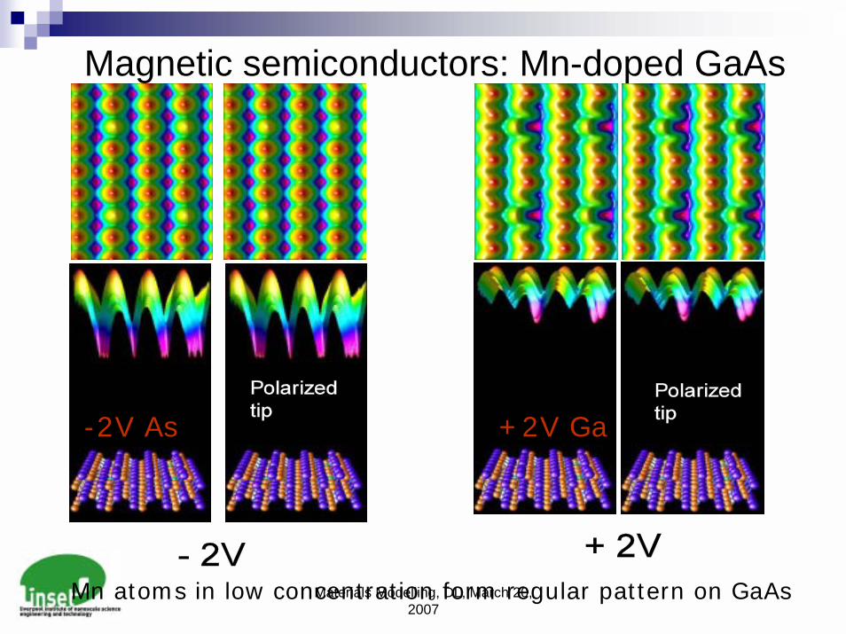
Magnetic semiconductors: Mn-doped GaAs
-2V As +2V Ga
Mn atoms in low concentration form regular pattern on GaAs
Materials Modelling, DL, March 20, 2007
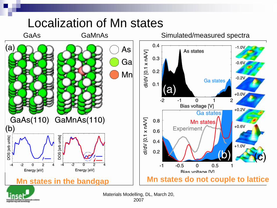
Localization of Mn statesGaAs GaMnAs Simulated/measured spectra
Mn states in the bandgap Mn states do not couple to lattice
Materials Modelling, DL, March 20, 2007
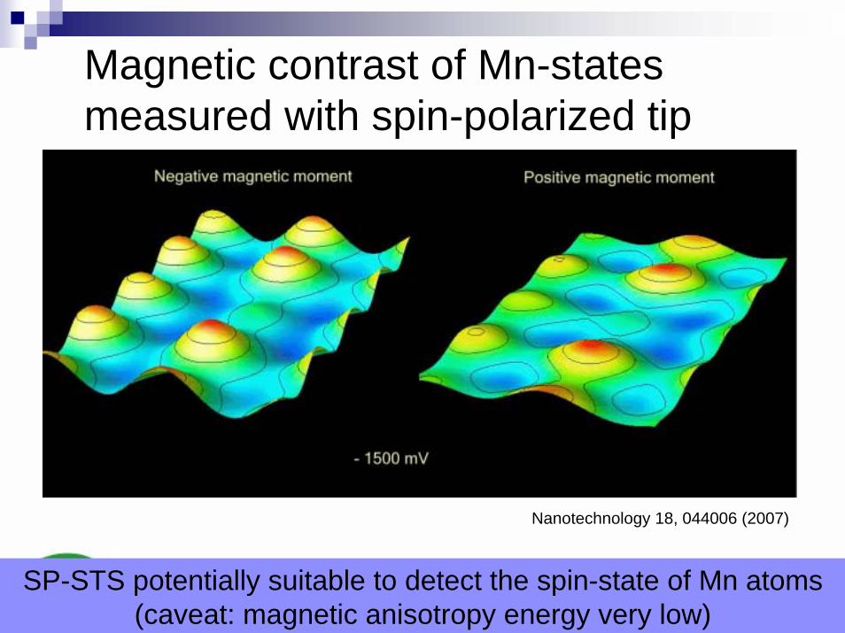
Magnetic contrast of Mn-states measured with spin-polarized tip
Nanotechnology 18, 044006 (2007)
SP-STS potentially suitable to detect the spin-state of Mn atoms(caveat: magnetic anisotropy energy very low)
Materials Modelling, DL, March 20, 2007
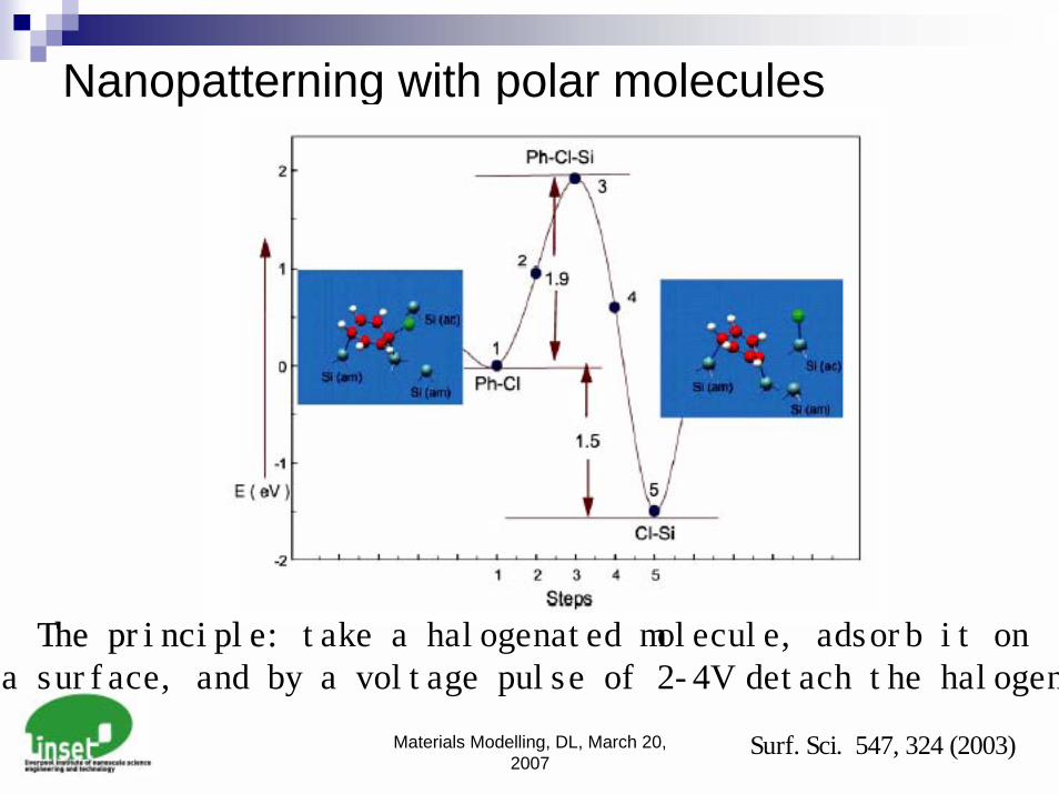
Nanopatterning with polar molecules
The principle: take a halogenated molecule, adsorb it ona surface, and by a voltage pulse of 2-4V detach the halogen
Surf. Sci. 547, 324 (2003)
Materials Modelling, DL, March 20, 2007
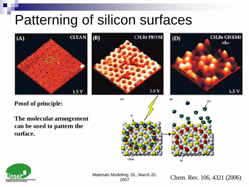
Patterning of silicon surfaces
Proof of principle:
The molecular arrangementcan be used to pattern thesurface.
Chem. Rev. 106, 4321 (2006)
Materials Modelling, DL, March 20, 2007
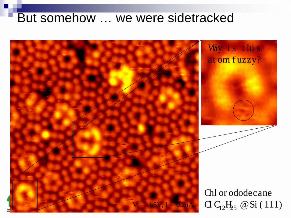
But somehow … we were sidetracked
Where is this atom?
Why is thisatom fuzzy?
ChlorododecaneClC12H25 @ Si(111)V = -1.5V, I = 0.2nA
Materials Modelling, DL, March 20, 2007
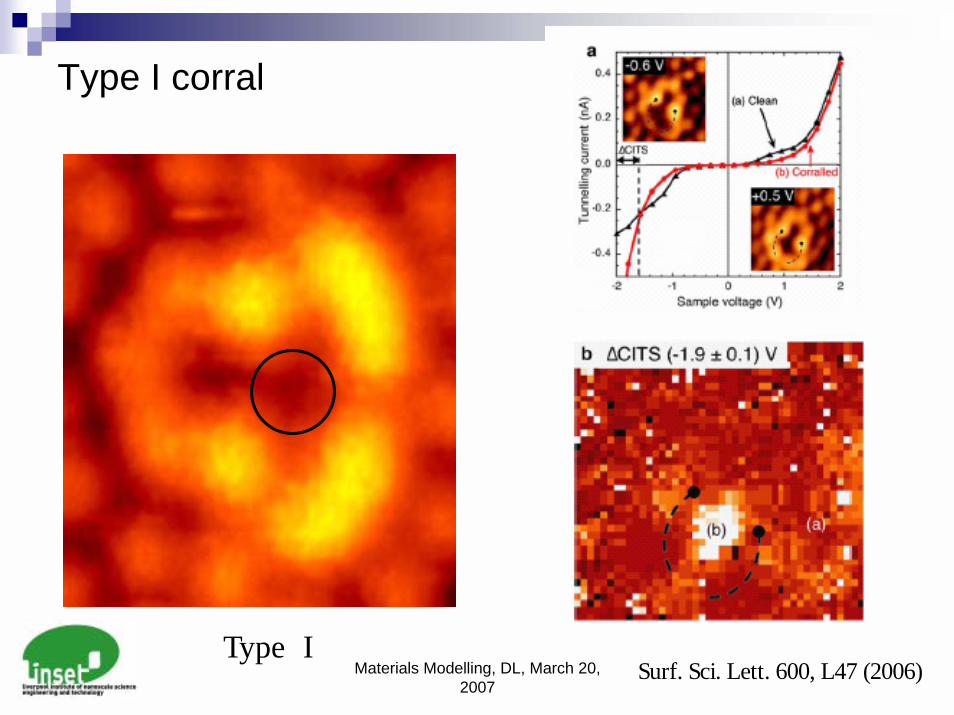
Type I corral
Type ISurf. Sci. Lett. 600, L47 (2006)
Materials Modelling, DL, March 20, 2007
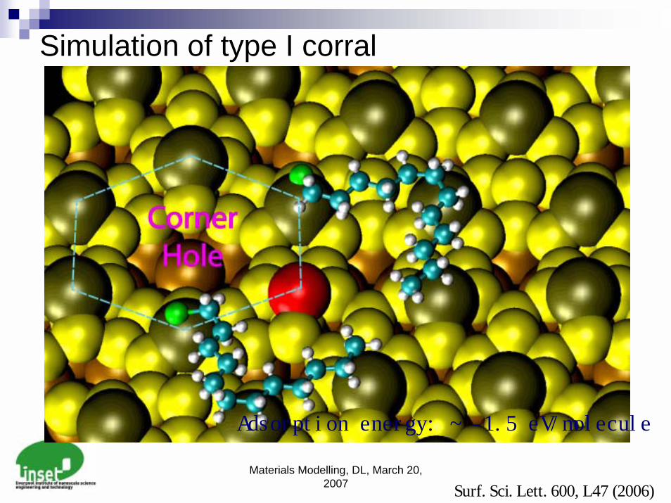
Simulation of type I corral
Adsorption energy: ~ -1.5 eV/molecule
Surf. Sci. Lett. 600, L47 (2006)
Materials Modelling, DL, March 20, 2007
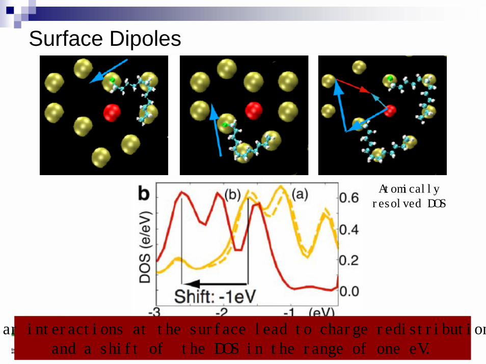
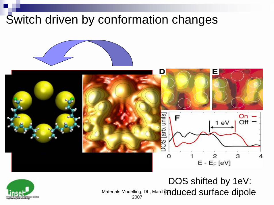
Surface Dipoles
lar interactions at the surface lead to charge redistributionand a shift of the DOS in the range of one eV.
Atomicallyresolved DOS
Materials Modelling, DL, March 20, 2007
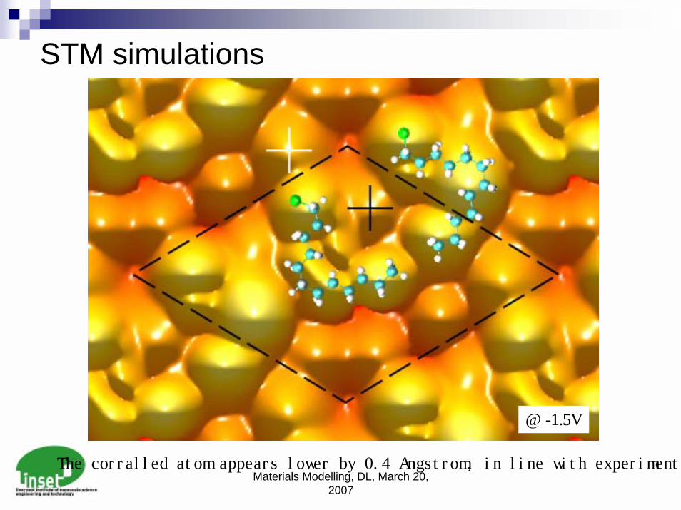
STM simulations
@ -1.5V
The corralled atom appears lower by 0.4 Angstrom, in line with experiments
Materials Modelling, DL, March 20, 2007
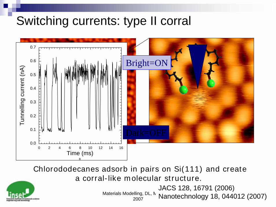
Switching currents: type II corral
0.0
0.1
0.2
0.3
0.4
0.5
0.6
0.7
0 2 4 6 8 10 12 14 16
Tunn
ellin
g cu
rren
t (nA
)
B
Time (ms)
Bright=ON
Dark=OFF
Chlorododecanes adsorb in pairs on Si(111) and createa corral-like molecular structure.
JACS 128, 16791 (2006)Nanotechnology 18, 044012 (2007)
Materials Modelling, DL, March 20, 2007
Switch driven by conformation changes
DOS shifted by 1eV:Induced surface dipole
Materials Modelling, DL, March 20, 2007
Outlook
! Multiple scattering through an interface
! STM induced photon emission
! Design of tips for optimum performance

Materials Modelling, DL, March 20, 2007
Thank you for your attention