High resolution CdTe imaging devices for a Semiconductor ...€¦ · Designing analog LSI also by...

1
Designing analog LSI also by ourselves Takefumi Mitani 1,2 , T. Tanaka 1,2 , Y. Kobayashi 1,2 , H. Inoue 1,2 , K. Nakazawa 1 , T. Takahashi 1,2 , H.Tajima 3 , Y. Fukazawa 4 , S. Uno 4 , M. Nomachi 5 , H. Nakamura 5 , Y. Kuroda 6 , M. Onishi 6 30cm 10cm High resolution CdTe imaging devices for a Semiconductor Multi-Compton Telescope High energy Fine position High timing For high sensitivity with SMCT, 1024ch CdTe Array detector for balloon-borne, satellite-borne experiments High performance of the combination of analog LSI “VA32TA” + CdTe pixel Absorber Scatterer FEC control, A/D conversion and construct data packets Data acquisition system Semiconductor Multi-Compton Telescope ( SMCT ) resolution are essential 1 . To realize SMCT, we are developing three new technologies We have developed a low noise analog LSI, “VA32TA2 , and combined it with CdTe pixel detector. Preamp and 2 shapers, one for Spectroscopy and one for self trigger Serial I/O (Space wire) Two M8 nuts image obtained with 57Co using half of the detector. 4.9 mm Bias: 600V 241 Am 0 o C Best spectrum Bias: 600V ΔE = 1.7keV(FWHM) @ 60keV, 0 o C ¸2003 model (CAST-H01, CAST-T01) 2-dimensional pixel LSI ( spectroscopy and photo counting ) CdTe diode with 2 mm square pixels 18mm 1 Institute of Space and Astronautical Science, Japan, 2 University of Tokyo, Japan, 3 SLAC, 4 Hiroshima University, 5 Osaka University, 6 Mitsubishi Heavy Industries Co., Ltd A new generation of Compton Telescope, based on semiconductor material, is believed to bring a breakthrough in the observation of the gamma-ray universe. To realize the Semiconductor Multi-Compton Telescope(SMCT), we have been working on the development of the semiconductor material and the readout system. In the Compton Camera, the incident angle of photon is calculated as e.g. So the energy resolution is the key factor to improve not only sensitivity to detect gamma-ray lines but also the angular resolution. CdTe diode: has a high energy resolution and detection efficiency of gamma-ray. See Tanaka’s poster Low noise analog LSI: to fullly utilize semiconductor and achieve high energy resolution. Multi channel readout system: Compact (weight and power) system is required for balloon-borne satellite-borne experiments. VA32TA 32 channel signal processing 7mm 3.4mm ¸Low noise; Front-end MOSFET geometry optimized for small capacitance load. ¸Need only 1 bias (adopting internal DACs) ¸Variable shaping time (slow shaper: 1-4 μsec, fast shaper: 75nsec or 300nsec) ¸Radiation torelant to 20Mrad Front end card(FEC) 2.5cm Two VA32TAs are mounted on 1 FEC. A small number of passive component are used for filtering. FEC and CdTe diode We obtained uniform 57 Co spectra at +20 o C Using the FECs, we have developed a compact readout system based on CPLD technology 3 . The schematic diagram of the readout system is as follows. CdTe array 16 FECs Readout card(ROC) Interface card(IFC) 1024 individual CdTe detectors. We adopted “edge-on” geometry for high detection efficiency. 1.2mm 5mm 5 mm CdTe has detection efficiency of 20% at 300keV. Total power: 10W To establish an OPEN IP for the high performance analog VLSI, we are working on the IN-HOUSE ASIC development at ISAS based on 0.35μm rule. Reference: 1. SPIE 2002 Takahashi et. al, 2. SPIE 2002 Tajima et. al, 3. IEEE 2003 Mitani et. al E-mail: [email protected] Charge sensitive amplifier Peak hold circuit Shaping amp Discriminator Input Output Pole-zero cancellation Level adapter and trigger controller 22mm 44mm ¸2002 model (CAST-K01) (0.37 +0.16 ¥ C)/ t [keV] ΔE = 2.5keV (FWHM) on an average @ 122keV +20 o C Monitor Shaper out 7 channels was not connected properly to CdTe pixels. In the next version, all channels’ connection was OK. Single elements of 1024-array detector Fan out board VA32TA

Transcript of High resolution CdTe imaging devices for a Semiconductor ...€¦ · Designing analog LSI also by...

Designing analog LSI also by ourselves

Takefumi Mitani1,2, T. Tanaka1,2, Y. Kobayashi1,2, H. Inoue1,2, K. Nakazawa1, T. Takahashi1,2, H.Tajima3, Y. Fukazawa4, S. Uno4, M. Nomachi5, H. Nakamura5, Y. Kuroda6, M. Onishi6

30cm

10cm

High resolution CdTe imaging devices for a Semiconductor Multi-Compton Telescope

High energyFine positionHigh timing

For high sensitivity with SMCT,

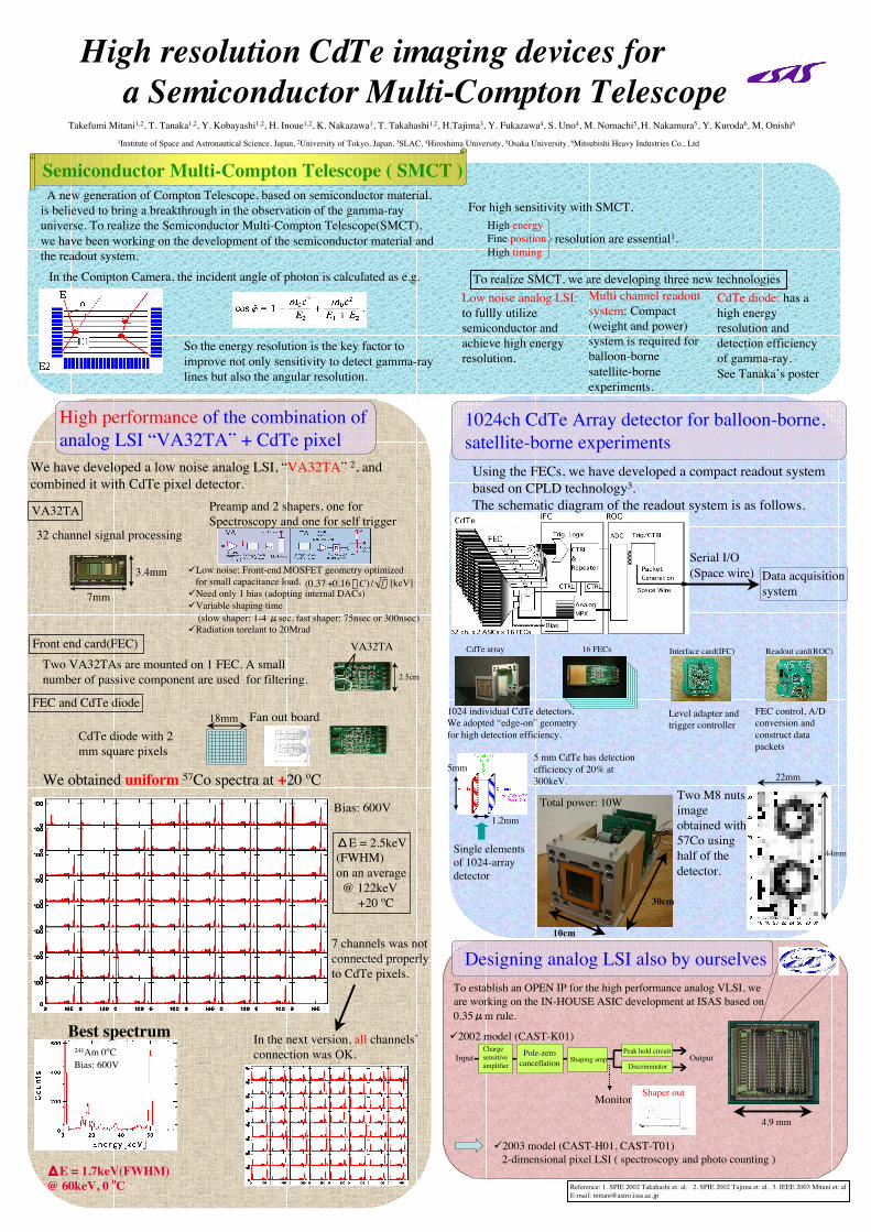
1024ch CdTe Array detector for balloon-borne,satellite-borne experiments

High performance of the combination ofanalog LSI “VA32TA” + CdTe pixel

Absorber

Scatterer

FEC control, A/Dconversion andconstruct datapackets

Data acquisitionsystem

Semiconductor Multi-Compton Telescope ( SMCT )

resolution are essential1.

To realize SMCT, we are developing three new technologies

We have developed a low noise analog LSI, “VA32TA” 2, andcombined it with CdTe pixel detector.

Preamp and 2 shapers, one for Spectroscopy and one for self trigger

Serial I/O(Space wire)

Two M8 nutsimageobtained with57Co usinghalf of thedetector.

4.9 mm

Bias: 600V

241Am 0oC

Best spectrum

Bias: 600V

ΔE = 1.7keV(FWHM) @ 60keV, 0 oC

¸2003 model (CAST-H01, CAST-T01) 2-dimensional pixel LSI ( spectroscopy and photo counting )

CdTe diode with 2mm square pixels

18mm

1Institute of Space and Astronautical Science, Japan, 2University of Tokyo, Japan, 3SLAC, 4Hiroshima University, 5Osaka University, 6Mitsubishi Heavy Industries Co., Ltd

A new generation of Compton Telescope, based on semiconductor material,is believed to bring a breakthrough in the observation of the gamma-rayuniverse. To realize the Semiconductor Multi-Compton Telescope(SMCT),we have been working on the development of the semiconductor material andthe readout system.

In the Compton Camera, the incident angle of photon is calculated as e.g.

So the energy resolution is the key factor toimprove not only sensitivity to detect gamma-raylines but also the angular resolution.

CdTe diode: has ahigh energyresolution anddetection efficiencyof gamma-ray.See Tanaka’s poster

Low noise analog LSI:to fullly utilizesemiconductor andachieve high energyresolution.

Multi channel readoutsystem: Compact(weight and power)system is required forballoon-bornesatellite-borneexperiments.

VA32TA

32 channel signal processing

7mm

3.4mm ¸Low noise; Front-end MOSFET geometry optimized for small capacitance load.¸Need only 1 bias (adopting internal DACs)¸Variable shaping time (slow shaper: 1-4 μsec, fast shaper: 75nsec or 300nsec)¸Radiation torelant to 20Mrad

Front end card(FEC)

2.5cmTwo VA32TAs are mounted on 1 FEC. A smallnumber of passive component are used for filtering.

FEC and CdTe diode

We obtained uniform 57Co spectra at +20 oC

Using the FECs, we have developed a compact readout systembased on CPLD technology3.The schematic diagram of the readout system is as follows.

CdTe array 16 FECs Readout card(ROC)Interface card(IFC)

1024 individual CdTe detectors.We adopted “edge-on” geometryfor high detection efficiency.

1.2mm

5mm5 mm CdTe has detectionefficiency of 20% at300keV.

Total power: 10W

To establish an OPEN IP for the high performance analog VLSI, weare working on the IN-HOUSE ASIC development at ISAS based on0.35μm rule.

Reference: 1. SPIE 2002 Takahashi et. al, 2. SPIE 2002 Tajima et. al, 3. IEEE 2003 Mitani et. alE-mail: [email protected]

Chargesensitiveamplifier

Peak hold circuitShaping amp

DiscriminatorInput OutputPole-zero

cancellation

Level adapter andtrigger controller

22mm

44mm

¸2002 model (CAST-K01)

(0.37 +0.16 ¥ C) / t [keV]

ΔE = 2.5keV(FWHM)on an average @ 122keV +20 oC

Monitor Shaper out

7 channels was notconnected properlyto CdTe pixels.

In the next version, all channels’connection was OK.

Single elementsof 1024-arraydetector

Fan out board

VA32TA