
High Quality Gate Dielectric/MoS2 Interfaces Probed by the ...
63
University of Central Florida University of Central Florida STARS STARS Electronic Theses and Dissertations 2018 High Quality Gate Dielectric/MoS2 Interfaces Probed by the High Quality Gate Dielectric/MoS2 Interfaces Probed by the Conductance Method Conductance Method Adithi Pandrahal Krishnaprasad Sharada University of Central Florida Part of the Electrical and Electronics Commons Find similar works at: https://stars.library.ucf.edu/etd University of Central Florida Libraries http://library.ucf.edu This Masters Thesis (Open Access) is brought to you for free and open access by STARS. It has been accepted for inclusion in Electronic Theses and Dissertations by an authorized administrator of STARS. For more information, please contact [email protected]. STARS Citation STARS Citation Krishnaprasad Sharada, Adithi Pandrahal, "High Quality Gate Dielectric/MoS2 Interfaces Probed by the Conductance Method" (2018). Electronic Theses and Dissertations. 5989. https://stars.library.ucf.edu/etd/5989
Transcript of High Quality Gate Dielectric/MoS2 Interfaces Probed by the ...

University of Central Florida University of Central Florida
STARS STARS
Electronic Theses and Dissertations
2018
High Quality Gate Dielectric/MoS2 Interfaces Probed by the High Quality Gate Dielectric/MoS2 Interfaces Probed by the
Conductance Method Conductance Method
Adithi Pandrahal Krishnaprasad Sharada University of Central Florida
Part of the Electrical and Electronics Commons
Find similar works at: https://stars.library.ucf.edu/etd
University of Central Florida Libraries http://library.ucf.edu
This Masters Thesis (Open Access) is brought to you for free and open access by STARS. It has been accepted for
inclusion in Electronic Theses and Dissertations by an authorized administrator of STARS. For more information,
please contact [email protected].
STARS Citation STARS Citation Krishnaprasad Sharada, Adithi Pandrahal, "High Quality Gate Dielectric/MoS2 Interfaces Probed by the Conductance Method" (2018). Electronic Theses and Dissertations. 5989. https://stars.library.ucf.edu/etd/5989

HIGH QUALITY GATE DIELECTRIC/MoS2 INTERFACES PROBED BY THE
CONDUCTANCE METHOD
by
ADITHI PANDRAHALLY KRISHNAPRASAD SHARADA
B.E. Visvesvaraya Technological University, 2015
A thesis submitted in partial fulfilment of the requirements
for the degree of Master of Science
in the Department of Electrical Engineering and Computer Science
in the College of Engineering and Computer Science
at the University of Central Florida
Orlando, Florida
Summer Term
2018

ii
© 2018 Adithi Pandrahally Krishnaprasad Sharada

iii
ABSTRACT
Two-dimensional materials provide a versatile platform for various electronic and optoelectronic
devices, due to their uniform thickness and pristine surfaces. We probe the superior quality of
2D/2D and 2D/3D interfaces by fabricating molybdenum disulfide (MoS2)-based field effect
transistors having hexagonal boron nitride (h-BN) and Al2O3 as the top gate dielectrics. An
extremely low trap density of ~71010 states/cm2-eV is extracted at the 2D/2D interfaces with h-
BN as the top gate dielectric on the MoS2 channel. 2D/3D interfaces with Al2O3 as the top gate
dielectric and SiOx as the nucleation layer exhibit trap densities between 71010 and 1011
states/cm2-eV, which is lower than previously reported 2D-channel/high--dielectric interface trap
densities. The comparable values of trap time constants for both interfaces imply that similar types
of defects contribute to the interface traps. This work establishes the case for van der Waals
systems where the superior quality of 2D/2D and 2D/high- dielectric interfaces can produce high
performance electronic and optoelectronic devices.

iv
ACKNOWLEDGMENTS
I would like to thank my advisor Dr. Tania Roy for her unwavering trust and support which
always encouraged me to work better. I would like to thank Dr. Reza Abdolvand and Dr. Jiann
Shiun Yuaan for being on my committee and for their valuable insights in my research.
I would like to thank my colleagues Hirokjyoti kalita, Sonali Das, Durjoy Dev and Nitin
Choudhary for their support throughout my Masters. I also would like to thank Teja Kothamsu
from Keysight Technologies for helping me in the measurements setup.
This work would not have been possible if it wasn’t for the support of my friends- Swathi,
Nandakishore, Kishan, Archana and Vyshakh. Thanks for believing in me and helping me
throughout this journey.
Last but not the least I would like to thank my dad Krishnaprasad, brother Akshay, uncle
Kanthareddy and my entire family for their never-ending love and support.

v
TABLE OF CONTENTS
LIST OF FIGURES ..................................................................................................................... viii
LIST OF TABLES ......................................................................................................................... xi
CHAPTER 1: INTRODUCTION TO 2D MATERIALS ............................................................... 1
1.1 Transition metal dichalcogenides (TMDC)........................................................................... 1
1.1.1 Crystal Structure of TMDC ............................................................................................ 2
1.1.2 2D Materials as Next Generation Channel Material ...................................................... 3
1.2 Interface states in 2D materials ............................................................................................. 4
1.2.1 Interface states ................................................................................................................ 4
1.2.2 Interface Trapped Charges .............................................................................................. 5
1.2.3 Origin of Interface states in 2D materials ....................................................................... 6
1.3 Objective of the Thesis .......................................................................................................... 7
1.4 Overview of thesis ................................................................................................................. 7
CHAPTER 2: THE CONDUCTANCE METHOD ........................................................................ 8
2.1 Dit Extraction Techniques ..................................................................................................... 8
2.1.1 Low frequency Method (Quasi-static C-V) .................................................................... 8
2.1.2 Castagné and Vapille method ......................................................................................... 9
2.1.3 Terman Method .............................................................................................................. 9
vi
2.1.4 Gray-Brown Method..................................................................................................... 10
2.2 Conductance technique for Dit extraction ........................................................................... 10
2.3 Advantages of Conductance technique ............................................................................... 15
2.4 Literature on 𝑫𝒊𝒕 characterization of MoS2 ........................................................................ 15
2.5 Chapter Summary ................................................................................................................ 17
CHAPTER 3: MoS2 FET DEVICE FABRICATION .................................................................. 19
3.1 Device Structure .................................................................................................................. 19
3.1.1 Device Schematic ......................................................................................................... 19
3.1.2 Scanning Electron Microscopy (SEM) of MoS2 FET .................................................. 20
3.1.3 Transmission Electron Microscopy (TEM) of MoS2 FET ........................................... 21
3.2 Fabrication procedure .......................................................................................................... 22
3.2.1 Alignment marks patterning using photolithography ................................................... 22
3.2.2 Mechanical Exfoliation of MoS2 flakes........................................................................ 23
3.2.3 Back-gated MoS2 FET fabrication ................................................................................ 23
3.2.4 Top-gated MoS2 FET fabrication ................................................................................. 24
3.3 Chapter Summary ................................................................................................................ 25
CHAPTER 4: EXPERIMENTAL RESULTS .............................................................................. 26
4.1 Pristine device characteristics ............................................................................................. 26
4.1.1 Current-Voltage (I-V) Characteristics .......................................................................... 26
4.1.2 C-V and G-V characteristics ......................................................................................... 29
vii
4.1.3 Dit extraction for pristine devices using the conductance technique ............................ 34
4.2 Effect of forming gas annealing .......................................................................................... 39
4.2.1 I-V Characteristics post FGA ....................................................................................... 40
4.2.2 Post FGA C-V and G-V characteristics ........................................................................ 41
4.2.3 Post FGA Dit extraction by conductance method ......................................................... 43
4.3 Chapter Summary ................................................................................................................ 46
CHAPTER 5: CONCLUSION ..................................................................................................... 47
5.1 Future Scope ........................................................................................................................ 47
REFERENCES ............................................................................................................................. 48

viii
LIST OF FIGURES
Figure 1: Periodic table depicting the TMDC library available with highlighted fields for chalcogen
and transition metal atoms. ............................................................................................... 2
Figure 2: Crystal structure of MoS2. ............................................................................................... 3
Figure 3: Figure showing surface morphology comparison of 3D and 2D semiconductors. ......... 4
Figure 4: Capacitance stretch-out observed in the MOS-C with the presence of interface states. . 6
Figure 5 : Equivalent circuits used for implementing conductance techniques. (a) simplified MOS-
C circuit for conductance measurements. (b) simplified circuit derived from (a). (c)
measurement circuit. (d) measurement circuit including the tunnel conductance and 𝐺𝑡
and series resistance 𝑟𝑠. .................................................................................................. 11
Figure 6 : 𝐺𝑃𝜔 v/s 𝜔 plot obtained from the equation 2.7 (single level) and 2.8 (continuum) and
the experimental data. ..................................................................................................... 13
Figure 7 : Device schematic of MoS2/h-BN FET. ........................................................................ 20
Figure 8 : Optical microscope image of MoS2/h-BN device. ....................................................... 20
Figure 9 : SEM image of the MoS2/h-BN device. ........................................................................ 21
Figure 10 : cross sectional TEM of a representative monolayer MoS2 FET with h-BN dielectric.
........................................................................................................................................ 22
Figure 11 : Back-gated I-V of MoS2 FET. Inset: The device on which the back-gated I-V
characterization was performed. ..................................................................................... 26
Figure 12 : Transfer characteristics of top-gated MoS2 /Al2O3 device with AlOx seeding layer. . 27
Figure 13 : Top-gated transfer characteristics of MoS2 /Al2O3 device with SiOx seeding layer. . 28
Figure 14 : Top-gated transfer characteristics of MoS2 FET with h-BN dielectric. ..................... 28

ix
Figure 15 : Capacitance model for the MoS2 FET. ....................................................................... 29
Figure 16 : C-V plots for pristine MoS2 FET with AlOx/Al2O3 gate dielectric. ........................... 30
Figure 17 : C-V plots for pristine MoS2 FET with SiOx/Al2O3 gate dielectric. ............................ 31
Figure 18 : Pristine C-V plots for h-BN dielectric device. ........................................................... 32
Figure 19 : G-V characteristics for pristine MoS2 FET with AlOx/Al2O3 gate dielectric. ............ 33
Figure 20 : G-V characteristics for pristine MoS2 FET with SiOx/Al2O3 gate dielectric. ............. 33
Figure 21 : G-V characteristics for pristine MoS2 FET with h-BN gate dielectric. ...................... 34
Figure 22 : G/–f curves for gate voltages varied from depletion to accumulation for pristine MoS2
FET with AlOx seeding layer. ........................................................................................ 36
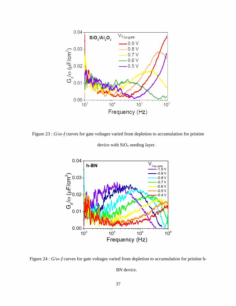
Figure 23 : G/–f curves for gate voltages varied from depletion to accumulation for pristine
device with SiOx seeding layer. ...................................................................................... 37
Figure 24 : G/–f curves for gate voltages varied from depletion to accumulation for pristine h-
BN device. ...................................................................................................................... 37
Figure 25 : Dit v/s trap position for the pristine Al2O3 and h-BN devices. .................................... 38
Figure 26 : Trap time constants v/s trap position for the pristine Al2O3 and h-BN devices.......... 39
Figure 27 : Post FGA transfer characteristics for MoS2 FET with Al2O3 gate dielectric with SiOx
seeding layer. Inset : Transfer characteristics for MoS2/h-BN device. .......................... 40
Figure 28 : Post FGA C-V and G-V characteristics of SiOx/Al2O3 device showing relatively
reduced frequency dispersion in the depletion region .................................................... 42
Figure 29 : Post FGA C-V and G-V characteristics of h-BN device showing relatively reduced
frequency dispersion in the depletion region .................................................................. 43
Figure 30 : Post FGA G/–f curves for gate voltages varied from depletion to accumulation in an
MoS2 FET with SiOx/Al2O3 gate dielectric and h-BN gate dielectric. ........................... 44

x
Figure 31 : Post FGA Dit v/s trap position exhibiting the decrease in the Dit for the SiOx/Al2O3 and
h-BN devices. ................................................................................................................. 45

xi
LIST OF TABLES
Table 1: Dit values for MoS2-based devices reported in literature………………………………16
1
CHAPTER 1: INTRODUCTION TO 2D MATERIALS
The scaling of silicon has reached its saturation making Moore’s law obsolete. Increased
rates of data transfer and performance are the main advantages of transistor scaling. But this
transistor scaling comes at a price of pronounced short channel effects, such as increased leakage
current, high static power dissipation etc.[1] Because of these aforementioned reasons, substitutes
for conventional channel material becomes very critical. Numerous technologies have been studied
for decades. With the isolation of single layer of graphene in 2004, two dimensional (2D) materials
gained widespread recognition. Graphene is a 2D semi-metallic material with very high carrier
mobility >50000 cm2/V-s at room temperature having applications in high-speed electronic
devices.[2, 3] However, the absence of band-gap in graphene i.e, the absence of OFF state in the
graphene field effect transistors (g-FETs) has inspired further exploration of layered materials.
Hence, other groups of 2D materials, such as Transitional metal dichalcogenides (TMDCs),
hexagonal boron nitride (h-BN), black phosphorus etc. which possess a bandgap have gained
prominence in electronic and optoelectronic applications. In this chapter, we discuss TMDCs in
detail, with an emphasis on interface states in these 2D materials.
1.1 Transition metal dichalcogenides (TMDC)
The library of TMDCs consists of several members - MoS2, WS2, MoSe2, WSe2, MoTe2,
WTe2, etc. which is aptly described in the periodic table as shown in the Figure 1.[4] The family
of TMDCs offer various materials ranging from semiconductors (MoS2, WSe2), metals (TaS2) and
superconductors (FeSe, NbSe2). Moreover, the bandgaps of these materials are tunable with the
number of layers. For example, monolayer MoS2 has a bandgap of 1.8 eV, with its bandgap

2
decreasing with increasing layer numbers. Multilayer MoS2 has a bandgap of 1.2 eV. Also, most
of these TMDCs are direct bandgap at the monolayer level, and become indirect bandgap
semiconductors with increasing layer numbers.
Figure 1: Periodic table depicting the TMDC library available with highlighted fields for
chalcogen and transition metal atoms.
1.1.1 Crystal Structure of TMDC
2D materials consist of a layer of transition metal M bounded to two layers of chalcogen
atom X forming MX2 which can be semi-conducting, super-conducting or semi-metallic in nature.

3
Figure 2: Crystal structure of MoS2.
Crystalline TMDCs consists of chemically and mechanically robust monolayers of MX2
bounded by weak van der Waals forces. Typically, a monolayer of TMDC are a few angstroms
thick. The aforementioned weak van der Waals forces enable the facile exfoliation of atomically
thin layers of TMDCs. This also aides in the assembly of distinct 2D materials to form
heterojunctions. The early work started with the mechanical exfoliation of a single layer MoS2 in
1966 using an adhesive tape[5] followed by chemical exfoliation.[6] Monolayer of MoS2, an
extensively studied material is ~0.65 nm thick and is shown in Figure 2. Other TMDCs like WS2,
WSe2 have also been studied extensively for various electronic and opto-electronic applications.
1.1.2 2D Materials as Next Generation Channel Material
Most of the TMDCs have a bandgap in the range of 1-2 eV which makes them perfect for
electronic and optoelectronic applications. This tunable band gap enables large switching ratios in
the electronic devices. The fact that these materials have a relatively high carrier mobility enables
them to be used as channel material for electronic devices.
The narrow mobile charge distribution due to the confinement of the charge carriers to the
atomically thin semiconductors has garnered scientific interest. This confinement is modulated
easily by the gate voltage which provides excellent gate electrostatics in devices with 2D materials
as the channel.[7]

4
Figure 3: Figure showing surface morphology comparison of 3D and 2D semiconductors.
Furthermore, the surface morphology plays a significant role in advocating layered
materials as next generation channel material due to the absence of out-of-plane dangling bonds
indicating their pristine surfaces shown in the Figure 3. Conventional 3D semiconductors have
out-of-plane dangling bonds which act as trap sites resulting in the performance degradation of the
FETs. However, in 2D materials, the absence of out-of-plane dangling bonds is a clear indication
of a high-quality interface with reduced interface traps. So, 2D material-based semiconductor
system is capable of possessing a perfect trap-free interface which is critical for future electronic
and optoelectronic applications.
1.2 Interface states in 2D materials
1.2.1 Interface states
A high-quality interface is required for a low subthreshold swing (SS) in field effect
transistors, low dispersion in high frequency devices, high performance in solar cells and increased
efficiency in optoelectronic devices. The full potential of the gate dielectric cannot be realized
often, due to the potential drop across interface traps between the gate dielectric and the

5
semiconductor. Therefore, it becomes essential to have an insight about the interface states of any
semiconductor system for high performance devices.
Interface states arise from the trapped charges at the semiconductor/dielectric interface.
These charges can be mobile ionic or fixed charges within the dielectric created during the
fabrication process. The trap centers for the charges originate from the presence of dangling bonds
in 3D semiconductors. These trap centers play an active role in determining the electronic
properties of the device.
1.2.2 Interface Trapped Charges
It has been stated that interface-trapped charge 𝑄𝑖𝑡 are present within the forbidden energy
gap due to the interruption of the periodic lattice structure of a crystal.[8] An interface trap
becomes a donor interface trap by donating an electron and an acceptor interface trap by receiving
an electron. The following expressions represent the distribution functions for the interface traps
which are similar to those for the bulk impurity levels.
𝐹𝑆𝐷(𝐸𝑡) =1
1+𝑔 exp(𝐸𝐹−𝐸𝑡
𝑘𝑇) (1.1)
For the donor interface traps where 𝐸𝑡 is the interface trap energy and 𝑔 ground state degeneracy.
The 𝑔 for the acceptor trap is 2 and for the donor trap is 4.
𝐹𝑆𝐷(𝐸𝑡) =1
1+1
𝑔exp(
𝐸𝐹−𝐸𝑡𝑘𝑇
) (1.2)
The interface trap levels move with the conduction and the valence bands whereas the
Fermi level remains fixed as the voltage bias is applied.[8] The movement of the trap levels is
either up or down and when the interface trap crosses the Fermi level, the change in the charge

6
occurs. This change in the charge contributes to the capacitance of metal-insulator-semiconductor
(MIS) and the change is reflected in the capacitance-voltage curve shown in the Figure 4.
Figure 4: Capacitance stretch-out observed in the MOS-C with the presence of interface states.
1.2.3 Origin of Interface states in 2D materials
It is believed that the absence of out-of-plane dangling bonds contributes to high quality
2D channel/dielectric interface. However, the inherent defects present in the 2D materials will play
a significant role in introducing the trap centers which degrades the performance of the device.
1.2.3.1 Defects in MoS2
Despite the fact that a number of TMDCs show semiconducting behavior, MoS2 is the most
widely studied. This is due its availability in nature and the ease with which it can be mechanically
exfoliated. The origin of the defects in MoS2 has been extensively studied. During mechanical
exfoliation of MoS2, it has been observed that pits are formed on the surface of the material.[9]
This variation in the morphology is one of the reasons for the formation of defects. Furthermore,
the defects in MoS2 are also caused by stoichiometric variations in the same layer of the material.
These stoichiometric variations are because of the sulfur vacancies[9, 10] observed in the lattice
7
of MoS2 and also due to the presence of impurities like alkali metals[9] in the bulk crystal.
Presence of these defects give rise to interface traps in the energy gap of the semiconductor. This
degrades the performance of the device by causing the local carrier depletion and hence decreases
the current in the devices. So, it becomes very critical to quantify the density of the interface states
(𝐷𝑖𝑡).
1.3 Objective of the Thesis
In this thesis we investigate the quality of MoS2/ dielectric interface by quantifying the
interface states using the conductance method. The experiment is conducted by using the MoS2
FETs as the test structures to implement the conductance technique. We investigate the interface
traps at MoS2/h-BN and MoS2/Al2O3 interface.
1.4 Overview of thesis
This work emphasizes on the extraction of density of interface traps (𝐷𝑖𝑡) in MoS2 based
system. Chapter two deals with the extraction technique used in this work and the literature survey
on the various techniques used to extract 𝐷𝑖𝑡 in MoS2 systems. Chapter three consists of detailed
description of the device structure and fabrication. Chapter four deals with the experimental
results, which include C-V, G-V characterizations of the devices, interface trap extraction, and
effect of forming gas annealing on trap densities. Chapter five explains the future scope of this
work.

8
CHAPTER 2: THE CONDUCTANCE METHOD
In this chapter we discuss the techniques by which 𝐷𝑖𝑡 can be extracted in a semiconducting
system. The conductance technique for 𝐷𝑖𝑡 extraction is emphasized here, and its advantages over
other techniques are noted. Finally, we provide a comprehensive overview of the interface trap
densities extracted using various techniques for MoS2-based devices that are reported in the
literature.
2.1 Dit Extraction Techniques
Various techniques are implemented to extract 𝐷𝑖𝑡. The 𝐷𝑖𝑡 is extracted using a Metal-
Semiconductor-Oxide Capacitor (MOS-C). There are several techniques to extract the 𝐷𝑖𝑡 such as
low frequency methods and high frequency methods.
2.1.1 Low frequency Method (Quasi-static C-V)
The low frequency method is also known as the Quasi-Static Capacitance-Voltage (C-V)
method.[11] In this method a low frequency C-V curve is compared with a high frequency C-V
curve where the traps are assumed to be unresponsive. The low frequency capacitance denoted by
𝐶𝑙𝑓 is given by equation 2.1 for the depression-inversion region. Here, 𝐶𝑜𝑥 is the oxide capacitance,
𝐶𝑆 is the semiconductor capacitance and the interface capacitance is given by 𝐶𝑖𝑡. Followed by
this, the 𝐷𝑖𝑡 is extracted by the equation 2.2[11]
𝐶𝑙𝑓 = [1
𝐶𝑜𝑥+
1
𝐶𝑆+𝐶𝑖𝑡]
−1
(2.1)
𝐷𝑖𝑡 =1
𝑞2 [𝐶𝑜𝑥𝐶𝑙𝑓
𝐶𝑜𝑥−𝐶𝑙𝑓− 𝐶𝑆] (2.2)

9
The 𝐶𝑆 is calculated as a function of surface potential 𝜙𝑆 and gate voltage which introduces
uncertainty in the estimation of 𝐶𝑆. Therefore, a simplified approach called as Castagné and Vapille
method is used.[11]
2.1.2 Castagné and Vapille method
In this approach, the 𝐶𝑆 is calculated from the high-frequency C-V curve given in the
equation 2.3 where 𝐶ℎ𝑓 is the high frequency capacitance.[11]
𝐶𝑆 =𝐶𝑜𝑥𝐶ℎ𝑓
𝐶𝑜𝑥−𝐶ℎ𝑓 (2.3)
By substituting equation 2.3 in 2.1, the 𝐷𝑖𝑡 is extracted as a function of capacitances at low and
high frequencies as shown in equation 2.4.
𝐷𝑖𝑡 =𝐶𝑜𝑥
𝑞2 [𝐶𝑙𝑓/𝐶𝑜𝑥
1−𝐶𝑙𝑓/𝐶𝑜𝑥−
𝐶ℎ𝑓/𝐶𝑜𝑥
1−𝐶ℎ𝑓/𝐶𝑜𝑥] (2.4)
2.1.3 Terman Method
This is one of the high-frequency methods employed to extract 𝐷𝑖𝑡. Here the capacitance
is measured at high frequency assuming that interface traps do not respond to the high frequency
ac signal but respond only to the slowly varying dc voltage.[11] The high frequency C-V stretch
out is observed as a function of varying gate voltage. The stretch-out is due to the change in the
trap occupancy. The 𝐷𝑖𝑡 is given by the equation 2.5
𝐷𝑖𝑡 =𝐶𝑜𝑥
𝑞2 [𝑑Δ𝑉𝐺
𝑑𝜙𝑆] (2.5)
This technique is applicable for extracting the 𝐷𝑖𝑡 of 1010 /cm2-eV and above. The technique
tends to be inaccurate for thin dielectrics with non-negligible interface state capacitance, since it
assumes the interface state capacitance to be zero.

10
2.1.4 Gray-Brown Method
This is a high-frequency capacitance technique measured at reduced temperatures.
Typically, the measurements are performed at 77 K with a measurement frequency of 200 MHz.
The reduction in the temperature causes the Fermi level to shift towards the majority carrier band
edge and also increases the interface trap time constant (𝜏𝑖𝑡).[11]
2.2 Conductance technique for Dit extraction
In the conductance technique, the 𝐷𝑖𝑡 is determined in the depletion and weak inversion
region of the band-gap. This is a comprehensive extraction technique since it provides information
regarding the surface potential fluctuations along with the capture cross-sections of the majority
carriers. This technique is implemented by measuring the parallel conductance of the MOS-C as a
function of frequency and the bias voltage applied. A more accurate estimate 𝐷𝑖𝑡 is obtained since
it is implemented using the parallel conductance.
The conductance technique, introduced by Nicollian and Goetzberger in 1967, is a
sensitive method which yields accurate estimate of Dit. This technique is capable of determining
the 𝐷𝑖𝑡 of 109 /cm2-eV and lower because of the response of the interface traps for applied bias
voltage and frequency. This technique does not require any modeling to extract the Dit values, and
the Dit can be obtained directly from the experimental results. The conductance method involves
measuring the parallel conductance as a function of frequency and the bias voltage applied. The
interface trap density is derived from the loss mechanism of the charge carriers by the capture and
emission through the interface traps. The conductance method does not necessarily require a MOS-
C structure and can be implemented on FET structures directly.
The simplified circuit of MOS-C shown in the Figure 5(a) consists of 3 different
capacitances, 𝐶𝑜𝑥 is the oxide capacitance, 𝐶𝑆 is the semiconductor capacitance and the interface

11
capacitance is given by 𝐶𝑖𝑡. At the semiconductor/dielectric interface, the capture and emission of
the charge carriers is due to the interface traps implying the process to be lossy which is represented
by 𝑅𝑖𝑡. Figure 5(a) represents the simplified circuit. Here the 𝑅𝑖𝑡 and 𝐶𝑖𝑡 are replaced by a parallel
conductance as shown in Figure 5(b) and 𝐶𝑆 is replaced by 𝐶𝑃.
𝐶𝑃 = 𝐶𝑆 +𝐶𝑖𝑡
1+(𝜔𝜏𝑖𝑡)2 (2.6)
Here, 𝐶𝑖𝑡 = 𝑞2𝐷𝑖𝑡 , 𝜔 = 2𝜋𝑓 (𝑓: measurement frequency), the interface trap time constant is given
by 𝜏𝑖𝑡; 𝜏𝑖𝑡 = 𝑅𝑖𝑡𝐶𝑖𝑡
Figure 5 : Equivalent circuits used for implementing conductance techniques. (a) simplified MOS-
C circuit for conductance measurements. (b) simplified circuit derived from (a). (c) measurement
circuit. (d) measurement circuit including the tunnel conductance and 𝐺𝑡 and series resistance 𝑟𝑠.
The parallel conductance is then divided by 𝜔 to give the equation,
𝐺𝑃
𝜔=
𝑞𝜔𝜏𝑖𝑡𝐷𝑖𝑡
1+(𝜔𝜏𝑖𝑡)2 (2.7)
12
The above equation is for the interface traps in one energy level. However, the interface
traps at SiO2/Si interface are distributed throughout the energy gap of Si. Therefore, the parallel
conductance is normalized due to constant time dispersion. This normalization is carried out
because the charge capture and emission are caused by the traps which are a few 𝑘𝑇/𝑞 levels above
and below the Fermi level. The normalized conductance is given below.
𝐺𝑃
𝜔=
𝑞𝐷𝑖𝑡
2𝜔𝜏𝑖𝑡ln [1 + (𝜔𝜏𝑖𝑡)2] (2.8)
The equations 2.7 and 2.8 indicate that the conductance is relatively easy to interpret than the
capacitance due to the absence of 𝐶𝑆. The measured conductance is normalized and is a function
of 𝜔. Peak 𝐺𝑃
𝜔 is obtained when 𝜔 =
1
𝜏𝑖𝑡 and the corresponding 𝐷𝑖𝑡 is given by 𝐷𝑖𝑡 =
2 𝐺𝑃
𝑞𝜔. From
the above equation, 𝜔 ≈2
𝜏𝑖𝑡 and 𝐷𝑖𝑡 ≈
2.5 𝐺𝑃
𝑞𝜔 at maximum. Therefore, the 𝐷𝑖𝑡 is determined at the
maximum peak in 𝐺𝑃
𝜔 plot against 𝜔. For the corresponding 𝜔, 𝜏𝑖𝑡 is calculated which provides an
insight regarding the type of the traps at the interface.
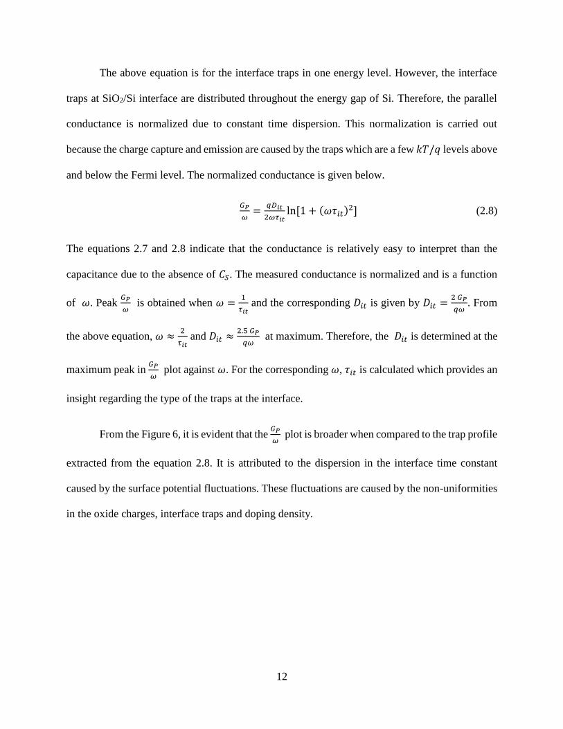
From the Figure 6, it is evident that the 𝐺𝑃
𝜔 plot is broader when compared to the trap profile
extracted from the equation 2.8. It is attributed to the dispersion in the interface time constant
caused by the surface potential fluctuations. These fluctuations are caused by the non-uniformities
in the oxide charges, interface traps and doping density.

13
Figure 6 : 𝐺𝑃
𝜔 v/s 𝜔 plot obtained from the equation 2.7 (single level) and 2.8 (continuum) and the
experimental data.
Therefore, surface potential fluctuations need to be accounted for the extraction of the trap profile.
In such cases, 𝐺𝑃
𝜔 is given by,
𝐺𝑃
𝜔= ∫
𝐷𝑖𝑡
𝜔𝜏𝑖𝑡ln [1 + (𝜔𝜏𝑖𝑡)2]𝑃(𝑈𝑆) 𝑑𝑈𝑆
∞
−∞ (2.9)
Where, 𝑃(𝑈𝑆) is the surface potential fluctuation probability distribution which is given by,
𝑃(𝑈𝑆) =1
√(2𝜋𝜎2)exp (−
(𝑈𝑆−�̅�𝑆)2
2𝜎2 ) (2.10)
Where, 𝜎 is the standard deviation whereas, �̅�𝑆 is the normalized mean surface potential.
Therefore, the expression for the 𝐷𝑖𝑡 as a function of 𝐺𝑃
𝜔 is given by
𝐷𝑖𝑡 ≈2.5
𝑞 (
𝐺𝑃
𝜔)
𝑚𝑎𝑥 (2.11)

14
The parallel conductance of a device is measured simultaneously with the parallel capacitance.
Therefore, assuming negligible series resistance, 𝐺𝑃
𝜔 can be calculated in terms of measured
capacitance 𝐶𝑚, measured conductance 𝐺𝑚 and the oxide capacitance 𝐶𝑜𝑥 which is given by
𝐺𝑃
𝜔=
𝜔𝐺𝑚𝐶𝑜𝑥2
𝐺𝑚2 +𝜔2(𝐶𝑜𝑥−𝐶𝑚)2 (2.12)
During the conductance measurements, the signal amplitude is kept at 50 mV or lower to
prevent harmonics. The presence of these harmonics in the signal frequency can give false
conductance values. One more noteworthy point would be that, for given 𝐷𝑖𝑡 the corresponding
conductance depends on the area of the device. For thin oxides, the series resistance will be
considered. So, now the circuit consists of tunnel conductance 𝐺𝑡 and series resistance 𝑟𝑠.
Therefore, 𝐺𝑃
𝜔 is given as
𝐺𝑃
𝜔=
𝜔(𝐺𝐶−𝐺𝑡)𝐶𝑜𝑥2
𝐺𝐶2+𝜔2(𝐶𝑜𝑥−𝐶𝐶)2 (2.13)
Where,
𝐶𝐶 =𝐶𝑚
(1−𝑟𝑠𝐺𝑚)2+(𝜔𝑟𝑠𝐶𝑚)2 (2.14)
𝐺𝐶 =𝜔2𝑟𝑠𝐶𝑚𝐶𝐶−𝐺𝑚
𝑟𝑠𝐺𝑚−1 (2.15)
where, 𝐶𝑚 and 𝐺𝑚 are the measured capacitance and conductance. The series resistance is obtained
by measuring the conductance and the capacitance in the accumulation region which is given by
𝑟𝑠 =𝐺𝑚𝑎
𝐺𝑚𝑎2 +𝜔2𝐶𝑚𝑎
2 (2.16)

15
where the 𝐺𝑚𝑎 and 𝐶𝑚𝑎 are the conductance and the capacitance measured in accumulation region.
To determine the tunnel conductance, equation 2.15 is considered as 𝜔 → 0, equation 2.13 is
reduced to equation 2.12, where 𝑟𝑠 = 𝐺𝑡 = 0.
2.3 Advantages of Conductance technique
The 𝐷𝑖𝑡 extracted by conductance technique is accurate when compared with the
capacitance methods. The complexity increases when the 𝐷𝑖𝑡 is extracted by the capacitance
methods because, the capacitance of a MOS-C consists of oxide capacitance, semiconductor
capacitance, depletion-layer capacitance and interface capacitance. Therefore, extracting the 𝐷𝑖𝑡
as a function of voltage and frequency through the capacitance measurements might give rise to
inaccuracies because the difference of the capacitance needs to be calculated. This is not the case
in the conductance technique, since the conductance is directly translatable to the response of the
interface traps as the function of voltage and frequency.
The conductance technique is capable of probing the 𝐷𝑖𝑡 of ~109 states/cm2-eV and lower
and entire band gap. This technique is capable of probing the interface traps in depletion and weak-
inversion region.
The 𝐷𝑖𝑡 is extracted based on the measured conductance of the MOS-C. No assumptions
are made to quantify the 𝐷𝑖𝑡. Also, no model is used to extrapolate the 𝐷𝑖𝑡 from the measured
capacitance of the MOS-C as in the case of Terman Method. It is because of these advantages that
we chose to use the conductance technique to analyze the interface states in MoS2-based FETs.
2.4 Literature on 𝑫𝒊𝒕 characterization of MoS2
Many different techniques have been used to extract 𝐷𝑖𝑡 for MoS2 based devices. Table 1
summarizes the 𝐷𝑖𝑡values obtained and the techniques used to extract the 𝐷𝑖𝑡.

16
Table 1: Dit values for MoS2-based devices reported in literature.
Device Structure Thickness Type of
MoS2
Method of Dit
Extraction
Dit Value
(states/cm2-
eV)
MoS2/ HfO2[12]
7-layer MoS2
13 nm HfO2 Exfoliated
High low
frequency
method and
multi-
frequency
1.2 × 10¹³
4-layer MoS2
8 nm HfO2
2×10¹¹ – 2 ×
1013
MoS2/ HfTiO[13]
50-layers (32.5 nm)
MoS2
39.65nm HfTiO
Transferred
by scotch
tape
From SS 5.58×10¹²
MoS2/ Al2O3[14]
1-layer (0.85 nm) MoS2
1nm Al2O3 seeding
layer
15 nm Al2O3 dielectric
CVD 1.6×10¹³
MoS2/h-BN[15] Single or bilayer MoS2
Exfoliated
by scotch
tape
observed noise
magnitude
6×10¹⁰ -
1×10¹²
MoS2/h-BN[16] Tri-layer MoS2 Exfoliated
High low
frequency
method and
multi-
frequency
~1012
MoS2/ZrO2[17] Few layers MoS2
5.8nm ZrO2 Transferred From SS 1.7×10¹²
MoS2/ HfO2[18]
Monolayer to tri-layer
(0.7nm to 2.1nm) MoS2
10nm HfO2
Exfoliated From SS 5×10¹²
MoS2/ Al2O3[19] 30nm MoS2
50nm Al2O3 Exfoliated From SS 2.6 × 10¹¹

17
Device Structure Thickness Type of
MoS2
Method of Dit
Extraction
Dit Value
(states/cm2-
eV)
MoS2/SiNx[20] 140-layers MoS2
250nm SiNx Exfoliated From SS 1.14×10¹³
MoS2/SiOx/SiNx
[20]
125-layers MoS2
50nm SiOx
200nm SiNx
Exfoliated From SS 2.13×10¹²
MoS2/thermal
SiO2[20]
154-layers MoS2
100 nm SiO2 Exfoliated From SS 3.32×10¹²
MoS2/Al2O3[21] 7 – 8 nm MoS2
10 nm Al2O3 Exfoliated Terman 1×10¹²
MoS2/HfO2[21] 7 – 8 nm MoS2
10 nm HfO2 Exfoliated Terman 2×10¹²
MoS2/HfO2[10]
Monolayer MoS2
5 nm HfO2 CVD
High-low
frequency
method
7.03×10¹¹
MoS2/Al2O3[22] 11.3 nm MoS2
30 nm Al2O3 Exfoliated
Low Frequency
Noise
characterization
1.8×10¹²
MoS2/Al2O3[23] 15nm MoS2
16nm Al2O3 Exfoliated
using CNF
Model 2.4×10¹²
2.5 Chapter Summary
In summary, we have discussed different techniques that can be employed to extract the
𝐷𝑖𝑡. Of all the techniques discussed, conductance technique is the most reliable method. Therefore,
we have employed this technique to extract 𝐷𝑖𝑡 at MoS2/h-BN and MoS2/Al2O3 devices. From the

18
overview of the different techniques employed to study the 𝐷𝑖𝑡 in the MoS2 based systems, it can
be understood that the conductance technique has not been employed yet to extract MoS2 𝐷𝑖𝑡.

19
CHAPTER 3: MoS2 FET DEVICE FABRICATION
In this chapter we discuss the structure of the MoS2 transistor adapted for the 𝐷𝑖𝑡 extraction.
We have fabricated MoS2 transistors with 2D h-BN as the gate dielectric to investigate a 2D/2D
interface. 2D/3D interfaces have also been fabricated using Al2O3 as the high- gate dielectric.
The specific steps in the device fabrication are outlined here.
3.1 Device Structure
For the 𝐷𝑖𝑡 extraction, the 2D channel considered is MoS2 and h-BN is the 2D dielectric
used. The 𝐷𝑖𝑡 is also extracted at MoS2 channel/ hi-k dielectric like Al2O3. To quantify the density
interface states in 2D channel/ dielectric interface, dual gated MoS2 Field Effect Transistor (FET)
is fabricated.
3.1.1 Device Schematic
The schematic of the MoS2 /h-BN FET is as shown in the Figure 7. The top gate contact is
patterned such that there are underlapped regions near the source and drain. These regions are kept
populated with electrons using the back gate voltage, so that series resistance can be minimized
during capacitance and conductance measurements. The optical microscope image of the MoS2/h-
BN device is shown Figure 8.

20
Figure 7 : Device schematic of MoS2/h-BN FET.
Figure 8 : Optical microscope image of MoS2/h-BN device.
3.1.2 Scanning Electron Microscopy (SEM) of MoS2 FET
The SEM image of the complete device is shown in the Figure 9. The SEM was performed
with Zeiss Ultra 55 SEM.

21
Figure 9 : SEM image of the MoS2/h-BN device.
3.1.3 Transmission Electron Microscopy (TEM) of MoS2 FET
To confirm the quality of layer stacking, cross-sectional transmission electron microscopy
(TEM) is performed on a representative device with monolayer MoS2 as the channel. Initially, a
cross-section sample was lifted off using Helios Nanolab 600 Dual Beam Focused Ion Beam
Milling System followed by the TEM characterization using JEOL 2010F operated at 200 kV
acceleration voltage. Figure 10 shows the cross-sectional TEM micrograph of the MoS2/h-BN
layer stacked on SiO2 substrate followed by Nickel top gate. Monolayer MoS2 can be clearly seen
on the SiO2 substrate. Multilayer structure stacked on the MoS2 layer had a interlayer spacing of
~0.34 nm corresponding to h-BN, and the van der Waals interface between MoS2 and h-BN was
clean, highly coherent and free of any structural disorders.

22
Figure 10 : cross sectional TEM of a representative monolayer MoS2 FET with h-BN dielectric.
(Courtesy: Supriya Koul and Professor Akihiro Kushima, UCF)
3.2 Fabrication procedure
The MoS2 FETs are fabricated using multiple lithography processes. E-beam lithography
is used to fabricate dual gated MoS2 FETs.
3.2.1 Alignment marks patterning using photolithography
The starting substrate for the device fabrication is 260 nm thermally grown SiO2 on p+ Si
wafers.. The device fabrication starts with the alignment marks patterning using conventional
photolithography on the SiO2/Si substrate. These marks are used to locate 2-7 nm thick MoS2
flakes, and are used during e-beam lithography for the alignment. The patterning is carried out
with positive resist S1813 from Microposit. The resist is spin-coated at a speed of 4500 rpm with
an acceleration of 300 rpm/sec for 1 minute. The soft-baking is carried out for spin-coating for 1
min at 115 ºC. MJB 4 Karl Suss Aligner is used for the alignment and exposure. The exposure
dose is 10.21 mJ/cm2 and the exposure is done for 9 s. After the exposure, the patterns are
developed in CD-26 resist developer for 35 s.

23
3.2.2 Mechanical Exfoliation of MoS2 flakes
The device fabricated consists of MoS2 flake (SPI supplies) 3-10 layers thick as the channel
material. The MoS2 flake is isolated by mechanical exfoliation using Scotch-tape method where
few layers of MoS2 are cleaved from the bulk MoS2 using scotch tape and then transferred on the
patterned Si/SiO2 substrate. After the exfoliation, the flakes of desired thickness are located on the
substrate.
3.2.3 Back-gated MoS2 FET fabrication
The patterning of the device is carried out by e-Beam lithography. This lithography
procedure requires the mask design for individual flakes. The sample is spin-coated with
MicroChem 950 PMMA C4 e-beam resist (positive). The spin coating is done at 2 different speeds.
At first, the resist is spun at 500 rpm for 30 s followed by 4000 rpm for 30 s. The sample is then
soft-baked at 130 °C for 3 mins. The e-beam lithography is carried out using Zeiss Ultra 55
scanning electron microscope (SEM) integrated with Nanometer Pattern Generation System
(NPGS). The contact fingers are smaller and are written at a current ~ 100 nA with a dose of 350
µC/cm2 while the contact pads which are larger are written with a current of ~1.4 nA and the similar
dose as before. Then, the development is done by immersing the sample in a mixture of MIBK:
IPA in the ratio of 1:3 for 45 seconds followed by an IPA bath for 1 min.
The evaporation is carried out after the patterning for the lift-off of the metal. The e-beam
evaporation is carried out in Thermionics system. 30 nm of Nickel is deposited at a pressure of 4
× 10-6 Torr as the contact metal. After the deposition, lift-off is carried out by immersing the sample
in the Acetone bath at 60 °C for 25 mins. This completes the fabrication of back-gated MoS2 FET.
24
3.2.4 Top-gated MoS2 FET fabrication
3.2.4.1 Dielectric deposition by dry transfer of h-BN flakes
The top-gated FET fabrication procedure is explained as follows. For the fabrication of the
MoS2 FET with h-BN top gate dielectric, a dry transfer technique is used. For the dry transfer of
h-BN, mechanical exfoliation of h-BN using scotch tape is carried out on the visco-elastic stamp.
Followed by this, mapping of h-BN flakes of thickness ~13 nm is carried out. After this, the h-BN
flakes are transferred on the MoS2 channel. Then, the top gate contact is patterned using e-beam
lithography and 30 nm Ni is deposited as the contact metal followed by lift-off in an acetone bath.
This marks the end of the MoS2/ h-BN device fabrication.
3.2.4.2 Dielectric deposition by Atomic Layer Deposition (ALD)
Due to the absence of dangling bonds, the deposition of dielectrics by Atomic Layer
Deposition (ALD) is not uniform. Therefore, nucleation layer is deposited prior to ALD for
functionalizing the top surface of MoS2.[24-26] This nucleation layer aides for the uniform
deposition of the dielectric. Two different nucleation layers, such as AlOx and SiOx of 1.5 nm
thickness are deposited.
For the seeding layer deposition, 1.5 nm Al and SiOx is e-beam evaporated and left to
oxidize in air for a few minutes. The stoichiometric composition of the oxide layer formed is AlOx
and SiOx. Followed by this, ALD (Cambridge Nanotech) is carried out. 8.5 nm thick Al2O3 is
deposited at 250 °C at 85 mTorr using Trimethylaluminium (TMA) and H2O precursors. After the
dielectric deposition, the top-gate is patterned by e-beam lithography and 30 nm Ni e-beam
evaporated as the contact metal, followed by lift-off.

25
3.3 Chapter Summary
Dual gated MoS2 FETs are fabricated. 3 types of devices were fabricated for the Dit
extraction. Devices with Al2O3 gate dielectric were fabricated using AlOx and SiOx seeding layer.
MoS2 FETs with h-BN gate dielectric were also fabricated.

26
CHAPTER 4: EXPERIMENTAL RESULTS
In this chapter, we report the capacitance-voltage and conductance-voltage characteristics
of the fabricated devices. We extract the interface trap densities using the conductance method for
the MoS2 FETs. Initially, the 𝐷𝑖𝑡 was extracted for the pristine devices and is followed by the
studies of effect of forming gas annealing on the 𝐷𝑖𝑡.
4.1 Pristine device characteristics
Before the dielectric deposition and further processing, the characteristics of the back-gated
MoS2 FET is tested to investigate the conductivity of the MoS2 flake because the micro-tears
between the electrodes will cause the open circuit restricting the flow of the current. The back-
gated current-voltage (I-V) characteristics of a representative MoS2 FET shown in the Figure 11.
Figure 11 : Back-gated I-V of MoS2 FET. Inset: The device on which the back-gated I-V
characterization was performed.
4.1.1 Current-Voltage (I-V) Characteristics
After the completion of fabrication of the top-gated devices, the electrical measurements
were performed on the devices. At first the top-gated I-V is carried out. For this measurement, the

27
bias is applied on the top-gate by keeping the back-gate at 0 V. Figures 12, 13 and 14 show the
transfer characteristics of the FETs with AlOx/Al2O3, SiOx/Al2O3 and h-BN top gate dielectrics,
respectively at 𝑉𝐷 = 50 𝑚𝑉 & 1 𝑉. The subthreshold swing (SS) is calculated from the I-V
characteristics. The SS of the MoS2 FET with AlOx/Al2O3 gate dielectric is 160 mV/decade (Figure
12), with SiOx/ Al2O3 gate dielectric is 180 mV/decade (Figure 13) while the SS of the device
with h-BN gate dielectric is 140 mV/decade (Figure 14).
Figure 12 : Transfer characteristics of top-gated MoS2 /Al2O3 device with AlOx seeding layer.

28
Figure 13 : Top-gated transfer characteristics of MoS2 /Al2O3 device with SiOx seeding layer.
Figure 14 : Top-gated transfer characteristics of MoS2 FET with h-BN dielectric.

29
After the I-V characterization, Capacitance-Voltage (C-V) measurements are carried out.
For these measurements, we shorted the source and drain and connected them to the ‘low’ terminal
of the capacitance measurement unit (CMU). We modified the bias on the ‘high’ terminal of the
capacitance measurement unit that was connected to the top gate electrode. The back gate was
grounded at 0 V. Since in our depletion mode MoS2 FET, the channel is quite populated with
electrons at VBG = 0 V, keeping the underlapped channel regions conductive.
4.1.2 C-V and G-V characteristics
Figure 15 shows the equivalent circuit model of the capacitances and resistances that come
into play while measuring the capacitance between the gate electrode and the source/drain
electrodes. The MoS2 FET consists of various capacitances semiconductor capacitance 𝐶𝑏𝑜𝑑𝑦,
interface capacitance 𝐶𝑖𝑡 and oxide capacitance 𝐶𝐺 represented by 𝐶𝑚 and corresponding
conductance 𝐺𝑚.
Figure 15 : Capacitance model for the MoS2 FET.
Before, the measurements the CMU is calibrated first. The CMU is first open calibrated by
keeping all the terminals open. Followed by this, the short calibration is performed by connecting

30
the top-gate terminal and the common source and drain terminal on a metal bar. The calibration is
performed for the frequencies ranging between 1 kHz to 5 MHz. After this, the C-V program is
executed in open circuit to make sure the RMS value of the capacitance as measured by the CMU
is ~0 F. The device is always swept from accumulation to depletion region for multiple discrete
frequencies viz.,1 kHz, 5 kHz, 10 kHz, 20 kHz, 50 kHz, 100 kHz and 200 kHz. The gate voltage
is superimposed with an ac signal of amplitude 50 mV. The measurements were done with high
integration factor (slow) which allows the interface traps to respond to the applied bias. The C-V
characteristics of the pristine MoS2/Al2O3 devices with AlOx and SiOx, and the MoS2/h-BN device
are shown in the Figures 16, 17 and 18 respectively.
Figure 16 : C-V plots for pristine MoS2 FET with AlOx/Al2O3 gate dielectric.

31
Figure 17 : C-V plots for pristine MoS2 FET with SiOx/Al2O3 gate dielectric.
As observed from the plots the dispersion in the depletion region is a clear signature of the
interface trap response to the applied gate bias. The high capacitance in the accumulation region
is attributed to the parasitic capacitances because of the un-gated region adjacent to source and
drain. The Al2O3 device with AlOx seeding layer show more dispersion in comparison with other
two devices indicating that AlOx seeding layer has more traps.

32
Figure 18 : Pristine C-V plots for h-BN dielectric device.
The conductance-voltage (G-V) characteristics are shown in the Figures 19, 20 and 21 for
AlOx/Al2O3, SiOx/Al2O3 and h-BN gated devices respectively. The conductance variation as a
function of frequency is observed. Distinct increase in the peak is observed with the increase in
frequency. Also, the device with AlOx seeding layer shows the maximum conductance of 53 nS at
200 kHz when compared to SiOx and h-BN device at the same frequency.
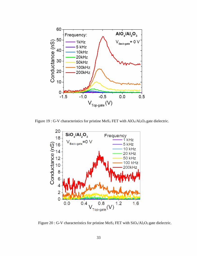
33
Figure 19 : G-V characteristics for pristine MoS2 FET with AlOx/Al2O3 gate dielectric.
Figure 20 : G-V characteristics for pristine MoS2 FET with SiOx/Al2O3 gate dielectric.

34
Figure 21 : G-V characteristics for pristine MoS2 FET with h-BN gate dielectric.
After the C-V measurements, the capacitance and conductance are measured at a constant
voltage bias as a function of frequency. Now the conductance technique is implemented to extract
the 𝐷𝑖𝑡.
4.1.3 Dit extraction for pristine devices using the conductance technique
The conductance method was implemented at room temperature in air. The corrected
capacitance Cc and conductance Gc need to be extracted first since the device possesses series
resistances from the ungated regions and from the contacts. The series resistance is obtained by
biasing the device in accumulation, and then the following expression is applied:
𝑅𝑆 =𝐺𝑚𝑎
𝐺𝑚𝑎2 +𝜔2𝐶𝑚𝑎
2 (4.1)
35
Gma and Cma are the measured conductance and capacitance, respectively, in the accumulation
region, = 2 frequency. Followed by this, the series resistance factor denoted by 𝑎 is calculated
as 𝑎 = 𝐺𝑚 − (𝐺𝑚2 + 𝜔2𝐶𝑚
2 )𝑅𝑆, where Gm and Cm are the measured conductance and capacitance,
respectively. Gc and Cc can be then calculated as:
𝐺𝐶 =(𝐺𝑚
2 +𝜔2𝐶𝑚2 )𝑎
𝑎2+𝜔2𝐶𝑚2 (4.2)
𝐶𝐶 =(𝐺𝑚
2 +𝜔2𝐶𝑚2 )𝐶𝑚
𝑎2+𝜔2𝐶𝑚2 (4.3)
Now Gp/ can be calculated as follows:
𝐺𝑝
𝜔=
𝜔𝐺𝐶𝐶𝐺2
𝐺𝐶2+𝜔2(𝐶𝐺−𝐶𝐶)2 (4.4)
Here, Gp is the equivalent parallel capacitance, CG is the gate capacitance, which not only involves
the gate dielectric capacitance, but also the quantum capacitance of MoS2. We take CG as the
capacitance in the accumulation region of the C-V curves.
Finally, Dit is calculated as: 𝐷𝑖𝑡 =2.5
𝑞
𝐺𝑝
𝜔 at the maximum.
Figures 22, 23 and 24 shows the G/–f curves for gate voltages varied from depletion to
accumulation in pristine MoS2 FETs with AlOx/Al2O3, SiOx/Al2O3 gate dielectric and h-BN gate
dielectric respectively. As observed from the plots, G/ peak positions are voltage dependent,
which clearly indicates that the Fermi level is unpinned. This confirms that the conductance
method can be used to determine the interface trap density.[27] In certain cases of III-V/hi-
interfaces, the Fermi level is pinned and the conductance peak does not change with the gate
voltage applied, causing the conductance method to be inapplicable there.[27] At flat band
condition, the Fermi level is close to the conduction band edge. Any voltage applied below the flat

36
band condition directly translates to how much the Fermi level moves into the bandgap. From
Figures 22 and 23 it can be inferred that for Al2O3 gate dielectric, the peak is observed to shift
towards right as the Fermi level moves further into the band gap while the h-BN dielectric device
in Figure 24 exhibits the left shift in the maximum peak.
Figure 22 : G/–f curves for gate voltages varied from depletion to accumulation for pristine
MoS2 FET with AlOx seeding layer.
37
Figure 23 : G/–f curves for gate voltages varied from depletion to accumulation for pristine
device with SiOx seeding layer.
Figure 24 : G/–f curves for gate voltages varied from depletion to accumulation for pristine h-
BN device.

38
Figure 25 : Dit v/s trap position for the pristine Al2O3 and h-BN devices.
The extracted Dit values as a function of the trap position (ET–Ec) for the Al2O3 and h-BN
gated devices as shown in the Figure 25. At midgap, the Dit extracted for pristine AlOx/Al2O3
device is ~ 1.11012 states/cm2-eV and is nearly constant through the band-gap. Whereas, the
pristine SiOx/Al2O3 gate dielectric exhibited the 𝐷𝑖𝑡 of 5.91011 states/cm2-eV near the conduction
band edge and 1.61011 states/cm2-eV near the valence band edge. From this it can be inferred that
the device with SiOx seeding layer exhibits lower 𝐷𝑖𝑡 when compared with the AlOx seeding layer
device. For a 2D h-BN dielectric device, it is seen that the 𝐷𝑖𝑡 is 41011 states/cm2-eV near the
valence band edge which is relatively higher than the Dit near conduction band edge which is
21011 states/cm2-eV. While the Dit profile looks slightly different for the device with h-BN
dielectric, the Dit values are similar to the case with SiOx/Al2O3, the midgap Dit is lower 1011
states/cm2-eV. The AlOx/Al2O3 devices exhibit the mid-gap Dit of 1.51012 states/cm2-eV.

39
Figure 26 : Trap time constants v/s trap position for the pristine Al2O3 and h-BN devices.
The trap time constants are also plotted in Figure 26 and the interface trap time constants
can be obtained from the relation: 𝜏𝑖𝑡 = 2 𝜔⁄ , where 𝜔 is the radial frequency corresponding to
the peak of the 𝐺/𝜔 vs. f curve.[11] The interface trap time constants for the MoS2/SiOx/Al2O3 and
MoS2/h-BN interfaces are similar, signifying that similar defects contribute to the interface traps
in these devices. The identity of defects in MoS2 causing interface trap formation is debatable.
Several reports indicate that the interface traps in MoS2 based FETs originate from the sulfur
vacancies in MoS2.[28, 29]
4.2 Effect of forming gas annealing
Since the AlOx/Al2O3 device exhibited relatively higher midgap Dit of 1.51012 states/cm2-
eV compared to SiOx and h-BN devices, further studies were conducted on the latter types with

40
low Dit values. Forming gas annealing is known to reduce Dit in silicon-based devices. This is why
we subjected the SiOx/Al2O3 and h-BN gated devices to forming gas annealing (FGA) to study its
effect on Dit. The devices were annealed in forming gas composed of 10% H2, 90% N2. The MoS2/
h-BN devices were annealed at 250 ºC for 2 h with the ramp time of 30 mins. The MoS2/Al2O3
devices were annealed for 30 mins at 120 ºC. A lower annealing temperature and duration was
chosen for the Al2O3-gated devices since they showed increased gate leakage for higher annealing
temperatures and durations.
4.2.1 I-V Characteristics post FGA
After annealing, the devices were tested for transfer characteristics shown in the Figure 27
and we saw the substantial decrease in the SS indicating that the defects are passivated by forming
gas. The SS of the h-BN device decreased from 140 mV/decade to 100 mV/decade. The SS of
SiOx/Al2O3 decreased from 160 mV/decade to 95 mV/decade.
Figure 27 : Post FGA transfer characteristics for MoS2 FET with Al2O3 gate dielectric with SiOx
seeding layer. Inset: Transfer characteristics for MoS2/h-BN device.

41
Dit is extracted analytically from the SS, using circuit models. The following analytical
expression is used to extract Dit,[30, 31]
𝑆𝑆 =2.3𝑘𝑇
𝑞(1 +
𝐶𝑖𝑡
𝐶𝑡𝑔+
𝐶𝑏𝑜𝑑𝑦
𝐶𝑡𝑔−
𝐶𝑏𝑜𝑑𝑦2
𝐶𝑡𝑔𝐶𝑆𝑖𝑂2
1+𝐶𝑖𝑡
𝐶𝑆𝑖𝑂2+
𝐶𝑏𝑜𝑑𝑦
𝐶𝑆𝑖𝑂2
) (4.5)
Here, Cit is the interface trap capacitance. Ctg is the capacitance of the top gate dielectric, given by
𝐶𝑡𝑔 = 𝜖𝑡𝑔 𝑡𝑡𝑔⁄ , where 𝜖𝑡𝑔is the dielectric constant and 𝑡𝑡𝑔 is the thickness of the top gate dielectric.
For h-BN, Ctg = 0.204 F/cm2, assuming 𝜖ℎ−𝐵𝑁 = 3,[32] and the thickness of the h-BN flake, th-BN
is measured by atomic force microscopy to be 13 nm. For Al2O3, Ctg = 0.387 F/cm2, considering
the gate dielectric stack thickness 𝑡𝐴𝑙2𝑂3 = 9.5 nm and a nucleation layer 𝑡𝑆𝑖𝑂𝑥
= 1.5 nm, with 𝜖𝐴𝑙2𝑂3
= 5 (experimental) and assuming 𝜖𝑆𝑖𝑂𝑥 =3.9. 𝐶𝑆𝑖𝑂2
= 𝜖𝑆𝑖𝑂2𝑡𝑆𝑖𝑂2
⁄ =0.013 F/cm2, given 𝜖𝑆𝑖𝑂2= 3.9,
and the thickness of SiO2 is 260 nm. 𝐶𝑏𝑜𝑑𝑦 = 𝐶𝑀𝑜𝑆2= 𝜖𝑀𝑜𝑆2
𝑡𝑀𝑜𝑆2⁄ = 1.26 F/cm2, using 𝜖𝑀𝑜𝑆2
=
4,[33] and thickness of 4-layer MoS2 flake is 2.8 nm. For the h-BN device with SS = 100 mV/dec,
a Dit of 41011 states/cm2-eV is extracted using equation (4.5). Similarly, for Al2O3 device with
SS = 95 mV/dec, a Dit of 61011 states/cm2-eV is extracted. The interface trap densities thus
obtained are impressive and are comparable with the highest quality of Si/high- dielectric
interfaces.[34-36] Thus, our MoS2/h-BN and MoS2/SiOx/Al2O3 interfaces can yield high quality,
low-Dit interfaces after only a mild forming gas annealing.
4.2.2 Post FGA C-V and G-V characteristics
The capacitance and conductance of the top-gated MoS2 FETs were examined next.
Figures 28 and 29 show the capacitance-voltage and conductance-voltage characteristics as a
function of frequency for SiOx/Al2O3 and h-BN top-gated device, respectively. Both the C-V
curves do not show any significant frequency dependence in the depletion region from 1 kHz to

42
500 kHz, indicating the presence of few interface traps. The absence of sharp peaks in the parallel
conductance vs. top gate voltage curves are also indicative of low Dit.[37, 38] The high capacitance
in the accumulation region is attributed to parasitic capacitances due to the ungated regions
adjacent to the source and drain. The frequency dispersion in the accumulation region for the
SiOx/Al2O3 gated device is attributed to border traps.[10, 39] It is worth noting that the h-BN-gated
device does not show frequency dispersion in the accumulation region, indicating a lower density
of border traps in h-BN compared to SiOx/Al2O3. The dispersion in the depletion and deep
depletion regions are due to the interface traps.
Figure 28 : Post FGA C-V and G-V characteristics of SiOx/Al2O3 device showing relatively
reduced frequency dispersion in the depletion region

43
Figure 29 : Post FGA C-V and G-V characteristics of h-BN device showing relatively reduced
frequency dispersion in the depletion region
4.2.3 Post FGA Dit extraction by conductance method
Figure 30 shows the G/–f curves for gate voltages varied from depletion to accumulation
in an MoS2 FET with SiOx/Al2O3 gate dielectric and h-BN gate dielectric. Figure 30 shows the
extracted Dit values and interface trap time constants as a function of the trap position (ET–Ec) for
the SiOx/Al2O3 and h-BN gated devices.

44
Figure 30 : Post FGA G/–f curves for gate voltages varied from depletion to accumulation in an
MoS2 FET with SiOx/Al2O3 gate dielectric and h-BN gate dielectric.
For the device with SiOx/Al2O3 gate dielectric, the G/ peak increases as the gate voltage
is swept from flat band to depletion, indicating the increase in Dit as the Fermi level shifts further
into the band gap from the conduction band edge. An opposite trend is observed below the midgap.
In case of the device with h-BN gate dielectric, the G/ peak gets reduced from flat band to
depletion.

45
Figure 31 : Post FGA Dit v/s trap position exhibiting the decrease in the Dit for the SiOx/Al2O3
and h-BN devices.
The post FGA Dit and 𝜏𝑖𝑡profiles of SiOx/Al2O3 and h-BN devices are shown in the Figure
31. At midgap, the Dit extracted for SiOx/Al2O3 gate dielectric is ~1.31011 states/cm2-eV, while
the Dit is 91010 states/cm2-eV near the conduction band edge, and the Dit is 71010 states/cm2-eV
near the valence band edge. While the Dit profile looks slightly different for the device with h-BN
dielectric, the Dit values are similiar to the case with SiOx/Al2O3, with a midgap Dit for this 2D/2D
interface being ~71010 states/cm2-eV. At least two devices of each type showed similar
characteristics. The low value of Dit obtained for MoS2/h-BN interface is due to the absence of
dangling bonds at 2D/2D interface. In our device structure, the MoS2 layers are encapsulated by
the h-BN top gate, leaving no free surfaces for increased trap states. Dit for monolayer and tri-layer
MoS2 with h-BN underneath MoS2 was extracted by Chen et al., to be in the range of 10 states/cm2-
eV, despite the capacitance-voltage characteristics showing no frequency dispersion. We believe

46
that the implementation of the conductance method helps us in extracting the low Dit values from
these MoS2/h-BN systems accurately. It is well-known that the inclusion of a nucleation layer
increases the interface traps. However, our experiments show that the interface quality of a
2D/high- system where SiOx is used as the nucleation layer for ALD of Al2O3 exhibits Dit values
close to the 2D/2D dangling-bond-free interface enabled by h-BN on MoS2. The observation of
low Dit values using SiOx nucleation layer could be due to its ability to facilitate faster reactions
between surface hydroxyl groups and ALD precursors.[40] The Dit values we obtained from the
SS analysis are in the ballpark of the Dit values extracted using the conductance method. The low
Dit clearly establishes the superior quality of 2D/2D van der Waals interface and 2D/high-
interfaces for realizing high performance and reliable (opto)electronic devices. The interface trap
time constants can be obtained from the relation: 𝜏𝑖𝑡 = 2 𝜔⁄ , where 𝜔 is the radial frequency
corresponding to the peak of the 𝐺/𝜔 vs. f curve. The interface trap time constants for the
MoS2/SiOx/Al2O3 and MoS2/h-BN interfaces are similar, signifying that similar defects contribute
to the interface traps in these devices. The identity of defects in MoS2 causing interface trap
formation is debatable.[41] Several reports indicate that the interface traps in MoS2 based FETs
originate from the sulfur vacancies in MoS2.[10]
4.3 Chapter Summary
In summary, we report high-quality interfaces in a semiconductor system, enabled by
2D/2D and 2D/high--dielectric systems. Using the conductance method, a midgap interface trap
density as low as 71010 states/cm2-eV can be obtained by MoS2/h-BN device. The 𝐷𝑖𝑡 varies from
71010 to 1011 states/cm2-eV at an MoS2/Al2O3 interface if SiOx is used as the nucleation layer.

47
CHAPTER 5: CONCLUSION
This thesis investigates the interfaces properties of MoS2 with top gate dielectrics, such as
2D h-BN and Al2O3 high- dielectric. The ALD of Al2O3 was enabled by the deposition of AlOx
and SiOx as the nucleation layers. The 𝐷𝑖𝑡 is probed and quantified using one of the most reliable
methods – the conductance technique. From this study, we observe that 2D MoS2 with 2D
dielectric h-BN and hi-k dielectric Al2O3 enables a high quality semiconductor system. We also
report the effect of seeding layer on the 𝐷𝑖𝑡. From the extracted 𝐷𝑖𝑡, it is observed that using AlOx
seeding layer introduces a 𝐷𝑖𝑡 of 11012 states/cm2-eV, whereas the 𝐷𝑖𝑡 of the interface with SiOx
seeding layer 71010 to 1011 states/cm2-eV comparable with the midgap 𝐷𝑖𝑡 of 71010 states/cm2-
eV extracted from MoS2/h-BN after mild forming gas annealing. This clearly indicates that the
layered materials result in high-quality interfaces with both 2D dielectric and hi-k dielectric,
reinforcing their potential as channel material for various high performance and reliable electronics
and optoelectronics.
5.1 Future Scope
This thesis emphasizes on quantifying the density of interface traps using the conductance
technique. However, the origin of interface states is believed to be the inherent defects present in
the material. Therefore, a more comprehensive study is required to shed the light on the genesis of
the traps at 2D/2D interface. Also, a detailed study is required for regarding the decrease in the
interface traps with SiOx seeding layer. The locations of the interface traps extracted by the
conductance technique needs to be accurately determined using modeling of the MoS2 bandgap.
The effect of border traps needs to be quantified and compared with the effect of interface traps.
The Dit needs to be extracted using other techniques mentioned in Chapter 2, and a comparison
needs to be made of the efficiency of these techniques.

48
REFERENCES
1. Ferain, I., C.A. Colinge, and J.-P. Colinge, Multigate transistors as the future of classical
metal–oxide–semiconductor field-effect transistors. Nature, 2011. 479(7373): p. 310.
2. Dean, C.R., et al., Boron nitride substrates for high-quality graphene electronics. Nature
nanotechnology, 2010. 5(10): p. 722.
3. Jariwala, D., et al., Carbon nanomaterials for electronics, optoelectronics, photovoltaics,
and sensing. Chemical Society Reviews, 2013. 42(7): p. 2824-2860.
4. Zappa, D., Molybdenum Dichalcogenides for Environmental Chemical Sensing. Materials,
2017. 10(12): p. 1418.
5. Frindt, R., Single crystals of MoS2 several molecular layers thick. Journal of Applied
Physics, 1966. 37(4): p. 1928-1929.
6. Joensen, P., R. Frindt, and S.R. Morrison, Single-layer MoS2. Materials research bulletin,
1986. 21(4): p. 457-461.
7. Chhowalla, M., D. Jena, and H. Zhang, Two-dimensional semiconductors for transistors.
Nature Reviews Materials, 2016. 1(11): p. 16052.
8. Sze, S.M., Physics of Semiconductor Devices. 1981: John Wiley & Sons.
9. Addou, R., L. Colombo, and R.M. Wallace, Surface defects on natural MoS2. ACS applied
materials & interfaces, 2015. 7(22): p. 11921-11929.
10. Xia, P., et al., Impact and origin of interface states in MOS capacitor with monolayer MoS
2 and HfO 2 high-k dielectric. Scientific reports, 2017. 7: p. 40669.
11. Schroder, D.K., Semiconductor material and device characterization. 2006: John Wiley &
Sons.
12. Zhao, P., et al., Probing Interface Defects in Top-Gated MoS2 Transistors with Impedance
Spectroscopy. ACS applied materials & interfaces, 2017. 9(28): p. 24348-24356.
13. Wen, M., et al., Improved Electrical Performance of Multilayer MoS 2 Transistor With NH
3-Annealed ALD HfTiO Gate Dielectric. IEEE Transactions on Electron Devices, 2017.
64(3): p. 1020-1025.
14. Liu, H., et al., Statistical study of deep submicron dual-gated field-effect transistors on
monolayer chemical vapor deposition molybdenum disulfide films. Nano letters, 2013.
13(6): p. 2640-2646.

49
15. Ghatak, S., et al., Microscopic origin of low frequency noise in MoS2 field-effect
transistors. APL Materials, 2014. 2(9): p. 092515.
16. Chen, X., et al., Probing the electron states and metal-insulator transition mechanisms in
molybdenum disulphide vertical heterostructures. Nature communications, 2015. 6: p.
6088.
17. Desai, S.B., et al., MoS2 transistors with 1-nanometer gate lengths. Science, 2016.
354(6308): p. 99-102.
18. Wang, J., et al., Integration of High‐k Oxide on MoS2 by Using Ozone Pretreatment for
High‐Performance MoS2 Top‐Gated Transistor with Thickness‐Dependent Carrier
Scattering Investigation. small, 2015. 11(44): p. 5932-5938.
19. Kim, S., et al., JY; Choi, YW Jin, SY Lee, D. Jena, W. Choi and K. Kim. Nat. Commun,
2012. 3: p. 1011.
20. Lee, C.-H., N. Vardy, and W.S. Wong, Multilayer MoS 2 thin-film transistors employing
silicon nitride and silicon oxide dielectric layers. IEEE Electron Device Letters, 2016.
37(6): p. 731-734.
21. Takenaka, M., et al. Quantitative evaluation of energy distribution of interface trap density
at MoS 2 MOS interfaces by the Terman method. in Electron Devices Meeting (IEDM),
2016 IEEE International. 2016. IEEE.
22. Na, J., et al., Low-frequency noise in multilayer MoS 2 field-effect transistors: the effect of
high-k passivation. Nanoscale, 2014. 6(1): p. 433-441.
23. Liu, H. and D.Y. Peide, $\hbox {MoS} _ {2} $ Dual-Gate MOSFET With Atomic-Layer-
Deposited $\hbox {Al} _ {2}\hbox {O} _ {3} $ as Top-Gate Dielectric. IEEE electron device
letters, 2012. 33(4): p. 546-548.
24. Kim, S., et al., Realization of a high mobility dual-gated graphene field-effect transistor
with Al 2 O 3 dielectric. Applied Physics Letters, 2009. 94(6): p. 062107.
25. Roy, T., et al., Dual-gated MoS2/WSe2 van der Waals tunnel diodes and transistors. Acs
Nano, 2015. 9(2): p. 2071-2079.
26. Tosun, M., et al., High-gain inverters based on WSe2 complementary field-effect
transistors. ACS nano, 2014. 8(5): p. 4948-4953.

50
27. Engel-Herbert, R., Y. Hwang, and S. Stemmer, Comparison of methods to quantify
interface trap densities at dielectric/III-V semiconductor interfaces. Journal of applied
physics, 2010. 108(12): p. 124101.
28. Qiu, H., et al., Hopping transport through defect-induced localized states in molybdenum
disulphide. Nature communications, 2013. 4: p. 2642.
29. Cho, K., et al., Electrical and optical characterization of MoS2 with sulfur vacancy
passivation by treatment with alkanethiol molecules. ACS nano, 2015. 9(8): p. 8044-8053.
30. Colinge, J.-P., D. Flandre, and F. Van de Wiele, Subthreshold slope of long-channel,
accumulation-mode p-channel SOI MOSFETs. Solid-state electronics, 1994. 37(2): p. 289-
294.
31. Wouters, D.J., J.-P. Colinge, and H.E. Maes, Subthreshold slope in thin-film SOI
MOSFETs. IEEE Transactions on Electron Devices, 1990. 37(9): p. 2022-2033.
32. Kim, K.K., et al., Synthesis and characterization of hexagonal boron nitride film as a
dielectric layer for graphene devices. ACS nano, 2012. 6(10): p. 8583-8590.
33. Santos, E.J. and E. Kaxiras, Electrically driven tuning of the dielectric constant in MoS2
layers. ACS nano, 2013. 7(12): p. 10741-10746.
34. Balog, M., et al., Chemical vapor deposition and characterization of HfO2 films from
organo-hafnium compounds. Thin Solid Films, 1977. 41(3): p. 247-259.
35. Balog, M., et al., Thin films of metal oxides on silicon by chemical vapor deposition with
organometallic compounds. I. Journal of Crystal Growth, 1972. 17: p. 298-301.
36. Shappir, J., A. Anis, and I. Pinsky, Investigation of MOS capacitors with thin ZrO 2 layers
and various gate materials for advanced DRAM applications. IEEE Transactions on
Electron Devices, 1986. 33(4): p. 442-449.
37. Krieger, M., et al., Analysis of interface trap parameters from double‐peak conductance
spectra taken on N‐implanted 3C‐SiC MOS capacitors. physica status solidi (b), 2008.
245(7): p. 1390-1395.
38. Zvara, M., et al., Interface trap conductance spectroscopy of a narrow-gap Hg1-xCdxTe
(x approximately= 0.2) MIS device. Semiconductor science and technology, 1995. 10(8):
p. 1145.
39. Zhao, P., et al., Evaluation of border traps and interface traps in HfO2/MoS2 gate stacks
by capacitance–voltage analysis. 2D Materials, 2018. 5(3): p. 031002.

51
40. Zhang, H., et al., MoS2 Functionalization with a Sub-nm Thin SiO2 Layer for Atomic Layer
Deposition of High-κ Dielectrics. Chemistry of Materials, 2017. 29(16): p. 6772-6780.
41. Hong, J., et al., Exploring atomic defects in molybdenum disulphide monolayers. Nature
communications, 2015. 6: p. 6293.


![2D MoS2 Layer-Dependent Dielectric ...nom.mse.hust.edu.cn/pdf/2019_ADV_OPT_MATER.pdf · of the 2D MoS 2 with the help of theoretical calculations.[31,32] For example, Johari et al.](https://static.fdocuments.net/doc/165x107/5ffa2952d0ea6060614ae938/2d-mos2-layer-dependent-dielectric-nommsehusteducnpdf2019advoptmaterpdf.jpg)


