Status of ATF Collaboration The unique test facility for ILC with a low emittance beam.
Upload
avariella-kingCategory
view
25download
0description

CCAST@Beijing 1
High Polarization and Low Emittance Electron Source
for ILC
Nagoya UniversityDept. of Physics (SP-Lab)
Masahiro Yamamoto

CCAST@Beijing 2
Nagoya UniversityT.Nakanishi, S.Okumi, M.Yamamoto, N.Yamamoto,A.Mano, Y.Nakagawa, T.Konomi
T.Ujihara, T.Katoh, X.G.Jin, M.Tanioku, Y.Takeda
Hiroshima UniversityM.Kuriki
Osaka Prefecture UniversityH. Horinaka, T. Matsuyama
KEKF.Furuta, T.Omori, H.Mastumoto, M.Yoshioka, Y.Kurihara, J.Urakawa
Collaborators of PES development in Japan

CCAST@Beijing 3
International Linear Collider
High luminosity Low emittance beamMulti-bunch beam structure
polarized electron (positron)Detail studies of Higgs, SUSY search, …
INTERACTIONS.ORG—Particle Physics and Resources
Polarized electron source
L ~ 1034 cm-2s-1 !!

CCAST@Beijing 4
SUSY Search
Unpolarized
Scalar muon production
Background signalPolarized (90% right-handed e-)
Suppressed !!

CCAST@Beijing 5
Photoemission from GaAs
D. T. Pierce and F. Meier, Phys. Rev. Lett. B 13, 5484 (1976)
Polarization =N↑ - N↓
N↑ + N↓
< 50 %
Because point of GaAs is degenerated.
How to generate polarized electron
Using a selection role of photo-excitation at point
Supplying high intensity polarized electrons
Quantum Efficiency
][][
][24.1
nmWP
nAI
N
N
photon
electron
Historically, PES using GaAs was developed by Dr. Pierce in 1970s

CCAST@Beijing 6
How to generate polarized electron
NEA surface is extremelydelicate in vacuum conditions(harmful residual molecules, surface cleanliness)
Weak point…
Negative Electron Affinity
1.Making a band bending by p+ doping to the surface
2.Electric dipole layer by vacuum evaporation of Cs and oxygen
≤ -100meV

CCAST@Beijing 7
Beam Structure for ILC
5 nC × 2625 bunch × 5 Hz ~ 65A
• Muti-bunch StructureAveragecurrent
peak current ~ 5A, current density ~ 20mA/mm2

CCAST@Beijing 8
PES Technologies & Challenges
Photocathode
High Voltage GunUltrahigh Vacuum
High Field gradient
Polarized Electron Source
Laser
• High polarization Pol.> 80%, QE>0.5%
• High beam current Ipeak > 5A, (>20mA/mm2)
• Long lifetime ≥100 h, ≥ 65A operation
• Low emittance Norm. x.rms ≤ 10 .mm.mrad
• Multi bunch structure ≥5nC/micropulse (for laser), 2860micropulse/train
Technical Challenges
Crystal structure design(strained, superlattice structure)
≤ 10-9 Pa vacuumLoad-Lock
Field emission studyElectrode development

CCAST@Beijing 9
1.Photocathode development

CCAST@Beijing 10
Polarization =N↑ - N↓
N↑ + N↓
> 50 %
How to generate “High” polarized electron

CCAST@Beijing 11
T. Omori et al., Phys. Rev. Lett. 67 (1991) 3294T. Nakanishi et al., Phys. Letters A158 (1991) 345
How to generate “High” polarized electron
m* > m*|Jz|=3/2 |Jz|=1/2
RC
CCb
11
1211 22
Strained GaAs Superlattice
GaAsP (substrate)
GaAs (compressed)
ExV
xm)(
2 2
2
*
2
R: residual strain, Cij: elastic stiffnessb: deformation potential
GaAs(well)
AlGaAs(barrier)

CCAST@Beijing 12
GaAs-GaAsP strained Superlattice
Faculty of Engineering, Nagoya University
• Structure of GaAs-GaAsP superlattice
Well layer (GaAs) 4nm
Barrier layer (GaAsP) 4nm
Eth=1610 meV
81meV 3.5meV
Splitting of HH and LH~80meV

CCAST@Beijing 13
Performance of GaAs-GaAsP superlattice
GaAs-GaAsP strained SL
Polarization ≥ 85%Quantum Efficiency ≥ 0.5%
T.Nishitani et al., J. Appl. Phys. 97, 094907 (2005)T.Maruyama et al., Appl. Phys. Lett. 85, 2640 (2004)
Nagoya SLAC

CCAST@Beijing 14
2. 200 keV Gun development

CCAST@Beijing 15
Ceramic
200 keV Polarized Electron Gun
• Ultra high vacuum ≤ 10-9Pa
• High field gradient ≥ MV/m
• Photocathode preparation with Load-Lock (cleaning, NEA activation)
Photocathode puck(23mm)

CCAST@Beijing 16
Insulation tank
PreparationChamber
-200kV power supply
Gun Chamber

CCAST@Beijing 17
Photocathode Lifetime
QE(t) = QE0・expt
1 =
1gas
1DC
1ion
+ +
is determined by ...
1. Adsorption molecules2. Field emission dark current3. Ion bombardment
Measured by 70keV Gun

CCAST@Beijing 18
R 24
R 15
cathode
anode
flat top
:mm
gap
0
200
400
600
800
1000
1200
1400
0 50 100 150
DA
RK
CU
RR
EE
NT
[pA
]
FI ELD GRADI ENT [MV/ m]
SUS42MV/m
Cu50MV/m
Ti103MV/m
Mo115MV/m
Ti-Mo130MV/m
Gap 0.5mm results
Reducing field emission dark current
Electrode shape
F.Furuta et al., NIM-A 538 (2005) 33-44
Nagoya & KEK
Test sampleTest sample

CCAST@Beijing 19
Mo Cathode Ti Anode
Electrode Design & Fabrication
Mo cathode
Material : pure Mo (>99.96%)
Size : 162mmSpace Charge Limit: 30AMaximum field gradient: 7.8 MV/m @electrode
Ti anode
Material : pure Ti (JIS-grade 2)Gap:22mm

CCAST@Beijing 20
After 80 breakdowns, the break-down voltage up to 212kV, andthe state of 200kV was main-tained more than 200 hours. (dark current ≤1nA)
Breakdown voltage rises about 0.4kV per one breakdown.
Stable operation> 200 hours
Electrode Conditioning
Dark current characteristic isn’t degraded even if many breakdowns were occurred.
Advantages of Ti-Mo electrode
M.Yamamoto et al., PST2007@BNL

CCAST@Beijing 21
0
50
100
150
200
250
300
350
0 5 10 15 20 25
Beam Current (nA)F.C.(nA)
Cu
rren
t (n
A)
Time(hour)
Bulk GaAs, He-Ne 633nm, 200kVVacuum Pressure:
4.0x10 -9Pa @Gun
6.1x10 -9Pa @2-NEG.Cham.
Trans. 85~88%
Photocathode Lifetime
Preliminary
Base PressureGun:2.7x10⁻⁹Pa2NEG:2.0x10⁻⁹Pa
UHV & Dark current conditions seem no problem.
Lifetime measurement of ~100mA operation is under way.
CCAST@Beijing 22
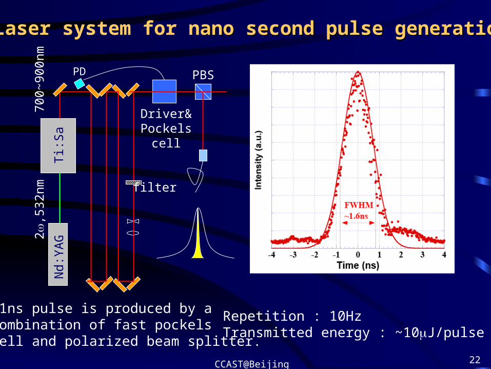
LaserLaser system for nano second pulse generationano second pulse generation
~1ns pulse is produced by a combination of fast pockels cell and polarized beam splitter.
Repetition : 10HzTransmitted energy : ~10J/pulse
2
,53
2nm
700
~900n
m
Driver&Pockels
cell
filter
Nd:
YAG
Ti:S
aPBSPD
CCAST@Beijing 23
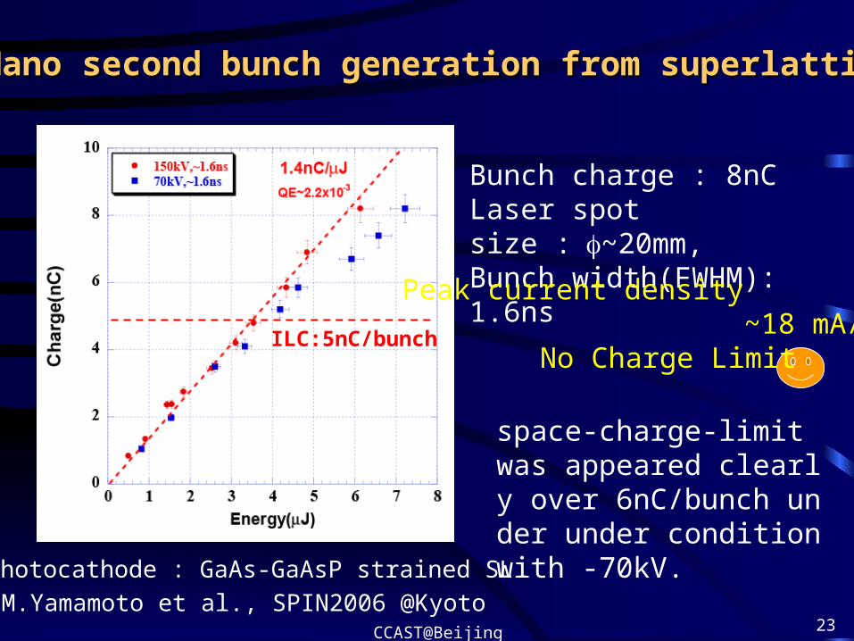
ILC:5nC/bunch
Nano second bunch generation from superlatticeano second bunch generation from superlattice
Photocathode : GaAs-GaAsP strained SL
Bunch charge : 8nCLaser spot size :~20mm,Bunch width(FWHM): 1.6ns
space-charge-limit was appeared clearly over 6nC/bunch under under condition with -70kV.
Peak current density ~18 mA/mm2
No Charge Limit
M.Yamamoto et al., SPIN2006 @Kyoto

CCAST@Beijing 24
Solenoid
4.8nC,16mm
0 0.15 0.5[m]
0.00 0.05 0.10 0.15 0.20 0.25 0.30 0.35 0.40 0.45 0.50
z [m]
-15
-10
-5
0
5
10
15
x [m
m]
anode
Solenoid
200kV,1.0ns,4.8nC
Norm. x.rms ~ 8.8 .mm.mrad with optimization emittance compensation by solenoid.
Emittance simulation

CCAST@Beijing 25
Emittance Measurement System
Pepper Pot Mask (40m holes)
Plastic sintillator

CCAST@Beijing 26
N. Yamamoto et al., J. Appl. Phys. 102, 024904 (2007)
Measurement of ~1ns, 5nC bunch is progressing.

CCAST@Beijing 27
Summary(1)
Photocathode
High Voltage GunUltrahigh Vacuum
High Field gradient
Polarized Electron Source
Laser
GaAs-GaAsP strained superlattice
UHV (2.2x10⁻⁹ Pa) was achieved.Lifetime measurement under progressing…
under developing…(Ti-Sapphire laser system is planed by SLAC)
Pol ≥ 85%, Q.E ≥ 0.5% are demonstrated.
200kV (3MV/m@photocathode) operation for> 200 hours without breakdown, dark current ≤ 1nA

CCAST@Beijing 28
High polarization Pol.> 80% with high QE
High beam current Ipeak > 5A, (>20mA/mm2)
Long lifetime ≥100 h, ≥ 65A operation
Low emittance Norm. x.rms ≤ 10 .mm.mrad
Multi bunch structure ≥5J/micropulse, (drive laser development) 2860micropulse/train
Summary(2)