High-Performance Sensors Based on Resistance Fluctuations ...
6
High-Performance Sensors Based on Resistance Fluctuations of Single-Layer-Graphene Transistors Kazi Rafsanjani Amin and Aveek Bid* Department of Physics, Indian Institute of Science, Bangalore, Karnataka, India 560012 ABSTRACT: One of the most interesting predicted applications of graphene- monolayer-based devices is as high-quality sensors. In this article, we show, through systematic experiments, a chemical vapor sensor based on the measurement of low- frequency resistance fluctuations of single-layer-graphene field-effect-transistor devices. The sensor has extremely high sensitivity, very high specificity, high fidelity, and fast response times. The performance of the device using this scheme of measurement (which uses resistance fluctuations as the detection parameter) is more than 2 orders of magnitude better than a detection scheme in which changes in the average value of the resistance is monitored. We propose a number-density- fluctuation-based model to explain the superior characteristics of a noise- measurement-based detection scheme presented in this article. KEYWORDS: graphene, field-effect transistor, sensor, resistance fluctuations, noise, number-density fluctuation 1. INTRODUCTION Single-layer graphene (SLG) has several distinctly unique properties that make it exceptionally suited for use as material and radiation sensors. The specific surface area (2630 m 2 g −1 ) of SLG is among the highest in layered materials, 1 making the conductance of graphene extremely sensitive to the ambient; that is, the presence of a few foreign molecules on its surface can significantly modify its electrical characteristics. SLG is highly conductive even in very low carrier density regimes, with room temperature mobilities on the order of 20000 cm 2 V −1 s −1 routinely achievable. 2−4 This causes graphene-based devices to have much lower levels of thermal noise compared to semiconductor-based sensors having comparable carrier densities. The low defect levels of pristine graphene 5−8 ensure that intrinsic flicker noise due to thermal switching of defects is lower than that of any semiconductor material. 9−13 The ability of SLG to interact with materials with a variety of interactions, from weak van der Waals force to extremely stable covalent bonds, raises the possibility of detecting a wide variety of materials with SLG-based sensors with high specificity. Single- layer-graphene field-effect-transistor (SLG-FET) devices thus seem to have almost all of the properties required to be an effective sensor material: accessibility to large surface area, good transduction, electrical and mechanical stability, and ease of preparation. There have been previous reports of the use of graphene- based sensors to detect various chemical gas molecules like NH 3 , CO, NO 2 , NO, O 2 , CO 2 , and H 2 , 14,16−21 as well as biomolecules. 23,24 In all of these cases, the change in the resistance of the device was used as the detection parameter. The sensitivity obtained was at best a few percentage points with extremely long device reset times (on the order of tens of minutes to hours), making them unsuitable for any practical applications. This scenario motivates the development of alternate schemes of sensing, which allows fast detection of analytes with similar, if not improved, sensitivity. In a previous publication, we had reported a very high sensitivity of the intrinsic low-frequency resistance noise of SLG-FET devices to the nature of its ambient. We had also elucidated a probable mechanism behind the high sensitivity of the measured noise to changes in the ambient of the graphene device. 25 In this article, we present extensive studies of the sensing of specific gas molecules using resistance fluctuations (noise) of SLG-FET devices. The relative variance δR 2 /R 2 of resistance fluctuations of the devices was found to show reproducible changes upon exposure to many different chemical vapor molecules. The devices had extremely fast response and reset times, on the order of seconds. The sensitivity of the SLG-FET sensor using this technique was more than an order of magnitude better than sensing with the same device using changes in the resistance of the device. There have been previous demonstrations of the use of resistance fluctuations to detect adsorbed molecules, 26 but a systematic study of the sensitivity, specificity, and response times of the sensors based on this technique is missing. To work as an effective material sensor, a device must satisfy a certain basic set of criterion: (1) it should have a measurable response, (2) the response and reset times must be low, (3) its response must scale as the amount of test molecules in its working range, (4) the response must be reproducible, and (5) there should be selectivity in response to different types of test molecules. We show in this article that SLG-FET using resistance fluctuations as the detection parameter satisfies all of the above criterion extremely well. Received: July 2, 2015 Accepted: August 24, 2015 Published: August 24, 2015 Research Article www.acsami.org © 2015 American Chemical Society 19825 DOI: 10.1021/acsami.5b05922 ACS Appl. Mater. Interfaces 2015, 7, 19825−19830
Transcript of High-Performance Sensors Based on Resistance Fluctuations ...
High-Performance Sensors Based on Resistance Fluctuations ofSingle-Layer-Graphene TransistorsKazi Rafsanjani Amin and Aveek Bid*
Department of Physics, Indian Institute of Science, Bangalore, Karnataka, India 560012
ABSTRACT: One of the most interesting predicted applications of graphene-monolayer-based devices is as high-quality sensors. In this article, we show, throughsystematic experiments, a chemical vapor sensor based on the measurement of low-frequency resistance fluctuations of single-layer-graphene field-effect-transistordevices. The sensor has extremely high sensitivity, very high specificity, highfidelity, and fast response times. The performance of the device using this scheme ofmeasurement (which uses resistance fluctuations as the detection parameter) ismore than 2 orders of magnitude better than a detection scheme in which changesin the average value of the resistance is monitored. We propose a number-density-fluctuation-based model to explain the superior characteristics of a noise-measurement-based detection scheme presented in this article.
KEYWORDS: graphene, field-effect transistor, sensor, resistance fluctuations, noise, number-density fluctuation
1. INTRODUCTION
Single-layer graphene (SLG) has several distinctly uniqueproperties that make it exceptionally suited for use as materialand radiation sensors. The specific surface area (2630 m2 g−1)of SLG is among the highest in layered materials,1 making theconductance of graphene extremely sensitive to the ambient;that is, the presence of a few foreign molecules on its surfacecan significantly modify its electrical characteristics. SLG ishighly conductive even in very low carrier density regimes, withroom temperature mobilities on the order of 20000 cm2 V−1 s−1
routinely achievable.2−4 This causes graphene-based devices tohave much lower levels of thermal noise compared tosemiconductor-based sensors having comparable carrierdensities. The low defect levels of pristine graphene5−8 ensurethat intrinsic flicker noise due to thermal switching of defects islower than that of any semiconductor material.9−13 The abilityof SLG to interact with materials with a variety of interactions,from weak van der Waals force to extremely stable covalentbonds, raises the possibility of detecting a wide variety ofmaterials with SLG-based sensors with high specificity. Single-layer-graphene field-effect-transistor (SLG-FET) devices thusseem to have almost all of the properties required to be aneffective sensor material: accessibility to large surface area, goodtransduction, electrical and mechanical stability, and ease ofpreparation.There have been previous reports of the use of graphene-
based sensors to detect various chemical gas molecules likeNH3, CO, NO2, NO, O2, CO2, and H2,
14,16−21 as well asbiomolecules.23,24 In all of these cases, the change in theresistance of the device was used as the detection parameter.The sensitivity obtained was at best a few percentage pointswith extremely long device reset times (on the order of tens ofminutes to hours), making them unsuitable for any practicalapplications. This scenario motivates the development of
alternate schemes of sensing, which allows fast detection ofanalytes with similar, if not improved, sensitivity. In a previouspublication, we had reported a very high sensitivity of theintrinsic low-frequency resistance noise of SLG-FET devices tothe nature of its ambient. We had also elucidated a probablemechanism behind the high sensitivity of the measured noise tochanges in the ambient of the graphene device.25 In this article,we present extensive studies of the sensing of specific gasmolecules using resistance fluctuations (noise) of SLG-FETdevices. The relative variance δR2/R2 of resistance fluctuationsof the devices was found to show reproducible changes uponexposure to many different chemical vapor molecules. Thedevices had extremely fast response and reset times, on theorder of seconds. The sensitivity of the SLG-FET sensor usingthis technique was more than an order of magnitude betterthan sensing with the same device using changes in theresistance of the device.There have been previous demonstrations of the use of
resistance fluctuations to detect adsorbed molecules,26 but asystematic study of the sensitivity, specificity, and responsetimes of the sensors based on this technique is missing. Towork as an effective material sensor, a device must satisfy acertain basic set of criterion: (1) it should have a measurableresponse, (2) the response and reset times must be low, (3) itsresponse must scale as the amount of test molecules in itsworking range, (4) the response must be reproducible, and (5)there should be selectivity in response to different types of testmolecules. We show in this article that SLG-FET usingresistance fluctuations as the detection parameter satisfies all ofthe above criterion extremely well.
Received: July 2, 2015Accepted: August 24, 2015Published: August 24, 2015
Research Article
www.acsami.org
© 2015 American Chemical Society 19825 DOI: 10.1021/acsami.5b05922ACS Appl. Mater. Interfaces 2015, 7, 19825−19830
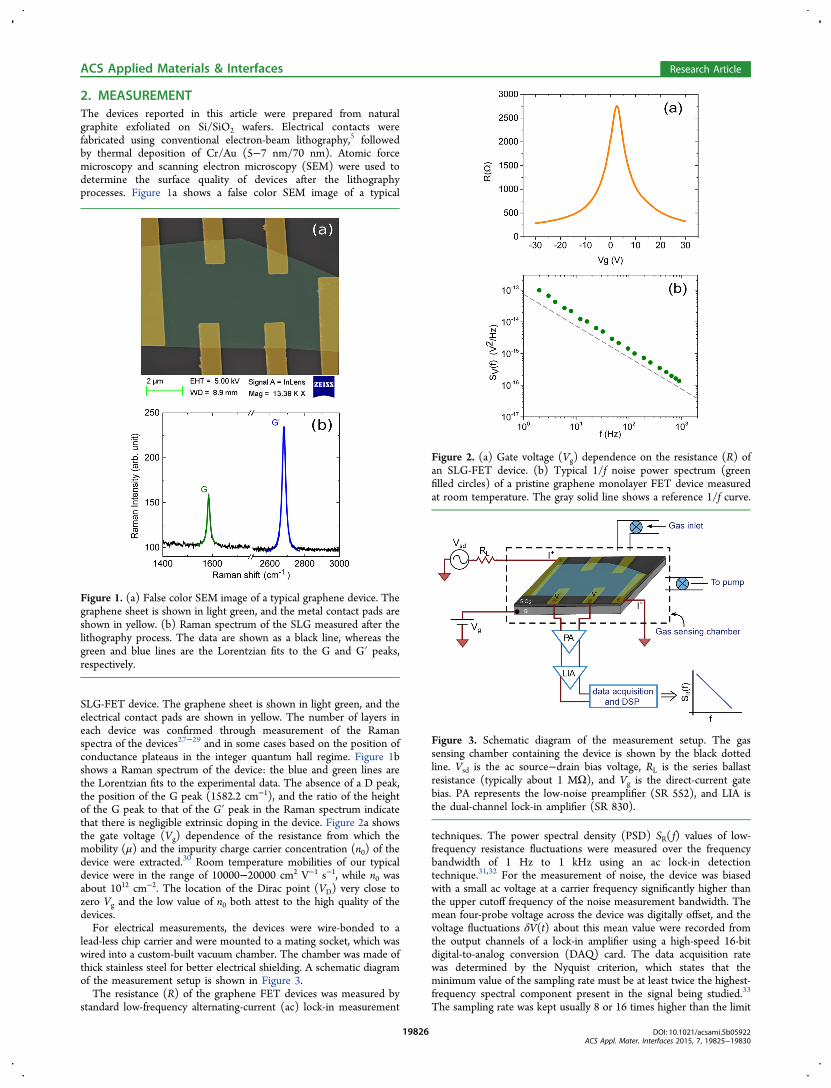
2. MEASUREMENTThe devices reported in this article were prepared from naturalgraphite exfoliated on Si/SiO2 wafers. Electrical contacts werefabricated using conventional electron-beam lithography,5 followedby thermal deposition of Cr/Au (5−7 nm/70 nm). Atomic forcemicroscopy and scanning electron microscopy (SEM) were used todetermine the surface quality of devices after the lithographyprocesses. Figure 1a shows a false color SEM image of a typical
SLG-FET device. The graphene sheet is shown in light green, and theelectrical contact pads are shown in yellow. The number of layers ineach device was confirmed through measurement of the Ramanspectra of the devices27−29 and in some cases based on the position ofconductance plateaus in the integer quantum hall regime. Figure 1bshows a Raman spectrum of the device: the blue and green lines arethe Lorentzian fits to the experimental data. The absence of a D peak,the position of the G peak (1582.2 cm−1), and the ratio of the heightof the G peak to that of the G′ peak in the Raman spectrum indicatethat there is negligible extrinsic doping in the device. Figure 2a showsthe gate voltage (Vg) dependence of the resistance from which themobility (μ) and the impurity charge carrier concentration (n0) of thedevice were extracted.30 Room temperature mobilities of our typicaldevice were in the range of 10000−20000 cm2 V−1 s−1, while n0 wasabout 1012 cm−2. The location of the Dirac point (VD) very close tozero Vg and the low value of n0 both attest to the high quality of thedevices.For electrical measurements, the devices were wire-bonded to a
lead-less chip carrier and were mounted to a mating socket, which waswired into a custom-built vacuum chamber. The chamber was made ofthick stainless steel for better electrical shielding. A schematic diagramof the measurement setup is shown in Figure 3.The resistance (R) of the graphene FET devices was measured by
standard low-frequency alternating-current (ac) lock-in measurement
techniques. The power spectral density (PSD) SR( f) values of low-frequency resistance fluctuations were measured over the frequencybandwidth of 1 Hz to 1 kHz using an ac lock-in detectiontechnique.31,32 For the measurement of noise, the device was biasedwith a small ac voltage at a carrier frequency significantly higher thanthe upper cutoff frequency of the noise measurement bandwidth. Themean four-probe voltage across the device was digitally offset, and thevoltage fluctuations δV(t) about this mean value were recorded fromthe output channels of a lock-in amplifier using a high-speed 16-bitdigital-to-analog conversion (DAQ) card. The data acquisition ratewas determined by the Nyquist criterion, which states that theminimum value of the sampling rate must be at least twice the highest-frequency spectral component present in the signal being studied.33
The sampling rate was kept usually 8 or 16 times higher than the limit
Figure 1. (a) False color SEM image of a typical graphene device. Thegraphene sheet is shown in light green, and the metal contact pads areshown in yellow. (b) Raman spectrum of the SLG measured after thelithography process. The data are shown as a black line, whereas thegreen and blue lines are the Lorentzian fits to the G and G′ peaks,respectively.
Figure 2. (a) Gate voltage (Vg) dependence on the resistance (R) ofan SLG-FET device. (b) Typical 1/f noise power spectrum (greenfilled circles) of a pristine graphene monolayer FET device measuredat room temperature. The gray solid line shows a reference 1/f curve.
Figure 3. Schematic diagram of the measurement setup. The gassensing chamber containing the device is shown by the black dottedline. Vsd is the ac source−drain bias voltage, RL is the series ballastresistance (typically about 1 MΩ), and Vg is the direct-current gatebias. PA represents the low-noise preamplifier (SR 552), and LIA isthe dual-channel lock-in amplifier (SR 830).
ACS Applied Materials & Interfaces Research Article
DOI: 10.1021/acsami.5b05922ACS Appl. Mater. Interfaces 2015, 7, 19825−19830
19826
given by Nyquist’s sampling theorem, and the time series of resistancefluctuations were recorded in contiguous segments of 30 s each. Theacquired data were antialiased digitally and down-sampled. The PSDof resistance fluctuations SR( f) was estimated using Welch’s averagedperiodogram method.34 This technique of noise measurement31,32
allows for a simultaneous measurement of both the intrinsic resistancefluctuations of the device and the background noise arising fromthermal fluctuations as well as instrumentation noise. A typical PSD,SR( f) of resistance fluctuations, of the SLG-FET measured at roomtemperature is shown in Figure 2b as a function of the frequency f.The resistance fluctuation spectra of pristine graphene devices werealways found to be 1/f in nature over the entire bandwidth ofmeasurement.The PSD SR( f) integrated over the frequency bandwidth of
measurement and normalized by the square of the average resistancevalue gives the relative variance of the resistance fluctuations δR2/R2
(which we refer to as noise):
∫δ =RR R
fS f f1
( ) df
f2
2 2 Rmin
max
(1)
Here fmin and fmax are respectively the lower and upper bounds of themeasurement bandwidth.Graphene has a small but finite work-function difference with metal
contact probes, and the fluctuations in the Fermi level near the contactregion can generate measurable resistance fluctuations. To address thisissue, we have measured δR2/R2 of the device at different appliedsource−drain voltages Vsd. We find that the measured noise alwaysscales with the square of the applied voltage Vsd (to within ±5%),showing that the contribution of the contact noise to the observedeffect is negligible.25 As discussed later in this article, we also find thatthe measured noise has a strong dependence on the gate voltage Vg,suggesting that the major contribution to the measured noise arisesfrom the bulk of the device and not at the contacts.
3. RESULTS AND DISCUSSION
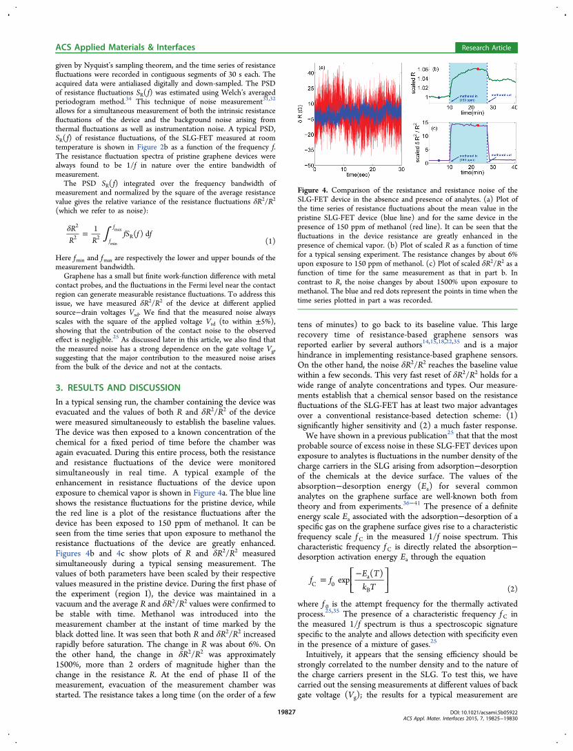
In a typical sensing run, the chamber containing the device wasevacuated and the values of both R and δR2/R2 of the devicewere measured simultaneously to establish the baseline values.The device was then exposed to a known concentration of thechemical for a fixed period of time before the chamber wasagain evacuated. During this entire process, both the resistanceand resistance fluctuations of the device were monitoredsimultaneously in real time. A typical example of theenhancement in resistance fluctuations of the device uponexposure to chemical vapor is shown in Figure 4a. The blue lineshows the resistance fluctuations for the pristine device, whilethe red line is a plot of the resistance fluctuations after thedevice has been exposed to 150 ppm of methanol. It can beseen from the time series that upon exposure to methanol theresistance fluctuations of the device are greatly enhanced.Figures 4b and 4c show plots of R and δR2/R2 measuredsimultaneously during a typical sensing measurement. Thevalues of both parameters have been scaled by their respectivevalues measured in the pristine device. During the first phase ofthe experiment (region I), the device was maintained in avacuum and the average R and δR2/R2 values were confirmed tobe stable with time. Methanol was introduced into themeasurement chamber at the instant of time marked by theblack dotted line. It was seen that both R and δR2/R2 increasedrapidly before saturation. The change in R was about 6%. Onthe other hand, the change in δR2/R2 was approximately1500%, more than 2 orders of magnitude higher than thechange in the resistance R. At the end of phase II of themeasurement, evacuation of the measurement chamber wasstarted. The resistance takes a long time (on the order of a few
tens of minutes) to go back to its baseline value. This largerecovery time of resistance-based graphene sensors wasreported earlier by several authors14,15,18,22,35 and is a majorhindrance in implementing resistance-based graphene sensors.On the other hand, the noise δR2/R2 reaches the baseline valuewithin a few seconds. This very fast reset of δR2/R2 holds for awide range of analyte concentrations and types. Our measure-ments establish that a chemical sensor based on the resistancefluctuations of the SLG-FET has at least two major advantagesover a conventional resistance-based detection scheme: (1)significantly higher sensitivity and (2) a much faster response.We have shown in a previous publication25 that that the most
probable source of excess noise in these SLG-FET devices uponexposure to analytes is fluctuations in the number density of thecharge carriers in the SLG arising from adsorption−desorptionof the chemicals at the device surface. The values of theabsorption−desorption energy (Ea) for several commonanalytes on the graphene surface are well-known both fromtheory and from experiments.36−41 The presence of a definiteenergy scale Ea associated with the adsorption−desorption of aspecific gas on the graphene surface gives rise to a characteristicfrequency scale f C in the measured 1/f noise spectrum. Thischaracteristic frequency f C is directly related the absorption−desorption activation energy Ea through the equation
=−⎡
⎣⎢⎤⎦⎥f f
E Tk T
exp( )
C 0a
B (2)
where f 0 is the attempt frequency for the thermally activatedprocess.25,35 The presence of a characteristic frequency f C inthe measured 1/f spectrum is thus a spectroscopic signaturespecific to the analyte and allows detection with specificity evenin the presence of a mixture of gases.25
Intuitively, it appears that the sensing efficiency should bestrongly correlated to the number density and to the nature ofthe charge carriers present in the SLG. To test this, we havecarried out the sensing measurements at different values of backgate voltage (Vg); the results for a typical measurement are
Figure 4. Comparison of the resistance and resistance noise of theSLG-FET device in the absence and presence of analytes. (a) Plot ofthe time series of resistance fluctuations about the mean value in thepristine SLG-FET device (blue line) and for the same device in thepresence of 150 ppm of methanol (red line). It can be seen that thefluctuations in the device resistance are greatly enhanced in thepresence of chemical vapor. (b) Plot of scaled R as a function of timefor a typical sensing experiment. The resistance changes by about 6%upon exposure to 150 ppm of methanol. (c) Plot of scaled δR2/R2 as afunction of time for the same measurement as that in part b. Incontrast to R, the noise changes by about 1500% upon exposure tomethanol. The blue and red dots represent the points in time when thetime series plotted in part a was recorded.
ACS Applied Materials & Interfaces Research Article
DOI: 10.1021/acsami.5b05922ACS Appl. Mater. Interfaces 2015, 7, 19825−19830
19827

plotted in Figure 5a. The green open circles are the relativevariance δR2/R2 measured before the sensing experiment. The
noise as a function of Vg has the symmetric M shape typical ofhigh-quality SLG devices. After each measurement, themeasurement chamber was pumped out and the noisemeasured again as a function of the gate voltage. It was seenthat the noise in the device after the analyte was pumped outalways came back to the baseline value of the pristine SLG-FET, as shown by the blue filled circles in Figure 5a.The red curve represents the noise δR2/R2 measured after
the device has been exposed to 25 ppm of methanol. We notethat there are two important features of the graph. First, thenoise is greatly enhanced at all values of Vg in comparison tothat in the pristine device. The second interesting feature is thatthe measured noise is no longer symmetric about the Diracpoint; for a given amount of a certain analyte, the measurednoise was seen to increase as the gate voltage was progressivelymade positive. In other words, the response of the graphenemonolayer, when exposed to a fixed amount of analyte, was notsymmetric in the electron- and hole-doped regimes; theresponse was much stronger in the electron-doped regime(Vg − VD > 0) than in the hole-doped regime (Vg − VD < 0).The slope of the noise plots as a function of the gate voltage athigh values of |Vg − VD|, where VD is the Dirac point ofgraphene, was seen to scale almost linearly with the amount ofanalyte. This can be seen clearly in Figure 5b, where we plot thenoise as a function of Vg in the presence of variousconcentrations of methanol. The evolution of the shape ofthe noise plots as a function of Vg for different levels ofexposure to the analyte can be explained using the followinganalysis: if the dominant source of resistance noise in thesedevices upon exposure to the analyte is fluctuations in thenumber density n of charge carriers in the conducting channel,then the following relation holds: δR = (δR/δn) δn. Becausethe carrier concentration is controlled by the back gate voltageVg, the contribution to the resistance noise from number-density fluctuations would be δR2/R2 ∝ (dR/dVg)
2/R2.12 Thevalues of (dR/dVg)
2/R2 calculated from the measured R−Vgcurves are plotted on the right axis in Figure 5b. There is a very
good qualitative match between the experimental data andcalculated plots. This shows that for the SLG-FET devicesexposed to chemicals number-density fluctuations are mostprobably the primary source of resistance fluctuation noise.To test the scaling of the response of the SLG sensor with
the concentration of the analytes, measurements similar tothose described above were performed by exposing the SLG-FET sensor to different amounts of chemicals. The resultsobtained for methanol vapor ranging in concentration from 20to 300 ppm are summarized in Figure 6. Figure 6a shows the
δR2/R2 values with time for consecutive measurements carriedout with different concentrations of methanol vapor. In theplot, the values of δR2/R2 have been scaled by the baselinevalue of δR2/R2 measured in the pristine SLG device. Note thatin each case the value of the relative variance δR2/R2 resets tothe initial state as the methanol vapor is pumped out. Theaverage increase in δR2/R2 after the device had been exposed tomethanol normalized by the baseline value of δR2/R2 is plottedin Figure 6b. The relative variance of resistance fluctuationsδR2/R2 was found to increase with the amount of analytepresent in the measurement chamber; this scaling behavior wasreproducible over several devices.To test the reproducibility of our sensing scheme with noise,
the SLG device was exposed to the same amount of methanolmultiple times. After each exposure, the device chamber wasevacuated and it was ensured that the noise went down to thebaseline value. A representative result is shown in Figure 7,where the normalized δR2/R2 is plotted as a function of time.From the plot, it can be seen that every time the device wasexposed to 100 ppm of methanol vapor the relative variance ofresistance fluctuations δR2/R2 scaled up to the same averagevalue, and upon pumping, it sharply reset to the initial state. Fordetection of 100 ppm of methanol, the observed spread in theaverage value corresponds to an error in the detection of 0.20ppm, attesting to the high fidelity of the sensor response.Our sensing scheme based on noise measurements was
tested using different types of molecules. The qualitative trendof fast response and high sensitivity was observed for all of thechemicals tested. The quantitative response of δR2/R2 to vaporsof different chemicals varied, ranging from a ∼70% change forchloroform to a ∼300% change in the case of nitrobenzene. In
Figure 5. (a) Plots of δR2/R2 as a function of the reduced gate voltage(Vg − VD) of the pristine SLG-FET device (green open circles), afterthe introduction of 25 ppm of methanol to the measurement chamber(red filled circles) and after the methanol vapor has been pumped out(blue filled circles). (b) Plots of δR2/R2 as a function of the reducedgate voltage (Vg − VD) after the SLG-FET has been exposed todifferent amounts of methanol vapor: 1 ppm (magenta open circles);25 ppm (blue open squares); 50 ppm (green filled diamonds); 75 ppm(red filled circles). (right axis) Plot of 1/R (dR/dVg)
2 for 50 ppm ofmethanol (green line) and 75 ppm of methanol (red line). Figure 6. (a) Plot of the relative variance δR2/R2 of the SLG-FET
device when exposed to different amounts of methanol vapor rangingfrom 20 to 200 ppm. Very small response and reset times wereobserved in all cases. (b) Plot of the average saturation value of δR2/R2
in the presence of different concentrations of methanol vapor. Thedata have been normalized by the baseline value of δR2/R2 beforeexposure to methanol. Inset: R−Vg plots measured in the presence ofdifferent amounts of methanol vapor.
ACS Applied Materials & Interfaces Research Article
DOI: 10.1021/acsami.5b05922ACS Appl. Mater. Interfaces 2015, 7, 19825−19830
19828

Figure 8, we plot the response of the SLG sensor exposed to100 ppm vapors of methanol, ammonia, chloroform, and
nitrobenzene. We were especially interested in the detection ofnitrobenzene because nitro group chemicals are extensivelyused in explosives. In our measurements, δR2/R2 in thegraphene device was observed to be highly sensitive to thepresence of nitrobenzene even at very low concentration,making it a very promising sensor for the detection ofexplosives.We currently do not have a clear understanding of the strong
response of the SLG-FET sensor to nitrobenzene. It has beenpredicted that the NO2 functional group associated withnitrobenzene has a very strong affinity with graphene, whichcan result in strong scattering centers. A dynamic fluctuation ofa strong scattering potential, resulting from the absorption−desprption of nitrobenzene, might lead to the high noise levelsmeasured. We believe that further experimental and theoreticalwork is needed to address this issue.
4. CONCLUSIONIn conclusion, we present experiments testing the efficacy ofgraphene-monolayer FET-based devices as chemical sensors.We find that a detection scheme based on measurements of theresistance fluctuations is far superior to the traditional methodof measuring the average resistance change in terms of the
sensitivity, specificity, and response time of the detector. Weshow that, for monolayer graphene devices exposed to theambient, the most likely source of enhanced resistancefluctuations is fluctuation in the carrier number density. Tothe best of our knowledge, graphene-based chemical sensorswith these characteristics have not been reported before.
■ AUTHOR INFORMATIONCorresponding Author*E-mail: [email protected] authors declare no competing financial interest.
■ ACKNOWLEDGMENTSThe authors thank the NPMASS, Government of India, forsupport. The authors thank device fabrication and character-ization facilities at the National Nanofabrication Centre andMicro and Nano Characterization Facility in the Centre forNano Science and Engineering at IISc, Bangalore. K.R.A. thanksthe CSIR, MHRDG, Government of India, for support.
■ REFERENCES(1) Pumera, M.; Ambrosi, A.; Bonanni, A.; Chng, E. L. K.; Poh, H. L.Graphene for Electrochemical Sensing and Biosensing. TrAC, TrendsAnal. Chem. 2010, 29, 954−965.(2) Soldano, C.; Mahmood, A.; Dujardin, E. Production, Propertiesand Potential of Graphene. Carbon 2010, 48, 2127−2150.(3) Zheng, M.; Takei, K.; Hsia, B.; Fang, H.; Zhang, X.; Ferralis, N.;Ko, H.; Chueh, Y.-L.; Zhang, Y.; Maboudian, R.; Javey, A. Metal-catalyzed Crystallization of Amorphous Carbon to Graphene. Appl.Phys. Lett. 2010, 96, 063110.(4) Abergel, D. S. L.; Apalkov, V.; Berashevich, J.; Ziegler, K.;Chakraborty, T. Properties of Graphene: a Theoretical perspective.Adv. Phys. 2010, 59, 261−482.(5) Novoselov, K. S.; Geim, A. K.; Morozov, S. V.; Jiang, D.; Zhang,Y.; Dubonos, S. V.; Grigorieva, I. V.; Firsov, A. A. Electric Field Effectin Atomically Thin Carbon Films. Science 2004, 306, 666−669.(6) PMID 18298094: Lin, Y.-M.; Avouris, P. Strong Suppression ofElectrical Noise in Bilayer Graphene Nanodevices. Nano Lett. 2008, 8,2119−2125.(7) Ratinac, K. R.; Yang, W.; Ringer, S. P.; Braet, F. TowardUbiquitous Environmental Gas Sensors - Capitalizing on the Promiseof Graphene. Environ. Sci. Technol. 2010, 44, 1167−1176.(8) Shao, Q.; Liu, G.; Teweldebrhan, D.; Balandin, A. A.;Rumyantsev, S.; Shur, M.; Yan, D. Flicker Noise in Bilayer GrapheneTransistors. IEEE Electron Device Lett. 2009, 30, 288−290.(9) Balandin, A. A. Low-frequency 1/f Noise in Graphene Devices.Nat. Nanotechnol. 2013, 8, 549−555.(10) Xu, G.; Torres, C. M., Jr; Zhang, Y.; Liu, F.; Song, E. B.; Wang,M.; Zhou, Y.; Zeng, C.; Wang, K. L. Effect of Spatial ChargeInhomogeneity on 1/f Noise Behavior in Graphene. Nano Lett. 2010,10, 3312−3317.(11) Pal, A. N.; Ghatak, S.; Kochat, V.; Sneha, E.; Sampathkumar, A.;Raghavan, S.; Ghosh, A. Microscopic Mechanism of 1/f Noise inGraphene: Role of Energy Band Dispersion. ACS Nano 2011, 5,2075−2081.(12) Kaverzin, A.; Mayorov, A. S.; Shytov, A.; Horsell, D. Impuritiesas a Source of 1/f Noise in Graphene. Phys. Rev. B: Condens. MatterMater. Phys. 2012, 85, 075435.(13) Pellegrini, B. 1/f Noise in Graphene. Eur. Phys. J. B 2013, 86, 1−12.(14) Schedin, F.; Geim, A.; Morozov, S.; Hill, E.; Blake, P.;Katsnelson, M.; Novoselov, K. Detection of Individual Gas MoleculesAdsorbed on Graphene. Nat. Mater. 2007, 6, 652−655.(15) Chen, G.; Paronyan, T. M.; Harutyunyan, A. R. Sub-ppt GasDetection with Pristine Graphene. Appl. Phys. Lett. 2012, 101, 053119.
Figure 7. Plot showing the reproducibility in the change of δR2/R2 ofthe SLG device for three consecutive runs with 100 ppm of methanol.
Figure 8. Plots of δR2/R2 during sensing experiments with the SLG-FET device exposed to 100 ppm of different chemicals: (a) methanol;(b) chloroform; (c) nitrobenzene; (d) ammonia.
ACS Applied Materials & Interfaces Research Article
DOI: 10.1021/acsami.5b05922ACS Appl. Mater. Interfaces 2015, 7, 19825−19830
19829
(16) Chen, C. W.; Hung, S. C.; Yang, M. D.; Yeh, C. W.; Wu, C. H.;Chi, G. C.; Ren, F.; Pearton, S. J. Oxygen Sensors made by MonolayerGraphene under Room Temperature. Appl. Phys. Lett. 2011, 99,243502.(17) Yoon, H. J.; Jun, D. H.; Yang, J. H.; Zhou, Z.; Yang, S. S.;Cheng, M. M.-C. Carbon dioxide Gas Sensor using a Graphene Sheet.Sens. Actuators, B 2011, 157, 310−313.(18) Wu, W.; Liu, Z.; Jauregui, L. A.; Yu, Q.; Pillai, R.; Cao, H.; Bao,J.; Chen, Y. P.; Pei, S.-S. Wafer-scale Synthesis of Graphene byChemical Vapor Deposition and its Application in Hydrogen Sensing.Sens. Actuators, B 2010, 150, 296−300.(19) Amin, K. R.; Bid, A. Graphene as a Sensor. Curr. Sci. 2014, 107,430−436.(20) Yavari, F.; Koratkar, N. Graphene-based Chemical Sensors. J.Phys. Chem. Lett. 2012, 3, 1746−1753.(21) Yuan, W.; Shi, G. Graphene-based Gas Sensors. J. Mater. Chem.A 2013, 1, 10078−10091.(22) Iezhokin, I.; Offermans, P.; Brongersma, S. H.; Giesbers, A. J.M.; Flipse, C. F. J. High Sensitive Quasi Freestanding EpitaxialGraphene Gas Sensor on 6H-SiC. Appl. Phys. Lett. 2013, 103, 053514.(23) Dong, X.; Shi, Y.; Huang, W.; Chen, P.; Li, L.-J. ElectricalDetection of DNA Hybridization with Single-Base Specificity UsingTransistors Based on CVD-Grown Graphene Sheets. Adv. Mater.(Weinheim, Ger.) 2010, 22, 1649−1653.(24) Dong, X.; Huang, W.; Chen, P. In situ Synthesis of ReducedGraphene Oxide and Gold Nanocomposites for Nanoelectronics andBiosensing. Nanoscale Res. Lett. 2010, 6, 60.(25) Amin, K. R.; Bid, A. Effect of Ambient on the ResistanceFluctuations of Graphene. Appl. Phys. Lett. 2015, 106, 183105.(26) Rumyantsev, S.; Liu, G.; Shur, M. S.; Potyrailo, R. A.; Balandin,A. A. Selective Gas Sensing with a Single Pristine Graphene Transistor.Nano Lett. 2012, 12, 2294−2298.(27) Ferrari, A. C.; Meyer, J. C.; Scardaci, V.; Casiraghi, C.; Lazzeri,M.; Mauri, F.; Piscanec, S.; Jiang, D.; Novoselov, K. S.; Roth, S.; Geim,A. K. Raman Spectrum of Graphene and Graphene Layers. Phys. Rev.Lett. 2006, 97, 187401.(28) Ferrari, A. C. Raman Spectroscopy of Graphene and Graphite:Disorder, Electron-Phonon Coupling, Doping and Nonadiabaticeffects. Solid State Commun. 2007, 143, 47−57.(29) Malard, L. M.; Pimenta, M. A.; Dresselhaus, G.; Dresselhaus, M.S. Raman Spectroscopy in Graphene. Phys. Rep. 2009, 473, 51.(30) Zhu, W.; Perebeinos, V.; Freitag, M.; Avouris, P. CarrierScattering, Mobilities, and Electrostatic Potential in Monolayer,Bilayer, and Trilayer Graphene. Phys. Rev. B: Condens. Matter Mater.Phys. 2009, 80, 235402.(31) Ghosh, A.; Kar, S.; Bid, A.; Raychaudhuri, A. A set-up forMeasurement of Low Frequency Conductance Fluctuation (Noise)using Digital Signal Processing techniques. arXiv.org, e-Print Arch.,Condens. Matter 2004.(32) Scofield, J. H. ac Method for Measuring Low-frequencyResistance Fluctuation Spectra. Rev. Sci. Instrum. 1987, 58, 985−993.(33) Shannon, C. E. Communication in the Presence of Noise. Proc.IRE 1949, 37, 10−21.(34) Welch, P. D. The use of Fast Fourier Transform for theEstimation of Power Spectra: A Method based on Time Averagingover Short, Modified Periodograms. IEEE Trans. Audio Electroacoust.1967, 15, 70−73.(35) Rumyantsev, S.; Liu, G.; Potyrailo, R.; Balandin, A.; Shur, M.Selective Sensing of Individual Gases Using Graphene Devices. IEEESens. J. 2013, 13, 2818−2822.(36) Pankewitz, T.; Klopper, W. Ab Initio Modeling of MethanolInteraction with Single-Walled Carbon Nanotubes. J. Phys. Chem. C2007, 111, 18917−18926.(37) Gautam, M.; Jayatissa, A. H. Graphene based Field EffectTransistor for the Detection of Ammonia. J. Appl. Phys. 2012, 112,064304.(38) Akesson, J.; Sundborg, O.; Wahlstrom, O.; Schroder, E. A vander Waals Density Functional study of Chloroform and otherTrihalomethanes on Graphene. J. Chem. Phys. 2012, 137, 174702.
(39) Lazar, P.; Karlicky, F.; Jurecka, P.; Kocman, M.; Otyepkova, E.;Safarova, K.; Otyepka, M. Adsorption of Small Organic Molecules onGraphene. J. Am. Chem. Soc. 2013, 135, 6372−6377.(40) Lin, X.; Ni, J.; Fang, C. Adsorption Capacity of H2O, NH3, CO,and NO2 on the Pristine Graphene. J. Appl. Phys. 2013, 113, 034306.(41) Huang, B.; Li, Z.; Liu, Z.; Zhou, G.; Hao, S.; Wu, J.; Gu, B.-L.;Duan, W. Adsorption of Gas Molecules on Graphene Nanoribbonsand Its Implication for Nanoscale Molecule Sensor. J. Phys. Chem. C2008, 112, 13442−13446.
ACS Applied Materials & Interfaces Research Article
DOI: 10.1021/acsami.5b05922ACS Appl. Mater. Interfaces 2015, 7, 19825−19830
19830