

High Performance Computing: Concepts, Methods & Means HPC Libraries
CSC 7600 Lecture 10 : Enabling TechSpring 2011
HIGH PERFORMANCE COMPUTING: MODELS, METHODS, &
MEANS
ENABLING TECHNOLOGIES
Prof. Thomas Sterling
Department of Computer Science
Louisiana State University
February 17, 2011

CSC 7600 Lecture 10 : Enabling TechSpring 2011
Topics
• Enabling Technologies - Introduction
• Processing Logic - CPU
• Memory Technology
• Communication - Concepts
• Intranode Communication (PCI, HT)
• Networking – Concepts
• Internode Communication (Ethernet, InfiniBand)
• Summary Materials for Test
2

CSC 7600 Lecture 10 : Enabling TechSpring 2011
Topics
• Enabling Technologies - Introduction
• Processing Logic - CPU
• Memory Technology
• Communication - Concepts
• Intranode Communication (PCI, HT)
• Networking – Concepts
• Internode Communication (Ethernet, InfiniBand)
• Summary Materials for Test
3

CSC 7600 Lecture 10 : Enabling TechSpring 2011
Enabling Technologies for Computing
Definition of Technology
• Merriam-Webster: the practical application of knowledge especially in particular area
• Greek etymology: techne (craft) and logia (saying)
• Technology breakthroughs enable leaps in computational performance and efficiency
• The necessity to overcome particular system bottlenecks drives technological development
• The performance limitations occur at certain classes of system components– Resolving them frequently shifts them to a different part of the system
– Applying solution to only one technological class is not going to work in the long term (synergy)
• The bottlenecks arise because one or more of the “four horsemen” become dominant factor(s) at a given technology point– Starvation
– Latency
– Overhead
– Waiting (Contention)
4

CSC 7600 Lecture 10 : Enabling TechSpring 2011 5
Evolution of HPC
1 103 106 109 10121015
KiloOPS MegaOPS GigaOPS TeraOPS PetaOPSOne OPS
1951Univac 1
1949Edsac
1976Cray 1
1982Cray XMP
1988Cray YMP
1964CDC 6600
1996T3E
1823 Babbage Difference
Engine
1991Intel Delta
1997ASCI Red
2001Earth
Simulator
2003Cray X1
1943Harvard Mark 1
1959IBM 7094
2006BlueGene/L
2009Cray XT5

CSC 7600 Lecture 10 : Enabling TechSpring 2011
System Node Diagram
6
MPU
L1L2
MPU
L1L2
L3
M1 M2 Mn
Controller
S
S
NIC NICUSBPeripherals
JTAG
Legend MPU: MicroProcessor UnitL1, L2, L3: CachesM1, M2,..: Memory BanksS: StorageNIC: Network Interface Card
Ethernet
PCI-e
MPU
L1L2
MPU
L1L2
L3

CSC 7600 Lecture 10 : Enabling TechSpring 2011
Computing Technology Classes
• Processing logic
– Responsible for execution of programs
– Control logic, data paths & functional logic
– TTL, ECL, MOS, CMOS, RSFQ
• Memory
– Providing storage for computational data
– Caches, main memory, secondary storage, tertiary storage
– Flash memory
• Communication
– Takes care of data movement in the computing system
– Intranode communication using buses (PCI, HT)
– Internode communication using networks (Ethernet, InfiniBand)
7

CSC 7600 Lecture 10 : Enabling TechSpring 2011
Technology Classes and Related Metrics
• Microprocessors
– Clock rate
– Instructions per Cycles (CPI)
– Cores per socket
– Power
• Memory
– Access Times
– Bandwidth
– Capacity, Size
• Networking
– Bandwidth
– Latency
– Protocol (e.g., TCP/IP)
8

CSC 7600 Lecture 10 : Enabling TechSpring 2011
Topics
• Enabling Technologies - Introduction
• Processing Logic - CPU
• Memory Technology
• Communication - Concepts
• Intranode Communication (PCI, HT)
• Networking – Concepts
• Internode Communication (Ethernet, InfiniBand)
• Summary Materials for Test
9

CSC 7600 Lecture 10 : Enabling TechSpring 2011
Digital Logic
• Processing logic is a circuitry that governs the transformation of computational state through execution of instructions encoded in stored computer programs
• Various aspects of digital logic undergo different technological transformations; it is helpful to distinguish:– Functional logic
• Defines capabilities of a processor
• Includes functional units and blocks, such as floating-point unit or ALU
– Control logic• Relates to instruction decoding and interpretation
• Includes instruction decoders and schedulers, execution logic, and various circuits helping optimize the execution
– Data paths• Determine throughput of temporary processing data as well as the rates
of computed information output and raw information input
• Define bit-widths of internal data and control buses as well as the topology of the interconnects
10

CSC 7600 Lecture 10 : Enabling TechSpring 2011
Modern CPU Core Comparison
11
AMD K8 Intel Core2
CSC 7600 Lecture 10 : Enabling TechSpring 2011
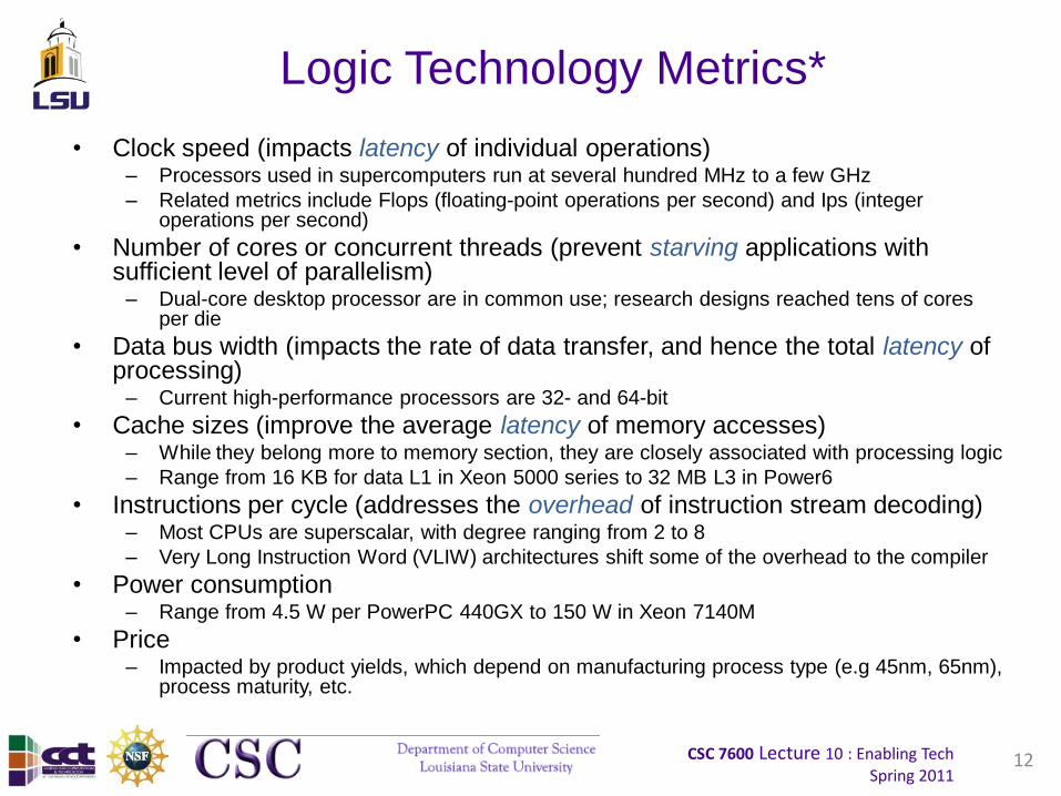
Logic Technology Metrics*
• Clock speed (impacts latency of individual operations)– Processors used in supercomputers run at several hundred MHz to a few GHz
– Related metrics include Flops (floating-point operations per second) and Ips (integer operations per second)
• Number of cores or concurrent threads (prevent starving applications with sufficient level of parallelism)
– Dual-core desktop processor are in common use; research designs reached tens of cores per die
• Data bus width (impacts the rate of data transfer, and hence the total latency of processing)
– Current high-performance processors are 32- and 64-bit
• Cache sizes (improve the average latency of memory accesses)– While they belong more to memory section, they are closely associated with processing logic
– Range from 16 KB for data L1 in Xeon 5000 series to 32 MB L3 in Power6
• Instructions per cycle (addresses the overhead of instruction stream decoding)– Most CPUs are superscalar, with degree ranging from 2 to 8
– Very Long Instruction Word (VLIW) architectures shift some of the overhead to the compiler
• Power consumption– Range from 4.5 W per PowerPC 440GX to 150 W in Xeon 7140M
• Price– Impacted by product yields, which depend on manufacturing process type (e.g 45nm, 65nm),
process maturity, etc.
12

CSC 7600 Lecture 10 : Enabling TechSpring 2011
Evolution of Electrically Powered
Processing Logic
13
Relay computer Z3
Berlin, 1941
Clock 5.3 Hz (up to ~10 Hz)
4000 W power
Valve computer Colossus Mark II
Bletchley Park, 1944
Eff. 1 boolean operation per 0.4 µs Discrete transistor computer TRADIC
Bell Labs, 1955
1 mil. logical operations per sec.
100 W power usage
PDP-11/20, based on SSI integrated
circuits
Digital Equipment Corp., 1970
800 ns cycle
~400 W (more with expanded
configuration)
Single LSI microprocessor 4004
Intel, 1971
Clock 740 kHz, 0.07 MIPS
Power consumption < 500 mW

CSC 7600 Lecture 10 : Enabling TechSpring 2011
Clock Scaling of Intel CPUs
14
CSC 7600 Lecture 10 : Enabling TechSpring 2011
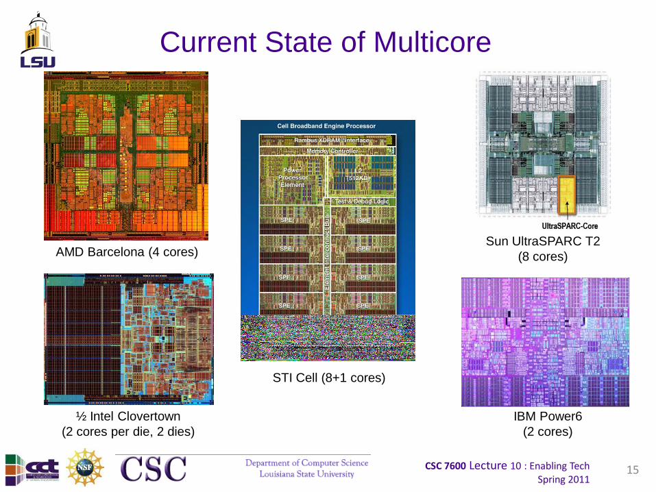
Current State of Multicore
15
Sun UltraSPARC T2
(8 cores)AMD Barcelona (4 cores)
STI Cell (8+1 cores)
IBM Power6
(2 cores)
½ Intel Clovertown
(2 cores per die, 2 dies)

CSC 7600 Lecture 10 : Enabling TechSpring 2011
Processor Parameter Comparison
16
Clock Speed(#cores)
Cache Sizes(per core)
IPC(per core)
Power
AMDOpteron (64-bit)
3.0 GHz (2) L1: 64+64KBL2: 1MB
2 FP, 3 Integer 119 W
IBM PowerPC 450 (32-bit)
0.85 GHz (4) L1: 32+32KBL2: ?L3: 8MB
4 FP, 2 Integer 16 W
Intel Itanium 29150M (64-bit)
1.66 GHz (2) L1: 16+16KBL2: 1024+256KBL3: 12MB
4 FP, 4 Integer 104 W
Intel Xeon 7140M (64-bit)
3.4 GHz (2) L1: 32+32KBL2: 2MB
4 FP, 3 Integer 150 W
MIPS64 (64-bit) 0.5 GHz (6) L1: 32+32KBL2: 256KB
2 FP, 2 Integer <6 W

CSC 7600 Lecture 10 : Enabling TechSpring 2011
Power Problem: Current Leakage
17
Gate oxide leakageSubthreshold leakage
V. Salapura, Next Generation Supercomputers

CSC 7600 Lecture 10 : Enabling TechSpring 2011
Power Scaling Problem
18
Static vs dynamic power
Courtesy: ITERContribution of leakage factors vs
decrasing gate length

CSC 7600 Lecture 10 : Enabling TechSpring 2011
Tackling Power Issues
• Switched capacitance loses– Reduction of core voltage (energy loses proportional to V2)
– Low-k interconnects (SiO2doped with F or carbon, porous SiO2)
• Parasitic capacitance loses– Silicon on insulator (SOI), created through high-temperature
annealing of substrate containing embedded oxygen-rich layer
• Charge mobility impediments– Strained silicon (e.g. grown on a Ge substrate)
• Subthreshold leakage– Source biasing
– Multi-threshold CMOS
– Sleep transistor sizing
• Gate oxide leakage (tunneling)– High-k material to increase gate capacitance (hafnium and
zirconium silicates and oxides)
19
CSC 7600 Lecture 10 : Enabling TechSpring 2011
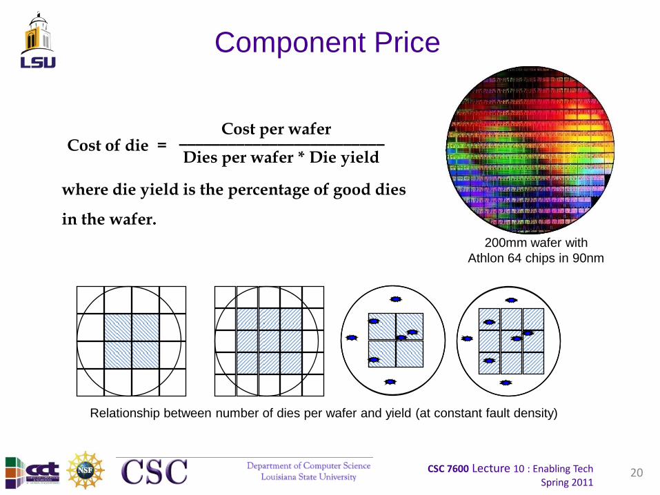
Component Price
20
_________________________Dies per wafer * Die yield
where die yield is the percentage of good dies
in the wafer.
Relationship between number of dies per wafer and yield (at constant fault density)
Cost per waferCost of die =
200mm wafer with
Athlon 64 chips in 90nm
CSC 7600 Lecture 10 : Enabling TechSpring 2011
Topics
• Enabling Technologies - Introduction
• Processing Logic - CPU
• Memory Technology
• Communication - Concepts
• Intranode Communication (PCI, HT)
• Networking – Concepts
• Internode Communication (Ethernet, InfiniBand)
• Summary Materials for Test
21

CSC 7600 Lecture 10 : Enabling TechSpring 2011
Memory• Serves as storage of computational state and instructions to transform
that state
• Organized in a hierarchy, ordered by increasing access latency and decreasing bandwidth:– Primary storage
• Directly accessible by the CPU
• Volatile (loses contents after power-down) in most cases today
• Includes: CPU registers, CPU caches, main memory
– Secondary storage• Not directly accessible by the CPU
• Data transfers accomplished through an intermediate area in primary storage and dedicated I/O channels
• Non-volatile
• Includes: hard disks, removable optical disks (CD and DVD drives), USB sticks, tape drives, etc.
– Tertiary storage• Involves automated (robotic) mechanisms mounting removable media on demand
• Includes: tape libraries, optical jukeboxes
– Off-line storage• Involves human interaction to handle the storage media
• Used for physical information transfer, e.g. to ensure information security
22

CSC 7600 Lecture 10 : Enabling TechSpring 2011
Memory Technology Metrics*
• Memory access latencies impact how quickly the information is available to the processor
– 100s of ps (CPU registers) to 10s…100s of ns (main memory) for primary storage
– Around 100µs for FLASH memory, several ms for hard drives, hundreds of ms for optical disks
– Single to tens of seconds for robotic storage libraries
• Memory bandwidth defines the maximum rate at which information is available for processing, preventing processor starvation
– 10s of GB/s for registers and L1 cache, single GB/s for main memory
– Ranges from 10s MB/s (optical media and FLASH) to 100s MB/s (high performance hard disks)
– Low 10s to over 100 MB/s for single tape drive; aggregate throughput may be much higher depending on aggregate number of devices
• Capacity: determines maximum problem size possible to compute (otherwise memory starvation and potential contention between competing processes/threads may result)
– Capacities range from few bytes per register, few of KB to tens of MB for CPU caches, 100s of GB to 1 TB for hard disks, and up to tens of PB for large tertiary storage systems
• Capacity density: determines additional costs associated with assembling storage of required capacity, such as volume, or device footprint
23

CSC 7600 Lecture 10 : Enabling TechSpring 2011
Evolution of Main Memory Technology
24
Mercury delay line memory
1000 words of 12 characters
400 µs latency
UNIVAC I, 1951
Williams tube
500 to 1000 bits
300..400 µs latency
Manchester Mark I, 1949
Drum memory
10000..20000 characters
2.4 ms average latency
IBM 650, 1954Core memory
Example capacity: 32x32 array
Cycle time: from 6 µs in 1951 down
to 600 ns in late 1970s
Semiconductor memory
Up to 4 Gb per DRAM
device
Cycle time: sub-10 ns
(SRAM)
Shown: Intel 1103 (1970)

CSC 7600 Lecture 10 : Enabling TechSpring 2011
Main Memory Implementations*
• Static Random Access Memory (SRAM)
– Fastest access time
– Modest power consumption per bit
– Relatively expensive to manufacture
– Discrete SRAM is slowly displaced in favor of PSRAM, which is
based on a DRAM equipped with an SRAM-like interface
• Dynamic Random Access Memory (DRAM)
– Cheapest production cost per bit
– Highest capacity per die area
• FLASH Memory
– Non-volatile
– Capacities approach those of DRAM
25

CSC 7600 Lecture 10 : Enabling TechSpring 2011
Static RAM*
• Uses a 6 MOSFET (6T) cell to store each bit– M5 and M6 are control transistors, biased through the
word line (WL), which is selected by address decoder
– M1..M4 form a bi-stable latch, with two possible stable states:
• M2, M3 on, M1, M4 off, corresponds to bit value 0
• M1, M4 on, M2, M3 off, represents bit value 1
– Each cell is connected to a bit line (BL) to communicate stored bit values to and from I/O logic
• Complementary bit lines (as in the figure) are frequently used to improve noise immunity and performance of some operations
• Memory with m address lines and n data lines operates 2m×n bit matrix
• Multiported memories are possible through addition of multiple BL pairs, WLs and control transistors (M5, M6) to each cell
• Operational and interface variants:– Asynchronous: no clock signal used
– Synchronous: data controlled by external clock signal
– ZBT (Zero Bus Turnaround): no additional latency when changing from read to write operation, and vice versa
– Pipeline Burst: may stream data effectively every clock cycle, but with latency exceeding single clock tick
26
SRAM Cell
Dual-ported SRAM from Cypress

CSC 7600 Lecture 10 : Enabling TechSpring 2011
Sample SRAM Block Diagrams
27
http://download.cypress.com.edgesuite.net/design_resources/datasheets/contents/cy7c1311cv18_8.pdf
Modern dual-ported 300 MHz QDR-II SRAMSimple asynchronous SRAM
http://download.cypress.com.edgesuite.net/design_resources/datasheets/contents/cy7c1009bn_8.pdf

CSC 7600 Lecture 10 : Enabling TechSpring 2011
Dynamic RAM*
• Stores each bit of data using only one transistor and one capacitor
• Lines connecting each row are word lines, the column lines are called bit lines
• Due to capacitor leakage, requires periodic refresh of stored charge (hence dynamic)
• The bit cells are organized in roughly square matrices, frequently multiple per die
– Banking permits parallel access to multiple matrices (bandwidth increase/latency reduction)
• DRAMs are typically designed with redundancy built-in
– Providing substitute rows in case of permanent faults (during production and use)
– Supplying storage for corrective codes to detect and correct soft errors (ECC)
• Several interface variants developed over years– Asynchronous (clock-less) vs. synchronous (SDRAM)
– Now practically obsolete: FPM, EDO, BEDO, “plain” SDRAM, Rambus DRAM (RDRAM)
– DDR (Double Data Rate), with DDR2, DDR3 variants
– XDR and XDR2 (next incarnation of Rambus interface)
– GDDR-n (n = 2, 3, 4, 5): specialized graphic memory
28
Schematic drawing based on the original DRAM patent (1968)

CSC 7600 Lecture 10 : Enabling TechSpring 2011
Currently Used SDRAM Variants*• DDR2
– Operates at twice the bus speed of DDR
– DDR2-1066 achieves 1066 million 64-bit transfers per second using 533 MHz bus clock (or 266 MHz memory clock)
• The corresponding module PC2-8500 has a peak bandwidth of over 8.5 GB/s, Cycle time 3.75 ns
– Module capacity: up to 4 GB
– Features 4-bit deep prefetch buffers
• DDR3
– Current successor of DDR2 with 30% lower power consumption (1.5 V supply) than DDR2
– Double the effective range of I/O clock to 800 MHz (with 200 MHz memory clock)
– 8-bit deep prefetch buffers
– DDR3-1600 (PC3-12800) achieves peak 12.8 GB/s with cycle time of 5 ns
• DDR4
– Will be the successor of DDR 3 and is expected to be available in 2012
– Expected to run at a supply voltage of 1.2V or less
– Expected to support an excess of 2 billion data transfers per second
29

CSC 7600 Lecture 10 : Enabling TechSpring 2011
Currently Used SDRAM Variants*
• GDDR5
– Provides twice I/O throughput compared to its immediate predecessor GDDR4
– Uses 8n prefetch architecture
– Clock rate up to 1.125 GHz, supporting data rate of 4.5GB/s
• XDR
– Next incarnation of Rambus RDRAM (differential open-collector driver)
– Clock rate up to 800 MHz, with planned 1066 MHz
– 8 or 16 lanes per chip, providing 3.2 or 6.4 GB/s at 400 MHz
– Eight memory banks, up to 4 bank-interleaved transactions at full bandwidth
– Used in small outline, high-bandwidth consumer applications (game consoles)
30

CSC 7600 Lecture 10 : Enabling TechSpring 2011
Block Diagram of Asynchronous DRAM
31
http://www.issi.com/pdf/41LV16105B.pdf

CSC 7600 Lecture 10 : Enabling TechSpring 2011
Block Diagram of DDR3 DRAM
32
http://download.micron.com/pdf/datasheets/dram/ddr3/1Gb%20DDR3%20SDRAM.pdf
CSC 7600 Lecture 10 : Enabling TechSpring 2011
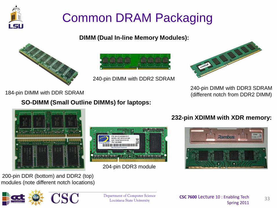
Common DRAM Packaging
33
184-pin DIMM with DDR SDRAM
200-pin DDR (bottom) and DDR2 (top)
modules (note different notch locations)
240-pin DIMM with DDR2 SDRAM
DIMM (Dual In-line Memory Modules):
240-pin DIMM with DDR3 SDRAM
(different notch from DDR2 DIMM)
SO-DIMM (Small Outline DIMMs) for laptops:
204-pin DDR3 module
232-pin XDIMM with XDR memory:
CSC 7600 Lecture 10 : Enabling TechSpring 2011
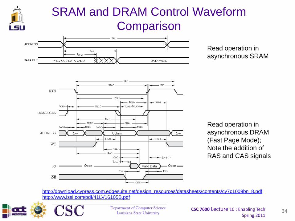
SRAM and DRAM Control Waveform
Comparison
34
http://download.cypress.com.edgesuite.net/design_resources/datasheets/contents/cy7c1009bn_8.pdf
http://www.issi.com/pdf/41LV16105B.pdf
Read operation in
asynchronous SRAM
Read operation in
asynchronous DRAM
(Fast Page Mode);
Note the addition of
RAS and CAS signals
CSC 7600 Lecture 10 : Enabling TechSpring 2011
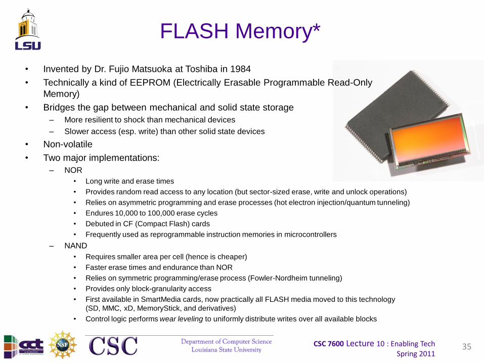
FLASH Memory*
• Invented by Dr. Fujio Matsuoka at Toshiba in 1984
• Technically a kind of EEPROM (Electrically Erasable Programmable Read-Only
Memory)
• Bridges the gap between mechanical and solid state storage
– More resilient to shock than mechanical devices
– Slower access (esp. write) than other solid state devices
• Non-volatile
• Two major implementations:
– NOR
• Long write and erase times
• Provides random read access to any location (but sector-sized erase, write and unlock operations)
• Relies on asymmetric programming and erase processes (hot electron injection/quantum tunneling)
• Endures 10,000 to 100,000 erase cycles
• Debuted in CF (Compact Flash) cards
• Frequently used as reprogrammable instruction memories in microcontrollers
– NAND
• Requires smaller area per cell (hence is cheaper)
• Faster erase times and endurance than NOR
• Relies on symmetric programming/erase process (Fowler-Nordheim tunneling)
• Provides only block-granularity access
• First available in SmartMedia cards, now practically all FLASH media moved to this technology
(SD, MMC, xD, MemoryStick, and derivatives)
• Control logic performs wear leveling to uniformly distribute writes over all available blocks
35

CSC 7600 Lecture 10 : Enabling TechSpring 2011
NOR and NAND FLASH Structures
36
NOR FLASH
Layout
NAND FLASH
Layout
CSC 7600 Lecture 10 : Enabling TechSpring 2011
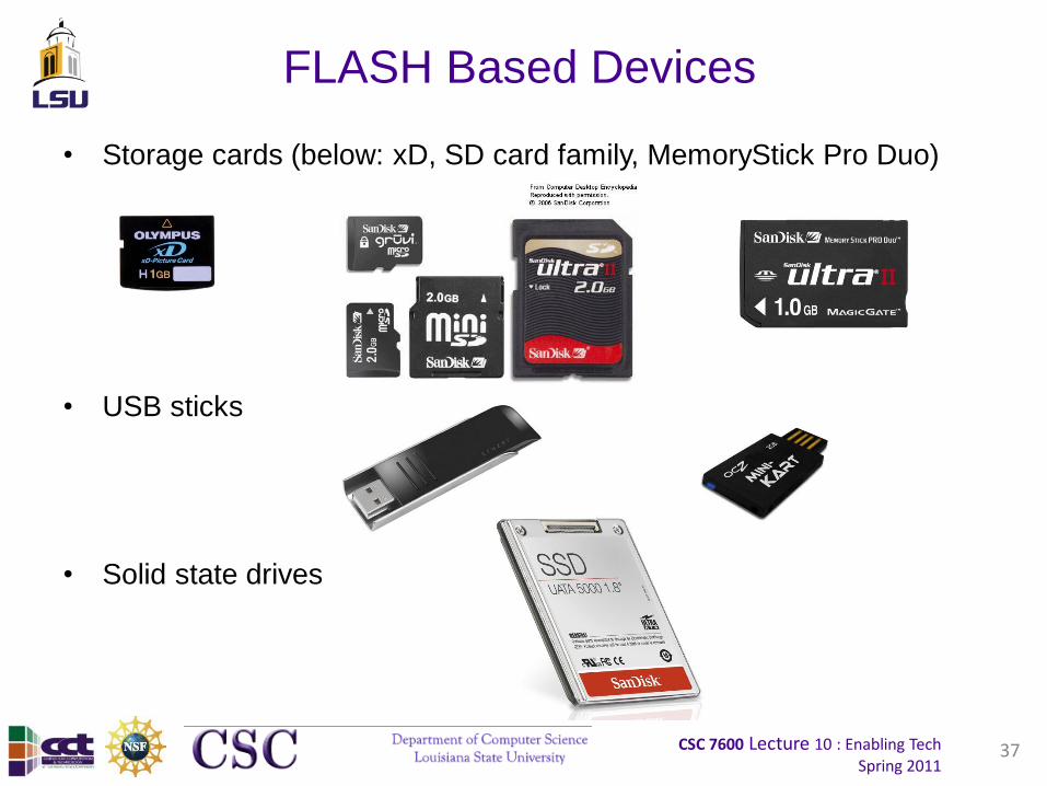
• Storage cards (below: xD, SD card family, MemoryStick Pro Duo)
• USB sticks
• Solid state drives
FLASH Based Devices
37

CSC 7600 Lecture 10 : Enabling TechSpring 2011
Secondary Storage: Hard Drives*
• Storage capacity: 2TB per drive
• Areal density: 400 Gbit/in2 (perpendicular recording)
• Rotational speed: 15,000 RPM
• Seek time– Track-to-track: 0.2 ms
– Average: 3.5 ms
– Full stroke: 6.7 ms
• Sustained transfer rate: up to 125 MB/s
• Non-recoverable error rate: 1 in 1017
• Interface bandwidth:– Fibre channel: 400 MB/s
– Serially Attached SCSI (SAS): 300 MB/s
– Ultra320 SCSI: 320 MB/s
– Serial ATA (SATA): 300 MB/s
38

CSC 7600 Lecture 10 : Enabling TechSpring 2011
Secondary Storage: Tape Drives
• Data are stored on magnetic tape– Only sequential access
– Long average seek times (average rewind time is around a minute)
• Streaming bandwidth rivals that of a single hard drive– SUN’s T10000 tape drive achieves a native
transfer rate of 120 MB/s
• Formats– Older proprietary format DLT (Digital Linear
Tape) featured up to 800 GB (DLT-S4) stored on a half-inch metal particle tape in a color-coded enclosure
– Linear Tape-Open (LTO) is an open alternative to DLT, initiated by Seagate, HP and IBM
• LTO-4 generation stores 800 GB per tape
• Two form factors: Accellis (8 mm, dual reel, oriented on fast access), and Ultrium (1/2”, single reel, promotes capacity)
• Supports data transfers up to 120 MB/s
• WORM and drive-level encryption capable
39
IBM TS1120 Tape Drive
HP SB920c Tape Blade
SUN T10000 Tape Drive

CSC 7600 Lecture 10 : Enabling TechSpring 2011
Tertiary Storage
• Tape library example: StorageTek SL8500– Modular system (extensible)
– Scales from 64 to 448 tape drives and from 1,448 to over 70,000 tape slots
– 50 tape slots per ft2
– In maximum configuration (32 libraries):
• Throughput: 193.2 TB/h (with T10000 drives)
• Capacity (uncompressed): 35 PB
• Avg. cell to drive per HandBot: <11 s
• Mean exchanges between failures (per bot): 2,000,000
• Footpad: 296.5”x2,338”
• Weight: 247,830 lb
– Robotics run oval path layout, achieving up to 1000 tape loads per hour; multiple robots possible
– Supports mixed tape (LTO, DLT) and drive types
– Hot swappable and redundant
40

CSC 7600 Lecture 10 : Enabling TechSpring 2011
Topics
• Enabling Technologies - Introduction
• Processing Logic - CPU
• Memory Technology
• Communication - Concepts
• Intranode Communication (PCI, HT)
• Networking – Concepts
• Internode Communication (Ethernet, InfiniBand)
• Summary Materials for Test
41

CSC 7600 Lecture 10 : Enabling TechSpring 2011
Communication Concepts*
• Latency is the delay of a transmission between the sender and the receiver.
• Throughput can be thought of as the maximum channel capacity between a sender and a receiver
• Intranode communication– Buses
– Northbridge / Southbridge
– PCI
– HT
• Internode communication– Network controller cards
– Network switch
– Network cables
42

CSC 7600 Lecture 10 : Enabling TechSpring 2011
Bus : History
• First generation– Microcomputer bus systems – essentially
passive backplane connected directly or through buffer amplifiers to the pins of the CPU
– Memory and other devices connected in parallel, to the bus using the same address & data pins as used in the CPU
– 8 bit parallel
– All the equipment using the bus had to talk at the same speed, as they share a single clock, increasing the speed to the CPU was hard as the devices had to be able to work at higher speeds as well
– Addition of expansion cards, involved jumpers, to set the memory address, I/O addresses, interrupt priorities, and interrupt numbers
43
8080 CPU
4K RAM
Tape Controller
S-100 Altair
CSC 7600 Lecture 10 : Enabling TechSpring 2011
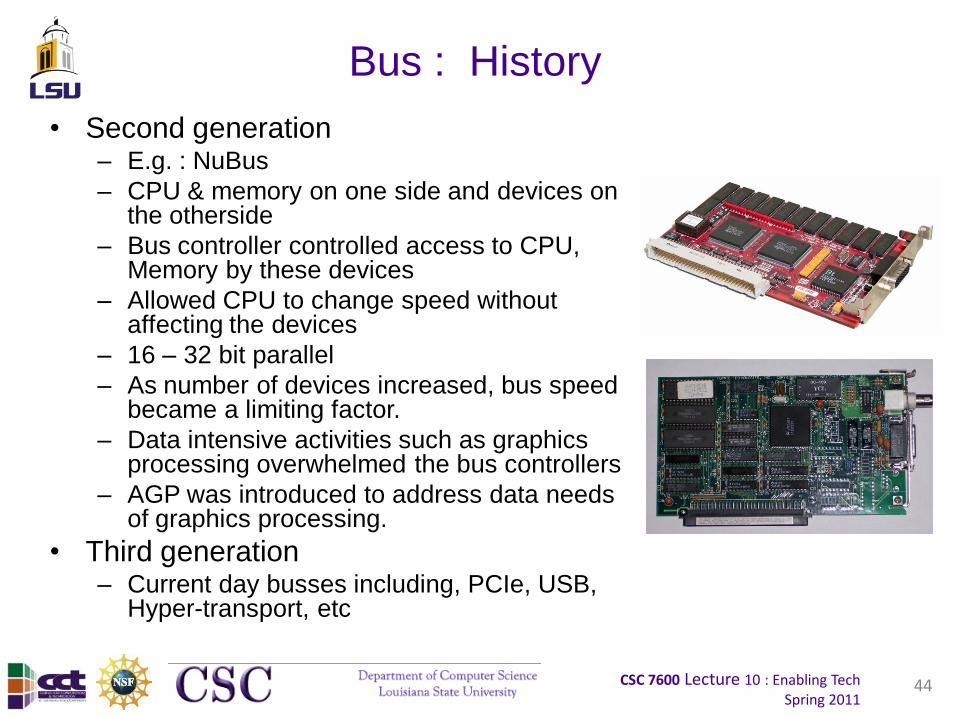
Bus : History
• Second generation– E.g. : NuBus
– CPU & memory on one side and devices on the otherside
– Bus controller controlled access to CPU, Memory by these devices
– Allowed CPU to change speed without affecting the devices
– 16 – 32 bit parallel
– As number of devices increased, bus speed became a limiting factor.
– Data intensive activities such as graphics processing overwhelmed the bus controllers
– AGP was introduced to address data needs of graphics processing.
• Third generation– Current day busses including, PCIe, USB,
Hyper-transport, etc
44

CSC 7600 Lecture 10 : Enabling TechSpring 2011
Buses
• Bus is a subsystem that transfers data between various components within a node
• Modern Bus subsystems can be used as both parallel and bit-serial connections – Can be wired as daisy chain topology,
connected by switched hubs, eg. USB
• Buses contain 3 main types of signal: Data, Address, Control
• Most buses are backplane components – Circuit board with parallel connectors into
which other boards are plugged perpendicularly
• Others are cable based components – Devices in separate chassis connected
together by cables that carry signals
45
PCI & ISA slots
PCI riser card
CSC 7600 Lecture 10 : Enabling TechSpring 2011
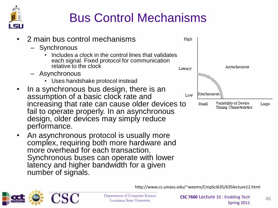
Bus Control Mechanisms
• 2 main bus control mechanisms – Synchronous
• Includes a clock in the control lines that validates each signal. Fixed protocol for communication relative to the clock
– Asynchronous• Uses handshake protocol instead
• In a synchronous bus design, there is an assumption of a basic clock rate and increasing that rate can cause older devices to fail to operate properly. In an asynchronous design, older devices may simply reduce performance.
• An asynchronous protocol is usually more complex, requiring both more hardware and more overhead for each transaction. Synchronous buses can operate with lower latency and higher bandwidth for a given number of signals.
46
http://www.cs.umass.edu/~weems/CmpSci635/635lecture12.html
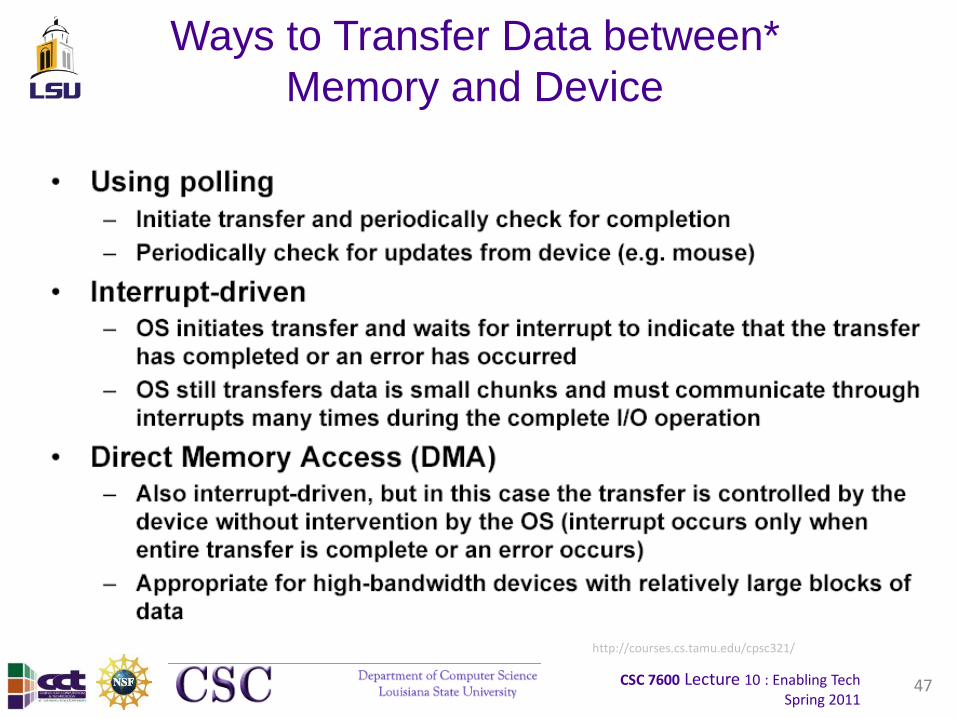
CSC 7600 Lecture 10 : Enabling TechSpring 2011
Ways to Transfer Data between*
Memory and Device
47
http://courses.cs.tamu.edu/cpsc321/

CSC 7600 Lecture 10 : Enabling TechSpring 2011
Overhead of Polling
48
http://courses.cs.tamu.edu/cpsc321/

CSC 7600 Lecture 10 : Enabling TechSpring 2011
Overhead of Polling
49
http://courses.cs.tamu.edu/cpsc321/

CSC 7600 Lecture 10 : Enabling TechSpring 2011
Topics
• Enabling Technologies - Introduction
• Processing Logic - CPU
• Memory Technology
• Communication - Concepts
• Intranode Communication (PCI, HT)
• Networking – Concepts
• Internode Communication (Ethernet, InfiniBand)
• Summary Materials for Test
50

CSC 7600 Lecture 10 : Enabling TechSpring 2011
Northbridge & Southbridge*
• Nortbridge– The Northbridge handles the communication
between the CPU, RAM, AGP or PCI Express and the southbridge
– Northbridge regulates the number, speed and type of CPU(s) and the amount, speed and type of RAM that can be used
– In AMD64 systems the memory controller handles the communication between the CPU and RAM
• Southbridge– Also known as the I/O controller hub, the
southbridge traditionally handles devices with slower capabilities
– Manages PCI bus, ISA bus, DMA controller, IDE (SATA / PATA Controller), onboard network controller and more
51
Northbridge Southbridge
CSC 7600 Lecture 10 : Enabling TechSpring 2011
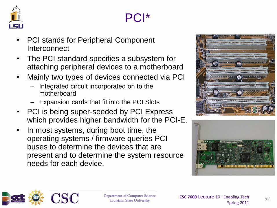
PCI*
• PCI stands for Peripheral Component Interconnect
• The PCI standard specifies a subsystem for attaching peripheral devices to a motherboard
• Mainly two types of devices connected via PCI– Integrated circuit incorporated on to the
motherboard
– Expansion cards that fit into the PCI Slots
• PCI is being super-seeded by PCI Express which provides higher bandwidth for the PCI-E.
• In most systems, during boot time, the operating systems / firmware queries PCI buses to determine the devices that are present and to determine the system resource needs for each device.
52

CSC 7600 Lecture 10 : Enabling TechSpring 2011
53
PCI enhanced systems
http://arstechnica.com/articles/paedia/hardware/pcie.ars/1
CSC 7600 Lecture 10 : Enabling TechSpring 2011
54
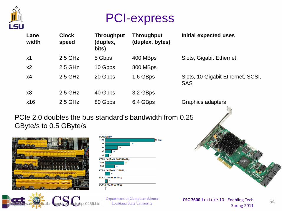
PCI-express
Lane
width
Clock
speed
Throughput
(duplex,
bits)
Throughput
(duplex, bytes)
Initial expected uses
x1 2.5 GHz 5 Gbps 400 MBps Slots, Gigabit Ethernet
x2 2.5 GHz 10 Gbps 800 MBps
x4 2.5 GHz 20 Gbps 1.6 GBps Slots, 10 Gigabit Ethernet, SCSI,
SAS
x8 2.5 GHz 40 Gbps 3.2 GBps
x16 2.5 GHz 80 Gbps 6.4 GBps Graphics adapters
http://www.redbooks.ibm.com/abstracts/tips0456.html
PCIe 2.0 doubles the bus standard's bandwidth from 0.25
GByte/s to 0.5 GByte/s
CSC 7600 Lecture 10 : Enabling TechSpring 2011
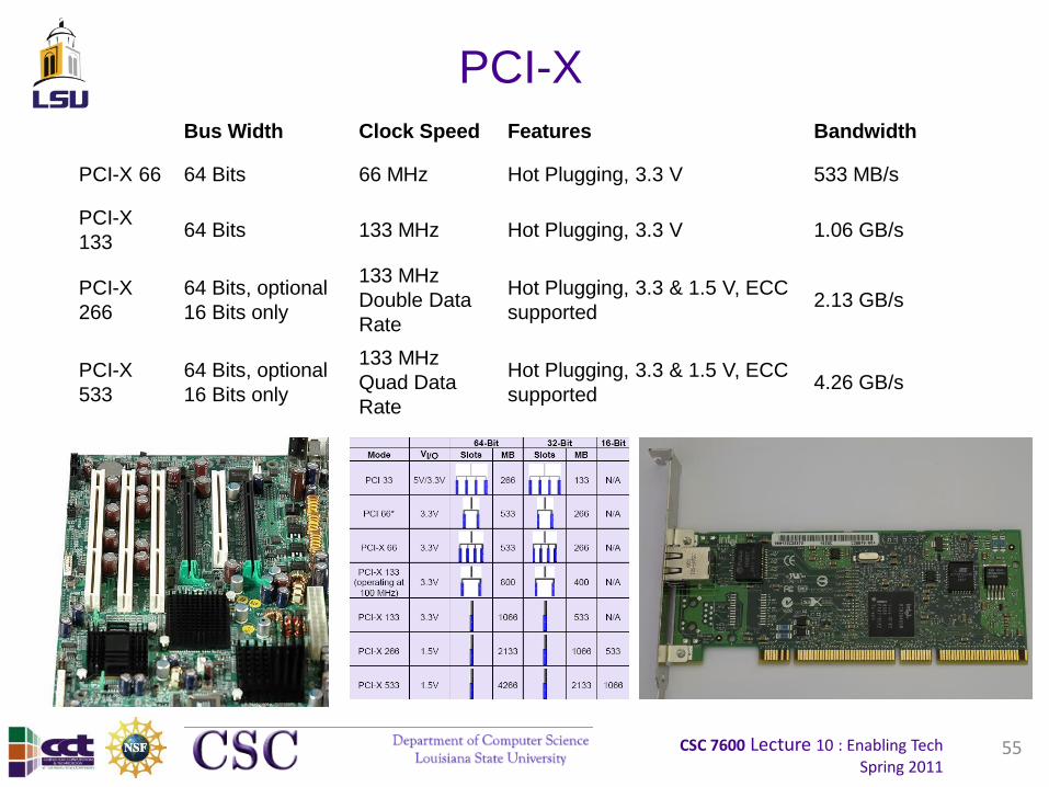
55
PCI-X
Bus Width Clock Speed Features Bandwidth
PCI-X 66 64 Bits 66 MHz Hot Plugging, 3.3 V 533 MB/s
PCI-X
13364 Bits 133 MHz Hot Plugging, 3.3 V 1.06 GB/s
PCI-X
266
64 Bits, optional
16 Bits only
133 MHz
Double Data
Rate
Hot Plugging, 3.3 & 1.5 V, ECC
supported2.13 GB/s
PCI-X
533
64 Bits, optional
16 Bits only
133 MHz
Quad Data
Rate
Hot Plugging, 3.3 & 1.5 V, ECC
supported4.26 GB/s

CSC 7600 Lecture 10 : Enabling TechSpring 2011
56
Bandwidth ComparisonsCONNECTION BITS BYTES
PCI 32-bit/33 MHz 1.06666 Gbit/s 133.33 MB/s
PCI 64-bit/33 MHz 2.13333 Gbit/s 266.66 MB/s
PCI 32-bit/66 MHz 2.13333 Gbit/s 266.66 MB/s
PCI 64-bit/66 MHz 4.26666 Gbit/s 533.33 MB/s
PCI 64-bit/100 MHz 6.39999 Gbit/s 799.99 MB/s
PCI Express (x1 link)[6] 2.5 Gbit/s 250 MB/s
PCI Express (x4 link)[6] 10 Gbit/s 1 GB/s
PCI Express (x8 link)[6] 20 Gbit/s 2 GB/s
PCI Express (x16 link)[6] 40 Gbit/s 4 GB/s
PCI Express 2.0 (x32 link)[6] 80 Gbit/s 8 GB/s
PCI-X DDR 16-bit 4.26666 Gbit/s 533.33 MB/s
PCI-X 133 8.53333 Gbit/s 1.06666 GB/s
PCI-X QDR 16-bit 8.53333 Gbit/s 1.06666 GB/s
PCI-X DDR 17.066 Gbit/s 2.133 GB/s
PCI-X QDR 34.133 Gbit/s 4.266 GB/s
AGP 8x 17.066 Gbit/s 2.133 GB/s
CSC 7600 Lecture 10 : Enabling TechSpring 2011
57
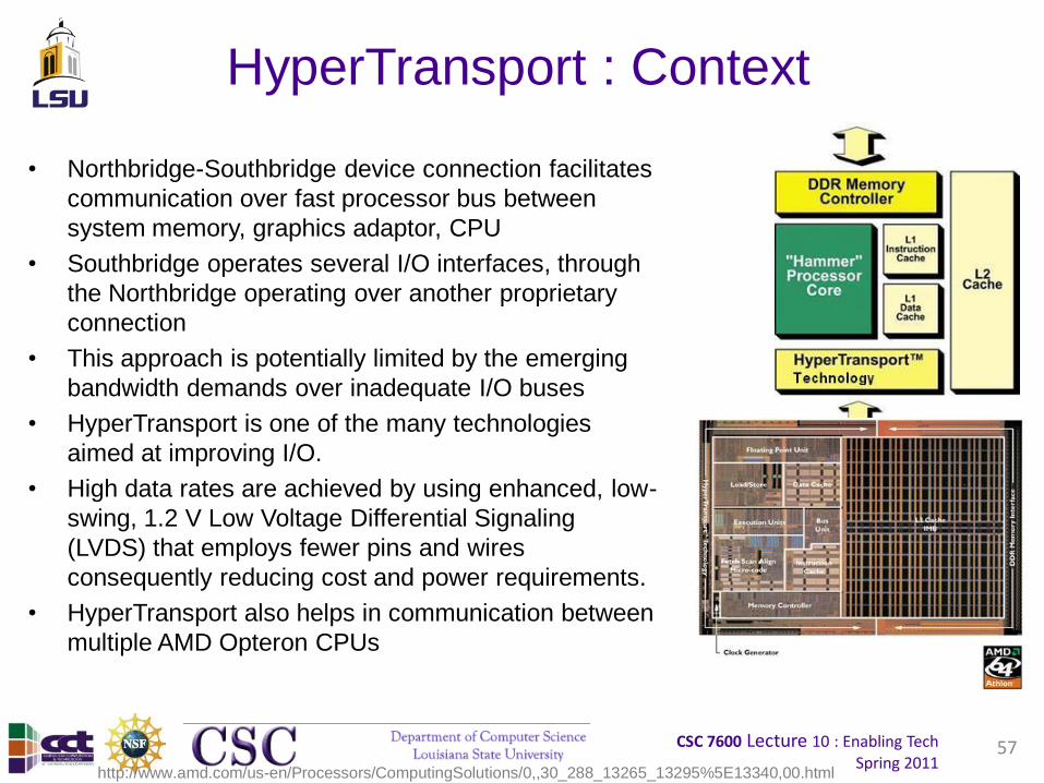
HyperTransport : Context
• Northbridge-Southbridge device connection facilitates
communication over fast processor bus between
system memory, graphics adaptor, CPU
• Southbridge operates several I/O interfaces, through
the Northbridge operating over another proprietary
connection
• This approach is potentially limited by the emerging
bandwidth demands over inadequate I/O buses
• HyperTransport is one of the many technologies
aimed at improving I/O.
• High data rates are achieved by using enhanced, low-
swing, 1.2 V Low Voltage Differential Signaling
(LVDS) that employs fewer pins and wires
consequently reducing cost and power requirements.
• HyperTransport also helps in communication between
multiple AMD Opteron CPUs
http://www.amd.com/us-en/Processors/ComputingSolutions/0,,30_288_13265_13295%5E13340,00.html

CSC 7600 Lecture 10 : Enabling TechSpring 2011
58
Hyper-Transport (continued)
• Point-to-point parallel topology uses 2
unidirectional links (one each for upstream and
downstream)
• HyperTransport technology chunks data into
packets to reduce overhead and improve efficiency
of transfers
• Each HyperTransport technology link also contains
8-bit data path that allows for insertion of a control
packet in the middle of a long data packet, thus
reducing latenc
• In Summary : “HyperTransport™ technology
delivers the raw throughput and low latency
necessary for chip-to-chip communication. It
increases I/O bandwidth, cuts down the number of
different system buses, reduces power
consumption, provides a flexible, modular bridge
architecture, and ensures compatibility with PCI.” http://www.amd.com/us-en/Processors/ComputingSolutions
/0,,30_288_13265_13295%5E13340,00.html

CSC 7600 Lecture 10 : Enabling TechSpring 2011
Topics
• Enabling Technologies - Introduction
• Processing Logic - CPU
• Memory Technology
• Communication - Concepts
• Intranode Communication (PCI, HT)
• Networking – Concepts
• Internode Communication (Ethernet, InfiniBand)
• Summary Materials for Test
59

CSC 7600 Lecture 10 : Enabling TechSpring 2011
Networking : A Historical Perspective
• Early machines were:
– Collection of microprocessors.
– Communication was performed using bi-directional queues
between nearest neighbors.
• Messages were forwarded by processors on path.
– “Store and forward” networking
• There was a strong emphasis on topology in algorithms, in
order to minimize the number of hops = minimize time
www.mat.unimi.it/users/pavarino/par_comp/
60
CSC 7600 Lecture 10 : Enabling TechSpring 2011
Network Analogy
• To have a large number of transfers occurring at once, you
need a large number of distinct wires.
• Networks are like streets:
– Link = street.
– Switch = intersection.
– Distances (hops) = number of blocks traveled.
– Routing algorithm = travel plan.
• Properties:
– Latency: how long to get between nodes in the network.
– Bandwidth: how much data can be moved per unit time.
• Bandwidth is limited by the number of wires and the rate at
which each wire can accept data.
www.mat.unimi.it/users/pavarino/par_comp/
61

CSC 7600 Lecture 10 : Enabling TechSpring 2011
InterNode Communication (OSI Model)*
• Open Systems Interconnect reference model (OSI Model)– Application Layer
• Interfaces directly to and performs application services for the application processes.
– Presentation Layer• Establishes a context between application layer entities
– Session Layer• Establishes, manages and terminates connections
– Transport Layer• Provides transparent transfer of data between end users,
TCP, UDP and other protocol layers
– Network Layer• Provides functional and procedural means of transferring
data from source to destination via one or more networks while maintaining the transport layer. eg. IP layer
– Data Link Layer• Provides the functional and procedural means to transfer
data between network entities and detect and correct errors in physical layers
– Physical Layer• Hubs, switches, cables etc
62
CSC 7600 Lecture 10 : Enabling TechSpring 2011
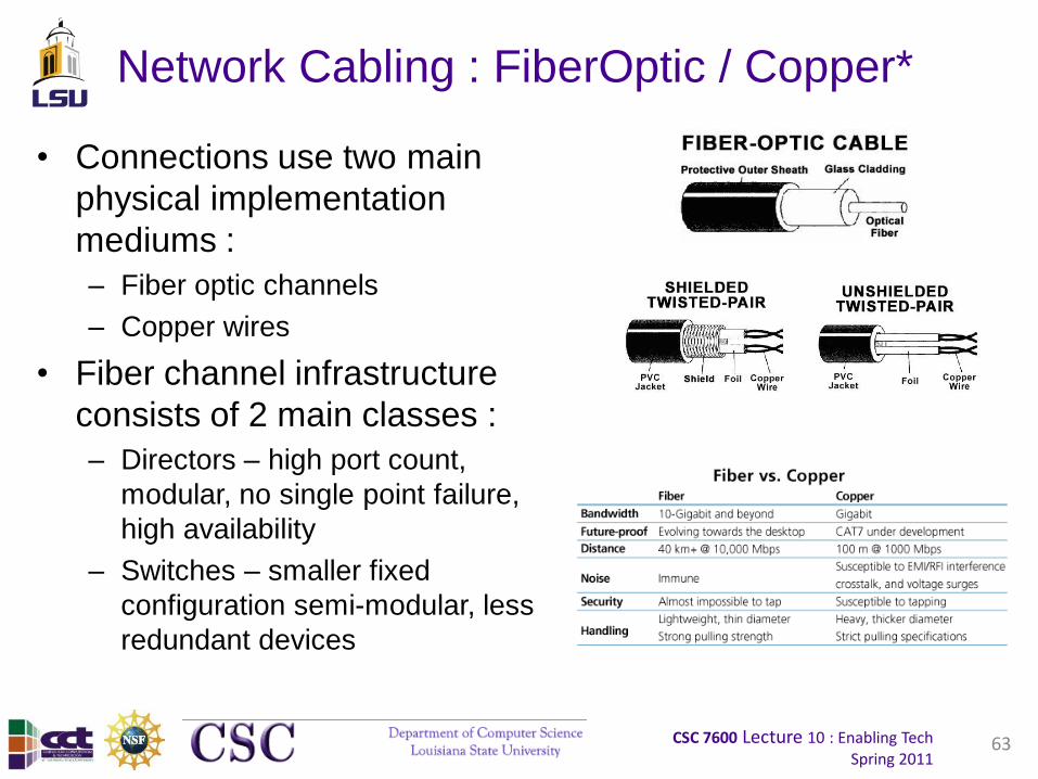
Network Cabling : FiberOptic / Copper*
• Connections use two main
physical implementation
mediums :
– Fiber optic channels
– Copper wires
• Fiber channel infrastructure
consists of 2 main classes :
– Directors – high port count,
modular, no single point failure,
high availability
– Switches – smaller fixed
configuration semi-modular, less
redundant devices
63

CSC 7600 Lecture 10 : Enabling TechSpring 2011
Design Characteristics of a Network*• Topology (how things are connected):
– Crossbar, ring, 2-D and 3-D meshes or torus, hypercube, tree, butterfly, perfect shuffle ....
• Routing algorithm (path used):
– Example in 2D torus: all east-west then all north-south (avoids deadlock).
• Switching strategy:
– Circuit switching: full path reserved for entire message, like the telephone.
– Packet switching: message broken into separately-routed packets, like the post office.
• Flow control (what if there is congestion):
– Stall, store data temporarily in buffers, re-route data to other nodes, tell source node to temporarily halt, discard, etc.
www.mat.unimi.it/users/pavarino/par_comp/
64

CSC 7600 Lecture 10 : Enabling TechSpring 2011
Performance Properties of a Network: Latency*
• Diameter: the maximum (over all pairs of nodes) of the shortest path between a given pair of nodes.
• Latency: delay between send and receive times
– Latency tends to vary widely across architectures
– Vendors often report hardware latencies (wire time)
– Application programmers care about software latencies (user program to user program)
• Observations:
– Hardware/software latencies often differ by 1-2 orders of magnitude
– Maximum hardware latency varies with diameter, but the variation in software latency is usually negligible
• Latency is important for programs with many small messages www.mat.unimi.it/users/pavarino/par_comp/
65
CSC 7600 Lecture 10 : Enabling TechSpring 2011
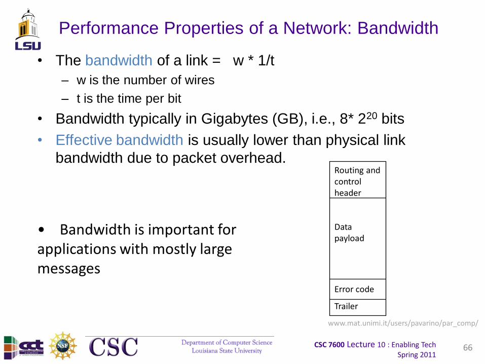
Performance Properties of a Network: Bandwidth
• The bandwidth of a link = w * 1/t
– w is the number of wires
– t is the time per bit
• Bandwidth typically in Gigabytes (GB), i.e., 8* 220 bits
• Effective bandwidth is usually lower than physical link
bandwidth due to packet overhead.Routing and control header
Data payload
Error code
Trailer
• Bandwidth is important for applications with mostly large messages
www.mat.unimi.it/users/pavarino/par_comp/
66
CSC 7600 Lecture 10 : Enabling TechSpring 2011
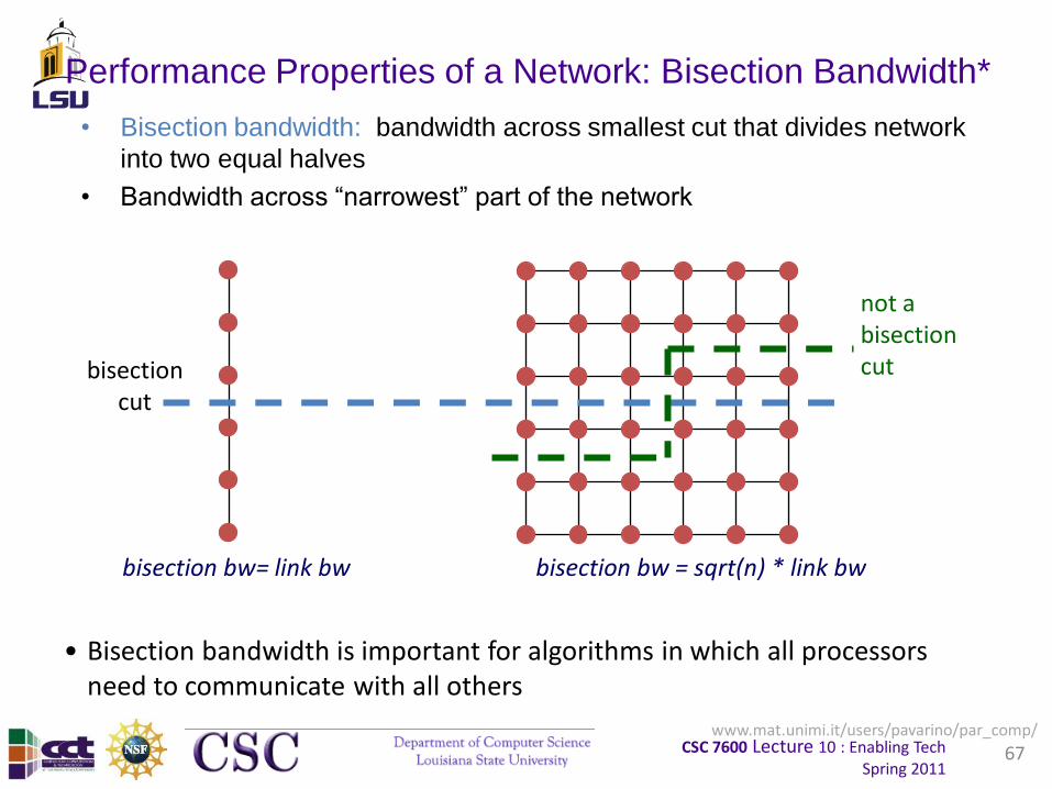
Performance Properties of a Network: Bisection Bandwidth*
• Bisection bandwidth: bandwidth across smallest cut that divides network
into two equal halves
• Bandwidth across “narrowest” part of the network
bisection cut
not a bisectioncut
bisection bw= link bw bisection bw = sqrt(n) * link bw
• Bisection bandwidth is important for algorithms in which all processors need to communicate with all others
www.mat.unimi.it/users/pavarino/par_comp/
67

CSC 7600 Lecture 10 : Enabling TechSpring 2011
Network Topology
• In the past, there was considerable research in network topology and in mapping algorithms to topology.
– Key cost to be minimized: number of “hops” between nodes (e.g. “store and forward”)
– Modern networks hide hop cost (i.e., “wormhole routing”), so topology is no longer a major factor in algorithm performance.
• Example: On IBM SP system, hardware latency varies from 0.5 usec to 1.5 usec, but user-level message passing latency is roughly 36 usec.
• Need some background in network topology
– Algorithms may have a communication topology
– Topology affects bisection bandwidth.
www.mat.unimi.it/users/pavarino/par_comp/
68
CSC 7600 Lecture 10 : Enabling TechSpring 2011
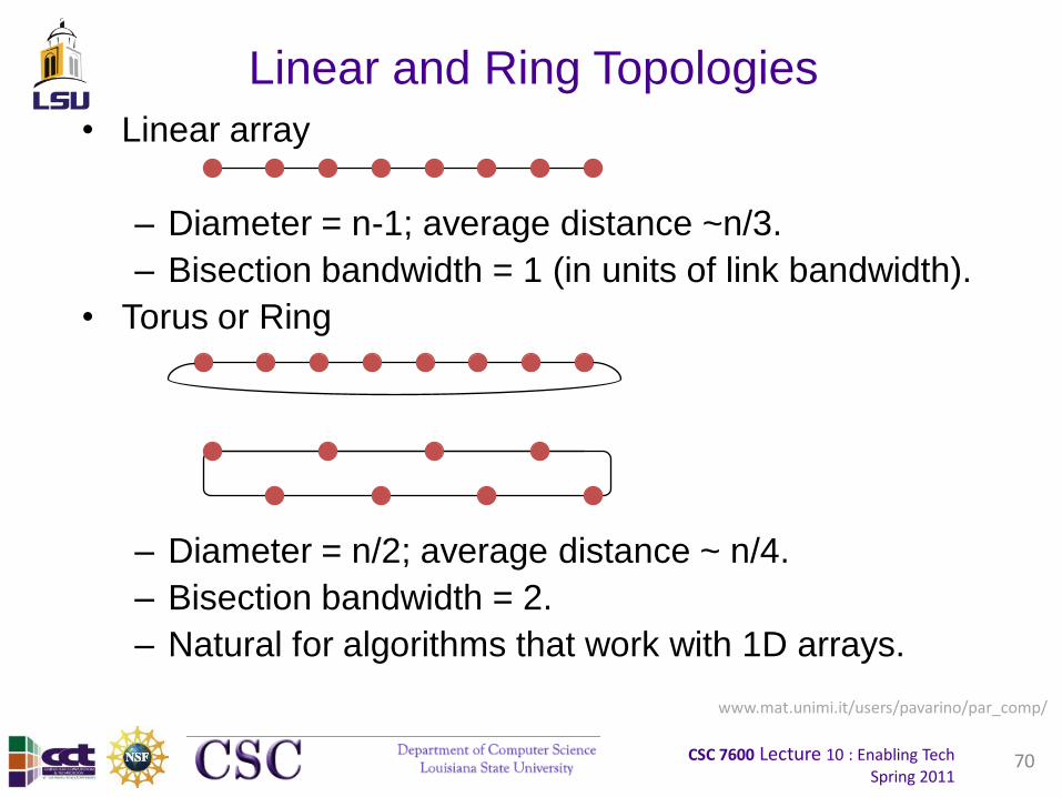
Linear and Ring Topologies
• Linear array
– Diameter = n-1; average distance ~n/3.
– Bisection bandwidth = 1 (in units of link bandwidth).
• Torus or Ring
– Diameter = n/2; average distance ~ n/4.
– Bisection bandwidth = 2.
– Natural for algorithms that work with 1D arrays.
www.mat.unimi.it/users/pavarino/par_comp/
70

CSC 7600 Lecture 10 : Enabling TechSpring 2011
Meshes and Toroids*
Two dimensional mesh
– Diameter = 2 * (sqrt(n ) – 1)
– Bisection bandwidth = sqrt(n)
• Generalizes to higher dimensions (Cray T3D used 3D Torus).
• Natural for algorithms that work with 2D and/or 3D arrays.
Two dimensional torus
• Diameter = sqrt(n )
• Bisection bandwidth = 2* sqrt(n)
www.mat.unimi.it/users/pavarino/par_comp/
71
CSC 7600 Lecture 10 : Enabling TechSpring 2011
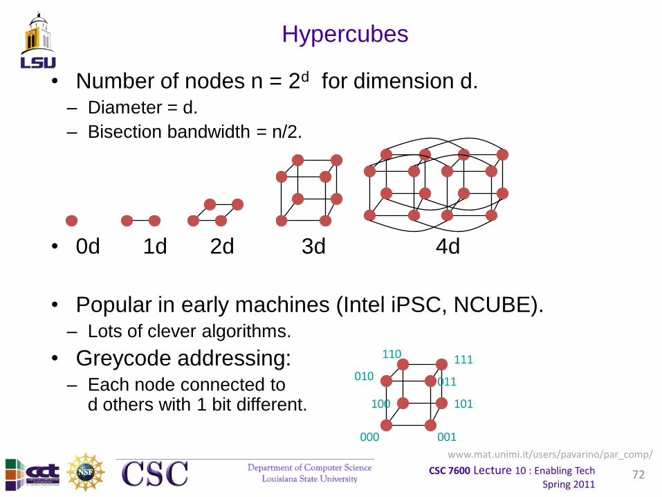
Hypercubes
• Number of nodes n = 2d for dimension d.– Diameter = d.
– Bisection bandwidth = n/2.
• 0d 1d 2d 3d 4d
• Popular in early machines (Intel iPSC, NCUBE).– Lots of clever algorithms.
• Greycode addressing:– Each node connected to
d others with 1 bit different.
001000
100
010 011
111
101
110
www.mat.unimi.it/users/pavarino/par_comp/
72

CSC 7600 Lecture 10 : Enabling TechSpring 2011
Trees*• Diameter = log n.
• Bisection bandwidth = 1.
• Easy layout as planar graph.
• Many tree algorithms (e.g., summation).
• Fat trees avoid bisection bandwidth problem:
– More (or wider) links near top.
– Example: Thinking Machines CM-5.
www.mat.unimi.it/users/pavarino/par_comp/
73

CSC 7600 Lecture 10 : Enabling TechSpring 2011
Butterflies with n = (k+1)2^k nodes
• Diameter = 2k.
• Bisection bandwidth = 2^k.
• Cost: lots of wires.
• Used in BBN Butterfly.
• Natural for FFT.
O 1O 1
O 1 O 1
butterfly switch
multistage butterfly network
www.mat.unimi.it/users/pavarino/par_comp/
74

CSC 7600 Lecture 10 : Enabling TechSpring 2011
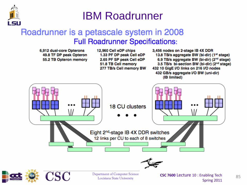
Topologies in Real Machines
Road Runner Fat tree
Red Storm (Opteron + Cray network, future)
3D Mesh
Blue Gene/L & Blue Gene /P 3D Torus
SGI Altix Fat tree
Cray X1 4D Hypercube*
Myricom (Millennium) Arbitrary
Quadrics (in HP Alpha server clusters)
Fat tree
IBM SP Fat tree (approx)
SGI Origin Hypercube
Intel Paragon (old) 2D Mesh
BBN Butterfly (really old) Butterfly
old
er
new
er
Many of these are approximations:E.g., the X1 is really a “quad bristled hypercube” and some of the fat trees are not as fat as they should be at the top
www.mat.unimi.it/users/pavarino/par_comp/
75
CSC 7600 Lecture 10 : Enabling TechSpring 2011
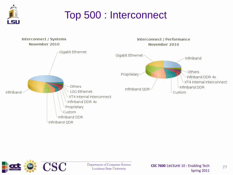
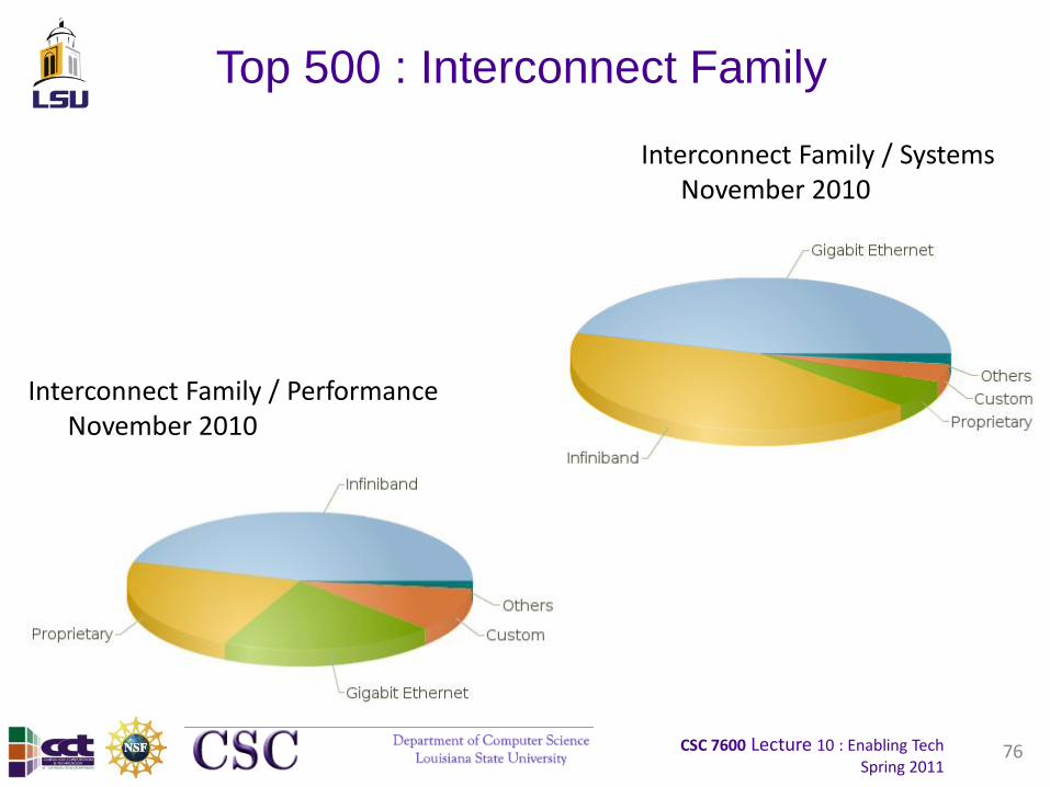
Top 500 : Interconnect Family
76
Interconnect Family / Systems November 2010
Interconnect Family / Performance November 2010

CSC 7600 Lecture 10 : Enabling TechSpring 2011
Topics
• Enabling Technologies - Introduction
• Processing Logic - CPU
• Memory Technology
• Communication - Concepts
• Intranode Communication (PCI, HT)
• Networking – Concepts
• Internode Communication (Ethernet, InfiniBand)
• Summary Materials for Test
78

CSC 7600 Lecture 10 : Enabling TechSpring 2011
Ethernet
This diagram was hand drawn by Robert M.
Metcalfe and photographed by Dave R.
Boggs in 1976 to produce a 35mm slide
used to present Ethernet to the National
Computer Conference in June1976
79

CSC 7600 Lecture 10 : Enabling TechSpring 2011
Ethernet – Cards / Controllers*
• Gigabit Ethernet
– Approximate speed of 1000 Mbits/s
– Transmission range 5 km
– IEEE 802.3 standard
– Some times integrated with the mother board
– PCI based extension cards available
– Common chipset manufacturers: Broadcom,
intel, Cisco, D-Link, 3com etc
• 10 Gigabit Ethernet
– Approximate speed of 10 Gbits/s
– Transmission range 40 km
– Works with IEEE 802.3 standard
– PCIe / PCIx based cards available
– Common chipset manufacturers include intel
80
Gigabit Ethernet PCI Card
10 Gigabit Ethernet PCIX Card
Dual-port Multithreaded 10 Gigabit Ethernet PCIe Card

CSC 7600 Lecture 10 : Enabling TechSpring 2011
Ethernet Switches & Cables
• Networking device that operates at any of the OSI layers, physical, datalink, network or transport. (Multilayer switch, one that operates at several OSI layers)
• Switch ports almost always default to full-duplex operation, unless there is a requirement for interoperability with devices that are strictly half duplex
• Half-duplex means that the device can only send or receive at any given time, whereas full-duplex can send and receive at the same time
• Switches come in several form factor: rack mounted, non-rack mounted, chassis
• Managed or Unmanaged switching– Unmanaged switches do not have
configuration interface or options
– Managed switches allow access to one or more interfaces for maintenance and management
81
10 GigE Switch
1 GigE Switch
Chassis Switch

CSC 7600 Lecture 10 : Enabling TechSpring 2011
InfiniBand Switches and HCAs*
• InfiniBand is a point-to-point bidirectional serial link intended for the connection of processors with high speed peripherals such as disks.
• It supports several signaling rates and, as with PCIe, links can be channel bonded together for additional bandwidth.
• The serial connection's signaling rate is 2.5 Gbits/s in each direction per connection.
• InfiniBand supports double (DDR – 5Gbits/s) and quad data (QDR –10Gbits/s) speeds, at the same data-clock rate.
• The single data rate switch chips have a latency of 200ns, and DDR switch chips have a latency of 140ns
• InfiniBand uses a switched fabric topology, as opposed to a hierarchical switched network like Ethernet.
• Data is transmitted in packets of up to 4 kB that are taken together to form a message. A message can be:
– a direct memory access read from or, write to, a remote node (RDMA)– a channel send or receive– a transaction-based operation (that can be reversed)– a multicast transmission.– An atomic operation
82

CSC 7600 Lecture 10 : Enabling TechSpring 2011
InfiniBand Cabling
• CX4 Copper (15m)
• Flexible 30-Gauge Copper (3m)
• Fiber Optics up to 150m
83
Effective theoretical throughput in different configurations Single Double Quad
1X 2 Gbit/s 4 Gbit/s 8 Gbit/s4X 8 Gbit/s 16 Gbit/s 32 Gbit/s12X 24 Gbit/s 48 Gbit/s 96 Gbit/s

CSC 7600 Lecture 10 : Enabling TechSpring 2011
520 Dual CPU Nodes1,040 CPUs
NCSANational Center for Supercomputing Applications
Tungsten 2: 520 Node Supercomputer
Core Fabric
Edge Fabric
6 72-portTS270
29 24-portTS120
174 uplinkcables
512 1mcables
18 Compute Nodes
18 Compute Nodes
Parallel MPI codes for commercial clients
Point to point 5.2us MPI latency
Deployed: November 2004
84

CSC 7600 Lecture 10 : Enabling TechSpring 2011
InfiniBand Price / Performance
InfiniBandPCI-Express
10GigE GigE Myrinet D Myrinet E
Data Bandwidth(Large Messages)
950MB/s 900MB/s 100MB/s 245MB/s 495MB/s
MPI Latency(Small Messages)
5us 50us 50us 6.5us 5.7us
HCA Cost(Street Price)
$550 $1.5K Free $535 $880
Switch Port $250 $1K-$2K $100-$300 $400 $400
Cable Cost(3m Street Price)
$100 $100 $25 $175 $175
•Myrinet pricing data from Myricom Web Site (Dec 2004) ** InfiniBand pricing data based on Topspin avg. sales price (Dec 2004)*** Myrinet, GigE, and IB performance data from June 2004 OSU study
• Note: MPI Processor to Processor latency – switch latency is less
86

CSC 7600 Lecture 10 : Enabling TechSpring 2011
The InfiniBand Driver Architecture
BSD Sockets FS API
TCP
SDP
IP
DriversVERBS
ETHER INFINIBAND HCA
DAT
FILE SYSTEM
SCSI
SRP
FC
FCP
SDP
INFINIBAND SAN
API
BSD Sockets NFS-RDMA
LAN/WAN SERVER FABRICSAN
INFINIBAND SWITCHETHER
SWITCHFC
SWITCHFC GWEETH GW
NETWORK
APPLICATION
UDAPL
TS TS
IPoIB
User
Kernel
87

CSC 7600 Lecture 10 : Enabling TechSpring 2011
Topics
• Enabling Technologies - Introduction
• Processing Logic - CPU
• Memory Technology
• Communication - Concepts
• Intranode Communication (PCI, HT)
• Networking – Concepts
• Internode Communication (Ethernet, InfiniBand)
• Summary Materials for Test
88

CSC 7600 Lecture 10 : Enabling TechSpring 2011
89
Summary – Material for the Test
• Logic technology & metrics – 12• Memory technology & metrics – 23• Main memory implementation – 25• Static and Dynamic RAM – 26,28• Current SDRAM variants – 29,30• Flash memory – 35• Secondary Storage hard drives – 38• Communication concepts – 42• Ways to transfer data from memory & devices – 47• Northbridge & Southbridge – 51• PCI technology - 52• OSI model – 62• Cabling technologies: Fiber vs Cu - 63• Design characteristics – 64• Performance properties of Network: Latency – 65• Bisection bandwidth – 67• Network topologies: Mesh & Toroids – 71• Network topologies: Tree – 73• Ethernet Cards/Controller – 80• IB switch & HCA – 82