Monolithic fully depleted CMOS sensors for frontier vertex ...
High Luminosity ATLAS vs. CMOS SensorsWhere we currently are and
where we’d like to be
Jens Dopke, STFC RAL
1

Disclaimer I usually do talks on things where I generated all
the imagery myself (ATLAS Pixels/IBL) - CMOS
as a topic was a particular wish and I’ll give
some insights, but much of it will rely on you
asking questions (and quite possibly people in
the audience knowing better answering them…)
Many images “stolen” from others, all of it is
collaborative effort...
2
Outline ● Introduction
○ What do we do now
○ ATLAS ITk in the making
○ What can we do different?
● Technology
○ How would we do it
○ What exists
● Status
○ Are we there yet?
● Summary++
3
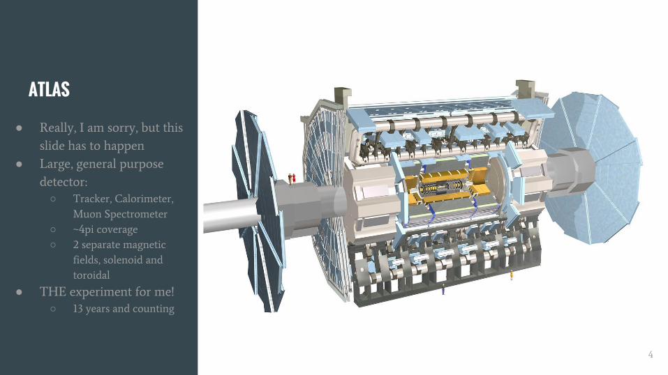
ATLAS
● Really, I am sorry, but this
slide has to happen
● Large, general purpose
detector:
○ Tracker, Calorimeter,
Muon Spectrometer
○ ~4pi coverage
○ 2 separate magnetic
fields, solenoid and
toroidal
● THE experiment for me!
○ 13 years and counting
4

ATLAS Tracker
● 3 individual Systems:
○ TRT: Gaseous detector
with transition radiation
○ Stried semiconductor
○ Pixelised semiconductor
● Spatial resolution:
○ D0 ~ 10um
○ Z0 ~ 50um
● Certain Features:
○ Unmaintainable (Well...)
○ Power consumption
(Mostly in delivery)
○ Cooling (For now based
on C3F8)
5
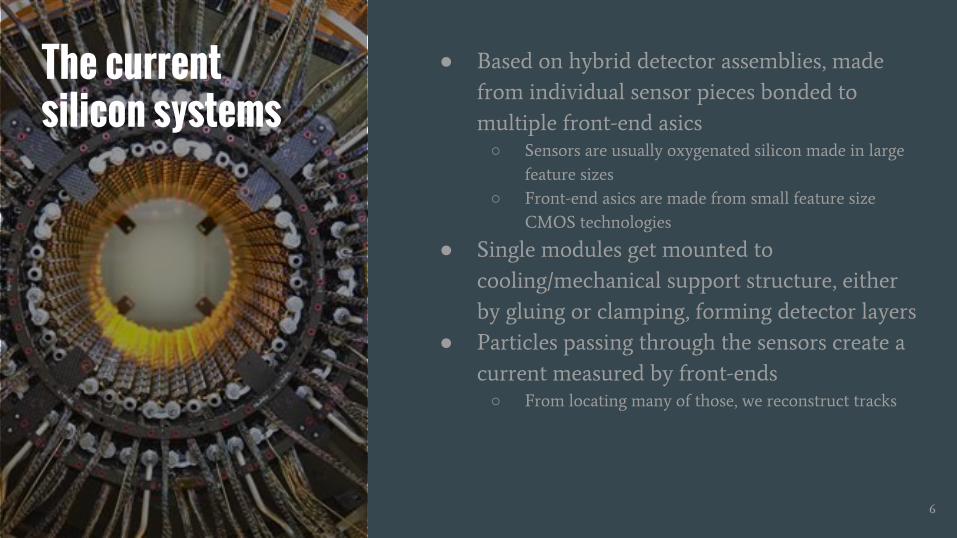
The current silicon systems
● Based on hybrid detector assemblies, made
from individual sensor pieces bonded to
multiple front-end asics
○ Sensors are usually oxygenated silicon made in large
feature sizes
○ Front-end asics are made from small feature size
CMOS technologies
● Single modules get mounted to
cooling/mechanical support structure, either
by gluing or clamping, forming detector layers
● Particles passing through the sensors create a
current measured by front-ends
○ From locating many of those, we reconstruct tracks
6
7
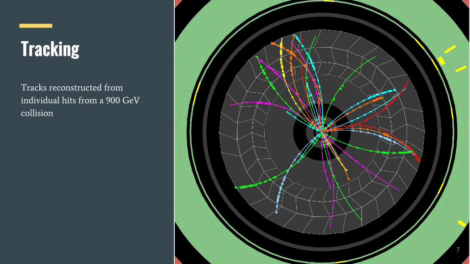
Tracking
Tracks reconstructed from
individual hits from a 900 GeV
collision
8
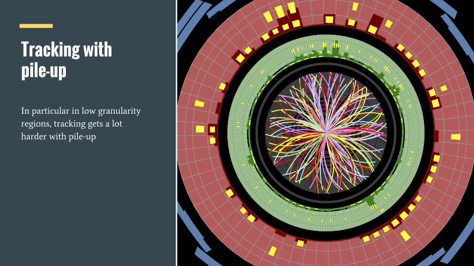
Tracking with pile-up
In particular in low granularity
regions, tracking gets a lot
harder with pile-up
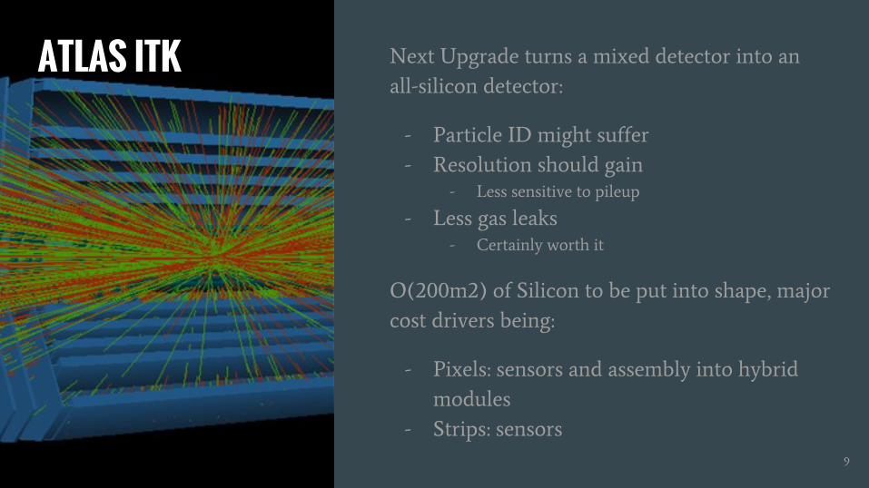
ATLAS ITK Next Upgrade turns a mixed detector into an
all-silicon detector:
- Particle ID might suffer
- Resolution should gain
- Less sensitive to pileup
- Less gas leaks
- Certainly worth it
O(200m2) of Silicon to be put into shape, major
cost drivers being:
- Pixels: sensors and assembly into hybrid
modules
- Strips: sensors
9
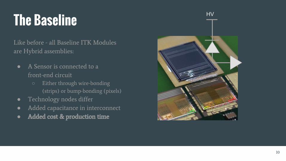
The BaselineLike before - all Baseline ITK Modules
are Hybrid assemblies:
● A Sensor is connected to a
front-end circuit
○ Either through wire-bonding
(strips) or bump-bonding (pixels)
● Technology nodes differ
● Added capacitance in interconnect
● Added cost & production time
HV
10
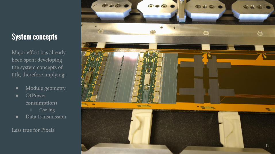
System concepts
Major effort has already
been spent developing
the system concepts of
ITk, therefore implying:
● Module geometry
● O(Power
consumption)
○ Cooling
● Data transmission
Less true for Pixels!
11
Intermediate SummaryITk as a project is quite well advanced:
● Strip TDR is being circulated to LHCC as we speak
● The number of possible Pixel system design choices decreases...
● Services are already being dissected to understand our future powering scheme
What Options does that still leave us with?
12
- - - - - - - - - - - - - - - - CUT here - - - - - - - - - - - - - - - - -
13
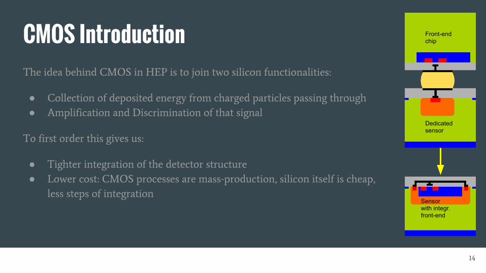
CMOS IntroductionThe idea behind CMOS in HEP is to join two silicon functionalities:
● Collection of deposited energy from charged particles passing through
● Amplification and Discrimination of that signal
To first order this gives us:
● Tighter integration of the detector structure
● Lower cost: CMOS processes are mass-production, silicon itself is cheap,
less steps of integration
Front-endchip
Dedicatedsensor
Sensorwith integr.front-end
14
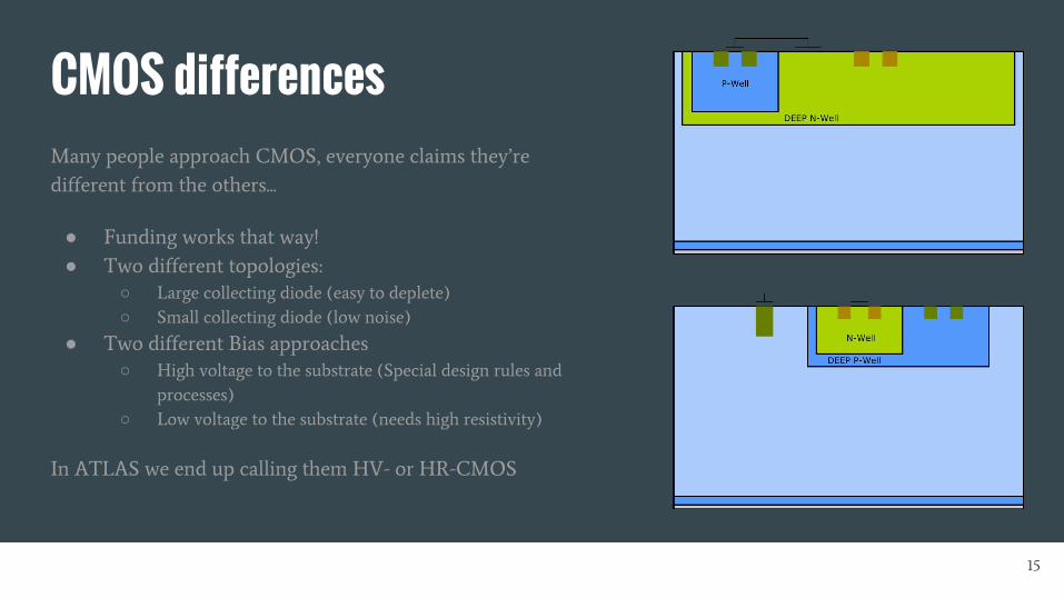
CMOS differencesMany people approach CMOS, everyone claims they’re
different from the others...
● Funding works that way!
● Two different topologies:
○ Large collecting diode (easy to deplete)
○ Small collecting diode (low noise)
● Two different Bias approaches
○ High voltage to the substrate (Special design rules and
processes)
○ Low voltage to the substrate (needs high resistivity)
In ATLAS we end up calling them HV- or HR-CMOS
15
CMOS - TechnologyAnother main aspect are technology differences - what do the fabs offer?
- Triple/Quadruple Well Architecture
- Epitaxial silicon
- HV design kits/rules
- Insulation between CMOS process and substrate (SOI)
Foundry list during investigation got a bit excessive, can now break it down to about
4 foundries that will deliver all of the above
- Feature size for all of these is usually between 350nm and 150nm
16
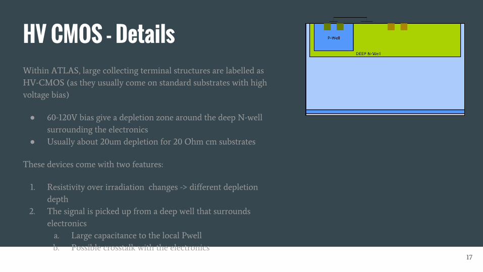
HV CMOS - DetailsWithin ATLAS, large collecting terminal structures are labelled as
HV-CMOS (as they usually come on standard substrates with high
voltage bias)
● 60-120V bias give a depletion zone around the deep N-well
surrounding the electronics
● Usually about 20um depletion for 20 Ohm cm substrates
These devices come with two features:
1. Resistivity over irradiation changes -> different depletion
depth
2. The signal is picked up from a deep well that surrounds
electronics
a. Large capacitance to the local Pwell
b. Possible crosstalk with the electronics
17
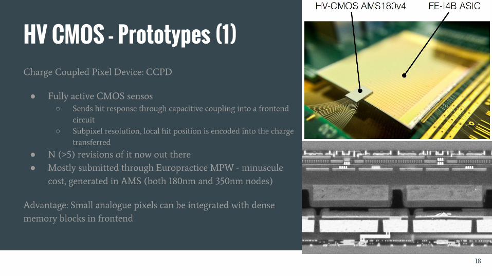
HV CMOS - Prototypes (1)Charge Coupled Pixel Device: CCPD
● Fully active CMOS sensos
○ Sends hit response through capacitive coupling into a frontend
circuit
○ Subpixel resolution, local hit position is encoded into the charge
transferred
● N (>5) revisions of it now out there
● Mostly submitted through Europractice MPW - minuscule
cost, generated in AMS (both 180nm and 350nm nodes)
Advantage: Small analogue pixels can be integrated with dense
memory blocks in frontend
18
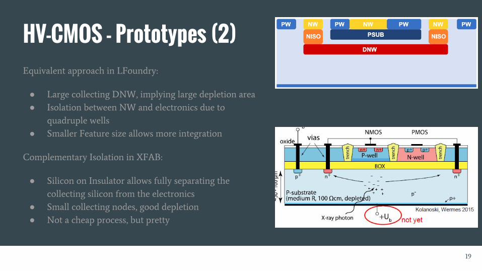
HV-CMOS - Prototypes (2)Equivalent approach in LFoundry:
● Large collecting DNW, implying large depletion area
● Isolation between NW and electronics due to
quadruple wells
● Smaller Feature size allows more integration
Complementary Isolation in XFAB:
● Silicon on Insulator allows fully separating the
collecting silicon from the electronics
● Small collecting nodes, good depletion
● Not a cheap process, but pretty
19
HV-CMOS ProductionMu3e experiment at PSI
● Needs minimal material:
○ 50um thinned CMOS sensors, based on AMS
180 HV
● Fully monolithic architecture, all hits read out
per bunch crossing
● Awesome detector concept with helium gas
cooling, which they’re now trying to market
for ATLAS
○ Only needs a factor of about 1000 more area...
20
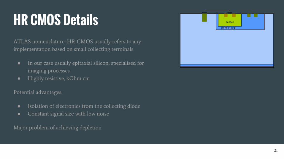
HR CMOS DetailsATLAS nomenclature: HR-CMOS usually refers to any
implementation based on small collecting terminals
● In our case usually epitaxial silicon, specialised for
imaging processes
● Highly resistive, kOhm cm
Potential advantages:
● Isolation of electronics from the collecting diode
● Constant signal size with low noise
Major problem of achieving depletion
21
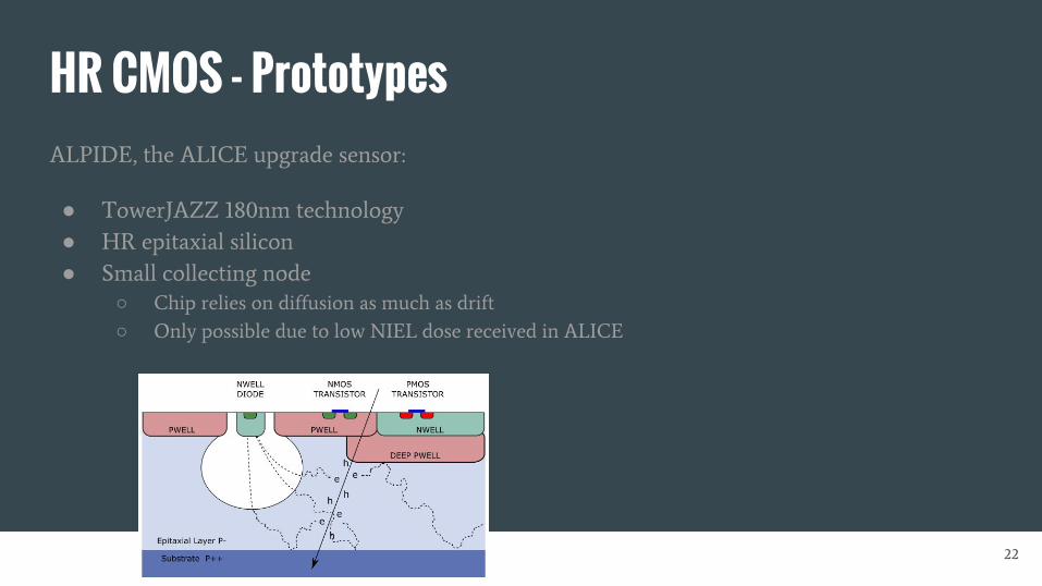
HR CMOS - PrototypesALPIDE, the ALICE upgrade sensor:
● TowerJAZZ 180nm technology
● HR epitaxial silicon
● Small collecting node
○ Chip relies on diffusion as much as drift
○ Only possible due to low NIEL dose received in ALICE
22
Now where is ATLAS?Two major projects within ATLAS:
● Program in CMOS strips: CHESS
● CMOS Pixel Demonstrator program
○ Now evolved into a MAPS program
○ Not really mine, haven’t looked at things here in a while...
Both aiming at a plug-in solution - time is too short to require significant
modification of mechanical/thermal supports
Given that we need a stable baseline, both projects are funded either through
individual funding requests, tapping into the upgrade project or being lucky...
23
CHESS Evaluation program for a strip-like implementation:
● Long(ish) pixels
● Low occupancy, but high peak density (jet cores)
● High resolution
Initial revision with very quick turnaround envisaged (program started mid 2014)
● Many pixelised test structures of different size
● Passive structures allowing more direct tests of the semiconductor behaviour
● Initial active pixel array set
24
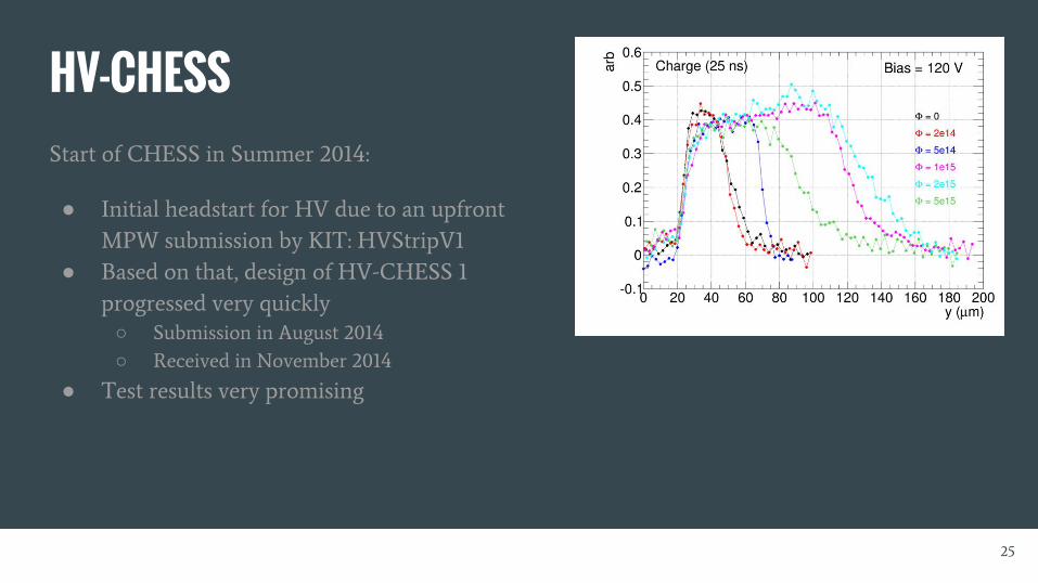
HV-CHESSStart of CHESS in Summer 2014:
● Initial headstart for HV due to an upfront
MPW submission by KIT: HVStripV1
● Based on that, design of HV-CHESS 1
progressed very quickly
○ Submission in August 2014
○ Received in November 2014
● Test results very promising
25
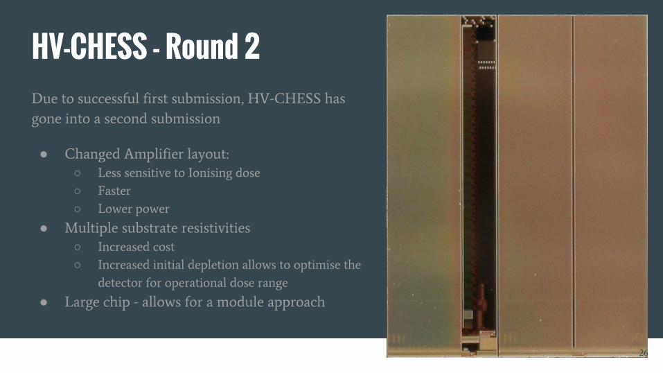
HV-CHESS - Round 2Due to successful first submission, HV-CHESS has
gone into a second submission
● Changed Amplifier layout:
○ Less sensitive to Ionising dose
○ Faster
○ Lower power
● Multiple substrate resistivities
○ Increased cost
○ Increased initial depletion allows to optimise the
detector for operational dose range
● Large chip - allows for a module approach
26
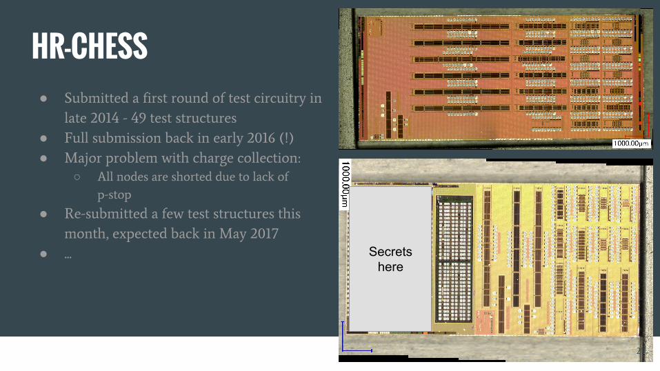
HR-CHESS● Submitted a first round of test circuitry in
late 2014 - 49 test structures
● Full submission back in early 2016 (!)
● Major problem with charge collection:
○ All nodes are shorted due to lack of
p-stop
● Re-submitted a few test structures this
month, expected back in May 2017
● ...Secrets
here
27
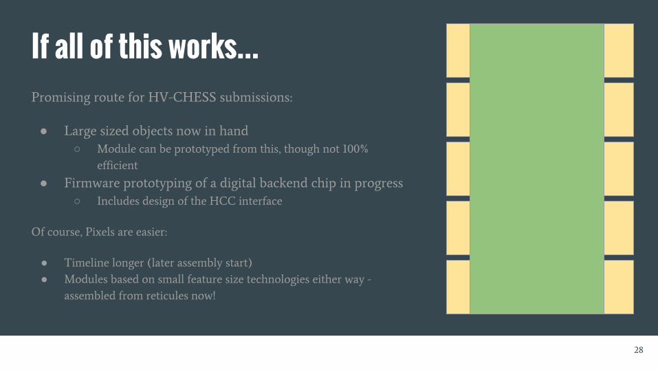
If all of this works...Promising route for HV-CHESS submissions:
● Large sized objects now in hand
○ Module can be prototyped from this, though not 100%
efficient
● Firmware prototyping of a digital backend chip in progress
○ Includes design of the HCC interface
Of course, Pixels are easier:
● Timeline longer (later assembly start)
● Modules based on small feature size technologies either way -
assembled from reticules now!
28
ConclusionsMany CMOS implementations coming up in HEP:
● Mu3e
● ALICE
● STAR
● BELLE
CMOS is really getting somewhere, in particular in terms of radiation hardness
● Too late for ATLAS ITk Strips it would seem
● ATLAS ITk Pixels following through with an attempt to a monolithic
implementation for the outermost pixel layer
29

ReferencesStarted collecting but didn’t get very far...
https://arxiv.org/pdf/1509.09052.pdf
30