High Frequency Measurement Device - · PDF fileHigh Frequency Measurement Device ... power...
30
High Frequency Measurement Device Senior Design Report Spring Semester 2007 By Stephanie Auyoung Derek Hall Eric Hall Joel Stanczyk Kevin Todd Prepared to partially fulfill the requirements for EE402/EE401 Department of Electrical and Computer Engineering Colorado State University Fort Collins, Colorado 80523 Report Approved: _______________________________________ Project Advisor _______________________________________ Senior Design Coordinator
Transcript of High Frequency Measurement Device - · PDF fileHigh Frequency Measurement Device ... power...

High Frequency Measurement Device
Senior Design Report Spring Semester 2007
By Stephanie Auyoung
Derek Hall Eric Hall
Joel Stanczyk Kevin Todd
Prepared to partially fulfill the requirements for EE402/EE401
Department of Electrical and Computer Engineering Colorado State University
Fort Collins, Colorado 80523
Report Approved: _______________________________________ Project Advisor _______________________________________ Senior Design Coordinator
ii
ABSTRACT The HFM team was charged with the task of building a high frequency measuring device capable
of measuring the power characteristics of high power RF circuits. The need for such a device is
due to the lack of features and the prohibitive expense of similar commercially available devices.
The HFM team’s goal was to create a less expensive, compact, and practical device capable of
performing the required tasks.
Initial requirements for the device included measuring voltage and current as well as the phase
between them and then to output such information to a computer. These measurements are
needed to find the reflection coefficient which is critical in impedance matching for RF circuits.
An unmatched circuit leads to a standing wave on the transmission line which reduces power
transfer efficiency and may lead to circuit damage. The HFM team was presented with three
components to be used in the implementation of the HFM device. These components are the
AD8302 from Analog Devices, the ADL5310 also from Analog Devices, and the PSoC mixed-
signal controller from the Cypress Semiconductor Corporation. The AD8302 has superior
voltage and phase measurement capabilities while the ADL5310 had unmatched current analysis
abilities however it was discovered that by using a directional coupler one can effectively get the
reflection coefficient only using the AD8302. The PSoC was chosen based on its signal
processing capabilities and the relative ease of USB interface implementation to aid in the final
product’s GUI computer interface.

iii
TABLE OF CONTENTS
High Frequency Measurement Device ________________________________________ i
ABSTRACT _____________________________________________________________________ ii
TABLE OF CONTENTS ___________________________________________________________ iii
LIST OF FIGURES AND TABLES __________________________________________________iv
Chapter I – Introduction ___________________________________________________________ 1
Chapter II – Summary of Previous Work _____________________________________________ 3
Chapter III – Device Design ________________________________________________________ 4 Components___________________________________________________________________________ 4 High Power Accommodations_____________________________________________________________ 5 Figure 1: Reflection Coefficient____________________________________________________________ 6 PSoC_________________________________________________________________________________ 7 Computer GUI__________________________________________________________________________ 8 Figure 2: HFM GUI Flowchart____________________________________________________________ 9 Budget_______________________________________________________________________________ 10
Chapter IV – Conclusions & Continuation ___________________________________________ 11 Conclusions:__________________________________________________________________________ 11 Possible Project Continuations:____________________________________________________________ 12
ACKNOWLEDGEMENTS ________________________________________________________ 14
REFERENCES__________________________________________________________________ 15
BIBLIOGRAPHY ________________________________________________________________ 16
APPENDIX _______________________________________________________________________I Figures and Tables_______________________________________________________________________ I Figure 3: CY8C24794 PSoC Functional Block Diagram [2] _______________________________________ I Figure 4: AD8302 Functional Block Diagram [3]_______________________________________________II Figure 5: ADL5310 Functional Block Diagram [4]______________________________________________II Figure 6: CY8C24794 56-Pin PSoC Device [1]_______________________________________________ III Table 1: Pin Function Descriptions [1]______________________________________________________ III Figure 7: AD8302 14-Pin Configuration [3]__________________________________________________ V Table 2: Pin Function Descriptions_________________________________________________________VI Figure 8: AD8302 Equivalent Circuits [3]___________________________________________________ VII Figure 9: ADL5310 24-Lead LFCS Pin Configuration [4] ______________________________________VIII Table 3: Pin Function Descriptions_________________________________________________________ IX Individual Project Roles__________________________________________________________________ X

iv
LIST OF FIGURES AND TABLES Figure 1: Reflection Coefficient____________________________________________________________ 6 Figure 2: HFM GUI Flowchart____________________________________________________________ 9 Figure 3: CY8C24794 PSoC Functional Block Diagram [2] _______________________________________ I Figure 4: AD8302 Functional Block Diagram [3]_______________________________________________II Figure 5: ADL5310 Functional Block Diagram [4]______________________________________________II Figure 6: CY8C24794 56-Pin PSoC Device [1]_______________________________________________ III Figure 7: AD8302 14-Pin Configuration [3]__________________________________________________ V Figure 8: AD8302 Equivalent Circuits [3]___________________________________________________ VII Figure 9: ADL5310 24-Lead LFCS Pin Configuration [4] ______________________________________VIII Table 1: Pin Function Descriptions [1]______________________________________________________ III Table 2: Pin Function Descriptions_________________________________________________________VI Table 3: Pin Function Descriptions_________________________________________________________ IX

1
Chapter I – Introduction
The High Frequency Measurement Device The High Frequency Measurement Device team was instructed to design and build a device
capable of determining the characteristics of Radio Frequency (RF) high power circuits while
maintaining a reasonably small size and low cost in comparison to currently available market
choices. There are several characteristics vital to understanding RF power circuits; phase angles,
voltage, current, and reflection coefficients in relation to power transmission. The construction of
such a device requires the composition of multiple components each with their own specific
function. Additionally, the design process required the use of equipment and lab space at the
CSU Foothills Campus Engineering Research Center (ERC). Some of the components and
software tools were donated by Analog Devices, Cypress Semiconductor Corporation, and
Advanced Software Engineering. Eventually our design includes a printed circuit board encased
in an enclosure to shield the device from interference as well as physical damage.
RF Power and Impedance Matching
There are many properties associated with RF power circuits. For the purposes of the HFM
device, the measurements needed are the basic properties of voltage, current, and their relative
phase or the value of the reflection coefficient. Using these values one can determine the power
of the connected system and the mismatch of the connected load. Impedance matching can be
achieved through the knowledge of these measurements. Furthermore, data trends can be
analyzed to monitor changes in the connected system. These trends can then potentially be used

2
to drive a control system and automate the impedance matching process through an automated
matching network.
One of the main properties of interest is the phase shift between the voltage and current
waveforms, commonly known as phase angle. Review the basic formula for AC power, given
as:
Pavg = V I |cos θ|
By inspection, it is apparent that average real power is at its maximum when the phase angle is
zero. The term “real power” is used in the context of real (Watt), reactive (VAR), and apparent
(VA) powers. The phase shift between the voltage and current is brought about by the reactance
of the connected load. An inductive load causes the current to lag behind the voltage whereas a
capacitive load has the opposite effect. It follows that a matching network of capacitive and
inductive elements can be used to cancel the reactive effects of a particular load.
Knowledge of the phase angle is critical for maximizing power transfer. To maximize power
transfer across a transmission line, the load must not only have zero net reactance as stated
above, but the impedances of the power supply and its load must be matched. In a system with
unmatched impedances, some of the incident power reflects off the load and generates a standing
wave on the line. The amount of power delivered to the load is the difference between the
forward and reflected powers. Therefore, to ensure that all the power generated is actually
delivered to the load, no reflected power should be present on the line. The reflection coefficient
(Γ) is the ratio of the reflected signal to the incident one. The equation for this and how it relates
the load impedance (ZL) to the characteristic impedance of the line (Z0) is:

3
0
0
ZZ
ZZ
V
V
L
L
i
r
+−==Γ
This provides an alternative method to achieve maximum power transfer. Matching the
impedances by minimizing the reflection coefficient is another way to realize maximum power
transfer. It should be noted that these equations assume a lossless transmission line. In addition
to impacting the efficiency of power transfer, the standing waves on the line can create higher
voltage and current levels. In extreme cases, there is even the potential for voltage and current
hot spots that can cause excessive heating, arcing, and potentially component damage.
Chapter II – Summary of Previous Work Last semester involved gaining an understanding of the toroidal and capacitive pick-offs in order
to step down the input for the AD8302 and ADL5310 evaluation boards. This included finding
and using an RF power supply operating at 1250 Watts in order to test the pick-offs. These pick-
offs were measured using an analog oscilloscope that made getting accurate measurements
difficult. After making a few toroidal inductors it was discovered that a very tightly wound
toroidal inductor was needed. This led the team to research manufacturers that produce tightly
wound toroidal inductors. In addition to needing to order toroidal inductors it was also found
that the capacitors needed were surface mount capacitors due to the high frequencies involved.
After many calculations the team was ready to order these capacitors. However, it was at this
time, near the end of the semester, that the idea to use a directional coupler was introduced.
After doing a substantial amount of research on directional couplers the team came to the
conclusion that this was the best choice for developing a robust device. The work previously

4
done on the toroidal and capacitive pick-offs was then no longer needed. Additionally the use of
this directional coupler allowed the AD8302 to output the reflection coefficient thus rendering
the ADL5310 obsolete in the current stage of the device development. This might seem like a
huge waste of time and in some ways it was but the team did acquire insight into the properties
of RF circuits through hands-on experience.
Chapter III – Device Design
Components
The design of this device requires the combination of many components to allow it to function as
needed. At the beginning of the semester, the group was given the general design for our project
by our advisor, Dr. Cameron Moore. The initial plan using a three chip design was thought to
offer the necessary capabilities of voltage, current, and phase measurements. However, this
design would change dynamically with the evolution of the project.
The two measurement chips, the ADL5310 and AD8302, were chosen due to their voltage and
current measurement capabilities. However, in order to use these two chips as part of our design
we needed to first understand the functions of these two chips. It was necessary to acquire two
evaluation boards designed to analyze voltage magnitude and current inputs respectively and
output a DC voltage corresponding to the input signal. The ADL5310 is designed to read in a
current signal and output the corresponding magnitude of that current via a proportional DC
voltage while the AD8302 was chosen due to its voltage magnitude and phase angle
measurement capabilities. Similar to the ADL5310, the AD8302 is capable of measuring
current, but its accuracy and range are limited.

5
High Power Accommodations
Due to the high power characteristics of these circuits, these chips are not suited to accept direct
inputs from a typical RF power line. Initially it was decided that toroidal and capacitive pickoffs
would be necessary to step down the input into the evaluation boards. However these types of
pickoffs are limited in their range of operation and introduce frequency dependency and might
possibly perturb the circuit. It was decided that a directional coupler pickoff would be more
suitable for this device. A bidirectional coupler scales the signal using the principle of
transmission line coupling. The use of this bidirectional coupler allows us to measure forward
and reflected power as a proportional signal that will not endanger the evaluation boards. It was
obvious that this second method was a much more robust solution. Additionally, it was
discovered that the AD8302 measures the ratio between its two inputs. Using the bidirectional
coupler to provide proportional forward and reflected signal inputs to the AD8302 yields the
reflection coefficient as its output thus making impedance matching possible.
The output voltage corresponding to reflection coefficient of the AD8302 has been plotted in the
figure below. Measurements of reflection coefficients were for a number of load cases and
frequency ranges and verified against those generated from a network analyzer. For a 45pf, 50Ω
load, the evaluation board outputs a reflection coefficient of τ=0.6. Compared to τ=0.52 from
the network analyzer, this is a very accurate measurement given the cable lengths and number of
connections that were used in the lab for the board measurements. Similar accuracy was found
using a 50 Ω test load, with the measurement circuit resulting in a reflection coefficient τ=0.14
and the coefficient from the network analyzer τ=0.11.

6
Figure 1: Reflection Coefficient
Reflection Coefficient
0
0.1
0.2
0.3
0.4
0.5
0.6
0.7
0.8
0.9
1
0 100 200 300 400 500 600 700 800 900
Vmag (mV)
Γ

7
PSoC
From here the AD8302 chip’s outputs will be sent to the PSoC mixed-signal controller. The
PSoC will perform analog to digital conversion of the signals and send these values to a
computer via USB connection. The PSoC name is an abbreviation of “Programmable System on
Chip”. The following is an explanation of what a PSoC is as stated in its technical reference
manual.
“The PSoC™ family consists of many mixed-signal arrays with on-chip controller devices…a
PSoC device includes configurable blocks of analog circuits and digital logic, as well as
programmable interconnect. This architecture allows the user to create customized peripheral
configurations, to match the requirements of each individual application. Additionally, a fast
CPU, Flash program memory, SRAM data memory, and configurable input/output (IO) are
included in a range of pinouts.” [1]
The programmable nature of the PSoC makes it a very versatile solution. It is capable of
incorporating both analog and digital functionality. Through the use of what Cypress calls
“PSoC User Modules”, the analog and digital building blocks on the chip can be configured to
create elements such as frequency filters, Digital to Analog Converters, Pulse Width Modulators,
and amplifiers. To further its capability, the PSoC allows for dynamic reprogramming of its
resources and act like a whole new chip. This allows the PSoC to switch modes of operation and
minimize the number of hardware elements needed to achieve a design. The particular version
of the PSoC chip we have decided to use also provides full speed USB interface support. This
8
will allow the HFM device to communicate with a computer for further data analysis and
display.
Computer GUI
At First the UI was going to be written in C++. However during early implementation stages, it
was decided to use C#, as the implementation is more efficient in the programming stage. A goal
was to obtain two way communications with the PSoC and the host computer. After extensive
research, bi-directional communication was too extensive for a simple project such as this, so the
PSoC was interfaced as a keyboard, with one way communication. The program is configured to
aim the input of the keyboard into a text box. After the application finishes collection, it stores
the keyboard input into a file for later reference. Using an extensive library from Advanced
Software Engineering called Chart Director, the program creates a bitmap which can be loaded
into a panel for display purposes after simulation is over. An ethical issue we came across is the
need to acquire a license for the Chart Director software. After contacting a sales representative,
we obtained a non-commercial developer license. This project follows all ethics guidelines as
long as the project ever extends past the University use it is intended for. We will need to pursue
further licensing if the project is going to be used commercially. On the following page is a
detailed flow chart of the program operation.
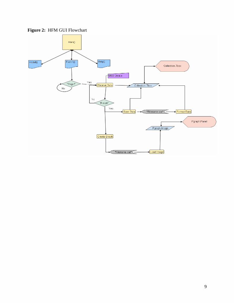
9
Figure 2: HFM GUI Flowchart

10
Budget
Table 1 represents the total budget of the original project. Nearly $215 was spent between
project supplies and hardware. The bulk of this expense came with the purchase of the necessary
directional and bidirectional couplers.
Item Cost Expenditures Cables, Solder, etc $ 72.92 $ 72.92 E-Days Supplies $ 17.06 $ 17.06 800MHz Bi-directional Coupler $ 17.34 $ 17.34 800MHz Bi-directional Coupler Evaluation Board $ 41.34 $ 41.34 Directional couplers (2 @ $33 ea.) $ 66.00 $ 66.00 Charting Software - Single Developer License $ 99.00 $ - AD8302 Evaluation Board $ 199.99 $ - Additional AD8302 Chips (2 @ $12 ea.) $ 24.00 $ - ADL5310 Evaluation Board $ 99.99 $ - PSoC Evaluation Board $ 96.95 $ - PSoC - ICE CUBE emulator $ 399.99 $ - PSoC Designer C-Compiler License $ 149.99 $ - Total Project Costs $ 1,284.57 $ 214.66 Current Total Available Budget SP’07 $ 400.00 Project Expenses to Date $ 214.66 Remaining Budget SP’07 $ 185.34 Projected Budget Carryover to FA’07 $ 100.00 Additional Budget for FA’07 $ 100.00 Total Available Budget FA’07 $ 200.00
This project never could have been completed under budget without the significant contributions
of Cypress Semiconductor, Analog Devices, and Advanced Software Engineering. These
companies donated software, evaluation boards, and other hardware totaling more than $1,000.
The project started with a budget of $300. With the addition of two new members during the
second half of the project, the budget increased to $400. The original $300 budget however, is
not transferable to the continuation of the project. As such, we have based our remaining budget

11
off of this nontransferable portion. We are now determining potential hardware and software
needs for project continuation in order that the remainder of the nontransferable budget might be
used to fund these expenses.
Chapter IV – Conclusions & Continuation
Conclusions:
The previous method of using torodial and capacitive pickups was thrown out in favor of the bi-
directional coupler for the proportional pick-off. Using this new method allowed a very
simplistic way of determining the reflection coefficient as that was the relative output of the
AD8302. This made the job of the PSoC simpler as fewer calculations were required thus
making the program more elegant. However, this does limit the ability to calculate power
characteristics due to the fact that we no longer have direct access to voltage and current values.
It is still possible to determine power when given input power and using the reflection coefficient
value. Finally, setting the PSoC USB interface with the host PC as a keyboard made input for
the host PC a relatively mundane task in comparison to writing a driver.
By the time of E-Days the device was functional for demonstration purposes and performed well.
The device was capable of communication with a host PC for real-time capture and display of
the reflection coefficient. The values of the reflection coefficient were verified against those
obtained using a Network Analyzer.

12
However, all of these accomplishments came at the cost of a slightly narrowed scope for the end
product. The project never created a PCB for miniaturization of the device due to time
constraints near the end of the semester however a preliminary design for one has been drawn up
and is prepared for next semester.
Possible Project Continuations:
Continuation of this project might consist of a change to wireless USB communication between
the Computer and PSoC. With frequencies in the gigahertz range being used in future revisions,
one can anticipate a challenge with the use of wireless communication in a reliable manner as
this is often difficult while accurately measuring RF signals.
Another element to the project which does not currently exist is automatic calibration. The
AD8302 is affected by the equipment which is connected to it. A useful option is the
implementation of a method to calibrate the system for a particular circuit. After making
connections in the circuit, there should be an option to account for this perturbation by redefining
the center point of the output.
In addition to this there are plans to create an automated impedance matching network. Using
the PSoC’s recorded values for the reflection coefficient, we can have a network that will go
through switching a variety of capacitors in series or shunt configurations and look for a
minimum value for the coefficient while looking for a minimum reflection coefficient. This
could be implemented in a variety of ways; the most feasible being a set of transistor/RF relay
combination, or pin-diode switched capacitors, using the PSoC to control the switching.

13
One last possible addition to the project would be to have the GUI supplying live updates in the
form of a graph, as well as implementing bi-directional communication between the PSoC and
host PC. Both of these will require writing libraries and maintaining active databases of
information, which will require a significant amount of time and resources which may or may
not be feasible in the time available in a single semester.

14
ACKNOWLEDGEMENTS Ken Dees of Cypress Semiconductor Corporation for meeting with the HFM team to explain the
intricacies of the PSoC board and its potential for our device. His clear presentation made the
PSoC environment not seem so overwhelming.
Peter Kwan of Advanced Software Engineering for the donation of the Graphing Library for the
GUI which improved our design. Without the donation of the software, libraries would have
taken up far too many resources and would not have been possible.
Dr. Cameron Moore for his vision of the project and willingness to meet with the HFM team on
an hours notice. His guidance has led the HFM team from fledgling to full blown senior design
project status. His provision of connections to people and industry expertise was indispensable.
His ability to acquire the evaluation boards for free largely made this project possible in the first
place based on budget constraints.
Glen Rothgery for the continuous stream of questions brought to him that were never left
unanswered. For the extra time he spent working with the HFM team in the ERC lab. His
expertise in locating needed parts and tools in the ERC cavernous expanse saved an exorbitant
amount of time for the HFM team.
Doug Scott for his constant help and discoveries with the AD8302. His help was critical to the
project; his help with the directional coupler and the AD8302 was priceless.

15
REFERENCES [1] PSoC TRM, Version 2.20. San Jose, CA: Cypress Semiconductor Corp.
[2] CY8C24794 Data Sheet. San Jose, CA: Cypress Semiconductor Corp.
[3] AD8302 Data Sheet. Norwood, MA: Analog Devices.
[4] ADL5310 Data Sheet. Norwood, MA: Analog Devices.

16
BIBLIOGRAPHY Impedance Matching. Fort Collins, CO: Advanced Energy Industries, Inc., 2006.
"Power Factor." Wikipedia. 3 Dec. 2006 <http://en.wikipedia.org/wiki/Power_factor>.
Scholl, Richard A. Forward and Reflected Powers. What Do They Mean? Fort Collins, CO:
Advanced Energy Industries, Inc., 1998.

I
APPENDIX
Figures and Tables
Figure 3: CY8C24794 PSoC Functional Block Diagram [2]

II
Figure 4: AD8302 Functional Block Diagram [3]
Figure 5: ADL5310 Functional Block Diagram [4]

III
Figure 6: CY8C24794 56-Pin PSoC Device [1]
Table 1: Pin Function Descriptions [1]
Type Pin
No. Digital Analog Name Description
1 IO I, M P2[3] Direct switched capacitor block input. 2 IO I, M P2[1] Direct switched capacitor block input. 3 IO M P4[7] 4 IO M P4[5] 5 IO M P4[3] 6 IO M P4[1] 7 IO M P3[7] 8 IO M P3[5] 9 IO M P3[3]

IV
10 IO M P3[1] 11 IO M P5[7] 12 IO M P5[5] 13 IO M P5[3] 14 IO M P5[1] 15 IO M P1[7] I2C Serial Clock (SCL) 16 IO M P1[5] I2C Serial Data (SDA) 17 IO M P1[3] 18 IO M P1[1] I2C Serial Clock(SCL), ISSP SCLK* 19 Power Vss Ground Connection 20 USB D+ 21 USB D- 22 Power Vdd Supply Voltage 23 IO P7[7] 24 IO P7[0] 25 IO M P1[0] ISC Serial Data (SDA), ISSP SDATA* 26 IO M 01[2] 27 IO M P1[4] 28 IO M P1[6] 29 IO M P5[0] 30 IO M P5[2] 31 IO M P5[4] 32 IO M P5[6] 33 IO M P3[0] 34 IO M P3[2] 35 IO M P3[4] 36 IO M P3[6] 37 IO M P4[0] 38 IO M P4[2] 39 IO M P4[4] 40 IO M P4[6] 41 IO I, M P2[0] Direct switched capacitor block input. 42 IO I, M P2[0] Direct switched capacitor block input. 43 IO M P2[2] External Analog Ground (AGND) input. 44 IO M P2[4] External Voltage Reference (VREF) input. 45 IO I, M P2[6] Analog column mux input. 46 IO I, M P0[0] Analog column mux input and column output. 47 IO I, M P0[2] Analog column mux input and column output. 48 IO I, M P0[4] Analog column mux input. 49 Power Vdd Supply voltage. 50 Power Vss Ground connection. 51 IO I, M P0[7] Analog column mux input, integration input #1.
52 IO IO, M
P0[5] Analog column mux input and column output, integration input #2.
53 IO IO, M P0[3] Analog column mux input and column output.

V
54 IO I, M P0[1] Analog column mux input. 55 IO M P2[7] 56 IO M P2[5]
Figure 7: AD8302 14-Pin Configuration [3]

VI
Table 2: Pin Function Descriptions
Pin No.
Mnemonic Function Equivalent Circuit
1, 7 COMM Device Common. Connect to low impedance ground 2 INPA High Input Impedance to Channel A. Must be ac-coupled Circuit A
3 OFSA A capacitor to ground at this pin sets the offset compensation filter corner and provides input decoupling
Circuit A
4 VPOS Voltage Supply (VS), 2.7 V to 5.5 V
5 OFSB A capacitor to ground at this pin sets the offset compensation filter corner and provides input decoupling.
Circuit A
6 INPB Input to Channel B. Same structure as INPA Circuit A 8 PFLT Low pass filter terminal for the phase output Circuit E
9 VPHS Single-ended output proportional to the phase difference between INPA and INPB
Circuit B
10 PSET Feedback pin for scaling of VPHS output voltage measurement mode. Accepts a set point voltage in controller mode.
Circuit D
11 VREF Internally generated reference voltage (1.8 V Nominal) Circuit C
12 MSET Feedback pin for scaling of VMAG output voltage measurement mode. Accepts a set point voltage in controller mode.
Circuit D
13 VMAG Single-ended output proportional to the decibel ratio of signals applied to INPA and INPB
Circuit B
14 MFLT Low pass filter terminal for the magnitude output Circuit E

VII
Figure 8: AD8302 Equivalent Circuits [3]
VIII
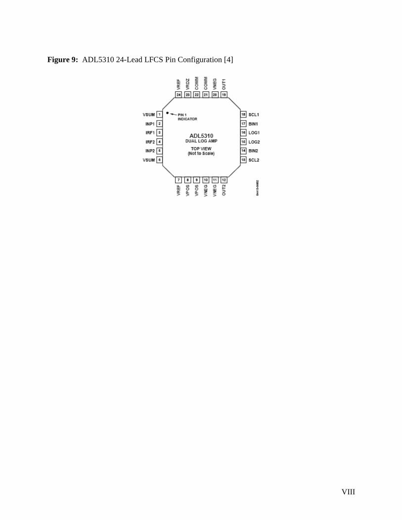
Figure 9: ADL5310 24-Lead LFCS Pin Configuration [4]

IX
Table 3: Pin Function Descriptions
Pin No.
Mnemonic Function
1, 6 VSUM Guard pin used to shield the INP1 and INP2 input current lines, and for optional adjustment of the input summing node potentials. Pin 1 and Pin 6 are internally shorted.
2 INP1 Channel 1 numerator input. Accepts (sinks) photodiode current IPD1. Usually connected to photodiode anode such that photocurrent flows into INP1.
3 IRF1 Channel 1 denominator input. Accepts (sinks) reference current, IRF1. 4 IRF2 Channel 2 denominator input. Accepts (sinks) reference current, IRF2. 5 INP2 Channel 2 numerator input. Accepts (sinks) photodiode current IPD2. Usually
connected to photodiode anode such that photocurrent flows into INP2. 7, 24 VREF Reference output voltage of 2.5 V. Pin 7 and Pin 24 are internally shorted. 8, 9 VPOS Positive supply, (VP – VN) ≤ 12 V. Both pins must be connected externally.
10, 11, 20
VNEG Optional negative supply, VN. These pins are usually grounded. All VNEG pins must be externally connected.
12 OUT2 Buffer output for channel 2. 13 SCL2 Buffer amplifier inverting input for channel 2. 14 BIN2 Buffer amplifier non-inverting input for channel 2. 15 LOG2 Output for the logarithmic front end for channel 2. 16 LOG1 Output for the logarithmic front end for channel 1. 17 BIN1 Buffer amplifier non-inverting input for channel 1. 18 SCL1 Buffer amplifier inverting input for channel 1. 19 OUT1 Buffer output for channel 1.
21, 22 COMM Analog ground. Pin 21 and Pin 22 are internally shorted. 23 VRDZ Intercept shift reference input. The top of a resistive divider network that
offsets VLOG to position the intercept. Normally connected to VREF; may also be connected to ground when bipolar outputs are to be provided.

X
Individual Project Roles
Stephanie Auyoung Project Task: (working with Joel) Get AD boards working and understand how the pick-off signals relate to chip output- i.e., calibrate them to get gain and offset of the output relative to inputs. This assumes a linear relationship. Prove or develop a higher-order (quadratic) relationship. After this constructing an enclosure for everything. Derek Hall Project Task: Assume a model for the signals that Joel and Stephanie will provide and determine how calibration will be performed in the PSoC. Also figure out if the calibration will be loaded in firmware once or whether there will be a way to re-calibrate on demand. After this we will determine the math operations that must be performed. Eric Hall Project Task: Webmaster. Responsible for creation of a GUI program that talks to the PSoC and gets the data and displays it, both instantaneous values as well as moving graph with history values. Joel Stanczyk Project Task: Working with Stephanie on the AD8302. Goal is to get the 8302 operational and to develop a suitable pickoff circuit for the device, effectively stepping down from a 1000 Watt supply to a half a volt or less input. End goal with the AD8302 is to receive inputs in RF and output a low voltage DC signal for the PSoC board to interpret for final analysis. Graphic Designer for website. Kevin Todd Project Task: Developing the PSoC end of the board for microcontroller interface between the AD8302 and the computer through USB data exchange. Programming for the PSoC.