High Fidelity Satellite Navigation Receiver Front-End for ...
155
Air Force Institute of Technology AFIT Scholar eses and Dissertations Student Graduate Works 3-22-2019 High Fidelity Satellite Navigation Receiver Front- End for Advanced Signal Quality Monitoring and Authentication Andrew D. Braun Follow this and additional works at: hps://scholar.afit.edu/etd Part of the Navigation, Guidance, Control and Dynamics Commons , and the Signal Processing Commons is esis is brought to you for free and open access by the Student Graduate Works at AFIT Scholar. It has been accepted for inclusion in eses and Dissertations by an authorized administrator of AFIT Scholar. For more information, please contact richard.mansfield@afit.edu. Recommended Citation Braun, Andrew D., "High Fidelity Satellite Navigation Receiver Front-End for Advanced Signal Quality Monitoring and Authentication" (2019). eses and Dissertations. 2248. hps://scholar.afit.edu/etd/2248
Transcript of High Fidelity Satellite Navigation Receiver Front-End for ...

Air Force Institute of TechnologyAFIT Scholar
Theses and Dissertations Student Graduate Works
3-22-2019
High Fidelity Satellite Navigation Receiver Front-End for Advanced Signal Quality Monitoring andAuthenticationAndrew D. Braun
Follow this and additional works at: https://scholar.afit.edu/etd
Part of the Navigation, Guidance, Control and Dynamics Commons, and the Signal ProcessingCommons
This Thesis is brought to you for free and open access by the Student Graduate Works at AFIT Scholar. It has been accepted for inclusion in Theses andDissertations by an authorized administrator of AFIT Scholar. For more information, please contact [email protected].
Recommended CitationBraun, Andrew D., "High Fidelity Satellite Navigation Receiver Front-End for Advanced Signal Quality Monitoring andAuthentication" (2019). Theses and Dissertations. 2248.https://scholar.afit.edu/etd/2248

HIGH FIDELITY SATELLITE NAVIGATION RECEIVER FRONT-END FOR
ADVANCED SIGNAL QUALITY MONITORING AND AUTHENTICATION
THESIS
Andrew D. Braun, USAF
AFIT-ENG-MS-19-M-013
DEPARTMENT OF THE AIR FORCE
AIR UNIVERSITY
AIR FORCE INSTITUTE OF TECHNOLOGY
Wright-Patterson Air Force Base, Ohio
DISTRIBUTION STATEMENT A.
APPROVED FOR PUBLIC RELEASE; DISTRIBUTION UNLIMITED.

The views expressed in this thesis are those of the author and do not reflect the official
policy or position of the United States Air Force, Department of Defense, or the United
States Government. This material is declared a work of the U.S. Government and is not
subject to copyright protection in the United States.

AFIT-ENG-MS-19-M-013
HIGH FIDELITY SATELLITE NAVIGATION RECEIVER FRONT-END FOR
ADVANCED SIGNAL QUALITY MONITORING AND AUTHENTICATION
THESIS
Presented to the Faculty
Department of Electrical and Computer Engineering
Graduate School of Engineering and Management
Air Force Institute of Technology
Air University
Air Education and Training Command
In Partial Fulfillment of the Requirements for the
Degree of Master of Electrical Engineering
Andrew D. Braun, BS
USAF
March 2019
DISTRIBUTION STATEMENT A.
APPROVED FOR PUBLIC RELEASE; DISTRIBUTION UNLIMITED.

AFIT-ENG-MS-19-M-013
HIGH FIDELITY SATELLITE NAVIGATION RECEIVER FRONT-END FOR
ADVANCED SIGNAL QUALITY MONITORING AND AUTHENTICATION
Andrew D. Braun, BS
USAF
Committee Membership:
Dr. Sanjeev Gunawardena
Chair
Dr. Richard Martin
Member
Dr. Jeff Hebert
Member
iv
AFIT-ENG-MS-19-M-013
Abstract
Over the past several years, interest in utilizing foreign satellite timing and
navigation (satnav) signals to augment GPS has grown. Doing so is not without risks;
foreign satnav signals must be vetted and determined to be trustworthy before use in
military applications. Advanced signal quality monitoring methods can help to ensure
that only authentic and reliable satnav signals are utilized. To effectively monitor and
authenticate signals, the receiver’s front-end must impress as little distortions upon the
signal as possible. The purpose of this study is to design, fabricate, and test the
performance of a high-fidelity satnav receiver front-end for advanced monitoring of
foreign and domestic space vehicle (SV) signals.
Advanced satnav integrity checking and authentication extends beyond range
measurement based techniques such as receiver autonomous integrity monitoring
(RAIM) and fault detection and exclusion (FDE). Monitoring signal deformations and
spreading code chip asymmetries that are characteristic to specific space vehicles can
significantly extend satnav signal quality monitoring and authentication capabilities [1].
In order to procure high fidelity nominal satnav signal deformations that may serve as a
reference, the front-end of the receiver must not impress any deformations of its own. A
database of nominal signal features can then be used to ascertain what is authentic versus
inauthentic operation.
Current commercial receiver technology does not perform high fidelity
correlation monitoring or distinguish spreading code chip asymmetries between different
v
SVs. These techniques benefit from a high fidelity front-end that cannot be purchased off
the shelf. Chip-shape out of the satnav signal processing requires extended coherent
integration times and narrow tracking loop bandwidths [1]. The stability of the reference
oscillator and phase noise contributed by the frequency synthesizer limits the
effectiveness of long coherent integration [2]. Thus, a highly stable reference oscillator
and low phase noise frequency synthesizer are used in this front-end. Group delay
variations of filters in a receiver front-end adds distortions to the satnav signals and can
create pseudorange biases [3],[4]. To preserve the received signal’s nominal signal
characteristics, group delay variations of filters are minimized over the front-end’s
passband.
The front-end utilizes a superheterodyne architecture to convert satnav signals
down to an intermediate frequency, in which it is bandpass sampled by a high bandwidth,
high dynamic range analog-to-digital converter (ADC). Unlike the commonly used direct
downconversion receiver that is plagued by inphase/quadrature (I/Q) gain and phase
imbalances that can significantly impact received signal observables, this architecture
produces a real stream of digitized samples that guarantees zero I/Q imbalance since
quadrature downconversion is performed digitally. The front-end is designed to the
OpenVPX 3U card form factor and consumes less than 3.5 Watts of power. Digital
attenuators and root-mean-squared (RMS) power detectors are utilized to enable
software-defined smart gain control to preserve linearity, maintain a low noise figure, and
rapidly respond to interference. The front-end developed in this thesis is uniquely suited
for use in high fidelity all-domain satnav signal monitoring. These domains include time
domain, frequency domain, correlation domain (i.e. chip shape), spatial domain (using
vi
multi-element controlled reception pattern antennas (CRPAs)), and polarization domain
(using dual-polarized antenna elements in a CRPA). The results presented offer
significant advancements towards high-fidelity satnav constellation monitoring and
characterization, and next-generation navigation warfare (NAVWAR) applications.

vii
Acknowledgments
I would like to give thanks to God for the opportunities to struggle and grow in
perseverance.
A big thank you to my parents. Being electrical engineers themselves, they have
always fortified education and scientific exploration. The success of this thesis would not
have been possible if not for their endless support and encouragement throughout my
academic career. Thank you to my siblings who have always been a source of
encouragement and inspiration.
I would like to offer my sincere gratitude and appreciation to my advisor Dr.
Sanjeev Gunawardena. Having started the thesis with virtually no electronics or RF
experience, under his guidance I was able to achieve something I did not think I could
accomplish. He has been a great source of motivation and inspiration through the
duration of the thesis. By his own example and patience, he has helped instill a desire to
work hard and persevere.
I would like to thank my committee members, Dr. Martin and Dr. Hebert for their
valuable time and technical input toward this thesis.
None of this work would have been possible if not for the sponsorship of
AFRL/RYWN; for that I am sincerely grateful. To have the opportunity to design, build,
and test state-of-art technology with world class instruments and tools has been an
extremely rewarding experience.
Thank you to Pranav and Jorge for assisting me in operating the RF
instrumentation and PCB assembly equipment. They have never hesitated to lend a hand.
A special thank you to my colleagues from LCMC. They had involved and
tutored me in several high impact projects as an inexperienced engineer. By doing so,
they had inspired me to pursue GPS related topics at AFIT.
Andrew D. Braun
viii
Table of Contents
Page
Abstract .............................................................................................................................. iv
Acknowledgments............................................................................................................. vii
List of Figures .................................................................................................................... xi
List of Tables ................................................................................................................... xvi
List of Acronyms ............................................................................................................ xvii
I. Introduction ..................................................................................................................1
1.1 General Issue/Motivation ....................................................................................1
1.2 Problem Statement ..............................................................................................2
II. Background/Literature Review ....................................................................................4
2.1 Chapter Overview ...............................................................................................4
2.2 Satnav Signal Overview ......................................................................................4
2.3 Gain, Noise Figure and Sensitivity .....................................................................6
2.4 Linearity ..............................................................................................................7
2.5 Dynamic Range ...................................................................................................9
2.6 Mixer .................................................................................................................10
2.7 Image Rejection.................................................................................................11
2.8 Selectivity ..........................................................................................................12
2.9 Receiver Architectures ......................................................................................12
2.10 Reference Oscillator.......................................................................................18
2.11 Frequency Synthesizer Phase Locked Loop ..................................................23
2.12 Group Delay Variations .................................................................................28
2.13 RF Filters for Satnav Instrumentation............................................................29
2.14 IF / Antialiasing Filters ..................................................................................30

ix
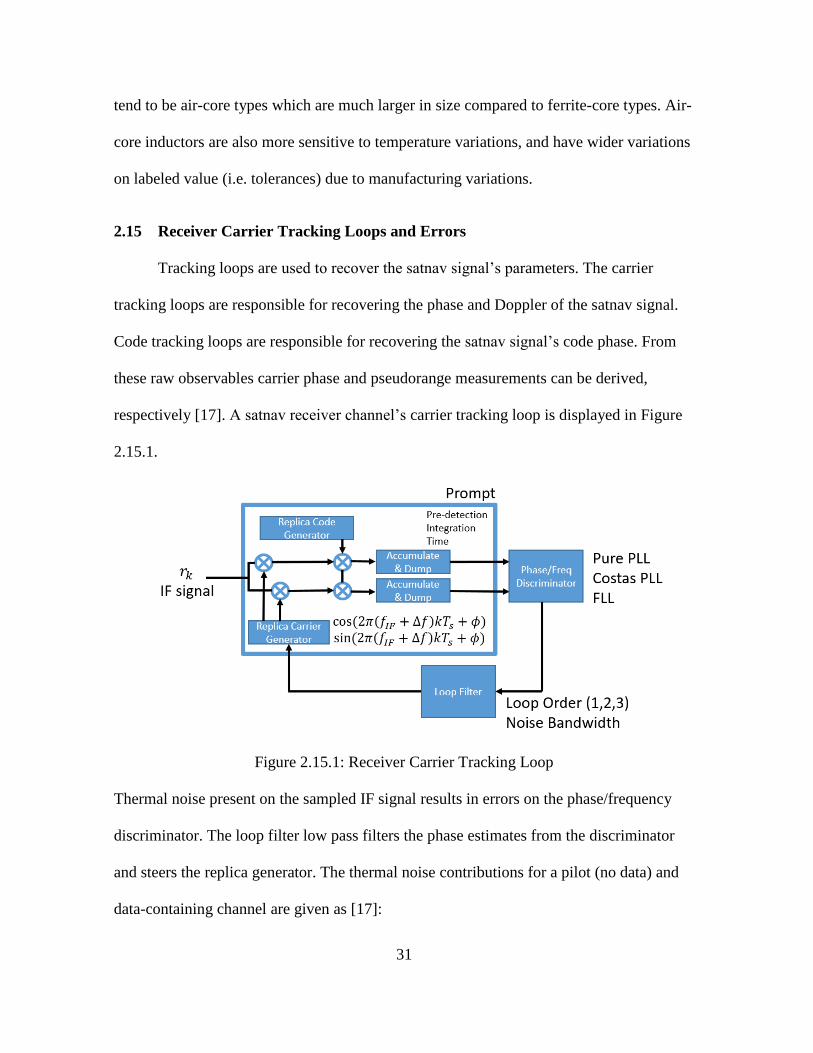
2.15 Receiver Carrier Tracking Loops and Errors .................................................31
III. Methodology ..............................................................................................................35
3.1 Chapter Overview .............................................................................................35
3.2 Receiver Architectures ......................................................................................36
3.3 Analog to Digital Converter ..............................................................................36
3.4 Bandpass Antialiasing Filter .............................................................................40
3.5 RF Image Rejection Filter .................................................................................44
3.6 Reference Oscillator ..........................................................................................51
3.7 Frequency Synthesizer Phase Locked Loop......................................................52
3.8 Gain Control and Linearity for the ADC ..........................................................56
3.9 RMS Power Detector ........................................................................................60
3.10 Gain Control, Noise Figure and Linearity RF Calculator ..............................61
3.11 Nonlinear Simulation of Front-End ...............................................................68
IV. Analysis and Results ..................................................................................................71
4.1 Introduction .......................................................................................................71
4.2 Waveguide Evaluation ......................................................................................72
4.3 Front-End Low Noise Amplifier Evaluation .....................................................74
4.4 Frequency Synthesizer Evaluation ....................................................................76
4.5 Frequency Synthesizer Design ..........................................................................89
4.6 Power Supply Design ........................................................................................92
4.7 IF Filter Design .................................................................................................94
4.8 RF Portion of RF Front-End Design .................................................................96
4.9 IF Portion of RF Front-End Design.................................................................101
x
4.10 Analog to Digital Converter Evaluation Results .........................................104
4.11 Software Defined Satnav Signal Tracking & Front-End Results ................107
V. Conclusions and Recommendations .........................................................................122
5.1 Conclusions of Research .................................................................................122
5.2 Significance of Research .................................................................................123
5.3 Recommendations for Future Research ..........................................................124
5.4 Summary .........................................................................................................125
Appendix A: PCB Stack Up ............................................................................................126
Appendix B: 3D Render...................................................................................................127
Bibliography ....................................................................................................................128

xi
List of Figures
Page
Figure 2.4.1: 3rd Order Intermodulation Products ............................................................... 8
Figure 2.6.1: Mixer Signal Translation ............................................................................. 10
Figure 2.7.1: Image Frequency with Respect to LO ......................................................... 11
Figure 2.9.1: Direct Conversion Receiver Architecture ................................................... 13
Figure 2.9.2: LO to RF Isolation at the Mixer .................................................................. 14
Figure 2.9.3: Direct RF Sampling Receiver Architecture................................................. 16
Figure 2.9.4: Superheterodyne Receiver Architecture ...................................................... 17
Figure 2.10.1: Two State Clock Process Noise Model [8] ............................................... 19
Figure 2.10.2: SSB Calculated Phase Noise of OCXO1 ................................................... 21
Figure 2.10.3: Allan Variance Calculation ....................................................................... 22
Figure 2.10.4: Simulated vs. Calculated Allan Variance .................................................. 23
Figure 2.11.1: Integer-N PLL with 2nd-Order Loop Filter ................................................ 24
Figure 2.11.2: LTI Phase Domain Model with Additive Noise Sources .......................... 25
Figure 2.11.3: FSPLL Simulated Phase Noise and Measured Phase Noise from LMX
2582 In its 1st Configuration ...................................................................................... 27
Figure 2.15.1: Receiver Carrier Tracking Loop ................................................................ 31
Figure 3.3.1: Nyquist Zones of the Analog Devices AD 9681 ADC ............................... 37
Figure 3.3.2: 1st Nyquist Zone Frequency Overlap........................................................... 38
Figure 3.3.3: 3rd Nyquist Zone Frequency Response ........................................................ 39
Figure 3.3.4: Frequency Plan of the Receiver Front-End ................................................. 39
Figure 3.4.1: Genesys IF Filter Using Theoretical Components ...................................... 42

xii
Figure 3.4.2: Frequency Response of Vendor Part Syntheis and Theoretical of IF Filter 43
Figure 3.4.3: Group Delay Response of Vendor Part Syntheis and Theoretical Deisng of
IF Filter ....................................................................................................................... 44
Figure 3.5.1: Group Delay, Image Rejection, and Frequency Response of RF Filter
Configurations ............................................................................................................ 46
Figure 3.5.2: Five Resonator Ceramic RF Filter Image Rejection ................................... 47
Figure 3.5.3: Four Resonator Ceramic RF Filter Image Rejection ................................... 48
Figure 3.5.4: Four Resonator Ceramic RF Filter Image Rejection ................................... 49
Figure 3.5.5: Group Delay of RF Bandpass Filters .......................................................... 50
Figure 3.6.1: 10 MHz OCXO Reference Oscillator SSB Phase Noise ............................. 52
Figure 3.8.1: ADC Operation at -97 dBm Input Power .................................................... 57
Figure 3.8.2: ADC Operation at -43 dBm Input Power .................................................... 58
Figure 3.8.3: ADC Operation at Full Scale Input Power (-27 dBm) ................................ 59
Figure 3.9.1: RMS Power Detector Signal Path ............................................................... 60
Figure 3.11.1: Genesys Nonlinear Signal Path Simulation .............................................. 68
Figure 3.11.2: Gain and Linearity at -97 dBm Operation ................................................. 69
Figure 3.11.3: Gain and Linearity at -26 dBm Operation ................................................. 70
Figure 4.2.1: CPWG Evaluation Board ............................................................................ 72
Figure 4.2.2: CPWG S11 for Difference Dimensions ...................................................... 73
Figure 4.2.3: CPWG Isolation .......................................................................................... 73
Figure 4.3.1: Left: MACOM Evaluation Board, Right: Constructed Evaluation Board .. 74
Figure 4.3.2: MAL-010704 LNA Gain and Linearity vs. Bias ......................................... 75
Figure 4.3.3: S11 of MAL-010704 LNA .......................................................................... 76
xiii
Figure 4.4.1: Charge Pump, Loop Filter components and VCO Circuit .......................... 77
Figure 4.4.2: LMX 2582 Evaluation Board from Texas Instruments ............................... 78
Figure 4.4.3: ADF 4355-2 Evaluation Board from Analog Devices ................................ 79
Figure 4.4.4: MAX 2871 Evaluation Board from Maxim Integrated ............................... 80
Figure 4.4.5: HMC 830 Evaluation Board from Hittite (Analog Devices) ...................... 81
Figure 4.4.6: LMX 2582 Spurs in Configuration # 1 ....................................................... 83
Figure 4.4.7: HMC 830 Spurs in Configuration # 1 ......................................................... 84
Figure 4.4.8: Phase Noise Collection with the Keysight PXA 9030B Spectrum Analyzer
[39] ............................................................................................................................. 86
Figure 4.4.9: Phase Noise Measurements Taken from the Best Performing Configurations
on Each Device .......................................................................................................... 88
Figure 4.5.1: Constructed LMX 2582 Circuit ................................................................... 90
Figure 4.5.2: LMX 2582 Phase Noise at L1, L2, L5 LO .................................................. 91
Figure 4.6.1: Front-End Power Supply Linear Voltage Regulators.................................. 92
Figure 4.6.2: 5.0 V Linear Regulator Power from ADP3339 [40] ................................... 93
Figure 4.6.3: 3.3 V Linear Power Regulator from ADM7150 [41] .................................. 93
Figure 4.6.4: 6.0 V Power Supplied Through BK Precision [35] ..................................... 94
Figure 4.7.1: IF Filter Assembled on a Surface Mount PCB ............................................ 94
Figure 4.7.2: IF Filter Response and Repeatability .......................................................... 95
Figure 4.7.3: IF Filter Group Delay and Repeatability ..................................................... 96
Figure 4.8.1: RF Portion and Layout of the Front-End..................................................... 97
Figure 4.8.2: First RF Room Gain and Linearity .............................................................. 98
Figure 4.8.3: RF Gain and Linearity of RF Signal-Path ................................................... 99
xiv
Figure 4.8.4: Group Delay of RF Signal Path ................................................................. 100
Figure 4.8.5: RF Filter Response of Signal Path ............................................................ 101
Figure 4.9.1: IF Portion of the Front-End ....................................................................... 102
Figure 4.9.2: IF Portion Gain and Linearity of the Front-End ........................................ 103
Figure 4.9.3: IF Portion Response and Group Delay of the Front-End .......................... 104
Figure 4.10.1: AD 9681 Evaluation Board ..................................................................... 105
Figure 4.10.2: ADC PSD from Live-sky Antenna .......................................................... 106
Figure 4.11.1: RF Front-End Under Test ........................................................................ 107
Figure 4.11.2: RF Front-End Under Test with Arduino and ADC ................................. 108
Figure 4.11.3: Simulated Satnav Signal Testbed with LMX 2582 LO ........................... 109
Figure 4.11.4: PSD and Time-Domain Sample Snapshot of R&S Simulated Satnav Data
.................................................................................................................................. 110
Figure 4.11.5: Measured CNR When Using the LMX 2582 as the LO.......................... 111
Figure 4.11.6: Carrier Filter Tracking States LMX 2582 PLL LO ................................. 112
Figure 4.11.7: Simulated Satnav Signal Testbed with Synergy Microwave LO ............ 113
Figure 4.11.8: CNR Measurements Using the LMX 2582 LO and the Synergy Microwave
LO ............................................................................................................................ 113
Figure 4.11.9: Carrier Filter Tracking States Using the Synergy Microwave FSPLL as LO
Plotted Overtop the TI LMX 2582 ........................................................................... 115
Figure 4.11.10: CNR Measured from Septentrio PolaRx5 Receiver .............................. 116
Figure 4.11.11: Carrier Phase Measurement Residues with Septentrio PolaRx5 ........... 117
Figure 4.11.12: Live-sky Satnav Signal with LMX 2582 LO ........................................ 118
Figure 4.11.13: L1-Band Live-sky Capture 62.5 MHz of Bandwidth PSD ................... 118

xv
Figure 4.11.14: PRN 08 C/A Acquisition of Live-sky Signals ....................................... 119
Figure 4.11.15: Live-Sky PRN 08 C/A Carrier Tracking Loop Output ......................... 120
Figure 4.11.16: Live-Sky CNR of Tracked PRN 08 ....................................................... 120
Figure 4.11.17: Live-Sky Carrier Tracking Lock Indicator for PRN 08 ........................ 121
xvi
List of Tables
Page
Table 2.10.1: Allan Variance Power Coefficients for Typical Oscillators ....................... 21
Table 2.15.1: Typical Loop Filter Values ......................................................................... 33
Table 3.10.1: Gain, Linearity and Noise Figure of Front-End with Passive Antenna -
97dBm ........................................................................................................................ 62
Table 3.10.2: Gain, Linearity and Noise Figure of Front-End -46 dBm Input ................. 65
Table 3.10.3: Linearity, Gain and Noise Figure of Front-End at Full Scale -26dBm ...... 67
Table 4.3.1: MAL-010704 LNA Current Consumption ................................................... 76
Table 4.4.1: LMX 2582 Configurations ........................................................................... 78
Table 4.4.2: ADF 4355-2 Configurations ......................................................................... 79
Table 4.4.3: MAX 2871 Configurations ........................................................................... 80
Table 4.4.4: HMC 830 Configurations ............................................................................. 81
Table 4.4.5: LMX 2582 Spur Powers (dBc) ..................................................................... 82
Table 4.4.6: ADF 4355-2 Spur Powers (dBc)................................................................... 83
Table 4.4.7: MAX 2871 Spur Powers (dBc)..................................................................... 84
Table 4.4.8: HMC 830 Spur Powers (dBc) ....................................................................... 84
Table 4.4.9: LMX 2582 Integrated Phase Noise RMS Error ............................................ 86
Table 4.4.10: ADF 4355-2 Integrated Phase Noise RMS Error ....................................... 87
Table 4.4.11: MAX 2871 Integrated Phase Noise RMS Error ......................................... 87
Table 4.4.12: HMC 830 Integrated Phase Noise RMS Error ........................................... 87
Table 4.5.1: Frequency Synthesizer Performance vs Reference Oscillator ...................... 91
xvii
List of Acronyms
ADC Analog to Digital Converter
AGC Automatic Gain Control
BPF Bandpass Filter
BPSK Binary Phase Shift Keying
CDMA Code Division Multiple Access
CNR Carrier to Noise Ratio
CPWG Coplanar Waveguide
DC Direct Current
ENOB Effective Number of Bits
EMI Electromagnetic Interference
FDMA Frequency Division Multiple Access
FSPLL Frequency Synthesizer Phase Locked Loop
FFM Flicker Frequency Modulation
GPS Global Positioning System
GLONASS Globalnaya Navigazionnaya Sputnikovaya Sistema
IEEE Institute of Electronics and Electrical Engineers
IF Intermediate Frequency
IQ In-phase and Quadrature Phase
IRNSS Indian Regional Navigation Satellite System
LPF Low Pass Filter
LNA Low Noise Amplifier
LO Local Oscillator
xviii
MMIC Monolithic Microwave Integrated Circuit
OCXO Oven Controlled Crystal Oscillator
OIP3 Output 3rd Order Intercept Point
OIP1 Output 1dB Saturation Point
OPSAT Output Saturation Point
PCB Printed Circuit Board
PFD Phase Frequency Detector
PLL Phase Locked Loop
PNT Position Navigation and Timing
PRN Pseudorandom Number
PSD Power Spectral Density
RF Radio Frequency
RMS Root Mean Square
RWFM Random Walk Frequency Modulation
RO Reference Oscillator
QZSS Quasi-Zenith Satellite System
SDR Software Defined Radio
SNR Signal to Noise Ratio
SRF Self Resonate Frequency
SV Space Vehicle
TCXO Temperature Compensated Crystal Oscillator
VCO Voltage Controlled Oscillator
VNA Vector Network Analyzer

xix
WFM White Frequency Modulation
WSS Wide Sense Stationary
XO Crystal Oscillator
1
HIGH FIDELITY SATELLITE NAVIGATION FRONT-END FOR SIGNAL
QUALITY MONITORING AND ADVANCED AUTHENTICATION
I. Introduction
1.1 General Issue/Motivation
For military and civilian applications, having reliable and trustworthy satnav
signals is of paramount importance. Many civilian applications depend on the integrity of
satnav signals; a few major applications include precision aircraft landing and approach,
finance and banking transactions, cargo shipping lanes, power grid synchronization,
cellular networks, autonomous navigation, railway operations, survey, and precision
agriculture. As the dependence upon satnav signals grow, so do the implications of signal
disruptions. Interference can quickly overcome receivers, denying position-navigation-
timing (PNT) capability. Software defined radios (SDRs) can pose a new threat in the
hands of a nefarious actor. The implications of a receiver computing a false PNT solution
can be seriously detrimental in many applications.
Advanced signal and spectrum monitoring and using foreign satnav signals can
mitigate the threats posed toward military and civilian receivers. The monitoring
equipment can provide civilian and military receivers with situational awareness
preventing false and inaccurate PNT solutions.
High fidelity satnav signal monitoring entails providing nominal measurements of
the deformations impressed upon the signal by the satellites themselves. These natural
signal deformations are caused by the filter responses, amplifiers, and frequency
synthesizer in the satellite. These deformations result in a unique "chip shape" in the

2
broadcast pseudo-random number (PRN) codes. Some of these deformations are distinct
to specific satellites [1]. By measuring the nominal signal characteristics of the satnav
signals, receivers can begin to distinguish authentic satnav signals from those that may be
transmitted by bad actors.
High fidelity monitoring in spectrally diverse locations where strong interference
may be present is an important capability to have. The advanced monitoring receiver
would be able to detect and quantize interference with enough dynamic range to perform
later analysis on it.
Unique design challenges arise in engineering a high-fidelity satnav signal monitor.
Traditional commercial-off-the-shelf (COTS) satnav receivers are inadequate. Users have
little to no control of the correlators and tracking loops within the receiver due to
proprietary architectures. Users have no access to the digital samples, and the RF front-
end lacks in performance. The RF front-end of the receiver is perhaps the most important
component for high fidelity satnav monitoring. The purpose of this thesis is that very
topic. In order to preserve the natural signal deformations characteristic of specific
satellites, the front-end must impress as little deformations as possible on the received
signals. This entails careful selection and design of the filters, reference oscillator (RO),
frequency synthesizer, amplifies, and sample rate.
1.2 Problem Statement
The purpose of this study is to design, fabricate, and test the performance of high-
fidelity satnav receiver RF front-ends that are capable of instrumentation-grade signal
analysis. An instrumentation-grade satnav front-end provides the analog-to-digital-

3
converter (ADC) with minimum distortions and noise not already present on the signal.
Measurements computed with known satnav algorithms can then be used as a baseline
against other receivers [1]. The frequency synthesizer phase-locked loop (FSPLL), group
delay of filters, and linearity of the front-end are the major research thrusts in this study.
4
II. Background/Literature Review
2.1 Chapter Overview
This chapter discusses the basics of satnav signals, receiver front-ends and signal
tracking. An overview of the satnav signal structure is provided for multiple
constellations. Receiver operating characteristics are discussed including signal-to-noise
ratio (SNR), carrier-to-noise ratio (CNR), gain, noise figure, linearity, group delay,
frequency plan, reference oscillator and frequency synthesizers. Detrimental effects to the
receiver’s signal tracking ability are also described.
2.2 Satnav Signal Overview
The satnav signals of interest for this study reside in the Institute of Electrical and
Electronic Engineers (IEEE) L-Band spanning from 1-2 GHz [5]. The L-Band is a very
spectrally dense and highly sought-after portion of the electromagnetic spectrum due to its
desirable atmospheric propagation properties. In particular for space-to-ground and
ground-to-space communications and navigation.
The Global Positioning System (GPS) is a USAF owned and operated satnav
system and consists of a satellite constellation in medium earth orbit (MEO). Other
countries and alliances have procured their own satellite navigation constellations. Japan
and India operate regional satnav capabilities QZSS and NAVIC respectively. The
European Space Agency (ESA) has fielded Galileo. The Russian Federation has fielded
GLONASS. The People’s Republic of China has fielded BeiDou.

5
Satnav signals are broadcasted on several frequencies in the L-Band. The GPS
Link-1 (L1) band is centered at 1575.42 MHz and is the major focus of this study. Satnav
signals are also broadcast on L2 (1227.60 MHz) and L5 (1176.45 MHz) for GPS and
several other constellations. GPS, BeiDou, (modernized) GLONASS, and Galileo are
global systems that have satnav signals on the L1 band.
Besides the legacy GLONASS signals, all satnav signals use code-division-
multiple-access (CDMA). Psuedo-random number (PRN) codes that are orthogonal from
one another are used to distinguish satellites and offer ranging precision to the receiver.
The PRN codes are phase modulated along with data containing orbital parameters
(known as ephemeris), timing, and satellite health information.
2.2.1 SNR and CNR
SNR is a dimensionless measurement and usually expressed in terms of dB as:
𝑆𝑁𝑅 (𝑑𝐵) = 10 log10
𝑆𝑖𝑔𝑛𝑎𝑙 𝑃𝑜𝑤𝑒𝑟 (𝑊)
𝑁𝑜𝑖𝑠𝑒 𝑃𝑜𝑤𝑒𝑟 (𝑊)= 𝑆𝑖𝑔𝑛𝑎𝑙 (𝑑𝐵𝑊) − 𝑁𝑜𝑖𝑠𝑒 (𝑑𝐵𝑊). (1)
All front-end components contribute to the noise figure, starting with the thermal noise of
the antenna. Thermal noise is modeled as a stationary white random process, with a
variance of 𝜎𝑛02 . The thermal noise power for a given temperature and bandwidth is given
as:

6
𝑛0(𝑡)~𝑁(0, 𝜎𝑛02 ), (2)
𝜎𝑛02 = 𝑘𝐵𝑇0𝐵𝑓𝑒, (3)
where 𝑘𝐵 is Boltzmann’s constant 1.38E-23 Joules / Kelvin, 𝑇0 is the effective noise
temperature in Kelvin, and 𝐵𝑓𝑒 is the bandwidth of the receiver’s front-end. For a receiver
at room temperature, 𝑇0 = 290𝐾, and 𝐵𝑓𝑒 = 50𝑀𝐻𝑧; the thermal noise power is -127
dBW. The thermal noise within a 1 Hz bandwidth is -204 dBW/Hz. For an isotropic
antenna, the minimum received signal power for the L1 C/A signal is -159 dBW, and -157
dBW for the new L1C signal. Thus the SNR for the L1 C/A signal is – 159 dBW – ( –
127 dBW) = – 32 dB. The received satnav signal is – 32 dB below the thermal noise
power for a 50 MHz bandwidth front-end. Equivalently, the thermal noise power is 1585
times stronger than the received satnav signal. Carrier-to-Noise-Density Ratio (CNR) is
bandwidth agnostic because it considers the noise in a 1 Hz bandwidth and is given as:
𝐶
𝑁0= 𝑆𝑁𝑅 (𝑑𝐵) + 10 log10 𝐵𝑓𝑒 = −32 (𝑑𝐵) + 77 (Hz) = 45 (dB − Hz). (4)
2.3 Gain, Noise Figure and Sensitivity
The noise factor of a system is the amount of SNR degradation that a signal
experiences as it passes through the system. Noise factor expressed in dB is referred to as
noise figure.
A receiver front-end is a cascade of many analog RF components, the antenna,
filter, amplifier, transmission line, and mixers. All of which contribute a gain or loss, and
a noise factor (NF). The noise factor and gain for a series of components in a signal path
can be calculated using Friis Formula [5]:

7
𝐹 = 𝐹1 +𝐹2 − 1
𝐺1+
𝐹3 − 1
𝐺1𝐺2+
𝐹4 − 1
𝐺1𝐺2𝐺3+
𝐹𝑛 − 1
𝐺1𝐺2𝐺3 … 𝐺𝑛−1, (5)
𝐺 = 𝐺1𝐺23… 𝐺𝑛, (6)
where 𝐺𝑛 are the gains of each device and 𝐹𝑛 is the noise factor. It is apparent that the first
several components in the signal path are the most significant for setting the noise figure
of the front-end. Lossy components such as filters and transmission lines can degrade the
noise figure and SNR if the satnav signal has not been adequately amplified. Sensitivity is
determined by the noise figure of the receiver. It is the lowest possible received signal
power at the antenna that the downstream signal processing can detect [6].
2.4 Linearity
Active devices such as amplifiers and analog-to-digital converters (ADCs) need to
operate in their linear region in order to preserve the natural satnav signal characteristics.
If an excessive amount of input power is supplied to an active device, it will saturate
(experience non-linear behavior) and create harmonics and intermodulation products on
the output.
Device manufactures supply operating points for their components to users in the
form of datasheets. It is the responsibility of the designer to keep all the devices in the
signal path operating in the linear region throughout the expected signal dynamic range.
Manufactures typically supply the gain, noise figure, output power 3rd order intercept
point, and output power 1 dB saturation point.
The 3rd order intercept point describes the nonlinearity of a system. 3rd order
modulation products lie much closer to the input signals and are therefore more likely to
8
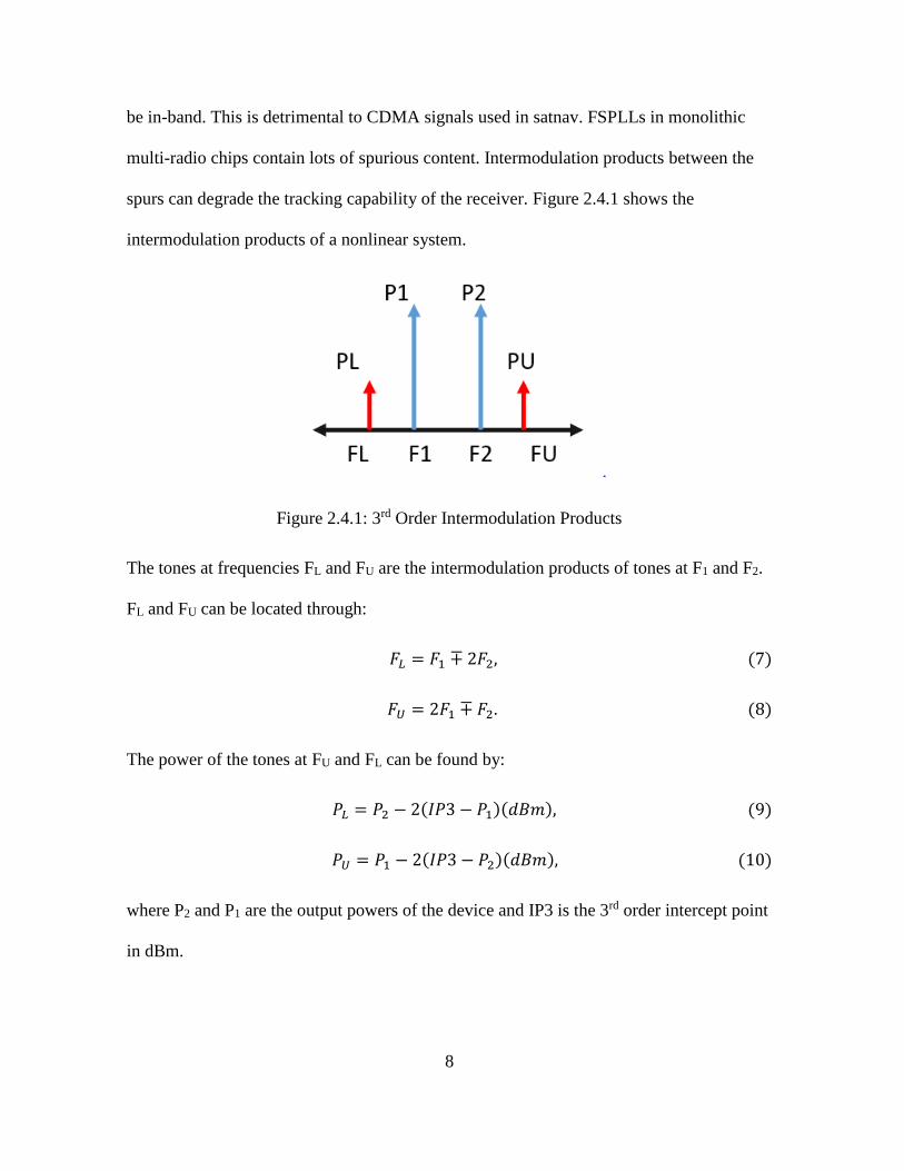
be in-band. This is detrimental to CDMA signals used in satnav. FSPLLs in monolithic
multi-radio chips contain lots of spurious content. Intermodulation products between the
spurs can degrade the tracking capability of the receiver. Figure 2.4.1 shows the
intermodulation products of a nonlinear system.
Figure 2.4.1: 3rd Order Intermodulation Products
The tones at frequencies FL and FU are the intermodulation products of tones at F1 and F2.
FL and FU can be located through:
𝐹𝐿 = 𝐹1 ∓ 2𝐹2, (7)
𝐹𝑈 = 2𝐹1 ∓ 𝐹2. (8)
The power of the tones at FU and FL can be found by:
𝑃𝐿 = 𝑃2 − 2(𝐼𝑃3 − 𝑃1)(𝑑𝐵𝑚), (9)
𝑃𝑈 = 𝑃1 − 2(𝐼𝑃3 − 𝑃2)(𝑑𝐵𝑚), (10)
where P2 and P1 are the output powers of the device and IP3 is the 3rd order intercept point
in dBm.

9
A receiver front-end is a cascade of many active and passive components.
Therefore, it useful to know cascaded 3rd order intercept point for a receiver. The 3rd order
intercept for a cascade of signal components is given as:
𝑖𝑝3𝑐 =1
1𝑖𝑝3𝑁−1 ∗ 𝑔𝑁
+1
𝑖𝑝3𝑁
(𝑚𝑊). (11)
All terms are expressed in mW. 𝑔𝑁 is the gain of the Nth device. 𝑖𝑝3𝑐 is the 3rd order
intercept point up to the Nth device expressed in mW.
2nd order intermodulation products occur at F1 ± F2. This is generally not a
significant problem for superheterodyne receivers since the intermodulation products
occur out-of-band. However, for direct conversion receivers, the intermodulation products
are produced within the passband of the baseband signal and can severely degrade SNR
(receiver architectures are covered in Section 2.9).
The 1 dB saturation point is the device’s output power that diverges from the linear
relationship between input/output power by 1 dB. It is up to the designer to not approach
that point to ensure linear operation of the front-end.
2.5 Dynamic Range
Dynamic range is the difference between the smallest detectable signal power and
the largest received signal power that the front-end can handle without saturating. A
satnav front-end for signal monitoring and instrumentation purposes requires a high
dynamic range due to the possibility of a diverse operating environment. Large amounts of
interference may be present in the satnav signal band, which has the possibility of
saturating the front-end if preventive measures are not taken. Further, for instrumentation
10
applications, the desire is to receive strong interference with no front-end saturation such
that the interference can be carefully analyzed. This is significantly different to other
satnav receiver front-ends where the goal is to merely reject the interference as much as
possible.
The ADC also plays an important role in the dynamic range. The effective number
of bits (ENOB) is the amount of bits that have not been degraded by noise. The input
range is usually specified in volts from the manufacture. Each bit of the ADC represents 6
dB of dynamic range. It is the front-end’s responsibility to adjust the gain of the input
signal to excite the appropriate bits of the ADC. More is discussed in Section 3.8 Gain
Control and Linearity for the ADC.
2.6 Mixer
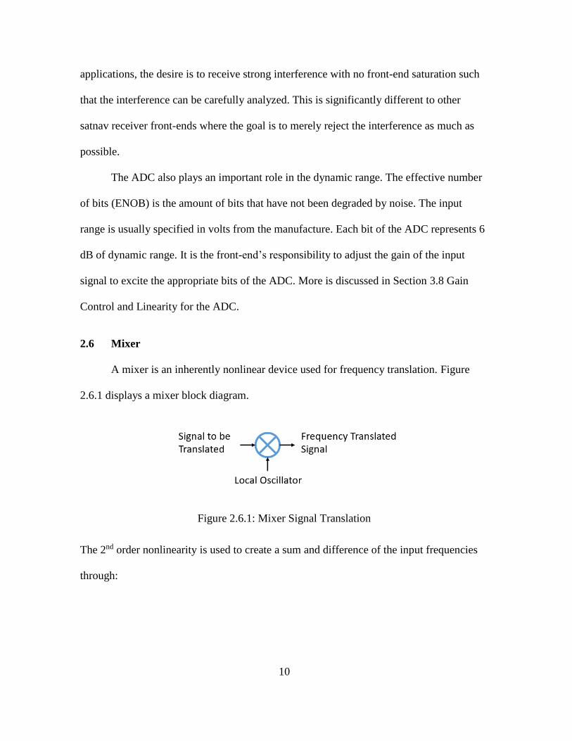
A mixer is an inherently nonlinear device used for frequency translation. Figure
2.6.1 displays a mixer block diagram.
Figure 2.6.1: Mixer Signal Translation
The 2nd order nonlinearity is used to create a sum and difference of the input frequencies
through:
11
𝑓𝑜𝑢𝑡 = 𝑓1 ∓ 𝑓2. (12)
A receiver architecture needs to mix the desired frequency at RF to an intermediate
frequency (IF) where it is sampled and quantized by an ADC. A mixer is usually defined
by its insertion loss and noise figure. Insertion loss is the amount of degradation to the
signal power [6].
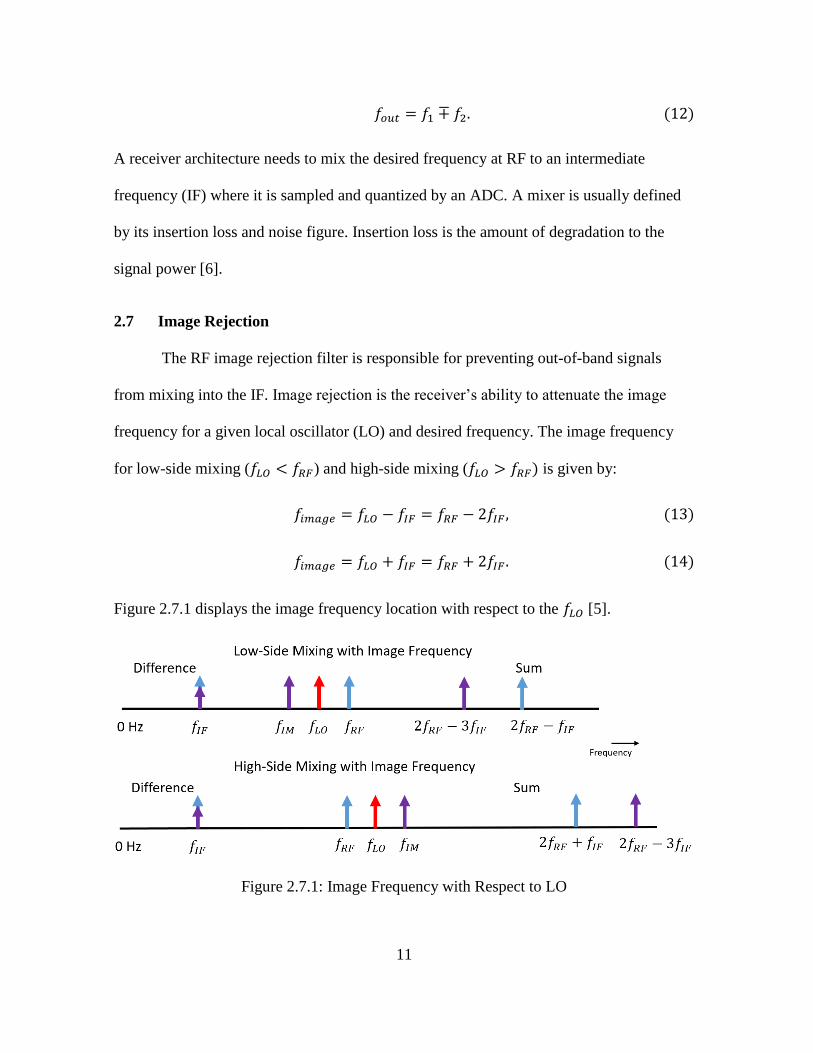
2.7 Image Rejection
The RF image rejection filter is responsible for preventing out-of-band signals
from mixing into the IF. Image rejection is the receiver’s ability to attenuate the image
frequency for a given local oscillator (LO) and desired frequency. The image frequency
for low-side mixing (𝑓𝐿𝑂 < 𝑓𝑅𝐹) and high-side mixing (𝑓𝐿𝑂 > 𝑓𝑅𝐹) is given by:
𝑓𝑖𝑚𝑎𝑔𝑒 = 𝑓𝐿𝑂 − 𝑓𝐼𝐹 = 𝑓𝑅𝐹 − 2𝑓𝐼𝐹 , (13)
𝑓𝑖𝑚𝑎𝑔𝑒 = 𝑓𝐿𝑂 + 𝑓𝐼𝐹 = 𝑓𝑅𝐹 + 2𝑓𝐼𝐹 . (14)
Figure 2.7.1 displays the image frequency location with respect to the 𝑓𝐿𝑂 [5].
Figure 2.7.1: Image Frequency with Respect to LO

12
The image rejection filter’s purpose is to attenuate the image frequency. This prevents
energy from the image frequency from being down converted into the 𝑓𝐼𝐹 .
An image rejection mixer is a technique that some receivers use to remove the need for an
image rejection filter. An image rejection mixer uses 𝑓𝐿𝑂 = 𝑓𝑅𝐹.
2.8 Selectivity
Selectivity is the receiver’s ability to isolate a desired signal at a given frequency
while rejecting out-of-band interference. Spurs generated by the FSPLL can mix-in
outside interference into the passband. Phase noise from the FSPLL will transfer onto any
interfering signals, degrading SNR. Harmonics generated by the nonlinearities of active
components can mix-in unwanted out-of-band interference [6].
2.9 Receiver Architectures
The choice of receiver architecture is dictated by acceptable performance,
implementation, complexity, size, weight, power consumption and cost. Performance is
the most important deciding factor in the design process of a high-fidelity satnav signal
monitoring front-end. Power consumption and size of the front-end is the next most
significant concern. The receiver’s sensitivity, selectivity, image rejection, frequency
planning and generation, dynamic range, and linearity are the major performance
parameters that drive the requirements of the front-end.
Frequency planning and generation are dictated by the receiver architecture and
performance of RF components that are available to the designer. The designer has to
make tradeoffs between performance, size, weight, and cost. The biggest design hurdles
13
lie in the LO generation for down conversion and sampling. Limiting spurs and phase
noise on the LO is fundamental to the performance of the receiver.
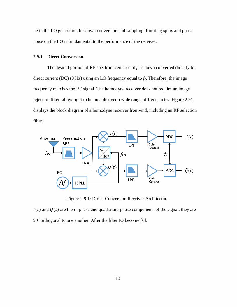
2.9.1 Direct Conversion
The desired portion of RF spectrum centered at fc is down converted directly to
direct current (DC) (0 Hz) using an LO frequency equal to fc. Therefore, the image
frequency matches the RF signal. The homodyne receiver does not require an image
rejection filter, allowing it to be tunable over a wide range of frequencies. Figure 2.91
displays the block diagram of a homodyne receiver front-end, including an RF selection
filter.
Figure 2.9.1: Direct Conversion Receiver Architecture
𝐼(𝑡) and 𝑄(𝑡) are the in-phase and quadrature-phase components of the signal; they are
900 orthogonal to one another. After the filter IQ become [6]:

14
𝐼(𝑡) =1
2𝐼(𝑡) cos(𝜃(𝑡)) +
1
2𝑄(𝑡) sin(𝜃(𝑡)), (15)
(𝑡) =1
2𝐼(𝑡) sin(𝜃(𝑡)) +
1
2𝑄(𝑡) cos(𝜃(𝑡)). (16)
If there is insufficient isolation between the LO and RF signal paths, then the LO
may couple onto the RF input and mix with itself creating a large DC signal at baseband.
The LO may even leak into the input of the LNA, get amplified, and then mix with itself
down to DC. This degradation is particularly present when the LNA, mixer, and FSPLL
are integrated onto the same semiconductor substrate because high levels of isolation are
challenging to achieve on-chip. This is displayed in Figure 2.9.2.
Figure 2.9.2: LO to RF Isolation at the Mixer
Similarly, if a strong interfering signal is present on the RF input at the mixer, it may
couple over to the LO input if the mixer has poor RF-LO isolation. The interfering signal
will then mix itself down to DC. A large DC signal after the mixer can saturate amplifiers
and the ADC [6]. Low frequency phase noise or flicker noise can degrade baseband
signals close to DC [6]. Flicker phase noise is discussed in Section 2.10.
15
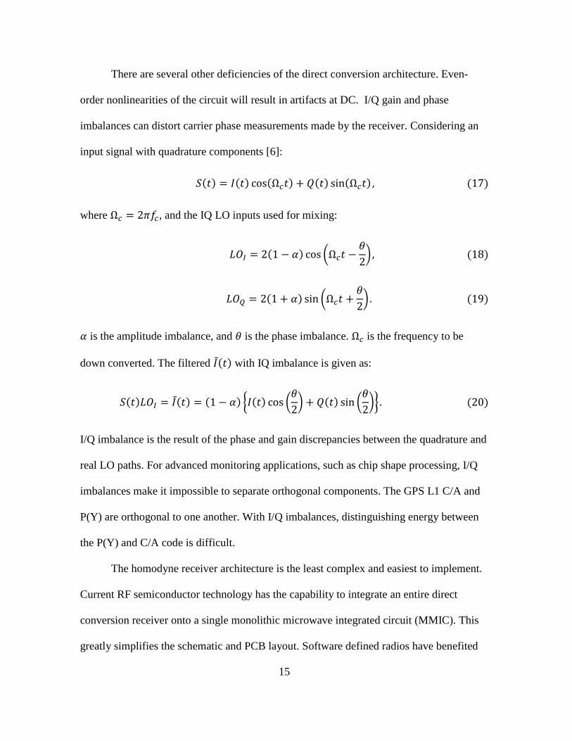
There are several other deficiencies of the direct conversion architecture. Even-
order nonlinearities of the circuit will result in artifacts at DC. I/Q gain and phase
imbalances can distort carrier phase measurements made by the receiver. Considering an
input signal with quadrature components [6]:
𝑆(𝑡) = 𝐼(𝑡) cos(Ω𝑐𝑡) + 𝑄(𝑡) sin(Ω𝑐𝑡), (17)
where Ω𝑐 = 2𝜋𝑓𝑐, and the IQ LO inputs used for mixing:
𝐿𝑂𝐼 = 2(1 − 𝛼) cos (Ω𝑐𝑡 −𝜃
2), (18)
𝐿𝑂𝑄 = 2(1 + 𝛼) sin (Ω𝑐𝑡 +𝜃
2). (19)
𝛼 is the amplitude imbalance, and 𝜃 is the phase imbalance. Ω𝑐 is the frequency to be
down converted. The filtered 𝐼(𝑡) with IQ imbalance is given as:
𝑆(𝑡)𝐿𝑂𝐼 = 𝐼(𝑡) = (1 − 𝛼) 𝐼(𝑡) cos (𝜃
2) + 𝑄(𝑡) sin (
𝜃
2). (20)
I/Q imbalance is the result of the phase and gain discrepancies between the quadrature and
real LO paths. For advanced monitoring applications, such as chip shape processing, I/Q
imbalances make it impossible to separate orthogonal components. The GPS L1 C/A and
P(Y) are orthogonal to one another. With I/Q imbalances, distinguishing energy between
the P(Y) and C/A code is difficult.
The homodyne receiver architecture is the least complex and easiest to implement.
Current RF semiconductor technology has the capability to integrate an entire direct
conversion receiver onto a single monolithic microwave integrated circuit (MMIC). This
greatly simplifies the schematic and PCB layout. Software defined radios have benefited

16
enormously from these ICs due to their flexible band selectivity, high sample rate, and low
power. However, they are inadequate for high-fidelity monitoring due to the reasons
described above.
2.9.2 Direct RF Sampling
The direct RF sampling receiver architecture requires the least number of analog
components. Rather than down converting the desired RF signal, a high-speed ADC with a
high analog input bandwidth samples the signal directly at RF. For multi-frequency
receivers there would be digital channelizers and band limiting processing to get
equivalent functionality of an analog-heavy architecture. There are stringent requirements
for the phase noise performance for the sample clock [7]. Figure 2.9.3 displays the RF-
sampling architecture.
Figure 2.9.3: Direct RF Sampling Receiver Architecture
This architecture requires approximately 100 dB of gain at L-Band frequencies to amplify
the thermal noise power of GNSS bands to the required minimum ADC input level. Since
all this amplification must be done at RF, high input/output isolation is necessary to
prevent feedback oscillation. The high gain differential must be physically separated to
17
achieve this isolation, thus greatly increasing the size of the front-end. Furthermore, high
speed ADCs consume large amounts of power and produces large amounts of data.
Intensive amounts of digital processing are then required to filter, decimate, and
(optionally) store the data – further increasing power and cost.
Due to power consumption and physical size of the direct RF sampling receiver, it
is a less preferable architecture for multi-element arrays.
2.9.3 Superheterodyne Receiver with Bandpass Sampling
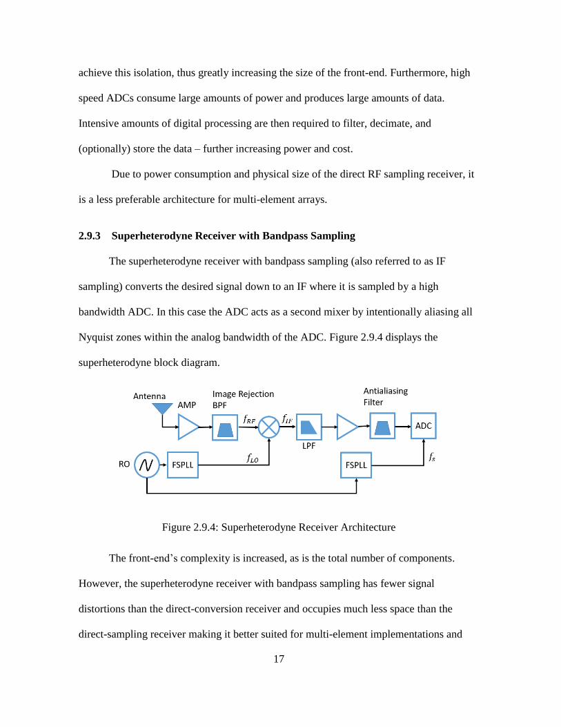
The superheterodyne receiver with bandpass sampling (also referred to as IF
sampling) converts the desired signal down to an IF where it is sampled by a high
bandwidth ADC. In this case the ADC acts as a second mixer by intentionally aliasing all
Nyquist zones within the analog bandwidth of the ADC. Figure 2.9.4 displays the
superheterodyne block diagram.
Figure 2.9.4: Superheterodyne Receiver Architecture
The front-end’s complexity is increased, as is the total number of components.
However, the superheterodyne receiver with bandpass sampling has fewer signal
distortions than the direct-conversion receiver and occupies much less space than the
direct-sampling receiver making it better suited for multi-element implementations and
18
satnav signal quality monitoring and timing applications. The superheterodyne receiver is
free from I/Q gain and phase imbalances because the signal is real sampled, and the
conversion to baseband I/Q happens digitally.
In this architecture, the RF image rejection filter must attenuate any frequency
content at the image frequency to keep it from being mixed onto the IF frequency. The
phase noise and spurs of the FSPLL can degrade the satnav signal and limit the pre-
detection integration time [2] and is discussed in Section 2.11. The choice of IF frequency
and LO frequency are important to the performance of the receiver. By having a higher IF
frequency, and thus a lower LO frequency for low-side mixing, there is greater separation
of the image frequency to the RF frequency. This is an enormous benefit for the
requirements of the RF image rejection filter. By increasing the distance between the RF
and image frequency, the image rejection filter does not need to have a steep response, and
can be a lower Q. However, having a higher frequency at IF can be a challenge to filter
and match. Filters at a higher IF are more difficult to design due to parasitics of the
components and lower Q factors.
2.10 Reference Oscillator
The output of the FSPLL is phase locked to the RO. The RO is essentially
multiplied and divided in a closed loop to obtain a desired frequency. Any frequency
offset or drift of the RO will manifest itself in the FSPLL’s frequency and will need to be
tracked by the receiver’s satnav signal carrier tracking loops. Crystal ROs used in satnav
receivers typically have good short-term frequency stability but drift over the long term.
Oven controlled crystal oscillators (OCXOs) extend this short-term stability by
19
minimizing temperature variations – making them more desirable for instrumentation
satnav receivers which require long pre-detection integration times.
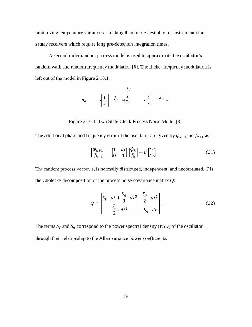
A second-order random process model is used to approximate the oscillator’s
random walk and random frequency modulation [8]. The flicker frequency modulation is
left out of the model in Figure 2.10.1.
Figure 2.10.1: Two State Clock Process Noise Model [8]
The additional phase and frequency error of the oscillator are given by 𝜙𝑘+1and 𝑓𝑘+1 as:
[𝜙𝑘+1
𝑓𝑘+1] = [
1 𝑑𝑡0 1
] [𝜙𝑘
𝑓𝑘] + 𝐶 [
𝜀1
𝜀2]. (21)
The random process vector, ε, is normally distributed, independent, and uncorrelated. C is
the Cholesky decomposition of the process noise covariance matrix Q:
𝑄 = [𝑆𝑓 ⋅ 𝑑𝑡 +
𝑆𝑔
3⋅ 𝑑𝑡3
𝑆𝑔
2⋅ 𝑑𝑡2
𝑆𝑔
2⋅ 𝑑𝑡2 𝑆𝑔 ⋅ 𝑑𝑡
]. (22)
The terms 𝑆𝑓 and 𝑆𝑔 correspond to the power spectral density (PSD) of the oscillator
through their relationship to the Allan variance power coefficients:
20
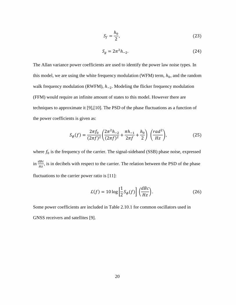
𝑆𝑓 =ℎ0
2, (23)
𝑆𝑔 = 2𝜋2ℎ−2. (24)
The Allan variance power coefficients are used to identify the power law noise types. In
this model, we are using the white frequency modulation (WFM) term, ℎ0, and the random
walk frequency modulation (RWFM), ℎ−2. Modeling the flicker frequency modulation
(FFM) would require an infinite amount of states to this model. However there are
techniques to approximate it [9],[10]. The PSD of the phase fluctuations as a function of
the power coefficients is given as:
𝑆𝜙(𝑓) =2𝜋𝑓0
(2𝜋𝑓)2(
2𝜋2ℎ−2
(2𝜋𝑓)2+
𝜋ℎ−1
2𝜋𝑓+
ℎ0
2) (
𝑟𝑎𝑑2
𝐻𝑧), (25)
where 𝑓0 is the frequency of the carrier. The signal-sideband (SSB) phase noise, expressed
in 𝑑𝐵𝑐
𝐻𝑧, is in decibels with respect to the carrier. The relation between the PSD of the phase
fluctuations to the carrier power ratio is [11]:
ℒ(𝑓) = 10 log [1
2𝑆𝜙(𝑓)] (
𝑑𝐵𝑐
𝐻𝑧) . (26)
Some power coefficients are included in Table 2.10.1 for common oscillators used in
GNSS receivers and satellites [9].

21
Table 2.10.1: Allan Variance Power Coefficients for Typical Oscillators
Oscillator WFM ℎ0 Flicker ℎ−1 RWFM ℎ−2
Standard Quartz 2E-19 7E-21 2E-20
TCXO 1E-21 1E-20 2E-20
OCXO1 8E-20 2E-21 4E-23
OCXO2 2.51E-26 2.51E-23 2.51E-22
Rubidium 1E-19 1E-22 1.3E-26
Cesium1 1E-19 1E-25 2E-32
Cesium2 2E-20 7E-23 4E-29
The power law coefficients are used to calculate the PSD of OCXO1 using (25) (26) is
shown in Figure 2.10.2.
Figure 2.10.2: SSB Calculated Phase Noise of OCXO1
The Allan variance curve can be calculated from the power coefficients from a particular
oscillator through [11]:
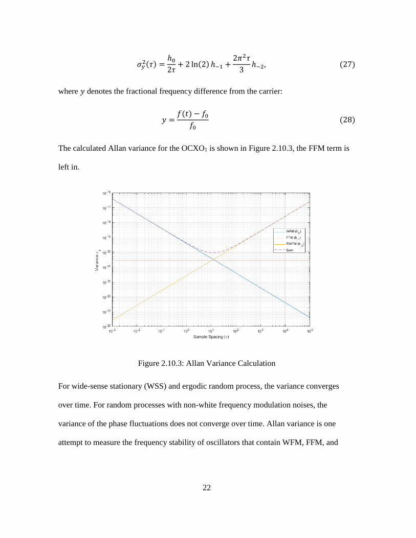
22
𝜎𝑦2(𝜏) =
ℎ0
2𝜏+ 2 ln(2) ℎ−1 +
2𝜋2𝜏
3ℎ−2, (27)
where 𝑦 denotes the fractional frequency difference from the carrier:
𝑦 =𝑓(𝑡) − 𝑓0
𝑓0 (28)
The calculated Allan variance for the OCXO1 is shown in Figure 2.10.3, the FFM term is
left in.
Figure 2.10.3: Allan Variance Calculation
For wide-sense stationary (WSS) and ergodic random process, the variance converges
over time. For random processes with non-white frequency modulation noises, the
variance of the phase fluctuations does not converge over time. Allan variance is one
attempt to measure the frequency stability of oscillators that contain WFM, FFM, and

23
RWFM noise. The overlapping Allan variance is the most common technique and is given
as [11],[8]:
𝜎𝑦2(𝜏) =
1
2(𝑁 − 2𝑚)𝜏2, (29)
where x(t) is the time error given as 𝜙(𝑡)
2𝜋𝑓0. Upon the discrete simulation of the clock model
using the Allan Variance power coefficients from the OCXO1 we show that the simulation
matched the variance calculations from (19) as displayed in Figure 2.10.4. Note, however,
that the FFM plays little effect for OCXO1.
Figure 2.10.4: Simulated vs. Calculated Allan Variance
2.11 Frequency Synthesizer Phase Locked Loop
An integer-N charge pump phase locked loop (PLL) with integrated voltage-
controlled oscillator (VCO) circuit diagram is displayed in Figure 2.11.1. To control the
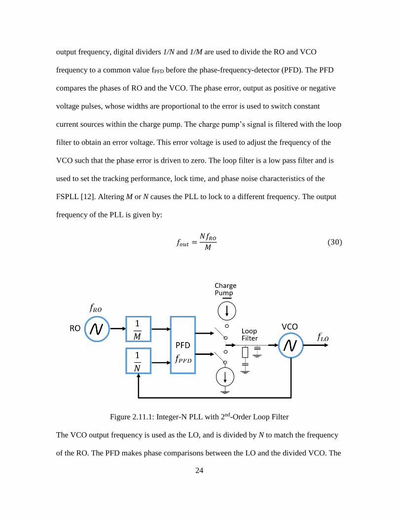
24
output frequency, digital dividers 1/N and 1/M are used to divide the RO and VCO
frequency to a common value fPFD before the phase-frequency-detector (PFD). The PFD
compares the phases of RO and the VCO. The phase error, output as positive or negative
voltage pulses, whose widths are proportional to the error is used to switch constant
current sources within the charge pump. The charge pump’s signal is filtered with the loop
filter to obtain an error voltage. This error voltage is used to adjust the frequency of the
VCO such that the phase error is driven to zero. The loop filter is a low pass filter and is
used to set the tracking performance, lock time, and phase noise characteristics of the
FSPLL [12]. Altering M or N causes the PLL to lock to a different frequency. The output
frequency of the PLL is given by:
𝑓𝑜𝑢𝑡 =𝑁𝑓𝑅𝑂
𝑀 (30)
Figure 2.11.1: Integer-N PLL with 2nd-Order Loop Filter
The VCO output frequency is used as the LO, and is divided by N to match the frequency
of the RO. The PFD makes phase comparisons between the LO and the divided VCO. The
25
PFD makes comparisons at a rate of 𝑓𝑃𝐹𝐷. The PFD control signals are then converted into
a control current by the charge pump and filtered by the loop filter before controlling the
VCO.
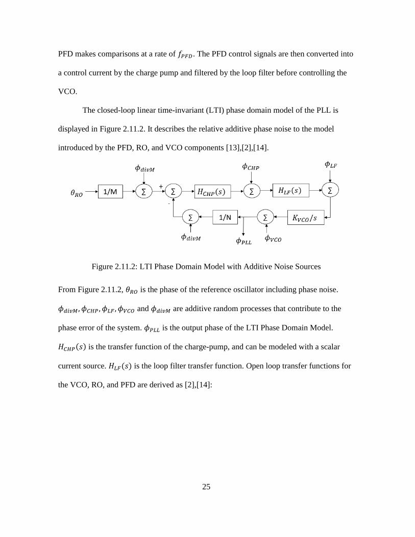
The closed-loop linear time-invariant (LTI) phase domain model of the PLL is
displayed in Figure 2.11.2. It describes the relative additive phase noise to the model
introduced by the PFD, RO, and VCO components [13],[2],[14].
Figure 2.11.2: LTI Phase Domain Model with Additive Noise Sources
From Figure 2.11.2, 𝜃𝑅𝑂 is the phase of the reference oscillator including phase noise.
𝜙𝑑𝑖𝑣𝑀 , 𝜙𝐶𝐻𝑃, 𝜙𝐿𝐹 , 𝜙𝑉𝐶𝑂 and 𝜙𝑑𝑖𝑣𝑀 are additive random processes that contribute to the
phase error of the system. 𝜙𝑃𝐿𝐿 is the output phase of the LTI Phase Domain Model.
𝐻𝐶𝐻𝑃(𝑠) is the transfer function of the charge-pump, and can be modeled with a scalar
current source. 𝐻𝐿𝐹(𝑠) is the loop filter transfer function. Open loop transfer functions for
the VCO, RO, and PFD are derived as [2],[14]:
26
𝐻𝑉𝐶𝑂(𝑠) =𝑠𝑁
𝑠𝑁 + 𝐼𝑝𝐾𝑉𝐶𝑂𝐻𝐿𝐹(𝑠), (31)
𝐻𝑅𝑂(𝑠) =𝑁𝐼𝑝𝐾𝑉𝐶𝑂𝐻𝐿𝐹(𝑠)
𝑀 (𝑠𝑁 + 𝐼𝑝𝐾𝑉𝐶𝑂𝐻𝐿𝐹(𝑠)), (32)
𝐻𝑃𝐹𝐷(𝑠) =2𝜋𝑁𝐾𝑉𝐶𝑂𝐻𝐿𝐹(𝑠)
𝑠𝑁 + 𝐼𝑝𝐾𝑉𝐶𝑂𝐻𝐿𝐹(𝑠), (33)
where the loop filter transfer function is 𝐻𝐿𝐹(𝑠), and s is the complex frequency parameter
of the system. M and N are the dividers for matching the reference’s frequency to the
VCO’s frequency before the PFD. 𝐼𝑝 (A) is the charge pump current, this is typically a
programmable value for modern FSPLLs. 𝐾𝑉𝐶𝑂 is the gain of the VCO expressed in Hz/V.
The loop filter transfer function, 𝐻𝐿𝐹(𝑠), high passes the phase noise from the VCO and
low passes the phase noise from the RO to the output. The total PSD of the FSPLL can be
calculated through [2]:
𝑃𝜙(𝑓) = 𝑃𝜙𝑉𝐶𝑂(𝑓) + 𝑃𝜙𝑅𝑂(𝑓) + 𝑃𝜙𝑃𝐹𝐷(𝑓), (34)
𝑃𝜙𝑉𝐶𝑂(𝑓) = |𝐻𝑉𝐶𝑂(𝑓)|2|𝐻𝑖𝑖(𝑓)|24𝜋2𝑓𝑐,𝑣𝑐𝑜2 𝑐𝑤,𝑣𝑐𝑜, (35)
𝑃𝜙𝑅𝑂(𝑓) = |𝐻𝑅𝑂(𝑓)|2|𝐻𝑖𝑖(𝑓)|24𝜋2𝑓𝑐,𝑟𝑜2 𝑐𝑤,𝑟𝑜, (36)
𝑃𝜙𝑃𝐹𝐷(𝑓) = |𝐻𝑃𝐹𝐷(𝑓)|2𝑐𝑤,𝑝𝑓𝑑. (37)
𝐻𝑖𝑖(𝑓) is an ideal integrator transfer function. 𝑓𝑐,𝑣𝑐𝑜, and 𝑓𝑐,𝑟𝑜 are the frequencies of the
VCO and RO respectively. 𝑐𝑤,𝑣𝑐𝑜 and 𝑐𝑤,𝑟𝑜 are spot phase noise models of their respective
devices [2], [13]. The phase noise of the RO is low passed and the phase noise of the VCO
is high passed by the loop filter. Thus, to best minimize the amount of phase noise
27
contributed by the VCO and PFD, the loop filter should have an equivalent bandwidth of
where the VCO phase noise intersects the noise floor of the FSPLL [12]. Passive filters
are ideal for low phase noise applications; a passive component-based second-order
filter’s transfer function is [12]:
𝐻𝐿𝐹(𝑠) =1 + 𝑠𝐶2𝑅2
𝑠(𝐶1 + 𝐶2) [1 + 𝑠 [𝐶1𝐶2𝑅2
𝐶1 + 𝐶2]]
. (38)
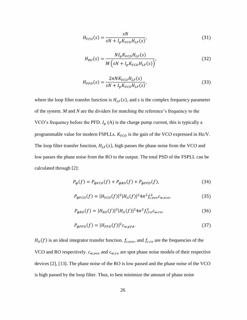
Figure 2.11.3 shows the calculated and measured PSD for the LMX 2582 integrated-VCO
FSPLL IC [15] in its first configuration, which is further discussed in Section 4.4.
Figure 2.11.3: FSPLL Simulated Phase Noise and Measured Phase Noise from LMX 2582
In its 1st Configuration
The model is a close approximation of the phase noise from the LMX2582’s 1st
configuration in Chapter 4.4: Frequency Synthesizer Evaluation. However, this is not
28
adequate to be able to gain detailed insight into vendor-specific devices, or other features
that are not included in the FSPLL model. An instrumentation grade receiver benefits
from the lowest possible phase noise from an FSPLL. Thus, it is more beneficial to the
community to conduct measurements on vendor’s evaluation boards. Vendors also supply
tools to aid frequency synthesizer design for their specific devices, which may provide a
more accurate phase noise model than (26).
Figure 2.11.3 shows that the RO is the greatest contributor to the close-in phase
noise (i.e. phase noise at frequencies < 100 Hz offset from center). The PFD dominates
around 103 to 104 Hz while the VCO is dominant >104 Hz. Of course, the bandwidth of the
loop filter, 𝐻𝐿𝐹(𝑠), determines how the phase noise of the respective devices are passed to
the output.
2.12 Group Delay Variations
Group delay is the derivative of the phase response of a device under test (DUT)
with respect to frequency. It is the time it takes for a wave of a given frequency to
propagate through a DUT:
𝜏𝑔(𝜔) = −𝑑𝜙(𝜔)
𝑑𝜔. (39)
Depending upon the application, group delay can become a problem. If the group
delay variation of a filter is changing due to temperature changes, then the group delay
will change all the pseudoranges by the same amount. This effectively comes out as a
clock error. The position is not affected. The position derivation can be affected for
FDMA signals like GLONASS. Each SV’s signal centered at a different frequency will
29
experience a different delay in the front-end. This will manifest itself as a position error if
the group delay is not accounted for.
Advanced monitoring applications such as chip transition characterization,
otherwise known as “chip-shape” [1], [3], requires minimum group delay variations over
the front-end passband. Delay variations over the passband adds distortions to the signal
that are not characteristic to the satellite. Shorter spreading codes, such as GPS C/A (1023
chips) and GLONASS C/A (511 chips) are most impacted by these group delay variations
due to the wider-spread and overall smaller number of spectral lines in the spreading
code’s PSD that can lead to inter-PRN pseudorange biases [4],[5]. The spacing between
spectral lines of a pseudorange sequence is inversely proportional to the period of the
sequence. As spreading sequences become longer, the group delay variations in the front-
end’s passband becomes less of an issue [16].
2.13 RF Filters for Satnav Instrumentation
There are several types of RF filters that suitable for satnav applications. The
surface acoustic wave (SAW) filter, the cavity filter, distributed element, and the ceramic
cavity filters offer different performance, cost, size, and weight. The SAW filter is the
cheapest and the smallest. Unfortunately, the SAW filter is not appropriate for
instrumentation satnav receivers due to large group delay variations in the passband and
sensitivity to temperature changes. SAW filters offer an excellent brick wall response, but
may not offer enough attenuation in the stopband, especially at higher frequencies. Cavity
filters are the most expensive and offer the best frequency response. However, their large
size and weight does make them ideal for size and weight constrained designs. Distributed
30
element filters can be built onto the PCB substrate but will take up large amounts of space
for L-Band signals. Ceramic cavity filters can be custom ordered and PCB mounted. The
response and group delay variations are consistent over temperature.
The RF filter’s purpose is to select the band of interest and attenuate any out-of-
band interference. The RF filter’s other purpose is image rejection for superheterodyne
receivers. As stated in Section 2.7, group delay variations over the passband of the filter
need to be minimized.
2.14 IF / Antialiasing Filters
The construction of the antialiasing filter prevents outer-band interference from
aliasing into the sampled signal. The filter response shape should have at least 74 dB of
attenuation outside the passband of the filter to prevent the ADC from quantizing outside
interference. This number is derived from the ENOB and dynamic range of the ADC. The
filter also adds its own group delay to the signal that must be minimized. Surface acoustic
wave (SAW) filters may have a brick wall response, but the group delay variations within
the passband can be extreme making them non-ideal for instrumentation-grade satnav
signal monitoring applications [3]. The group delay of SAW filters is also highly
temperature dependent, adding error in advanced timing applications [4]. Specially tuned
inductor-capacitor (LC) filters can have a reasonably flat group delay response in the
passband that does not vary as much as SAW filters over temperature [4]. The drawback is
being able to design a filter with practical LC components that meet the stopband
attenuation, passband width, and reasonably small size. For example, high-Q inductors are
desired to obtain a sharp stopband response. However, the highest realizable Q inductors
31
tend to be air-core types which are much larger in size compared to ferrite-core types. Air-
core inductors are also more sensitive to temperature variations, and have wider variations
on labeled value (i.e. tolerances) due to manufacturing variations.
2.15 Receiver Carrier Tracking Loops and Errors
Tracking loops are used to recover the satnav signal’s parameters. The carrier
tracking loops are responsible for recovering the phase and Doppler of the satnav signal.
Code tracking loops are responsible for recovering the satnav signal’s code phase. From
these raw observables carrier phase and pseudorange measurements can be derived,
respectively [17]. A satnav receiver channel’s carrier tracking loop is displayed in Figure
2.15.1.
Figure 2.15.1: Receiver Carrier Tracking Loop
Thermal noise present on the sampled IF signal results in errors on the phase/frequency
discriminator. The loop filter low pass filters the phase estimates from the discriminator
and steers the replica generator. The thermal noise contributions for a pilot (no data) and
data-containing channel are given as [17]:

32
𝜎𝑡𝑃𝐿𝐿𝑃=
360
2𝜋√
𝐵𝑁
𝐶𝑁𝑅 (𝑑𝑒𝑔𝑠) (40)
𝜎𝑡𝑃𝐿𝐿𝐷=
360
2𝜋√
𝐵𝑁
𝐶𝑁𝑅(1 +
1
2𝑇 ∗ 𝐶𝑁𝑅) (𝑑𝑒𝑔𝑠) (41)
Phase noise produced by the FSPLL, ADC clock, and RO degrade the SNR of the carrier
tracking loops [2], [17], [18]. The phase noise is introduced by the RO and can be
quantified in terms of the Allan deviation of the oscillator, vibration or mechanical stress.
The tracking threshold for the PLL tracking loop for a two-quadrant (Costas)
discriminator for a data channel is [17]:
𝜎𝑃𝐿𝐿𝐷= √𝜎𝑡𝑃𝐿𝐿
2𝐷
+ 𝜎𝑉2 + 𝜃𝐴
2 +𝜃𝑒
3≤ 15𝑜 (42)
where 𝜎𝑉2 is the Allan variance induced phase noise of the RO and 𝜃𝐴
2 is the vibration-
induced phase noise. The vibration induced phase noise is treated as negligible in this
study since satnav monitoring applications are assumed to be stationary. The contributions
of the Allan variance to the phase estimate is given as [18],[5],[19],[20]:
𝜎𝑉2 =
1
2𝜋∫ 𝑆𝑣(𝜔)|1 − 𝐻(𝜔)|2𝑑𝜔.
∞
0
(43)
𝑆𝑣(𝜔) is the oscillator phase noise PSD, modeled by the Allan variance clock parameters.
|1 − 𝐻(𝜔)|2 is the inverse magnitude response of the carrier tracking loop filter and is
dependent upon the loop order and noise bandwidth. It is also defined as [18]:
33
|1 − 𝐻(𝜔)|2 =𝜔2𝑛
𝜔𝐿2𝑛 + 𝜔2𝑛
, (44)
where n is the loop order and 𝜔𝐿2𝑛 is dependent upon the loop filter values. Typical values
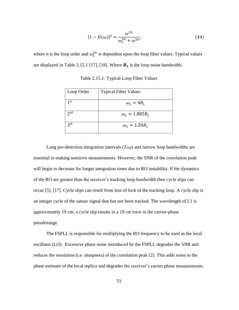
are displayed in Table 2.15.1 [17], [18]. Where 𝑩𝑳 is the loop noise bandwidth.
Table 2.15.1: Typical Loop Filter Values
Loop Order Typical Filter Values
1st 𝜔𝐿 = 4𝐵𝐿
2nd 𝜔𝐿 = 1.885𝐵𝐿
3rd 𝜔𝐿 = 1.20𝐵𝐿
Long pre-detection integration intervals (TPDI) and narrow loop bandwidths are
essential to making sensitive measurements. However, the SNR of the correlation peak
will begin to decrease for longer integration times due to RO instability. If the dynamics
of the RO are greater than the receiver’s tracking loop bandwidth then cycle slips can
occur [5], [17]. Cycle slips can result from loss of lock of the tracking loop. A cycle slip is
an integer cycle of the satnav signal that has not been tracked. The wavelength of L1 is
approximately 19 cm; a cycle slip results in a 19 cm error in the carrier-phase
pseudorange.
The FSPLL is responsible for multiplying the RO frequency to be used as the local
oscillator (LO). Excessive phase noise introduced by the FSPLL degrades the SNR and
reduces the resolution (i.e. sharpness) of the correlation peak [2]. This adds noise to the
phase estimate of the local replica and degrades the receiver’s carrier phase measurements.
34
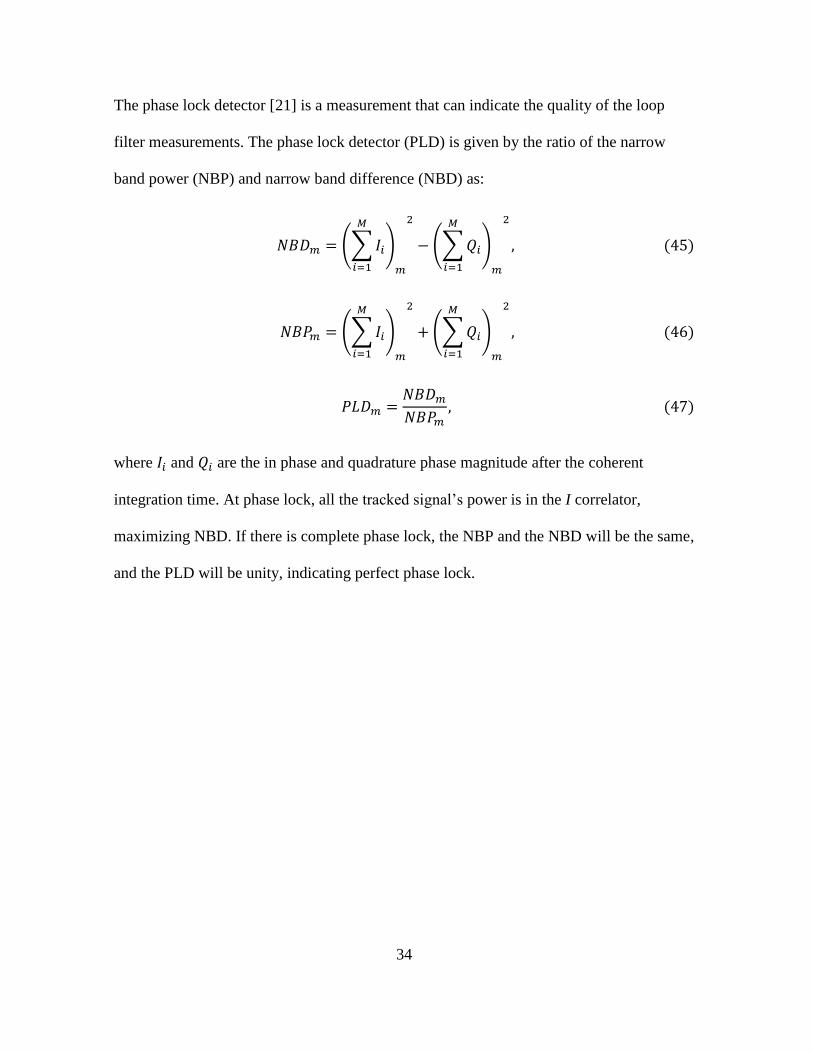
The phase lock detector [21] is a measurement that can indicate the quality of the loop
filter measurements. The phase lock detector (PLD) is given by the ratio of the narrow
band power (NBP) and narrow band difference (NBD) as:
𝑁𝐵𝐷𝑚 = (∑ 𝐼𝑖
𝑀
𝑖=1
)
𝑚
2
− (∑ 𝑄𝑖
𝑀
𝑖=1
)
𝑚
2
, (45)
𝑁𝐵𝑃𝑚 = (∑ 𝐼𝑖
𝑀
𝑖=1
)
𝑚
2
+ (∑ 𝑄𝑖
𝑀
𝑖=1
)
𝑚
2
, (46)
𝑃𝐿𝐷𝑚 =𝑁𝐵𝐷𝑚
𝑁𝐵𝑃𝑚, (47)
where 𝐼𝑖 and 𝑄𝑖 are the in phase and quadrature phase magnitude after the coherent
integration time. At phase lock, all the tracked signal’s power is in the I correlator,
maximizing NBD. If there is complete phase lock, the NBP and the NBD will be the same,
and the PLD will be unity, indicating perfect phase lock.
35
III. Methodology
3.1 Chapter Overview
The aim of this thesis is to design, fabricate, and test a satnav front-end receiver
capable of instrumentation grade characterization of satnav signals. The front-end of any
RF receiver is responsible for frequency selectivity, frequency translation, and
digitization. A high-fidelity front end preserves the original signal characteristics and
contributes as little noise, distortion and colorization as possible given the specified
dynamic range of operation. The front-end design shall also support multi-element
antenna arrays for obtaining spatial and polarization information about an environment.
An instrumentation satnav receiver must be able to make high fidelity
measurements under the duress of strong interference and signal fading. The satnav
receiver is designed to handle 100 dB Jamming-to-Signal ratio (J/S) while preserving
linearity of the components in the signal path. Filters at RF and IF frequencies contribute
group delay distortions to the received satnav signal. Group delay variations causes inter-
pseudorange biases for short PRN codes and also contribute chip-shape deformations to
the nominal satnav signal [4]. Satnav signals from the USAF’s GPS are broadcast in three
separate bands, L1, L2, and L5. The methodology for an L1 RF front-end is covered here.
The same procedure will apply to the other bands. The key focus points of the design
methodology are:
Frequency plan with +50 MHz of usable bandwidth for wideband satnav signal
monitoring.
Minimal group delay variations over the passband contributed by the filters.

36
Configuring a FSPLL for minimal phase noise and spurs.
Gain control and preserving linearity of the front-end.
3.2 Receiver Architectures
The first task in designing a satnav receiver front-end is to derive the frequency
plan. There are several receiver architectures used in satnav receiver front-ends: direct-
sampling, direct-conversion, and superheterodyne.
The superheterodyne receiver architecture with bandpass sampling was chosen for
superior selectivity, linearity, and sensitivity over the direct conversion receiver. The
superheterodyne may be more complex than the direct sampling receivers, however, the
superheterodyne consumes less power and space. Power and space consumption is
important for employing multielement antenna arrays.
The next step in defining the frequency plan is to conduct a market assessment of
available RF parts from major industry vendors. In building a satnav receiver with PCB
surface mount components we benefit from the wide range of available parts that target
the many wireless communication industries. Perhaps the most important part to select
first is the analog-to-digital converter (ADC), as the sampling rate will drive the frequency
plan for the receiver.
3.3 Analog to Digital Converter
For multi-element arrays, to perform digital beamforming, each antenna needs to be
sampled coherently. An ADC with multiple channels, high sample rate, high analog input
bandwidth, and high dynamic range is best suited for an instrumentation satnav receiver.
Analog Device’s AD9681 [22] has eight ADC channels, a sample rate of 125 MSPS per
37
channel, and 14 bits of dynamic range integrated into a single IC package. By integrating
all of the ADC channels into a single package, each input channel can be coherently
sampled, greatly reducing design complexity. The AD 9681 has an analog input of 650
MHz allowing for subsampling in higher Nyquist zones.
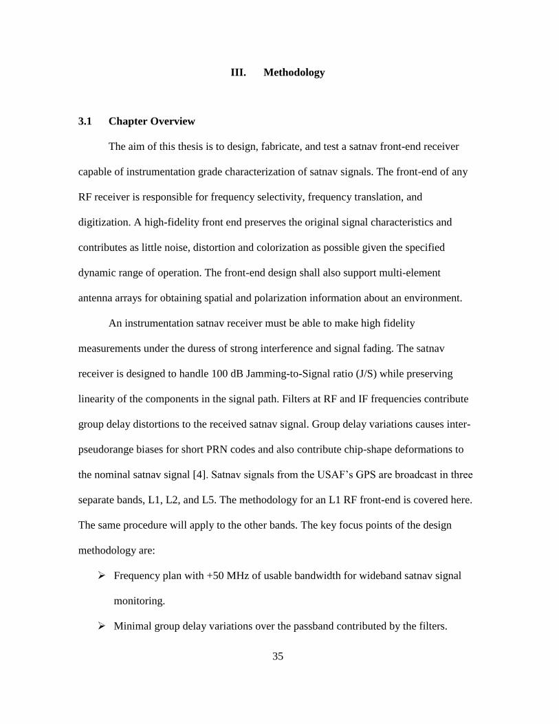
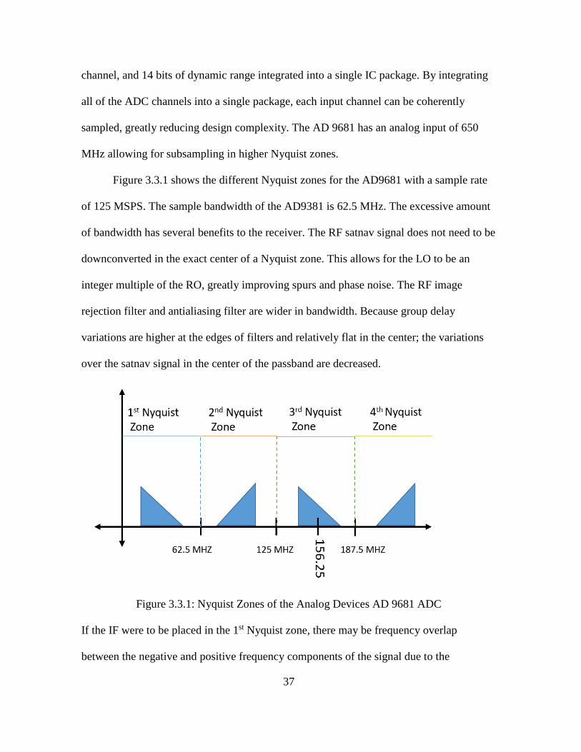
Figure 3.3.1 shows the different Nyquist zones for the AD9681 with a sample rate
of 125 MSPS. The sample bandwidth of the AD9381 is 62.5 MHz. The excessive amount
of bandwidth has several benefits to the receiver. The RF satnav signal does not need to be
downconverted in the exact center of a Nyquist zone. This allows for the LO to be an
integer multiple of the RO, greatly improving spurs and phase noise. The RF image
rejection filter and antialiasing filter are wider in bandwidth. Because group delay
variations are higher at the edges of filters and relatively flat in the center; the variations
over the satnav signal in the center of the passband are decreased.
Figure 3.3.1: Nyquist Zones of the Analog Devices AD 9681 ADC
If the IF were to be placed in the 1st Nyquist zone, there may be frequency overlap
between the negative and positive frequency components of the signal due to the
38
performance of the RF image rejection filters. Frequency content overlap would be
detrimental to the SNR of the satnav signal. Figure 3.3.2 displays how the antialiasing
filter and RF filter may inadequately prevent contamination between the positive and
negative frequency components of the signal. Shown in orange is the filter response of the
antialiasing filter, and in blue, the response of the RF filter.
Figure 3.3.2: 1st Nyquist Zone Frequency Overlap
The third Nyquist zone was chosen as the IF due to having over 200 MHz of separation
from the translated negative frequency. Having a higher IF frequency also increases the
distance between the desired signal and its image frequency. The image frequency is
centered at 1269 MHz. By having a larger separation between the desired signal and the
image, the response of the RF filter does not need to have a brick wall response.
The 3rd Nyquist zone is centered at 156.25 MHz. When sampled, the Nyquist
zones are aliased into the quantized signal. A 50 MHz antialiasing BPF is needed for the
3rd Nyquist zone to prevent outside interference from aliasing into the sampled signal. A
50 MHz filter gives 6.25 MHz for the roll-off of the filter; this ensures adequate
attenuation of out-of-band interference. A wider bandwidth filter allows for a flatter group

39
delay response in the center of the filter. Figure 3.3.3 displays the down converted signal
in blue and the 50 MHz antialiasing filter in orange.
Figure 3.3.3: 3rd Nyquist Zone Frequency Response
To convert the L1 center frequency of 1575.42 MHz down to 156.25 MHz an LO of
1419.17 MHz is needed. However, as we will see in Section 3.7, synthesizing the exact
frequency of 1419.17 MHz can increase the amount of phase noise from the FSPLL.
Instead, an LO 1420 MHz is used for down conversion because it is an integer multiple of
the RO (10 MHz). Figure 3.3.4 displays the frequency plan for L1.
Figure 3.3.4: Frequency Plan of the Receiver Front-End

40
To down convert the L2 center frequency of 1227.60 MHz to 156.25 MHz an LO
of 1071.35 MHz is needed. However, using an LO frequency of 1070 MHz from the
frequency synthesizer will result in better phase noise performance. To down convert the
L5 center frequency of 1176.45 MHz to 156.25 MHz a LO of 1020.20 MHz is needed. To
improve phase noise, a LO of 1020 MHz can be used. The AD9681 operates off a 1000
MHz clock that is divided internally to a sampling frequency of 125 MHz.
The ADC has 14 bits of dynamic range. This equates to 84.3 dB of dynamic range
(6 dB per bit). However, the two least significant bits are dominated by ADC background
noise, giving an effective 72 dB of dynamic range. This will be important in the later
design of some components. For full scale quantization, the ADC can handle up to 2 V
peak-to-peak. The load is 50 Ω. The maximum input power required for full-scale
excitation of the ADC is given by:
(1
√2)
2
(1
50) = 0.01 𝑊 = −20 𝑑𝐵𝑊 = 10 𝑑𝐵𝑚. (48)
3.4 Bandpass Antialiasing Filter
The construction of the antialiasing filter prevents outer-band interference from
aliasing into the sampled signal. The filter response shape should have at least 74 dB of
attenuation outside the passband of the filter to prevent the ADC from quantizing outside
interference. The filter also adds its own group delay variations to the signal that must be
minimized. Specially tuned LC filters can have a flat group delay response in passband
that does not vary over temperature. The drawback is being able to design a filter with
41
realizable LC components that meet the stopband attenuation, group delay, and 3 dB
bandwidth.
Group delay variations will be greatest at the edges of the passband; these
variations are inevitable. The variations at the center of the filter should be as small as
possible to prevent signal deformations. A high sample rate works to our advantage by
allowing for higher bandwidth bandpass filters thus decreasing the amount of group delay
variations over the satnav signal’s bandwidth. Once the IF signal has been sampled and
quantized, a finite impulse response (FIR) filters can be used to compensate for group
delay variations or extract the usable portion of the spectrum. Afterwards the signal can be
decimated to reduce DSP clock speed.
Filter design software exists for designing LC bandpass filters. Keysight Genesys is
one tool that offers a good filter design software. Modeling of the real components’
quality factor (Q), inductance, and parasitics at the designed frequency is difficult because
they are dependent on the individual vendor’s components. Modelithics [23] is a company
that measures the S-parameters of many vendor’s components and sells accurate models
for designers to best utilize them. Genesys has the capability to utilize these models in
their Vendor Part Synthesis (VPS) tool [24]. First the filter is designed using ideal LC
components with high-Q and no parasitics. Next the designer specifies what component
libraries to use. The VPS tool then tries to fit the Modelithics component models to the
ideal LC filter response.
A 50 MHz, 9th order Cauer-Chebyshev minimum inductor filter was designed with
the Genesys filter design software. The low frequency cutoff is 131.25 MHz and the upper
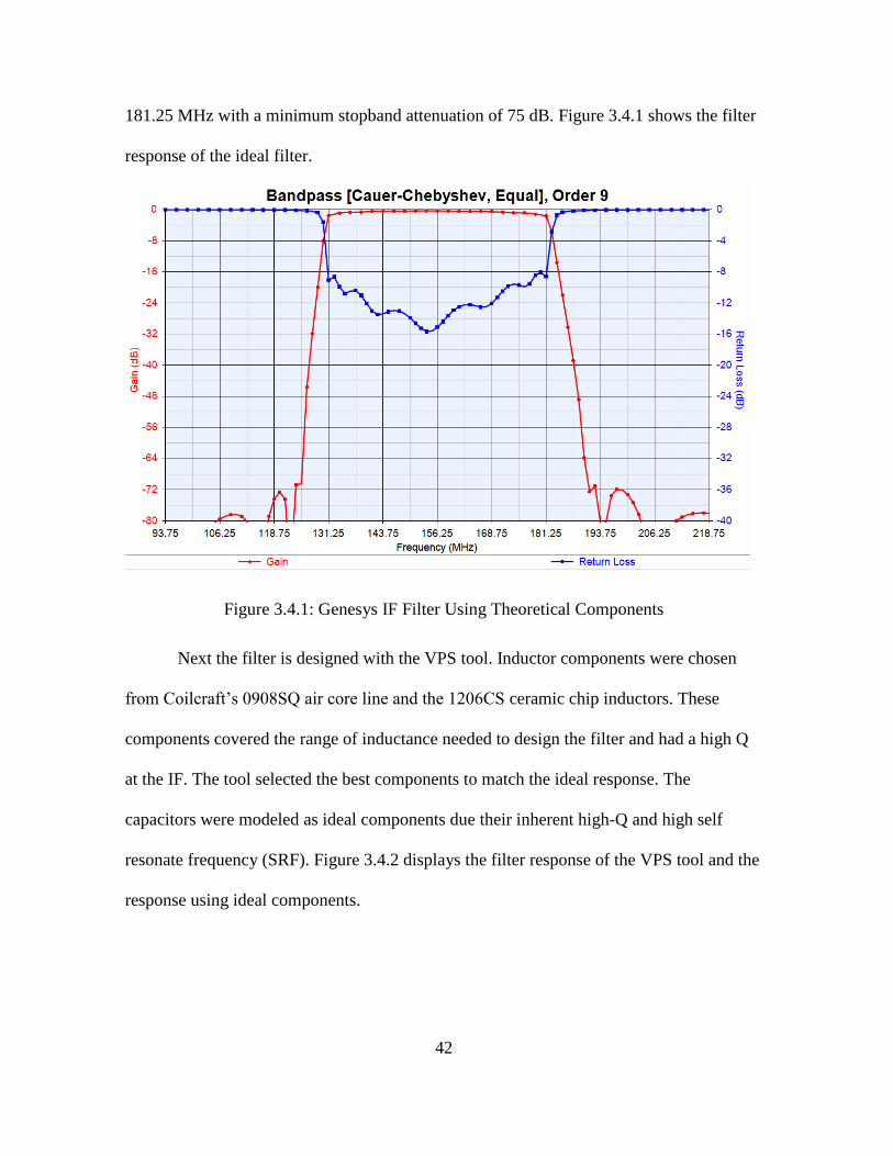
42
181.25 MHz with a minimum stopband attenuation of 75 dB. Figure 3.4.1 shows the filter
response of the ideal filter.
Figure 3.4.1: Genesys IF Filter Using Theoretical Components
Next the filter is designed with the VPS tool. Inductor components were chosen
from Coilcraft’s 0908SQ air core line and the 1206CS ceramic chip inductors. These
components covered the range of inductance needed to design the filter and had a high Q
at the IF. The tool selected the best components to match the ideal response. The
capacitors were modeled as ideal components due their inherent high-Q and high self
resonate frequency (SRF). Figure 3.4.2 displays the filter response of the VPS tool and the
response using ideal components.
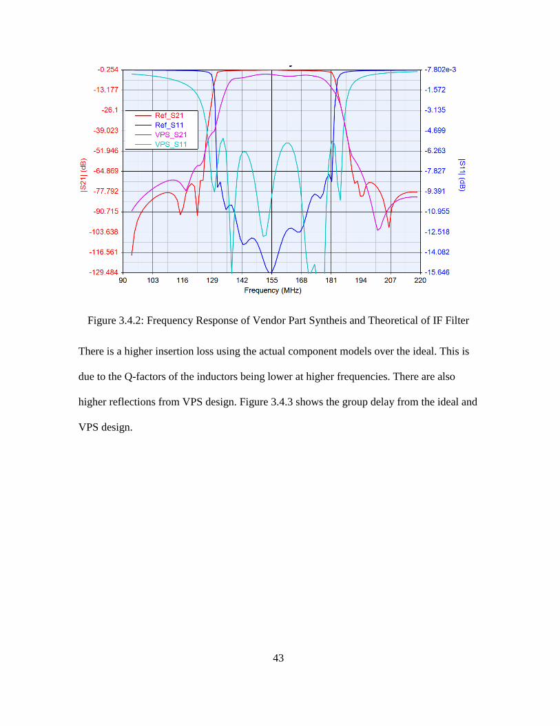
43
Figure 3.4.2: Frequency Response of Vendor Part Syntheis and Theoretical of IF Filter
There is a higher insertion loss using the actual component models over the ideal. This is
due to the Q-factors of the inductors being lower at higher frequencies. There are also
higher reflections from VPS design. Figure 3.4.3 shows the group delay from the ideal and
VPS design.
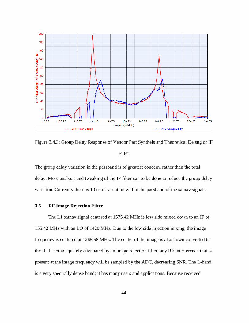
44
Figure 3.4.3: Group Delay Response of Vendor Part Syntheis and Theoretical Deisng of IF
Filter
The group delay variation in the passband is of greatest concern, rather than the total
delay. More analysis and tweaking of the IF filter can to be done to reduce the group delay
variation. Currently there is 10 ns of variation within the passband of the satnav signals.
3.5 RF Image Rejection Filter
The L1 satnav signal centered at 1575.42 MHz is low side mixed down to an IF of
155.42 MHz with an LO of 1420 MHz. Due to the low side injection mixing, the image
frequency is centered at 1265.58 MHz. The center of the image is also down converted to
the IF. If not adequately attenuated by an image rejection filter, any RF interference that is
present at the image frequency will be sampled by the ADC, decreasing SNR. The L-band
is a very spectrally dense band; it has many users and applications. Because received
45
satnav signals are below the thermal noise floor, RF inference present at the image
frequency that is not attenuated will degrade the SNR. Therefore, the RF image rejection
filters must attenuate interference at the image frequency to prevent it being sampled by
the ADC.
The RF image rejection filter must also attenuate adjacent channel interference that
is present. Signals that are not directly present in the L1 satnav band, but have a large
signal power, may saturate components in the signal path if not filtered.
The ceramic cavity resonators have a higher dielectric constant than air, allowing
for smaller cavity resonators than air filled. Cavity filters are ideal because of their small
size, ease of manufacturability, and ability to be surface mounted on a PCB.
Lorch Microwave, now Smith’s Interconnect, manufactures custom ceramic cavity
filters to meet the designers need. Group delay variations need to be minimized in the pass
band. The filter also needs over 70 dB of attenuation at the image frequency. The 70 dB of
attenuation ensures that when the ADC has full scale input power, there is zero energy
from the image frequency being digitized. The designer has ability to specify the number
of resonator sections, the resonator size, center frequency and the 3 dB bandwidth. For L1
satnav signals, the front-end needs 50 MHz of 3dB bandwidth and a center frequency of
1575.42 MHz. Increasing the number of resonator sections increases the group delay
variations while improving role off. Filters of 5, 4, and 2 resonators were simulated in
Genesys. Image rejection and group delay were assessed. Smaller resonator sizes are
preferred for the PCB layout.
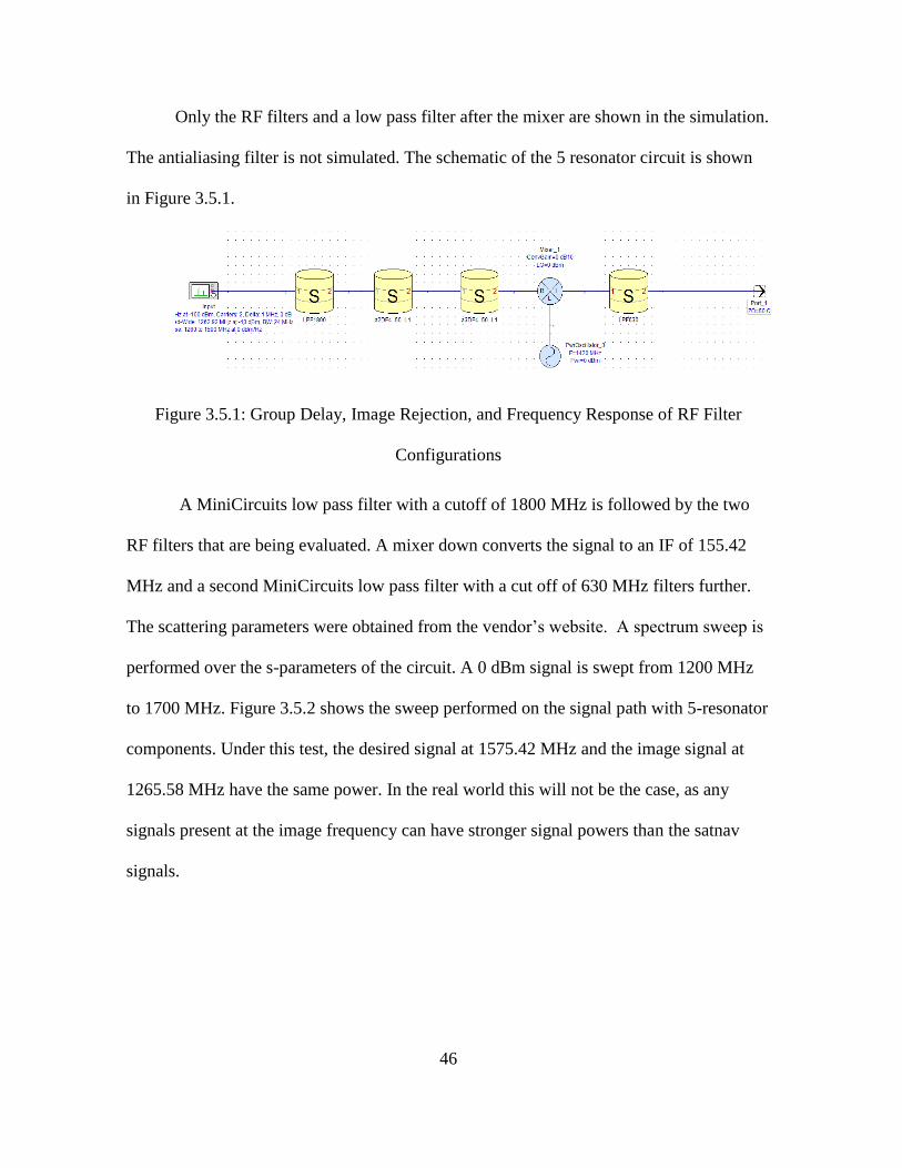
46
Only the RF filters and a low pass filter after the mixer are shown in the simulation.
The antialiasing filter is not simulated. The schematic of the 5 resonator circuit is shown
in Figure 3.5.1.
Figure 3.5.1: Group Delay, Image Rejection, and Frequency Response of RF Filter
Configurations
A MiniCircuits low pass filter with a cutoff of 1800 MHz is followed by the two
RF filters that are being evaluated. A mixer down converts the signal to an IF of 155.42
MHz and a second MiniCircuits low pass filter with a cut off of 630 MHz filters further.
The scattering parameters were obtained from the vendor’s website. A spectrum sweep is
performed over the s-parameters of the circuit. A 0 dBm signal is swept from 1200 MHz
to 1700 MHz. Figure 3.5.2 shows the sweep performed on the signal path with 5-resonator
components. Under this test, the desired signal at 1575.42 MHz and the image signal at
1265.58 MHz have the same power. In the real world this will not be the case, as any
signals present at the image frequency can have stronger signal powers than the satnav
signals.
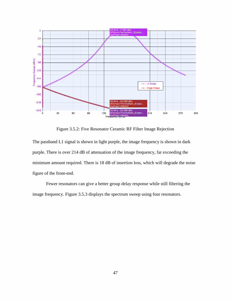
47
Figure 3.5.2: Five Resonator Ceramic RF Filter Image Rejection
The passband L1 signal is shown in light purple, the image frequency is shown in dark
purple. There is over 214 dB of attenuation of the image frequency, far exceeding the
minimum amount required. There is 18 dB of insertion loss, which will degrade the noise
figure of the front-end.
Fewer resonators can give a better group delay response while still filtering the
image frequency. Figure 3.5.3 displays the spectrum sweep using four resonators.
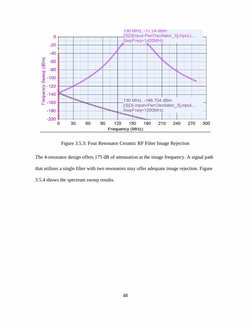
48
Figure 3.5.3: Four Resonator Ceramic RF Filter Image Rejection
The 4-resonator design offers 175 dB of attenuation at the image frequency. A signal path
that utilizes a single filter with two resonators may offer adequate image rejection. Figure
3.5.4 shows the spectrum sweep results.
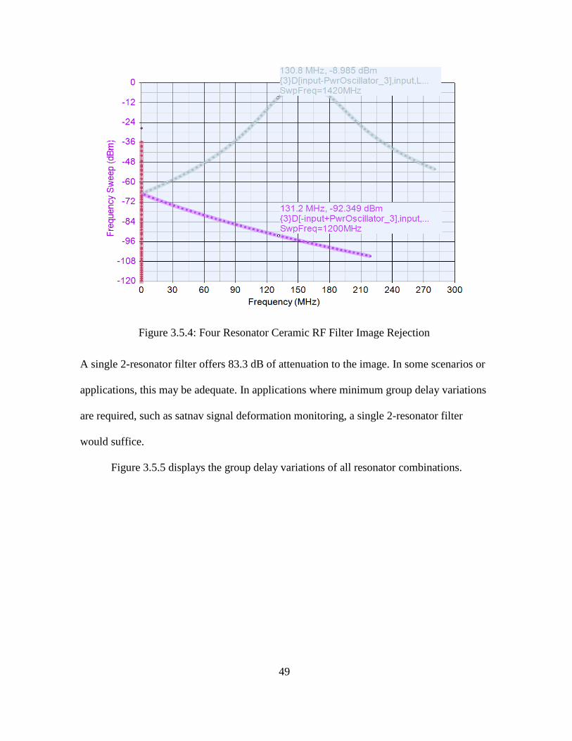
49
Figure 3.5.4: Four Resonator Ceramic RF Filter Image Rejection
A single 2-resonator filter offers 83.3 dB of attenuation to the image. In some scenarios or
applications, this may be adequate. In applications where minimum group delay variations
are required, such as satnav signal deformation monitoring, a single 2-resonator filter
would suffice.
Figure 3.5.5 displays the group delay variations of all resonator combinations.

50
Figure 3.5.5: Group Delay of RF Bandpass Filters
The large group delay variations within the passband is undesirable. A flat group delay
response in the center of the passband will add minimal signal deformations to the satnav
signal. Large group delay variations at the edges of the filters are unavoidable in resonator
filters. There is a minimum of 21.8 ns of delay at the center of the passband. If we desired
32 MHz of bandwidth for signal processing, the group delay variations will be 4 ns. The
group delay variations are sparse for the single 2-resonator filter. Depending upon the
amount of bandwidth needed for signal processing, the maximum group delay variations
will be approximately 2 ns for larger bandwidths. In building the layout for the front-end
the operator has the ability to choose to either use the two 2-resonator filters or one by
flipping capacitors on the PCB.
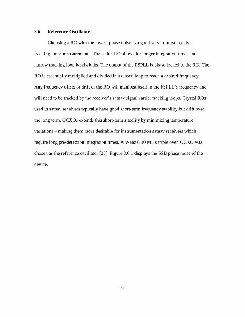
51
3.6 Reference Oscillator
Choosing a RO with the lowest phase noise is a good way improve receiver
tracking loops measurements. The stable RO allows for longer integration times and
narrow tracking loop bandwidths. The output of the FSPLL is phase locked to the RO. The
RO is essentially multiplied and divided in a closed loop to reach a desired frequency.
Any frequency offset or drift of the RO will manifest itself in the FSPLL’s frequency and
will need to be tracked by the receiver’s satnav signal carrier tracking loops. Crystal ROs
used in satnav receivers typically have good short-term frequency stability but drift over
the long term. OCXOs extends this short-term stability by minimizing temperature
variations – making them more desirable for instrumentation satnav receivers which
require long pre-detection integration times. A Wenzel 10 MHz triple oven OCXO was
chosen as the reference oscillator [25]. Figure 3.6.1 displays the SSB phase noise of the
device.
52
Figure 3.6.1: 10 MHz OCXO Reference Oscillator SSB Phase Noise
By multiplying the RO frequency of 10 MHz by 142, we are increasing the phase noise in
Figure 3.6.1 by 10 log10 142, or by 21.5 dB. Thus, the phase noise at M1 will be -144.4 +
21.5=-122.9 dBc at 1420 MHz.
3.7 Frequency Synthesizer Phase Locked Loop
The FSPLL is responsible for synthesizing the LO frequency using the RO as the
reference. Any phase noise on the FSPLL’s LO will be added to the phase of all received
satnav signals.
Spurs are considered to be 1-Hz bandwidth, and do not contribute much to the
overall integrated phase noise. The degradation caused by the spurs in the receiver’s
tracking loops are difficult to quantify. The spurs can mix in out-of-band signals into the
53
IF passband, decreasing the SNR [12], [26]. Integer boundary spurs will occur at offsets at
multiples of the PFD frequency [12]. This is due to the harmonics of the harmonics of the
PFD and charge pumps. Spurs can be created through voltage supply pins by injecting
spurious energy onto the ground and power rails causing crosstalk with the VCO and
charge pump [12].
The FSPLL’s lock time is of little concern in the given frequency plan, as only one LO
frequency is required for a given RF front-end.
There are several major contributing features of a FSPLL that impact the phase noise
and spur performance. The following attributes were derived for reducing phase noise and
spurs for FSPLL’s with integrated VCOs, charge pump, and PFD. The loop filter is the
only external component. Several of industry’s FSPLLs were configured and evaluated for
their performance in a high-fidelity satnav receiver, their results are in Section 4.4.
3.7.1 Integer-N Feedback Divider and the PFD Operation Frequency
For best spur and phase noise performance, the PLL should be operated in Integer-N
mode with a high PFD frequency. This limits the frequency step size of the FSPLL to
integer divisions of the RO. This may be a problem in frequency plans which require fine
frequency resolution of the LO. In which case Fractional-N may be more beneficial.
Fractional-N mode dithers between N and N+1 divide ratios to achieve fractional division
for finer frequency resolution on the output. However, the phase noise suffers, and spurs
are created closer to the LO. The spur locations are also difficult to predict and account for
in Fractional-N mode. Thus Integer-N division is preferred in FSPLLs for high-fidelity
54
satellite navigation and timing (satnav) receivers. Higher Integer-N divisions result in
increased phase noise by 20 log10𝑁
𝑀 , M being the input divider [12].
3.7.2 The RO input divider/multiplier M
Avoid using the RO divider if possible because it is best to operate the PFD at a higher
frequency, resulting in a lower N value. The ADF 4355-2, MAX 2871, and the LMX 2582
all have the option of a low noise reference frequency doubler. This is useful for lowering
the Integer-N divider but can increase spur power.
3.7.3 Loop Filter’s Bandwidth, Phase Margin, Order, and Pole Ratio
The loop filter, 𝐻𝐿𝐹(𝑠), is the most important component for determining phase noise,
stability, and spurs of the FSPLL. The loop filter is designed for a fixed value of N, 𝐼𝑝, and
𝐾𝑉𝐶𝑂. The bandwidth of the loop filter should be significantly smaller than the Nyquist
criteria set by the PFD frequency. For best integrated phase noise performance, the FSPLL
loop bandwidth is set to where the VCO phase noise intersects the PFD’s [12], [26]. The
phase margin controls the stability, lock time, and peaking of the phase noise filter shape.
High phase margins are desired because lock time is of little concern, greatly reduces
integrated phase noise, and increases loop stability. Higher-order filters may be desirable
for filtering spurs and improving lock time. If spurs are well outside the bandwidth of the
loop filter, second order filters will work best.
3.7.4 The Loop Gain
The loop gain is determined by the charge pump gain 𝐼𝑝 and the VCO sensitivity
𝐾𝑉𝐶𝑂. The designer has little control over the VCO sensitivity and is usually retrieved
55
from the devices’ data sheet or software tool provided by the manufacturer. The designer
can control the charge pump gain, 𝐼𝑝. For best phase noise performance, a high 𝐼𝑝 works
best. However larger 𝐼𝑝 results in larger loop filter passive components and spur power.
The loop gain is given by [12]:
𝐾 =𝐼𝑝𝐾𝑉𝐶𝑂
𝑁. (49)
The user can best improve phase noise between 0 Hz and 100 Hz by selecting a stable
RO. The VCO performance is manufacture specific. Wideband FSPLL are equipped with
multiple VCOs that are tuned to specific frequency ranges through switching capacitors
internal to the device. It is best to let the device pick and calibrate its VCO based on the
user defined frequency. The calibration is done during its initial pull in. The calibration
time does not matter in our design case as the LO is a single predefined frequency.
3.7.5 PCB Layout and Power
The traces on the external loop filter should not be exposed to electromagnetic
interference (EMI) from any RF, power, or digital signals present on the board. Any noise,
or EMI on the loop filter will manifest itself as phase noise in the VCO output. Low ripple
power supplies are essential for reducing spurious emissions. Ferrite beads should be used
on the VCO, charge pump, and digital power supply lines of the device in order to
minimize coupling. Grounded co-planar waveguide (GCPWG) RF traces should be used
for the RO and LO out traces for maximum isolation. RF coupling onto the LO should be
minimized. Class 1 temperature coefficient capacitors should be used in the loop filter,

56
such as capacitors with C0G dielectric material. With large loop gains, it may be a
challenge finding large C0G capacitors [12], [26].
3.8 Gain Control and Linearity for the ADC
The received signal power of the GPS L1C is -127 dBm given an isotropic antenna.
In a 50 MHz bandwidth receiver, the thermal noise power is -127 dBW, given through:
𝜎𝑁02 = 𝑘𝐵𝑇0𝐵 = (1.28 × 10²³)(295)(50 × 106) = 1.88 × 10⁻¹³ (𝑊), (50)
10 × log10 1.88 × 10−13 = −127 𝑑𝐵𝑊 = −97𝑑𝐵𝑚. (51)
The GPS L1C code is 30 dB below the thermal noise power in a 50 MHz receiver. The
goal of the receiver front-end is to amplify the noise floor, so it may be quantized by the
ADC. Interference or jamming is considered to be broadband over the 50 MHz passband.
If the receiver were to experience a 100 dB J/S environment, the thermal noise power will
equivocally be -57 dBW or -27 dBm of power. The maximum power the front-end is
designed for is -27 dBm. The front-end must amplify an input signal between -97 to -27
dBm to be quantized by the ADC. The AD9681 largest available input span is 2V peak-to-
peak. Over a 50 Ω load this equates to a maximum signal power of 10 dBm. With an
ENOB of 12, the ADC can quantize signals down to -62 dBm.
In the baseband signal processing of satnav signals, the correlators do not benefit
much from having a large sample bit depth [5]. Having large bit depths can prove a
hinderance in the correlation process due to computational resources required. With little
or no interference present, 1, 2 or 3 bits of quantization will suffice. Therefore, the
minimum amount of amplification needed is shown in Figure 3.8.1.

57
Figure 3.8.1: ADC Operation at -97 dBm Input Power
One added benefit of not amplifying the thermal noise power up the full scale of the ADC
is that a receiver can quantize and analyze any interference that may present itself. When
interference is present, there is 54 dB of dynamic range before attenuation is needed to
keep the ADC operating within its range. Figure 3.8.2 shows the ADC operating at full
scale.
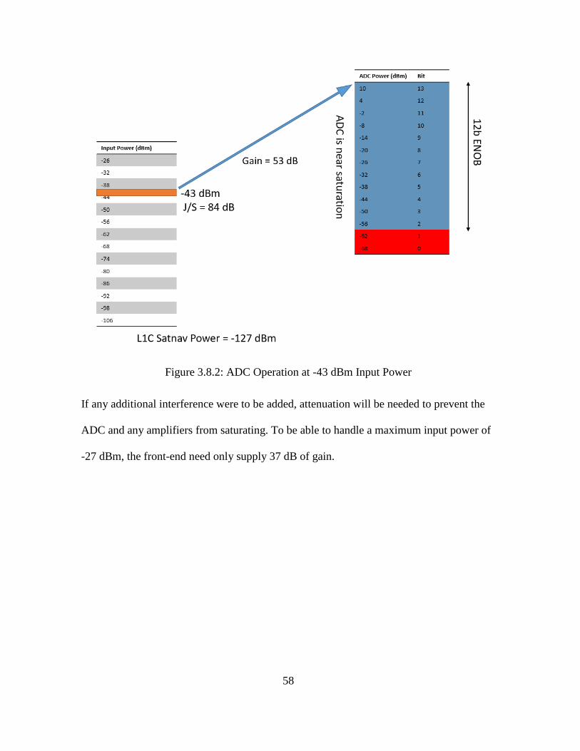
58
Figure 3.8.2: ADC Operation at -43 dBm Input Power
If any additional interference were to be added, attenuation will be needed to prevent the
ADC and any amplifiers from saturating. To be able to handle a maximum input power of
-27 dBm, the front-end need only supply 37 dB of gain.

59
Figure 3.8.3: ADC Operation at Full Scale Input Power (-27 dBm)
Employing an automatic gain control (AGC) to adjust the level of amplification based
upon on the number of bits being excited would work effectively in most satnav receivers.
However, an instrumentation satnav receiver should be able to sense the amount of
interference in the environment and be able to make accurate power interpretations of the
amount of interference received. An AGC can dilute the precision of a power reading.
Therefore, the receiver should be able to provide more than 53 dB of gain, and any
additional gain control will be set by adjusting the attenuation of some variable digital
attenuators (VDA). The VDA are also responsible for preventing the saturation of
amplifiers in the signal path. The HMC542B [27] is an ideal candidate, the device offers
0.5 dB steps of attenuation all the way up to 31.5 dB. The device also has a frequency
range of operation from DC to 4 GHz.

60
3.9 RMS Power Detector
An RMS power detector is useful for measuring the received signal power
regardless of the modulation type. The received signal power is expected to be between -
97 dBm and -27 dBm. The ADC can effectively quantize RF input signals up to -43 dBm
before the attenuators need to be adjusted. The RMS power detector can provide greater
insight into the true power received and can aid in adjusting the attenuation of the VDAs.
The HMC1020 [28] has a 1 dB detection accuracy from DC to 3.9 GHz and an input
dynamic range from -65 dBm to +7 dBm making it an ideal candidate for sensing the RF
input power after the ADC is close to saturation. Figure 3.9.1 shows the position of the
HMC1020 in the signal path.
Figure 3.9.1: RMS Power Detector Signal Path
At minimum, the RMS power detector will receive -84 dBm, accounting for the losses in
the power splitters and filters, well below its dynamic range. When the received signal
power at the antenna is -43 dBm, the RMS power detector will receive -31 dBm, well
within its dynamic range, and with the ability to sense an additional 38 dB of dynamic
range. The HMC 1020 can effectively make power measurements well over the 100 dB
J/S threshold the front-end is designed to handle.

61
3.10 Gain Control, Noise Figure and Linearity RF Calculator
The noise figure of the front-end is the amount of degradation of the SNR
contributed by the antenna’s temperature, transmission line loss, and LNAs. Transmission
line length from the antenna to the first LNA should be minimized to keep a low noise
figure. Depending on the cable quality, losses can incur from 25 dB/100ft to 1.3 dB/100ft.
Antennas with integrated LNAs greatly improve the noise figure. Selecting the first couple
amplifiers in the signal path sets the noise figure of the front-end. They need to be able to
handle the -29 dBm input power while keeping linearity. The first two amplifiers in the
signal chain were chosen to be the MAAL-010704 [29] and the TQP3M9005 [30]
respectively. Cascaded, they contribute 26 dB of gain, and have a noise figure of 0.83 dB.
The fastest and simplest way to assess the performance of the signal path under
certain RF input conditions is to build a spread sheet calculator that computes the RF
power, noise figure, and linearity after each device in the signal path. By this method, one
can see when amplifiers are operating near their saturation regions and configure the
attenuators to preserve linearity. The voltage and current consumed by each device is also
included. By knowing the power consumption of the front-end an appropriate voltage
regulator can be selected. Table 3.10.1 shows the signal path under nominal conditions.
The received signal power from a passive antenna is -97 dBm.
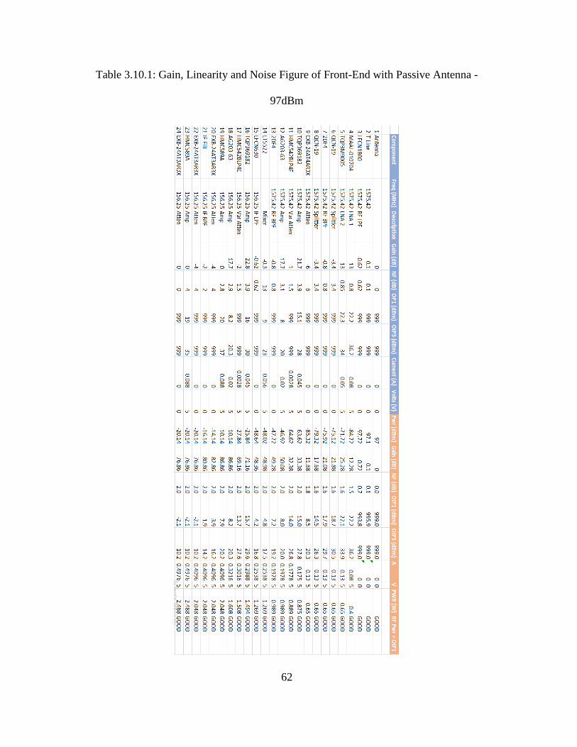
62
Table 3.10.1: Gain, Linearity and Noise Figure of Front-End with Passive Antenna -
97dBm
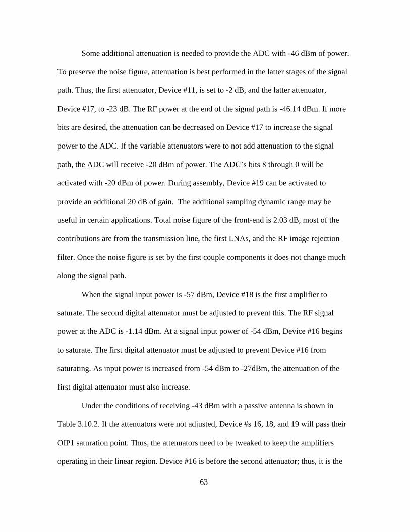
63
Some additional attenuation is needed to provide the ADC with -46 dBm of power.
To preserve the noise figure, attenuation is best performed in the latter stages of the signal
path. Thus, the first attenuator, Device #11, is set to -2 dB, and the latter attenuator,
Device #17, to -23 dB. The RF power at the end of the signal path is -46.14 dBm. If more
bits are desired, the attenuation can be decreased on Device #17 to increase the signal
power to the ADC. If the variable attenuators were to not add attenuation to the signal
path, the ADC will receive -20 dBm of power. The ADC’s bits 8 through 0 will be
activated with -20 dBm of power. During assembly, Device #19 can be activated to
provide an additional 20 dB of gain. The additional sampling dynamic range may be
useful in certain applications. Total noise figure of the front-end is 2.03 dB, most of the
contributions are from the transmission line, the first LNAs, and the RF image rejection
filter. Once the noise figure is set by the first couple components it does not change much
along the signal path.
When the signal input power is -57 dBm, Device #18 is the first amplifier to
saturate. The second digital attenuator must be adjusted to prevent this. The RF signal
power at the ADC is -1.14 dBm. At a signal input power of -54 dBm, Device #16 begins
to saturate. The first digital attenuator must be adjusted to prevent Device #16 from
saturating. As input power is increased from -54 dBm to -27dBm, the attenuation of the
first digital attenuator must also increase.
Under the conditions of receiving -43 dBm with a passive antenna is shown in
Table 3.10.2. If the attenuators were not adjusted, Device #s 16, 18, and 19 will pass their
OIP1 saturation point. Thus, the attenuators need to be tweaked to keep the amplifiers
operating in their linear region. Device #16 is before the second attenuator; thus, it is the

64
first attenuator’s responsibility to keep Device #16 in the linear region. The second
attenuator will keep Device #s 18 and 19 linear.
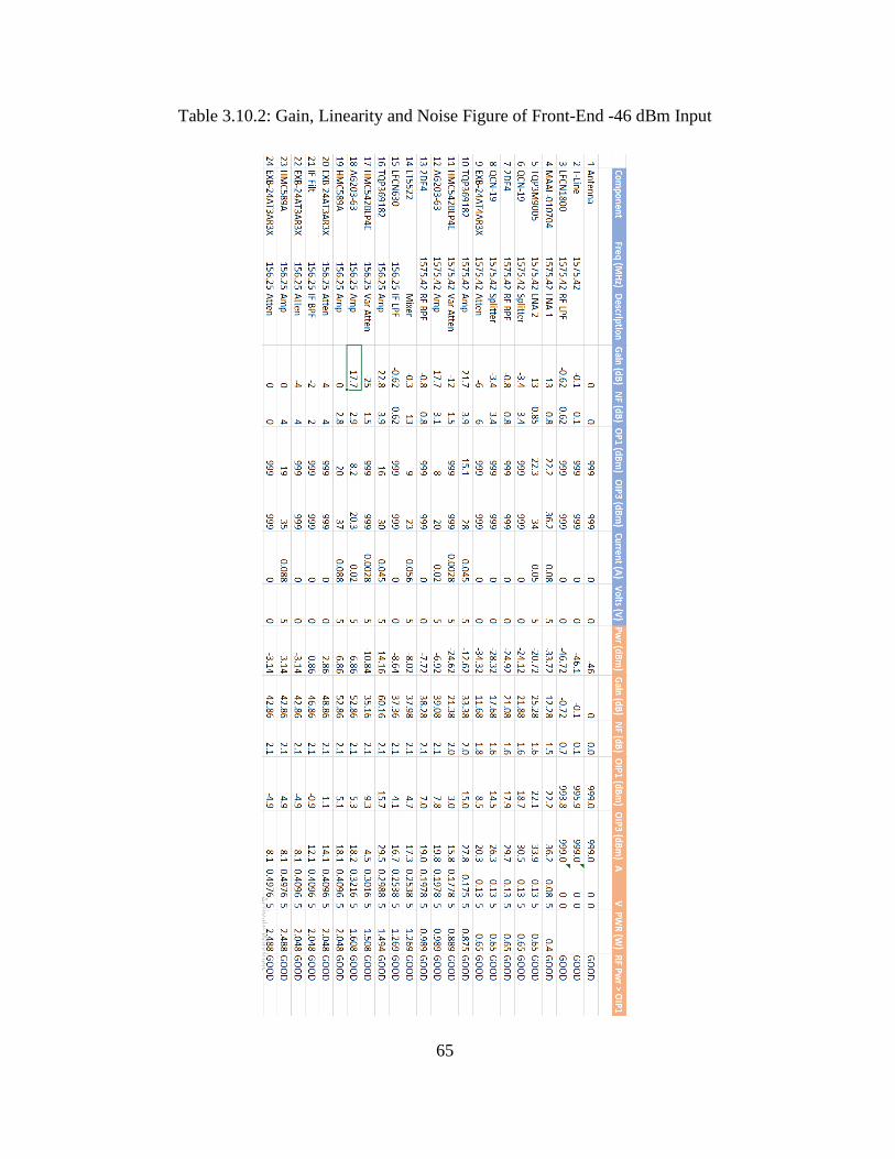
65
Table 3.10.2: Gain, Linearity and Noise Figure of Front-End -46 dBm Input

66
The ADC will receive -3.14 dBm of power, due to the losses incurred from the IF
filter and the 4 dB attenuators on either side of the filter that are used for improving
matching. The noise figure here is slightly worse at 2.08 dB, of course this due to the
additional attenuation needed in the RF portion of the signal chain.
The maximum designed power the front can receive is -27 dBm with a passive
antenna. The received signal power of an L1C signal is now 100 dB below the
interference power. Table 3.10.3 shows the total signal gain and noise figure of the signal
path.
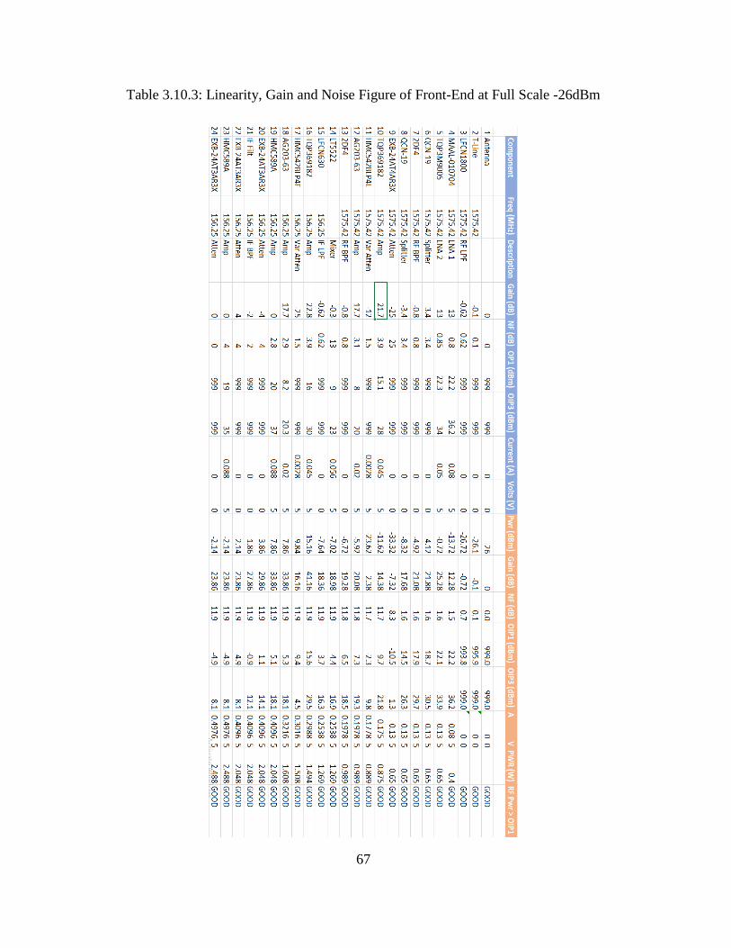
67
Table 3.10.3: Linearity, Gain and Noise Figure of Front-End at Full Scale -26dBm

68
3.11 Nonlinear Simulation of Front-End
Keysight Genesys 2018 offers an alternative method for simulating the signal
chain. Component vendors typically offer Touchstone files to designers [31]. The
Touchtone files ‘.s2p’ provide the scattering parameters of the device which can be used
in linear simulations. A linear simulation is helpful for understanding the gain and phase
relationships in the design. The component vendors also provide OIP3, OIP1, and
OIPSAT points which clarify the nonlinearities of the devices. Genesys can provide linear
and nonlinear simulations of the devices to gain a better insight into the behavior of the
signal chain. Figure 3.11.1 shows the signal path of Genesys simulations. All passive
components are modeled with the s-parameters. All active components are modeled with
their OIP3, OIP1, and OIPSAT. The IF filter that was designed with VPS is inserted into
the design as well as the two 2-resonator RF image rejection filters. The same signal path
that was used in the simple RF calculator is used here.
Figure 3.11.1: Genesys Nonlinear Signal Path Simulation
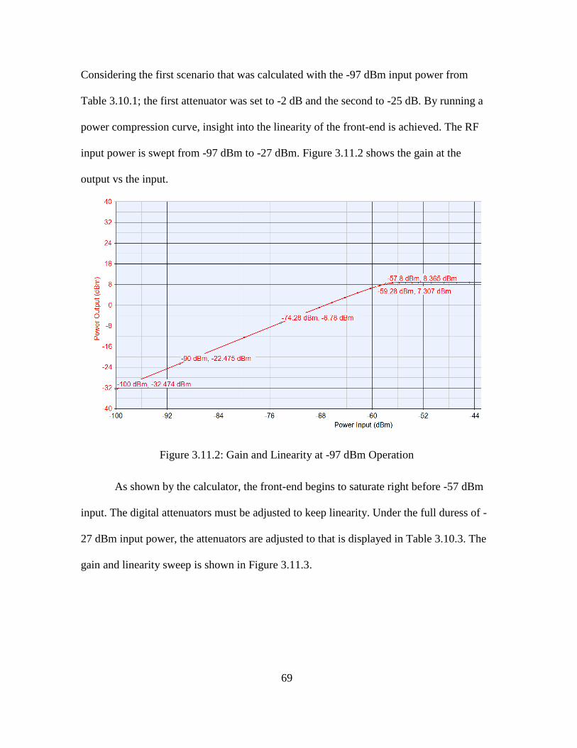
69
Considering the first scenario that was calculated with the -97 dBm input power from
Table 3.10.1; the first attenuator was set to -2 dB and the second to -25 dB. By running a
power compression curve, insight into the linearity of the front-end is achieved. The RF
input power is swept from -97 dBm to -27 dBm. Figure 3.11.2 shows the gain at the
output vs the input.
Figure 3.11.2: Gain and Linearity at -97 dBm Operation
As shown by the calculator, the front-end begins to saturate right before -57 dBm
input. The digital attenuators must be adjusted to keep linearity. Under the full duress of -
27 dBm input power, the attenuators are adjusted to that is displayed in Table 3.10.3. The
gain and linearity sweep is shown in Figure 3.11.3.
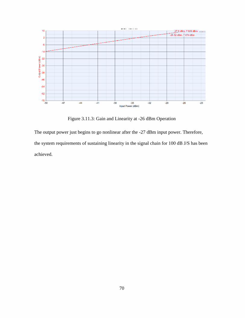
70
Figure 3.11.3: Gain and Linearity at -26 dBm Operation
The output power just begins to go nonlinear after the -27 dBm input power. Therefore,
the system requirements of sustaining linearity in the signal chain for 100 dB J/S has been
achieved.
71
IV. Analysis and Results
4.1 Introduction
This chapter attempts to validate the design methodologies and show performance
of the front-end. Specialized RF components were evaluated and constructed for a high-
fidelity satnav receiver.
Waveguides were constructed and evaluated on a chosen PCB stack-up. Insertion
loss and reflections were evaluated over the satnav frequencies of operation. The first
LNA in the antenna electronics or the front-end is essential for determining the noise
figure and sensitivity. Careful evaluation of a high performing LNA was evaluated for its
linearity, gain, and power consumption. The LO in the frequency plan is essential for
determining the sensitivity of carrier phase measurements. Careful evaluation of several
industry leading FSPLLs with integrated charge pumps and VCOs was conducted for use
in a satnav receiver.
The front-end was then assembled and portions tested for performance. Simulated
and live-sky signals were then injected into the front-end. Data was sampled, recorded and
evaluated in a software defined receiver. The font-end’s LO was compared against a
proven FSPLL that has been used in satnav instrumentation receivers. The front-end’s
tracking performance was also compared against an industry leading manufacture of
satnav reference receivers.
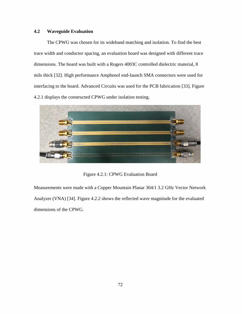
72
4.2 Waveguide Evaluation
The CPWG was chosen for its wideband matching and isolation. To find the best
trace width and conductor spacing, an evaluation board was designed with different trace
dimensions. The board was built with a Rogers 4003C controlled dielectric material, 8
mils thick [32]. High performance Amphenol end-launch SMA connectors were used for
interfacing to the board. Advanced Circuits was used for the PCB fabrication [33]. Figure
4.2.1 displays the constructed CPWG under isolation testing.
Figure 4.2.1: CPWG Evaluation Board
Measurements were made with a Copper Mountain Planar 304/1 3.2 GHz Vector Network
Analyzer (VNA) [34]. Figure 4.2.2 shows the reflected wave magnitude for the evaluated
dimensions of the CPWG.
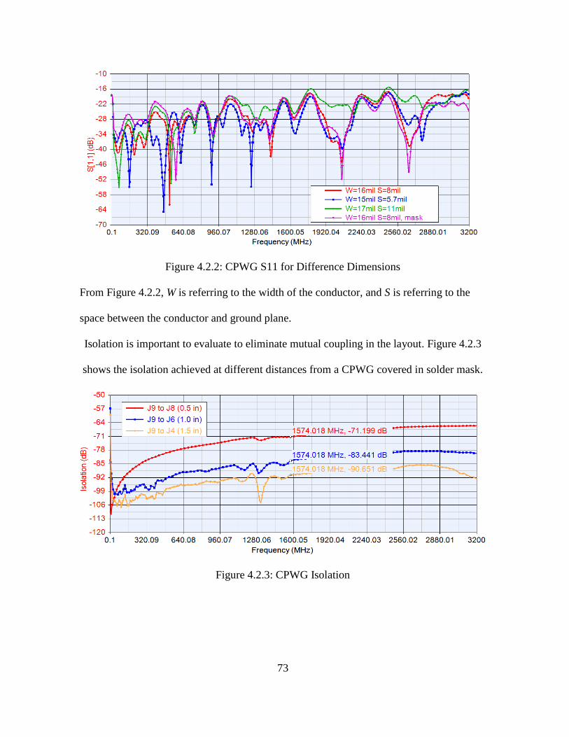
73
Figure 4.2.2: CPWG S11 for Difference Dimensions
From Figure 4.2.2, W is referring to the width of the conductor, and S is referring to the
space between the conductor and ground plane.
Isolation is important to evaluate to eliminate mutual coupling in the layout. Figure 4.2.3
shows the isolation achieved at different distances from a CPWG covered in solder mask.
Figure 4.2.3: CPWG Isolation
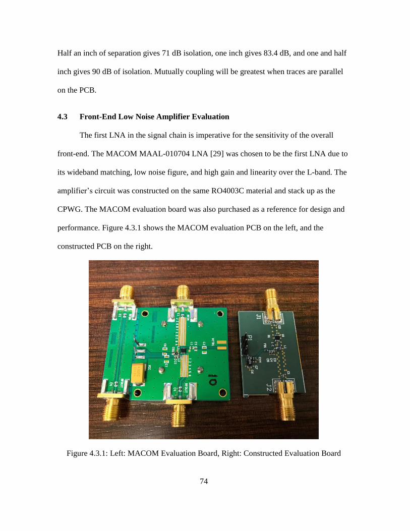
74
Half an inch of separation gives 71 dB isolation, one inch gives 83.4 dB, and one and half
inch gives 90 dB of isolation. Mutually coupling will be greatest when traces are parallel
on the PCB.
4.3 Front-End Low Noise Amplifier Evaluation
The first LNA in the signal chain is imperative for the sensitivity of the overall
front-end. The MACOM MAAL-010704 LNA [29] was chosen to be the first LNA due to
its wideband matching, low noise figure, and high gain and linearity over the L-band. The
amplifier’s circuit was constructed on the same RO4003C material and stack up as the
CPWG. The MACOM evaluation board was also purchased as a reference for design and
performance. Figure 4.3.1 shows the MACOM evaluation PCB on the left, and the
constructed PCB on the right.
Figure 4.3.1: Left: MACOM Evaluation Board, Right: Constructed Evaluation Board

75
The designer has the ability to apply a voltage bias to a pin on the LNA that controls the
gain and power consumption of the board. Gain and linearity is favorable, if the max
current draw isn’t being exceeded. Different resistors were evaluated for their
performance. The Planar 403/1 VNA was used for collecting measurement data. Figure
4.3.2 shows gain of the device as a function of input power. The device begins to saturate
as the gain begins to tail off under higher input power.
Figure 4.3.2: MAL-010704 LNA Gain and Linearity vs. Bias
The current consumption under each test was recorded in Table 4.3.1. This aids in
calculating the power consumption of the entire front-end.

76
Table 4.3.1: MAL-010704 LNA Current Consumption
Bias Resistor (Ω) Current Consumption (mA)
309 81
392 72
442 67
549 59
1000 38
Matching of the amplifier is shown Figure 4.3.3. The amplifier is well matched over the
span of the L-band. This eliminates the need for requiring external matching components
that contribute their own losses to the signal.
Figure 4.3.3: S11 of MAL-010704 LNA
The 309 Ω bias resistor was chosen for operation due to its higher gain and linearity over
the other bias resistors.
4.4 Frequency Synthesizer Evaluation
Several PLLs with integrated charge-pumps and VCOs were evaluated for their
performance as a LO in the frequency plan. A single-ended 10 MHz triple OCXO is used
to supply the RO to all device evaluation boards. Some boards contained their own linear
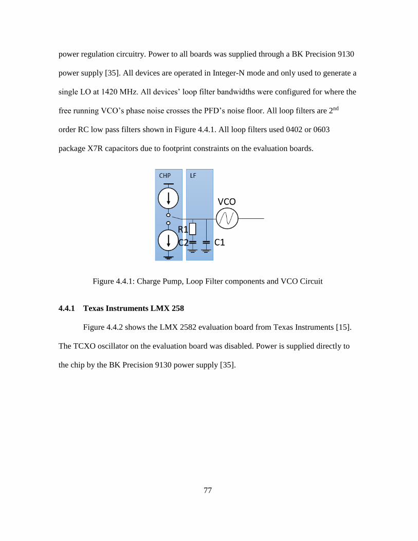
77
power regulation circuitry. Power to all boards was supplied through a BK Precision 9130
power supply [35]. All devices are operated in Integer-N mode and only used to generate a
single LO at 1420 MHz. All devices’ loop filter bandwidths were configured for where the
free running VCO’s phase noise crosses the PFD’s noise floor. All loop filters are 2nd
order RC low pass filters shown in Figure 4.4.1. All loop filters used 0402 or 0603
package X7R capacitors due to footprint constraints on the evaluation boards.
Figure 4.4.1: Charge Pump, Loop Filter components and VCO Circuit
4.4.1 Texas Instruments LMX 258
Figure 4.4.2 shows the LMX 2582 evaluation board from Texas Instruments [15].
The TCXO oscillator on the evaluation board was disabled. Power is supplied directly to
the chip by the BK Precision 9130 power supply [35].
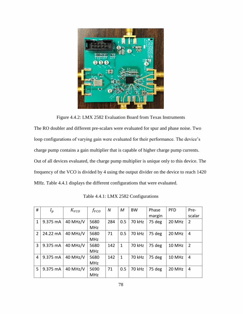
78
Figure 4.4.2: LMX 2582 Evaluation Board from Texas Instruments
The RO doubler and different pre-scalars were evaluated for spur and phase noise. Two
loop configurations of varying gain were evaluated for their performance. The device’s
charge pump contains a gain multiplier that is capable of higher charge pump currents.
Out of all devices evaluated, the charge pump multiplier is unique only to this device. The
frequency of the VCO is divided by 4 using the output divider on the device to reach 1420
MHz. Table 4.4.1 displays the different configurations that were evaluated.
Table 4.4.1: LMX 2582 Configurations
# 𝐼𝑝 𝐾𝑉𝐶𝑂 𝑓𝑉𝐶𝑂 N M BW Phase margin
PFD Pre-scalar
1 9.375 mA 40 MHz/V 5680 MHz
284 0.5 70 kHz 75 deg 20 MHz 2
2 24.22 mA 40 MHz/V 5680 MHz
71 0.5 70 kHz 75 deg 20 MHz 4
3 9.375 mA 40 MHz/V 5680 MHz
142 1 70 kHz 75 deg 10 MHz 2
4 9.375 mA 40 MHz/V 5680 MHz
142 1 70 kHz 75 deg 10 MHz 4
5 9.375 mA 40 MHz/V 5690 MHz
71 0.5 70 kHz 75 deg 20 MHz 4
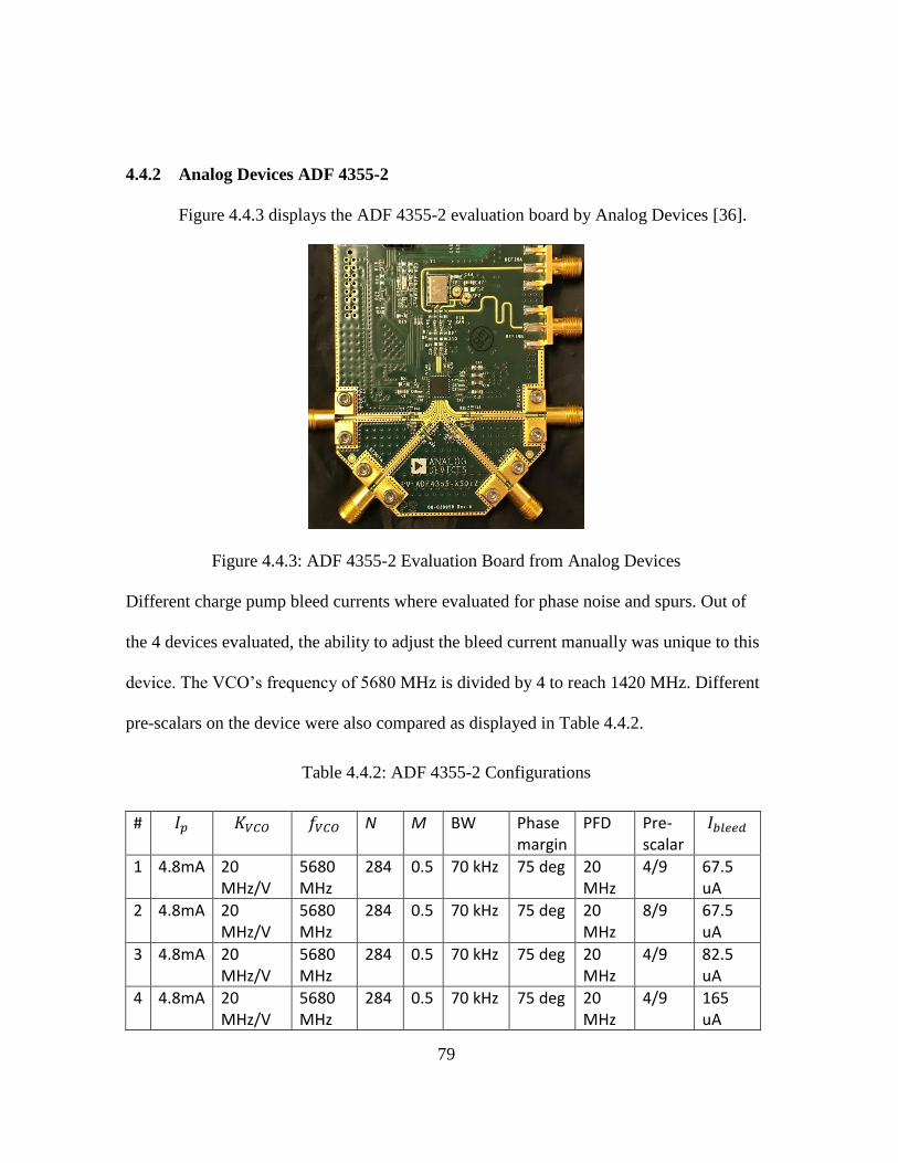
79
4.4.2 Analog Devices ADF 4355-2
Figure 4.4.3 displays the ADF 4355-2 evaluation board by Analog Devices [36].
Figure 4.4.3: ADF 4355-2 Evaluation Board from Analog Devices
Different charge pump bleed currents where evaluated for phase noise and spurs. Out of
the 4 devices evaluated, the ability to adjust the bleed current manually was unique to this
device. The VCO’s frequency of 5680 MHz is divided by 4 to reach 1420 MHz. Different
pre-scalars on the device were also compared as displayed in Table 4.4.2.
Table 4.4.2: ADF 4355-2 Configurations
# 𝐼𝑝 𝐾𝑉𝐶𝑂 𝑓𝑉𝐶𝑂 N M BW Phase margin
PFD Pre-scalar
𝐼𝑏𝑙𝑒𝑒𝑑
1 4.8mA 20 MHz/V
5680 MHz
284 0.5 70 kHz 75 deg 20 MHz
4/9 67.5 uA
2 4.8mA 20 MHz/V
5680 MHz
284 0.5 70 kHz 75 deg 20 MHz
8/9 67.5 uA
3 4.8mA 20 MHz/V
5680 MHz
284 0.5 70 kHz 75 deg 20 MHz
4/9 82.5 uA
4 4.8mA 20 MHz/V
5680 MHz
284 0.5 70 kHz 75 deg 20 MHz
4/9 165 uA
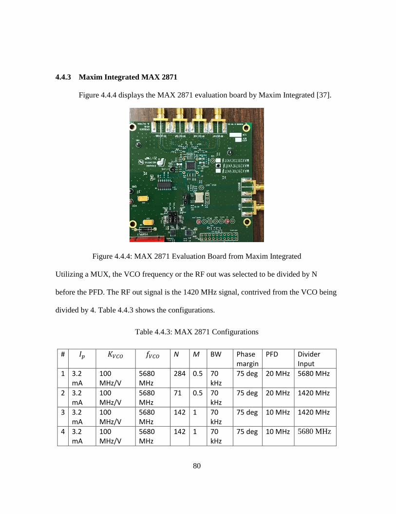
80
4.4.3 Maxim Integrated MAX 2871
Figure 4.4.4 displays the MAX 2871 evaluation board by Maxim Integrated [37].
Figure 4.4.4: MAX 2871 Evaluation Board from Maxim Integrated
Utilizing a MUX, the VCO frequency or the RF out was selected to be divided by N
before the PFD. The RF out signal is the 1420 MHz signal, contrived from the VCO being
divided by 4. Table 4.4.3 shows the configurations.
Table 4.4.3: MAX 2871 Configurations
# 𝐼𝑝 𝐾𝑉𝐶𝑂 𝑓𝑉𝐶𝑂 N M BW Phase margin
PFD Divider Input
1 3.2 mA
100 MHz/V
5680 MHz
284 0.5 70 kHz
75 deg 20 MHz 5680 MHz
2 3.2 mA
100 MHz/V
5680 MHz
71 0.5 70 kHz
75 deg 20 MHz 1420 MHz
3 3.2 mA
100 MHz/V
5680 MHz
142 1 70 kHz
75 deg 10 MHz 1420 MHz
4 3.2 mA
100 MHz/V
5680 MHz
142 1 70 kHz
75 deg 10 MHz 5680 MHz
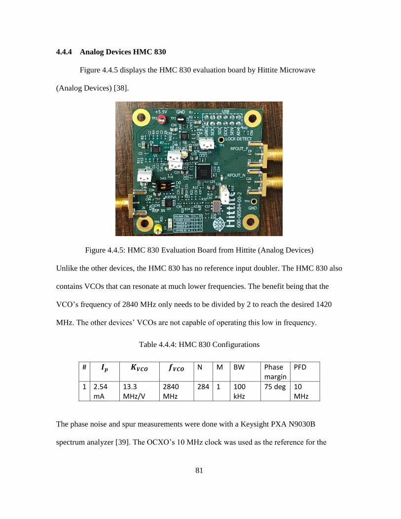
81
4.4.4 Analog Devices HMC 830
Figure 4.4.5 displays the HMC 830 evaluation board by Hittite Microwave
(Analog Devices) [38].
Figure 4.4.5: HMC 830 Evaluation Board from Hittite (Analog Devices)
Unlike the other devices, the HMC 830 has no reference input doubler. The HMC 830 also
contains VCOs that can resonate at much lower frequencies. The benefit being that the
VCO’s frequency of 2840 MHz only needs to be divided by 2 to reach the desired 1420
MHz. The other devices’ VCOs are not capable of operating this low in frequency.
Table 4.4.4: HMC 830 Configurations
# 𝑰𝒑 𝑲𝑽𝑪𝑶 𝒇𝑽𝑪𝑶 N M BW Phase margin
PFD
1 2.54 mA
13.3 MHz/V
2840 MHz
284 1 100 kHz
75 deg 10 MHz
The phase noise and spur measurements were done with a Keysight PXA N9030B
spectrum analyzer [39]. The OCXO’s 10 MHz clock was used as the reference for the
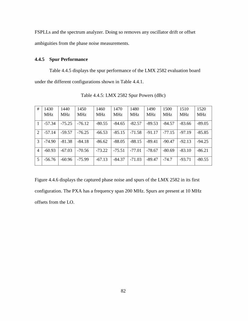
82
FSPLLs and the spectrum analyzer. Doing so removes any oscillator drift or offset
ambiguities from the phase noise measurements.
4.4.5 Spur Performance
Table 4.4.5 displays the spur performance of the LMX 2582 evaluation board
under the different configurations shown in Table 4.4.1.
Table 4.4.5: LMX 2582 Spur Powers (dBc)
# 1430
MHz
1440
MHz
1450
MHz
1460
MHz
1470
MHz
1480
MHz
1490
MHz
1500
MHz
1510
MHz
1520
MHz
1 -57.34 -75.25 -76.12 -80.55 -84.65 -82.57 -89.53 -84.57 -83.66 -89.05
2 -57.14 -59.57 -76.25 -66.53 -85.15 -71.58 -91.17 -77.15 -97.19 -85.85
3 -74.90 -81.38 -84.18 -86.62 -88.05 -88.15 -89.41 -90.47 -92.13 -94.25
4 -60.93 -67.03 -70.56 -73.22 -75.51 -77.01 -78.67 -80.69 -83.10 -86.21
5 -56.76 -60.96 -75.99 -67.13 -84.37 -71.03 -89.47 -74.7 -93.71 -80.55
Figure 4.4.6 displays the captured phase noise and spurs of the LMX 2582 in its first
configuration. The PXA has a frequency span 200 MHz. Spurs are present at 10 MHz
offsets from the LO.

83
Figure 4.4.6: LMX 2582 Spurs in Configuration # 1
Spurs for the ADF 4355-2 configurations are shown in Table 4.4.6.
Table 4.4.6: ADF 4355-2 Spur Powers (dBc)
# 1430 MHz
1440 MHz
1450 MHz
1460 MHz
1470 MHz
1480 MHz
1490 MHz
1500 MHz
1510 MHz
1520 MHz
1 -41.77 -64.61 -61.37 -63.37 -71.97 -62.53 -87.80 -61.53 -80.98 -64.75
2 -42.03 -64.72 -61.84 -64.5 -72.69 -62.85 -87.88 -61.76 -83.63 -65.09
3 -42.07 -63.73 -62.40 -69.02 -72.81 -64.98 -77.00 -63.53 -74.02 -65.48
4 -42.07 -63.71 -62.39 -69.00 -72.82 -64.97 -77.08 -63.53 -74.02 -65.49
Spurs for the MAX 2871 are shown in Table 4.4.7.

84
Table 4.4.7: MAX 2871 Spur Powers (dBc)
# 1430
MHz
1440
MHz
1450
MHz
1460
MHz
1470
MHz
1480
MHz
1490
MHz
1500
MHz
1510
MHz
1520
MHz
1 -42.58 -72.53 -61.99 -78.87 -71.76 -82.31 -79.03 -84.43 -84.42 -85.77
2 -45.75 -73.66 -64.02 -79.58 -73.07 -83.92 -79.88 -87.96 -85.35 -91.75
3 -90.37 -88.27 -92.89 -90.61 -90.67 -92.78 -89.68 -96.13 -88.82 -98.83
4 -93.23 -98.84 -102.04 -95.14 -103.14 -93.17 -97.94 -92.84 -99.14 -92.59
Spurs for the HMC 830 are shown in Table 4.4.8.
Table 4.4.8: HMC 830 Spur Powers (dBc)
# 1430
MHz
1440
MHz
1450
MHz
1460
MHz
1470
MHz
1480
MHz
1490
MHz
1500
MHz
1510
MHz
1520
MHz
1 -84.7 -92.99 -96.63 -98.72 -101.88 -103.18 -108.08 -105.08 -107.08 -105.38
Figure 4.4.1 displays the captured spurs of the HMC 830.
Figure 4.4.7: HMC 830 Spurs in Configuration # 1
85
The HMC 830 had the best spur performance for the given frequency plan. The frequency
doubler used to increase the frequency of the RO before the PFD was used in the LMX
2582, MAX 2871, and ADF 4355-2. While this helps to decrease N, the spur power was
increased by approximately 10 to 20 dB with the doubler enabled. The LMX 2582, MAX
2871, and ADF 4355-2 also need a VCO frequency of 5680 MHz, which is divided by 4 to
reach 1420 MHz. This output divider contributes its own spurious activity to the device.
4.4.6 Phase Noise Performance
Phase noise from each configuration is calculated from integrating the SSB PSD
from 10 Hz to 10 MHz and converting to RMS error in degrees by:
𝜎𝜙 =180
𝜋√[ ∫ P𝜙(𝑓)𝑑𝑓
10𝐸6
10
]. (52)
The PSD, P𝜙(𝑓), is normalized to the power of the carrier. The RMS phase error, 𝜎𝜙, is
the parameter error estimate of the receiver tracking loops. Figure 4.4.8 shows how the
phase noise data was gathered with the PXA N9030B [39]. 40 seconds of data were
collected with a complex sample rate of 10 MHz with the PXA. The collected data were
segmented into 40 blocks, each containing 1 second worth of data. A periodogram was
calculated with the 40 blocks forming a reasonable estimate of the devices’ phase noise
with 1-Hz resolution. An RF low pass filter was placed on the output of the FSPLL to
attenuate any odd-order harmonics that would otherwise be aliased by the PXA’s ADC.
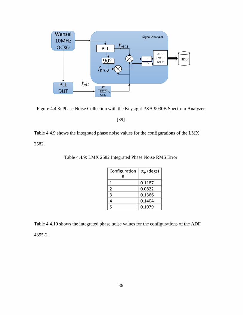
86
Figure 4.4.8: Phase Noise Collection with the Keysight PXA 9030B Spectrum Analyzer
[39]
Table 4.4.9 shows the integrated phase noise values for the configurations of the LMX
2582.
Table 4.4.9: LMX 2582 Integrated Phase Noise RMS Error
Configuration #
𝜎𝜙 (degs)
1 0.1187
2 0.0822
3 0.1366
4 0.1404
5 0.1079
Table 4.4.10 shows the integrated phase noise values for the configurations of the ADF
4355-2.
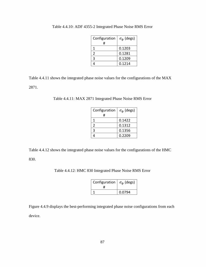
87
Table 4.4.10: ADF 4355-2 Integrated Phase Noise RMS Error
Configuration #
𝜎𝜙 (degs)
1 0.1203
2 0.1281
3 0.1209
4 0.1214
Table 4.4.11 shows the integrated phase noise values for the configurations of the MAX
2871.
Table 4.4.11: MAX 2871 Integrated Phase Noise RMS Error
Configuration #
𝜎𝜙 (degs)
1 0.1422
2 0.1312
3 0.1356
4 0.2209
Table 4.4.12 shows the integrated phase noise values for the configurations of the HMC
830.
Table 4.4.12: HMC 830 Integrated Phase Noise RMS Error
Configuration #
𝜎𝜙 (degs)
1 0.0794
Figure 4.4.9 displays the best-performing integrated phase noise configurations from each
device.
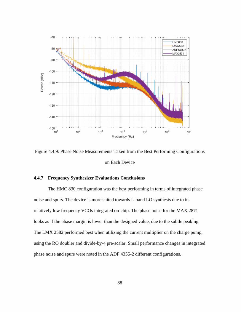
88
Figure 4.4.9: Phase Noise Measurements Taken from the Best Performing Configurations
on Each Device
4.4.7 Frequency Synthesizer Evaluations Conclusions
The HMC 830 configuration was the best performing in terms of integrated phase
noise and spurs. The device is more suited towards L-band LO synthesis due to its
relatively low frequency VCOs integrated on-chip. The phase noise for the MAX 2871
looks as if the phase margin is lower than the designed value, due to the subtle peaking.
The LMX 2582 performed best when utilizing the current multiplier on the charge pump,
using the RO doubler and divide-by-4 pre-scalar. Small performance changes in integrated
phase noise and spurs were noted in the ADF 4355-2 different configurations.
89
Changing the pre-scalar values or using the VCO output divider as feedback signal
to reduce N had little effect on the phase nose. The feedback division still remains 284 for
a VCO of 5680 MHz. Thus, the best way to reduce the feedback division is to increase the
RO frequency and decrease the VCO frequency.
In the end, the LMX 2582 was chosen as the frequency synthesizer of choice due
to the simple PCB layout and power requirements. While the HMC 830 did have better
spur and phase noise performance, the LMX 2582 was easier to design with and offered
similar phase noise performance.
4.5 Frequency Synthesizer Design
The PCB was built with the same stack up evaluated in the Section 4.2. Figure
4.5.1 displays the LMX 2582 soldered to the front-end. The various capacitors around the
device are used decoupling, energy storage, DC blocking and the loop filter.

90
Figure 4.5.1: Constructed LMX 2582 Circuit
The LMX 2582 and loop filter were configured as # 2 in Table 4.4.1. C0G temperature
coefficient capacitors were used in the loop filter design. Proper RF layout guidelines and
the manufacture’s recommended circuit design were followed. Ferrite beads were used on
all power supply inputs of the device to prevent leakage and coupling to other inputs. The
loop filter is routed on the bottom of the board, underneath the chip. Figure 4.5.2 displays
the captured phase noise spectra obtained from the same procedure in Section 4.4.
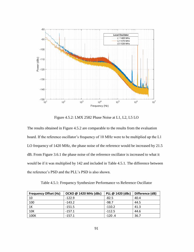
91
Figure 4.5.2: LMX 2582 Phase Noise at L1, L2, L5 LO
The results obtained in Figure 4.5.2 are comparable to the results from the evaluation
board. If the reference oscillator’s frequency of 10 MHz were to be multiplied up the L1
LO frequency of 1420 MHz, the phase noise of the reference would be increased by 21.5
dB. From Figure 3.6.1 the phase noise of the reference oscillator is increased to what it
would be if it was multiplied by 142 and included in Table 4.5.1. The difference between
the reference’s PSD and the PLL’s PSD is also shown.
Table 4.5.1: Frequency Synthesizer Performance vs Reference Oscillator
Frequency Offset (Hz) OCXO @ 1420 MHz (dBc) PLL @ 1420 (dBc) Difference (dB)
10 -122.9 -82.5 40.4
100 -143.2 -98.7 44.5
1K -151.5 -110.2 41.3
10K -157.1 -112.5 44.6
100K -157.1 -120 .4 36.7

92
4.6 Power Supply Design
A 6V supply is used to power the board. Linear regulators create the required
voltages for the board. Amplifiers, mixers, attenuators, and the RMS power detector run
off a 5.0 V supply rail generated by low drop out regulator ADP3339 [40]. The 5.0 V
supply is used by another RF linear regulator (ADM7150) [41] used to supply 3.3 V to
FSPLL LMX2582. Figure 4.6.1 displays the power supply section of the PCB. A small
heat sink was built to help dissipate heat created by the linear regulator.
Figure 4.6.1: Front-End Power Supply Linear Voltage Regulators
RMS power measurements were made with a Lecroy 760Zi Oscilloscope [42]. The power
signal is AC coupled when it sampled by the instrument. Figure 4.6.2 displays the AC
coupled power rail off the 5.0 V linear regulator.
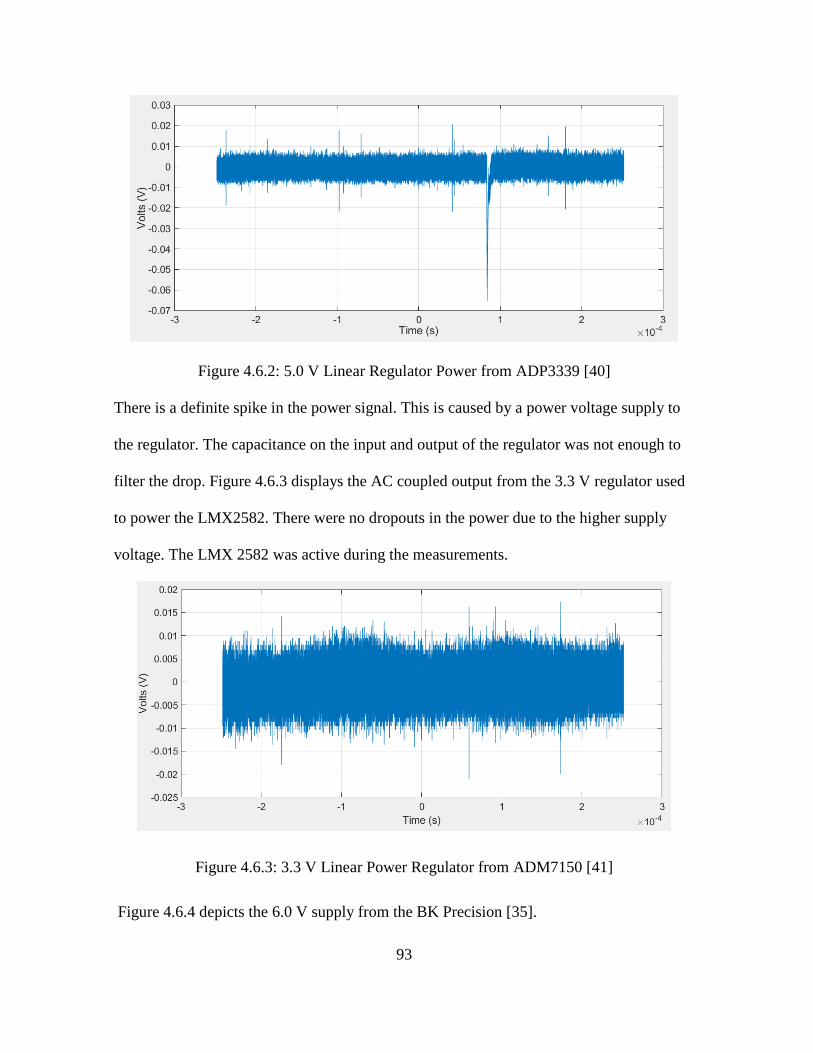
93
Figure 4.6.2: 5.0 V Linear Regulator Power from ADP3339 [40]
There is a definite spike in the power signal. This is caused by a power voltage supply to
the regulator. The capacitance on the input and output of the regulator was not enough to
filter the drop. Figure 4.6.3 displays the AC coupled output from the 3.3 V regulator used
to power the LMX2582. There were no dropouts in the power due to the higher supply
voltage. The LMX 2582 was active during the measurements.
Figure 4.6.3: 3.3 V Linear Power Regulator from ADM7150 [41]
Figure 4.6.4 depicts the 6.0 V supply from the BK Precision [35].
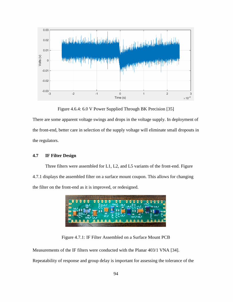
94
Figure 4.6.4: 6.0 V Power Supplied Through BK Precision [35]
There are some apparent voltage swings and drops in the voltage supply. In deployment of
the front-end, better care in selection of the supply voltage will eliminate small dropouts in
the regulators.
4.7 IF Filter Design
Three filters were assembled for L1, L2, and L5 variants of the front-end. Figure
4.7.1 displays the assembled filter on a surface mount coupon. This allows for changing
the filter on the front-end as it is improved, or redesigned.
Figure 4.7.1: IF Filter Assembled on a Surface Mount PCB
Measurements of the IF filters were conducted with the Planar 403/1 VNA [34].
Repeatability of response and group delay is important for assessing the tolerance of the
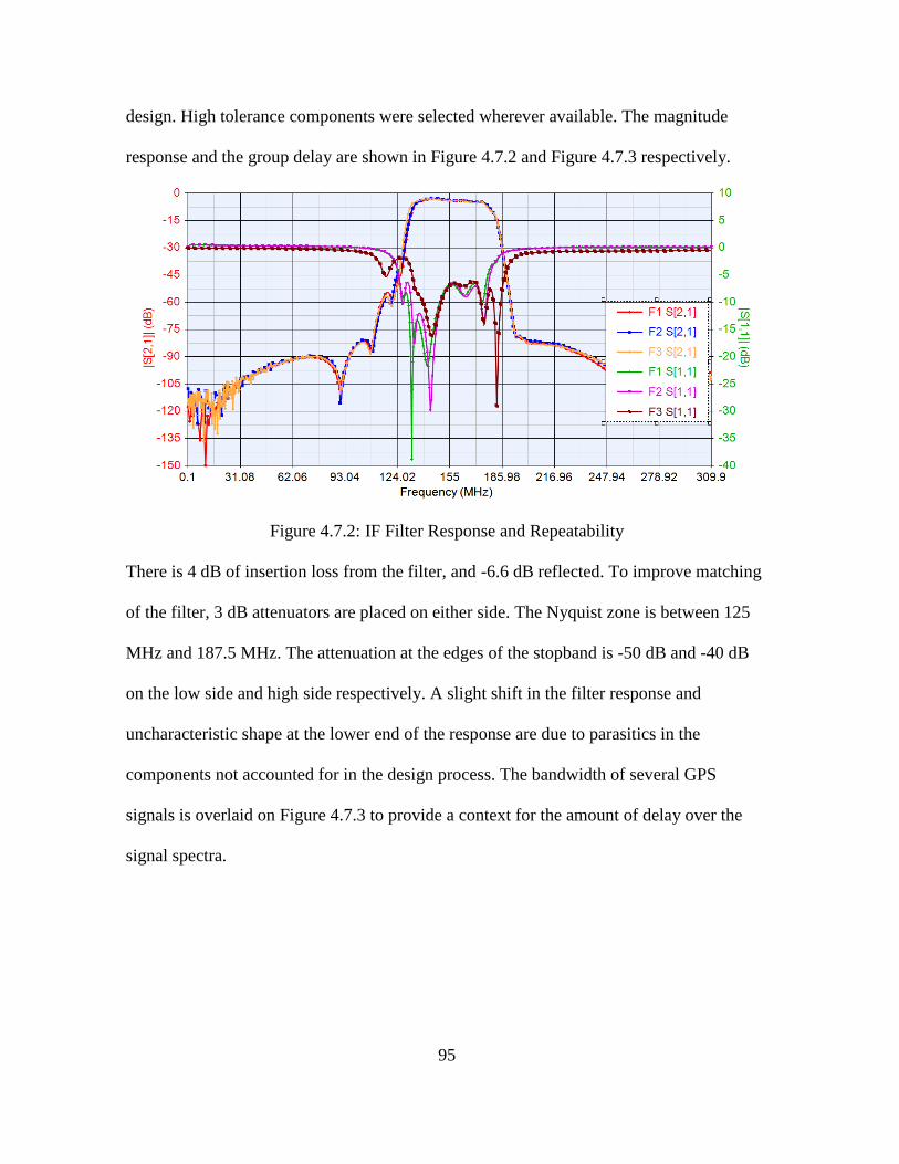
95
design. High tolerance components were selected wherever available. The magnitude
response and the group delay are shown in Figure 4.7.2 and Figure 4.7.3 respectively.
Figure 4.7.2: IF Filter Response and Repeatability
There is 4 dB of insertion loss from the filter, and -6.6 dB reflected. To improve matching
of the filter, 3 dB attenuators are placed on either side. The Nyquist zone is between 125
MHz and 187.5 MHz. The attenuation at the edges of the stopband is -50 dB and -40 dB
on the low side and high side respectively. A slight shift in the filter response and
uncharacteristic shape at the lower end of the response are due to parasitics in the
components not accounted for in the design process. The bandwidth of several GPS
signals is overlaid on Figure 4.7.3 to provide a context for the amount of delay over the
signal spectra.
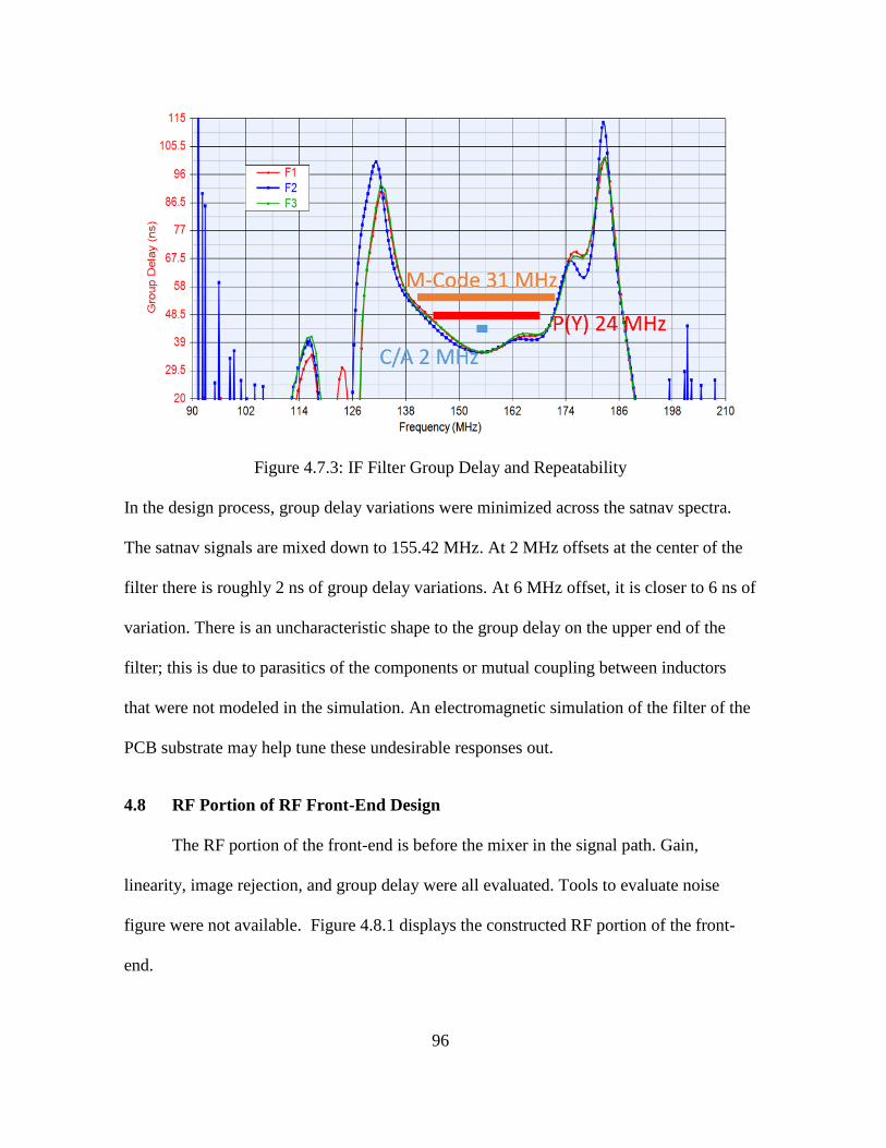
96
Figure 4.7.3: IF Filter Group Delay and Repeatability
In the design process, group delay variations were minimized across the satnav spectra.
The satnav signals are mixed down to 155.42 MHz. At 2 MHz offsets at the center of the
filter there is roughly 2 ns of group delay variations. At 6 MHz offset, it is closer to 6 ns of
variation. There is an uncharacteristic shape to the group delay on the upper end of the
filter; this is due to parasitics of the components or mutual coupling between inductors
that were not modeled in the simulation. An electromagnetic simulation of the filter of the
PCB substrate may help tune these undesirable responses out.
4.8 RF Portion of RF Front-End Design
The RF portion of the front-end is before the mixer in the signal path. Gain,
linearity, image rejection, and group delay were all evaluated. Tools to evaluate noise
figure were not available. Figure 4.8.1 displays the constructed RF portion of the front-
end.
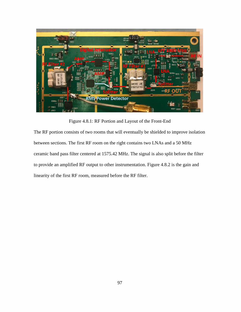
97
Figure 4.8.1: RF Portion and Layout of the Front-End
The RF portion consists of two rooms that will eventually be shielded to improve isolation
between sections. The first RF room on the right contains two LNAs and a 50 MHz
ceramic band pass filter centered at 1575.42 MHz. The signal is also split before the filter
to provide an amplified RF output to other instrumentation. Figure 4.8.2 is the gain and
linearity of the first RF room, measured before the RF filter.
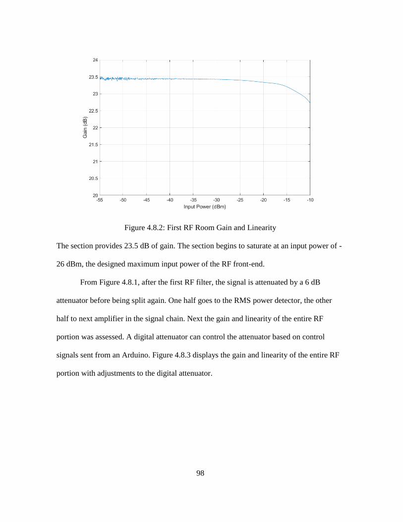
98
Figure 4.8.2: First RF Room Gain and Linearity
The section provides 23.5 dB of gain. The section begins to saturate at an input power of -
26 dBm, the designed maximum input power of the RF front-end.
From Figure 4.8.1, after the first RF filter, the signal is attenuated by a 6 dB
attenuator before being split again. One half goes to the RMS power detector, the other
half to next amplifier in the signal chain. Next the gain and linearity of the entire RF
portion was assessed. A digital attenuator can control the attenuator based on control
signals sent from an Arduino. Figure 4.8.3 displays the gain and linearity of the entire RF
portion with adjustments to the digital attenuator.
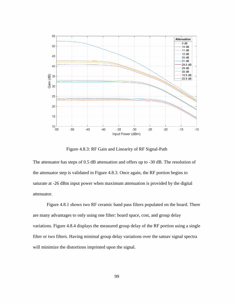
99
Figure 4.8.3: RF Gain and Linearity of RF Signal-Path
The attenuator has steps of 0.5 dB attenuation and offers up to -30 dB. The resolution of
the attenuator step is validated in Figure 4.8.3. Once again, the RF portion begins to
saturate at -26 dBm input power when maximum attenuation is provided by the digital
attenuator.
Figure 4.8.1 shows two RF ceramic band pass filters populated on the board. There
are many advantages to only using one filter: board space, cost, and group delay
variations. Figure 4.8.4 displays the measured group delay of the RF portion using a single
filter or two filters. Having minimal group delay variations over the satnav signal spectra
will minimize the distortions imprinted upon the signal.
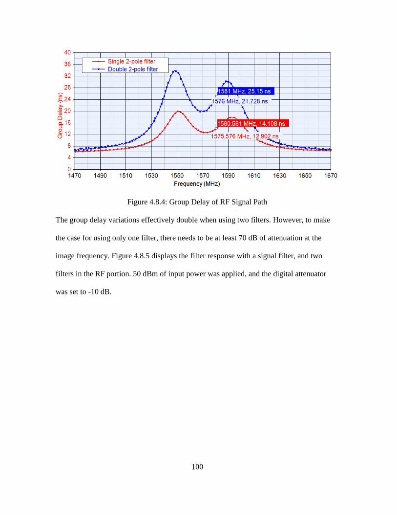
100
Figure 4.8.4: Group Delay of RF Signal Path
The group delay variations effectively double when using two filters. However, to make
the case for using only one filter, there needs to be at least 70 dB of attenuation at the
image frequency. Figure 4.8.5 displays the filter response with a signal filter, and two
filters in the RF portion. 50 dBm of input power was applied, and the digital attenuator
was set to -10 dB.
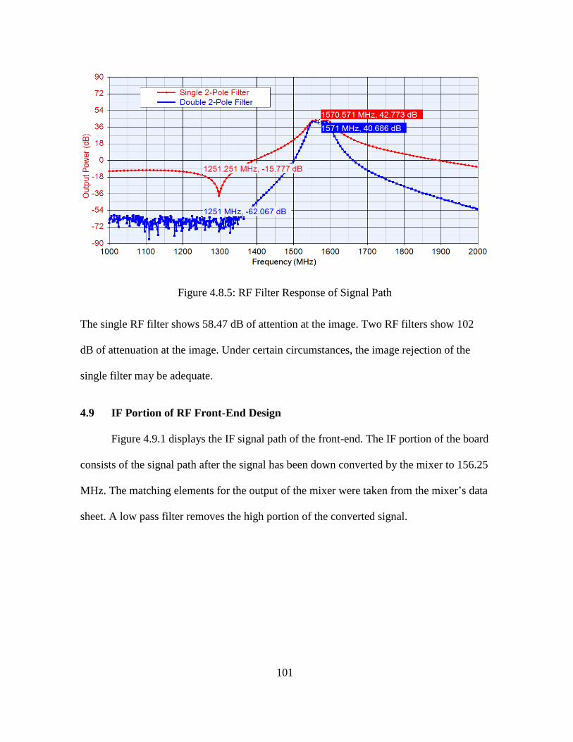
101
Figure 4.8.5: RF Filter Response of Signal Path
The single RF filter shows 58.47 dB of attention at the image. Two RF filters show 102
dB of attenuation at the image. Under certain circumstances, the image rejection of the
single filter may be adequate.
4.9 IF Portion of RF Front-End Design
Figure 4.9.1 displays the IF signal path of the front-end. The IF portion of the board
consists of the signal path after the signal has been down converted by the mixer to 156.25
MHz. The matching elements for the output of the mixer were taken from the mixer’s data
sheet. A low pass filter removes the high portion of the converted signal.
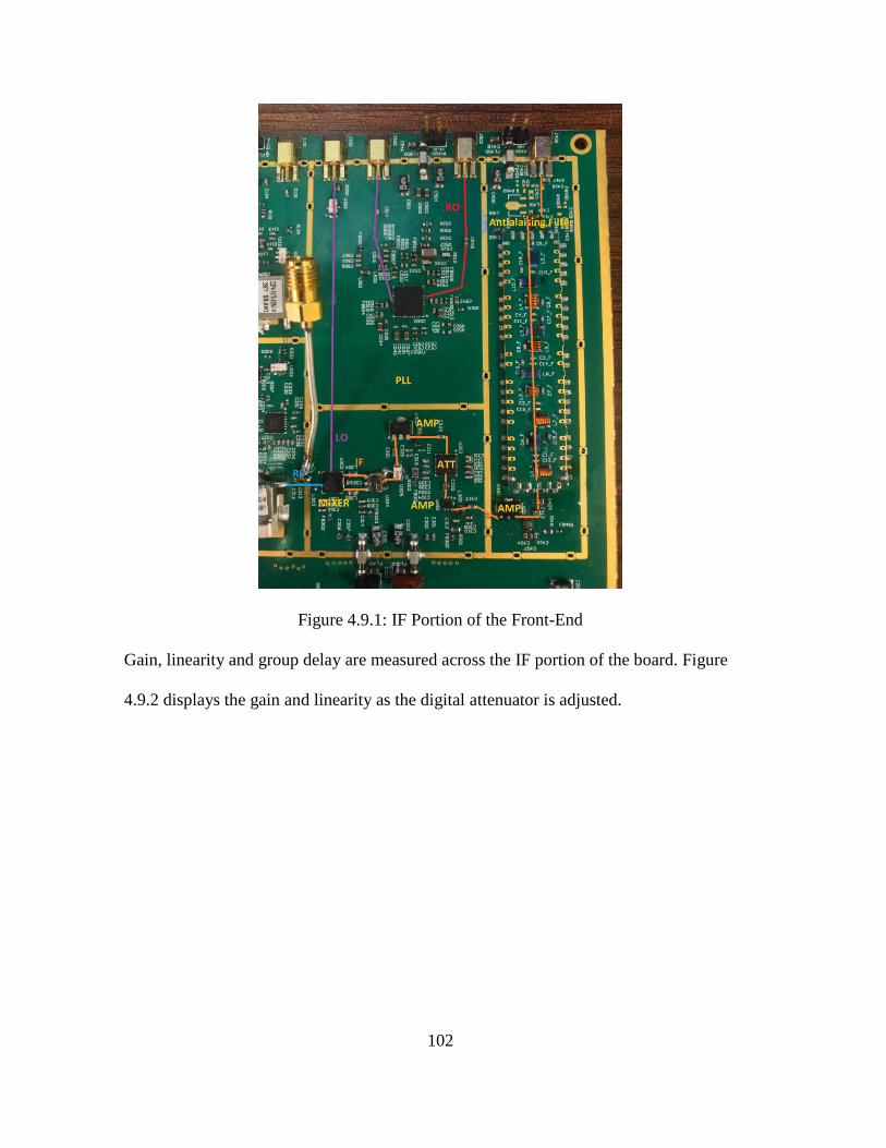
102
Figure 4.9.1: IF Portion of the Front-End
Gain, linearity and group delay are measured across the IF portion of the board. Figure
4.9.2 displays the gain and linearity as the digital attenuator is adjusted.

103
Figure 4.9.2: IF Portion Gain and Linearity of the Front-End
The RF portion of the board can supply a maximum of -7 dBm of power to the IF section,
when under the duress of 100 dB J/S. The TQP369182 is the first amplifier in the signal
path in the IF portion, thus it must handle the maximum input of power of -7 dBm without
saturating. The TQP369182 has 15.1 dBm P1dB output power and 21 dB of gain, the max
input power is -6 dBm. Thus, the device will operate in its linear region under the
maximum -7 dBm. However, Figure 4.9.2 shows that IF portion can only handle a
maximum -25 dBm of input power before saturating. This is due to the amplifier that was
populated before the IF filter. This amplifier was not included in the simulation of the
front-end, and will have the option to be excluded in future revisions.
Figure 4.9.3 displays the IF filter response and the group delay of the IF portion of
the board. The input power was -40 dBm, and the attenuator was set to 20 dB.
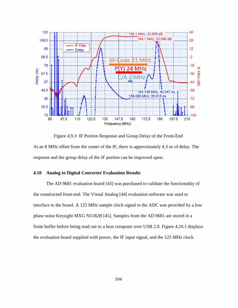
104
Figure 4.9.3: IF Portion Response and Group Delay of the Front-End
At an 8 MHz offset from the center of the IF, there is approximately 4.3 ns of delay. The
response and the group delay of the IF portion can be improved upon.
4.10 Analog to Digital Converter Evaluation Results
The AD 9681 evaluation board [43] was purchased to validate the functionality of
the constructed front-end. The Visual Analog [44] evaluation software was used to
interface to the board. A 125 MHz sample clock signal to the ADC was provided by a low
phase noise Keysight MXG N5182B [45]. Samples from the AD 9681 are stored in a
finite buffer before being read out to a host computer over USB 2.0. Figure 4.10.1 displays
the evaluation board supplied with power, the IF input signal, and the 125 MHz clock.
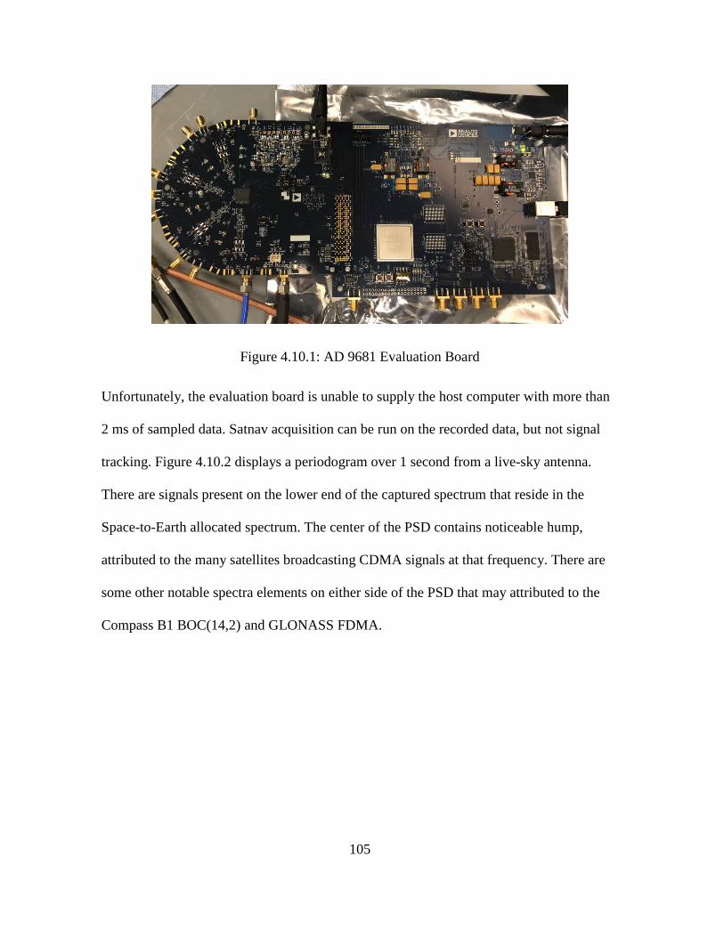
105
Figure 4.10.1: AD 9681 Evaluation Board
Unfortunately, the evaluation board is unable to supply the host computer with more than
2 ms of sampled data. Satnav acquisition can be run on the recorded data, but not signal
tracking. Figure 4.10.2 displays a periodogram over 1 second from a live-sky antenna.
There are signals present on the lower end of the captured spectrum that reside in the
Space-to-Earth allocated spectrum. The center of the PSD contains noticeable hump,
attributed to the many satellites broadcasting CDMA signals at that frequency. There are
some other notable spectra elements on either side of the PSD that may attributed to the
Compass B1 BOC(14,2) and GLONASS FDMA.

106
Figure 4.10.2: ADC PSD from Live-sky Antenna
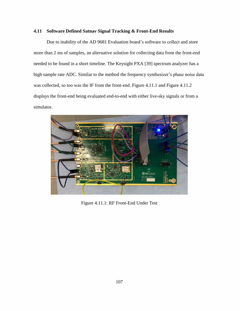
107
4.11 Software Defined Satnav Signal Tracking & Front-End Results
Due to inability of the AD 9681 Evaluation board’s software to collect and store
more than 2 ms of samples, an alternative solution for collecting data from the front-end
needed to be found in a short timeline. The Keysight PXA [39] spectrum analyzer has a
high sample rate ADC. Similar to the method the frequency synthesizer’s phase noise data
was collected, so too was the IF from the front-end. Figure 4.11.1 and Figure 4.11.2
displays the front-end being evaluated end-to-end with either live-sky signals or from a
simulator.
Figure 4.11.1: RF Front-End Under Test
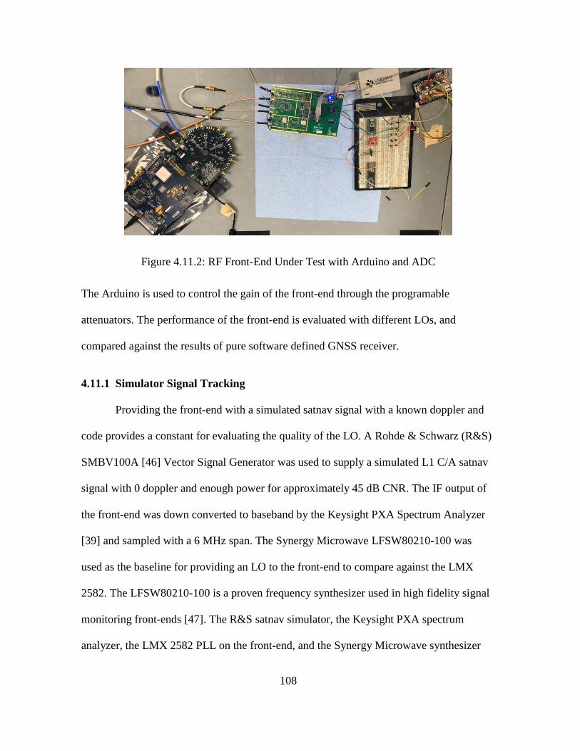
108
Figure 4.11.2: RF Front-End Under Test with Arduino and ADC
The Arduino is used to control the gain of the front-end through the programable
attenuators. The performance of the front-end is evaluated with different LOs, and
compared against the results of pure software defined GNSS receiver.
4.11.1 Simulator Signal Tracking
Providing the front-end with a simulated satnav signal with a known doppler and
code provides a constant for evaluating the quality of the LO. A Rohde & Schwarz (R&S)
SMBV100A [46] Vector Signal Generator was used to supply a simulated L1 C/A satnav
signal with 0 doppler and enough power for approximately 45 dB CNR. The IF output of
the front-end was down converted to baseband by the Keysight PXA Spectrum Analyzer
[39] and sampled with a 6 MHz span. The Synergy Microwave LFSW80210-100 was
used as the baseline for providing an LO to the front-end to compare against the LMX
2582. The LFSW80210-100 is a proven frequency synthesizer used in high fidelity signal
monitoring front-ends [47]. The R&S satnav simulator, the Keysight PXA spectrum
analyzer, the LMX 2582 PLL on the front-end, and the Synergy Microwave synthesizer
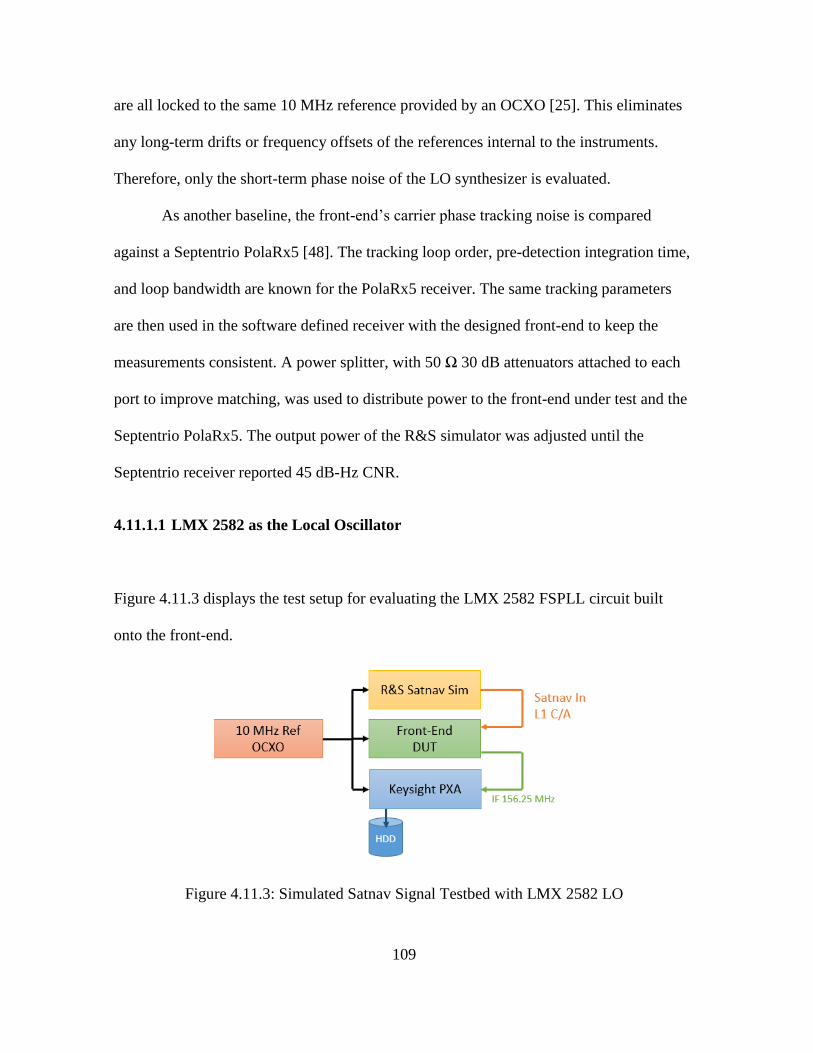
109
are all locked to the same 10 MHz reference provided by an OCXO [25]. This eliminates
any long-term drifts or frequency offsets of the references internal to the instruments.
Therefore, only the short-term phase noise of the LO synthesizer is evaluated.
As another baseline, the front-end’s carrier phase tracking noise is compared
against a Septentrio PolaRx5 [48]. The tracking loop order, pre-detection integration time,
and loop bandwidth are known for the PolaRx5 receiver. The same tracking parameters
are then used in the software defined receiver with the designed front-end to keep the
measurements consistent. A power splitter, with 50 Ω 30 dB attenuators attached to each
port to improve matching, was used to distribute power to the front-end under test and the
Septentrio PolaRx5. The output power of the R&S simulator was adjusted until the
Septentrio receiver reported 45 dB-Hz CNR.
4.11.1.1 LMX 2582 as the Local Oscillator
Figure 4.11.3 displays the test setup for evaluating the LMX 2582 FSPLL circuit built
onto the front-end.
Figure 4.11.3: Simulated Satnav Signal Testbed with LMX 2582 LO
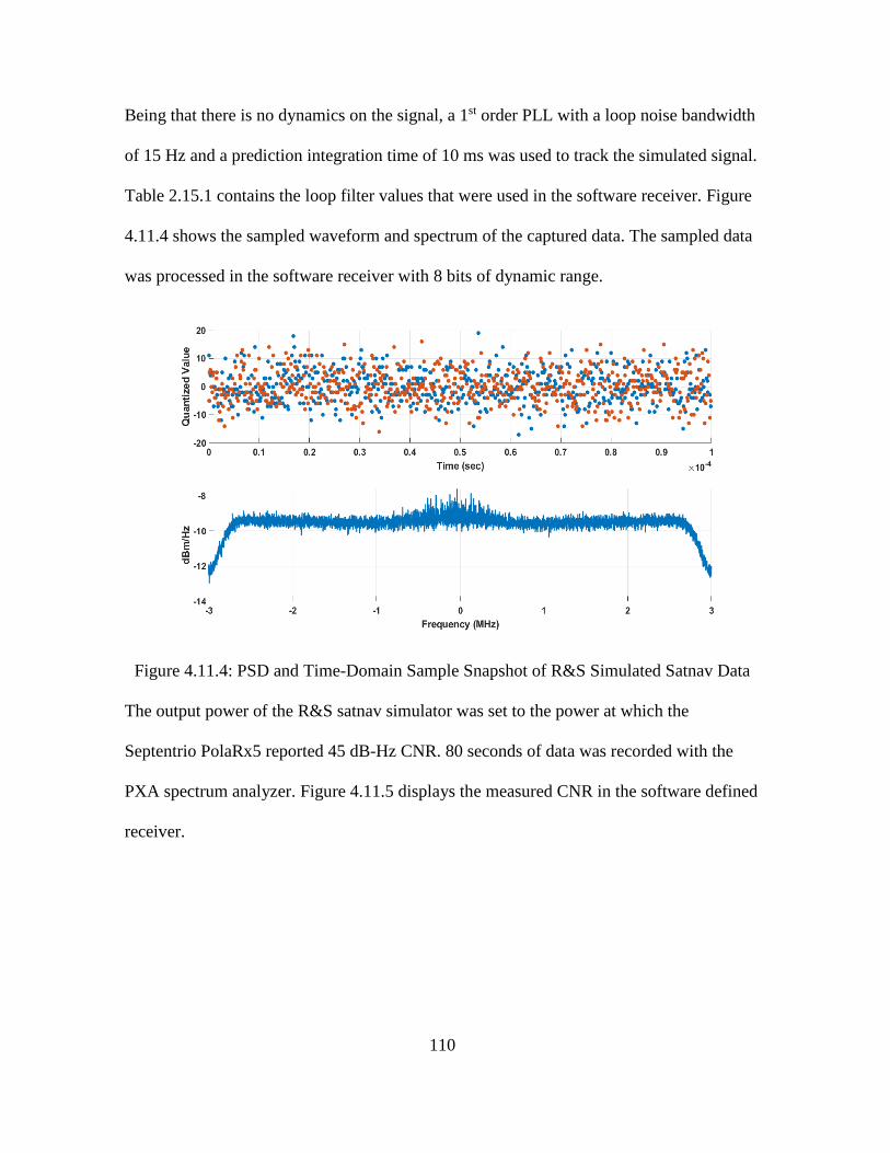
110
Being that there is no dynamics on the signal, a 1st order PLL with a loop noise bandwidth
of 15 Hz and a prediction integration time of 10 ms was used to track the simulated signal.
Table 2.15.1 contains the loop filter values that were used in the software receiver. Figure
4.11.4 shows the sampled waveform and spectrum of the captured data. The sampled data
was processed in the software receiver with 8 bits of dynamic range.
Figure 4.11.4: PSD and Time-Domain Sample Snapshot of R&S Simulated Satnav Data
The output power of the R&S satnav simulator was set to the power at which the
Septentrio PolaRx5 reported 45 dB-Hz CNR. 80 seconds of data was recorded with the
PXA spectrum analyzer. Figure 4.11.5 displays the measured CNR in the software defined
receiver.
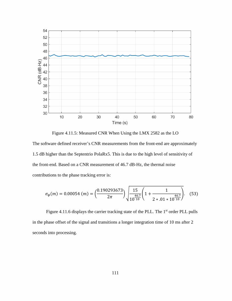
111
Figure 4.11.5: Measured CNR When Using the LMX 2582 as the LO
The software defined receiver’s CNR measurements from the front-end are approximately
1.5 dB higher than the Septentrio PolaRx5. This is due to the high level of sensitivity of
the front-end. Based on a CNR measurement of 46.7 dB-Hz, the thermal noise
contributions to the phase tracking error is:
𝜎𝜙(𝑚) = 0.00054 (𝑚) = (0.190293673
2𝜋) √
15
1046.710
(1 +1
2 ∗ .01 ∗ 1046.710
). (53)
Figure 4.11.6 displays the carrier tracking state of the PLL. The 1st order PLL pulls
in the phase offset of the signal and transitions a longer integration time of 10 ms after 2
seconds into processing.
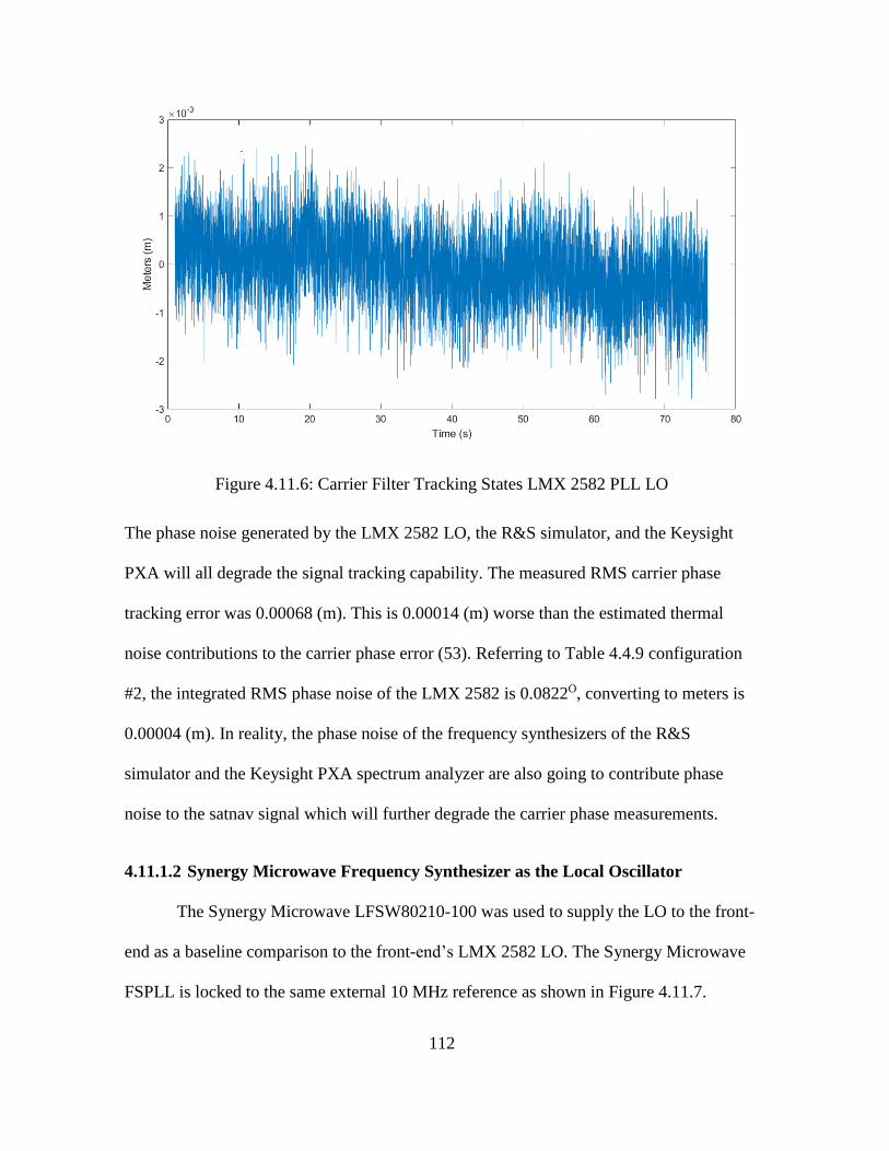
112
Figure 4.11.6: Carrier Filter Tracking States LMX 2582 PLL LO
The phase noise generated by the LMX 2582 LO, the R&S simulator, and the Keysight
PXA will all degrade the signal tracking capability. The measured RMS carrier phase
tracking error was 0.00068 (m). This is 0.00014 (m) worse than the estimated thermal
noise contributions to the carrier phase error (53). Referring to Table 4.4.9 configuration
#2, the integrated RMS phase noise of the LMX 2582 is 0.0822O, converting to meters is
0.00004 (m). In reality, the phase noise of the frequency synthesizers of the R&S
simulator and the Keysight PXA spectrum analyzer are also going to contribute phase
noise to the satnav signal which will further degrade the carrier phase measurements.
4.11.1.2 Synergy Microwave Frequency Synthesizer as the Local Oscillator
The Synergy Microwave LFSW80210-100 was used to supply the LO to the front-
end as a baseline comparison to the front-end’s LMX 2582 LO. The Synergy Microwave
FSPLL is locked to the same external 10 MHz reference as shown in Figure 4.11.7.
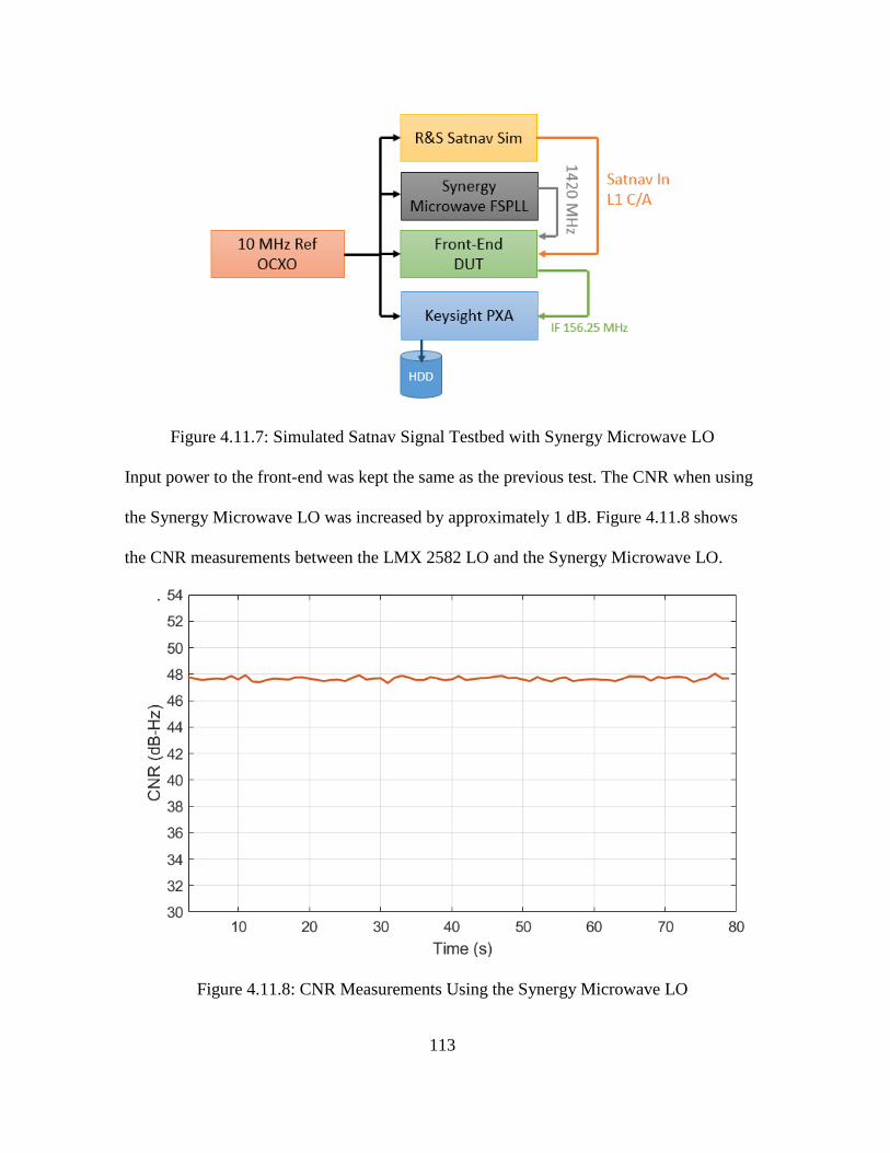
113
Figure 4.11.7: Simulated Satnav Signal Testbed with Synergy Microwave LO
Input power to the front-end was kept the same as the previous test. The CNR when using
the Synergy Microwave LO was increased by approximately 1 dB. Figure 4.11.8 shows
the CNR measurements between the LMX 2582 LO and the Synergy Microwave LO.
Figure 4.11.8: CNR Measurements Using the Synergy Microwave LO

114
The improved CNR is due to better phase noise and spur performance of the Synergy
Microwave over the LMX 2582. The RMS phase tracking error can again be estimated
through:
𝜎𝜙(𝑚) = 0.00049 (𝑚) = (0.190293673
2𝜋) √
15
1047.710
(1 +1
2 ∗ .01 ∗ 1047.710
). (54)
Figure 4.11.9 displays the carrier filter tracking states using the Synergy Microwave as the
LO to the front-end. The same tracking parameters were used in the software defined
receiver from testing the LMX 2582 as the LO.
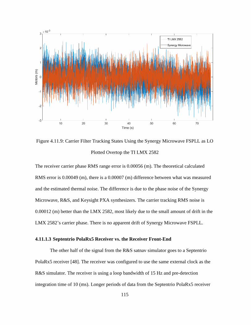
115
Figure 4.11.9: Carrier Filter Tracking States Using the Synergy Microwave FSPLL as LO
Plotted Overtop the TI LMX 2582
The receiver carrier phase RMS range error is 0.00056 (m). The theoretical calculated
RMS error is 0.00049 (m), there is a 0.00007 (m) difference between what was measured
and the estimated thermal noise. The difference is due to the phase noise of the Synergy
Microwave, R&S, and Keysight PXA synthesizers. The carrier tracking RMS noise is
0.00012 (m) better than the LMX 2582, most likely due to the small amount of drift in the
LMX 2582’s carrier phase. There is no apparent drift of Synergy Microwave FSPLL.
4.11.1.3 Septentrio PolaRx5 Receiver vs. the Receiver Front-End
The other half of the signal from the R&S satnav simulator goes to a Septentrio
PolaRx5 receiver [48]. The receiver was configured to use the same external clock as the
R&S simulator. The receiver is using a loop bandwidth of 15 Hz and pre-detection
integration time of 10 (ms). Longer periods of data from the Septentrio PolaRx5 receiver
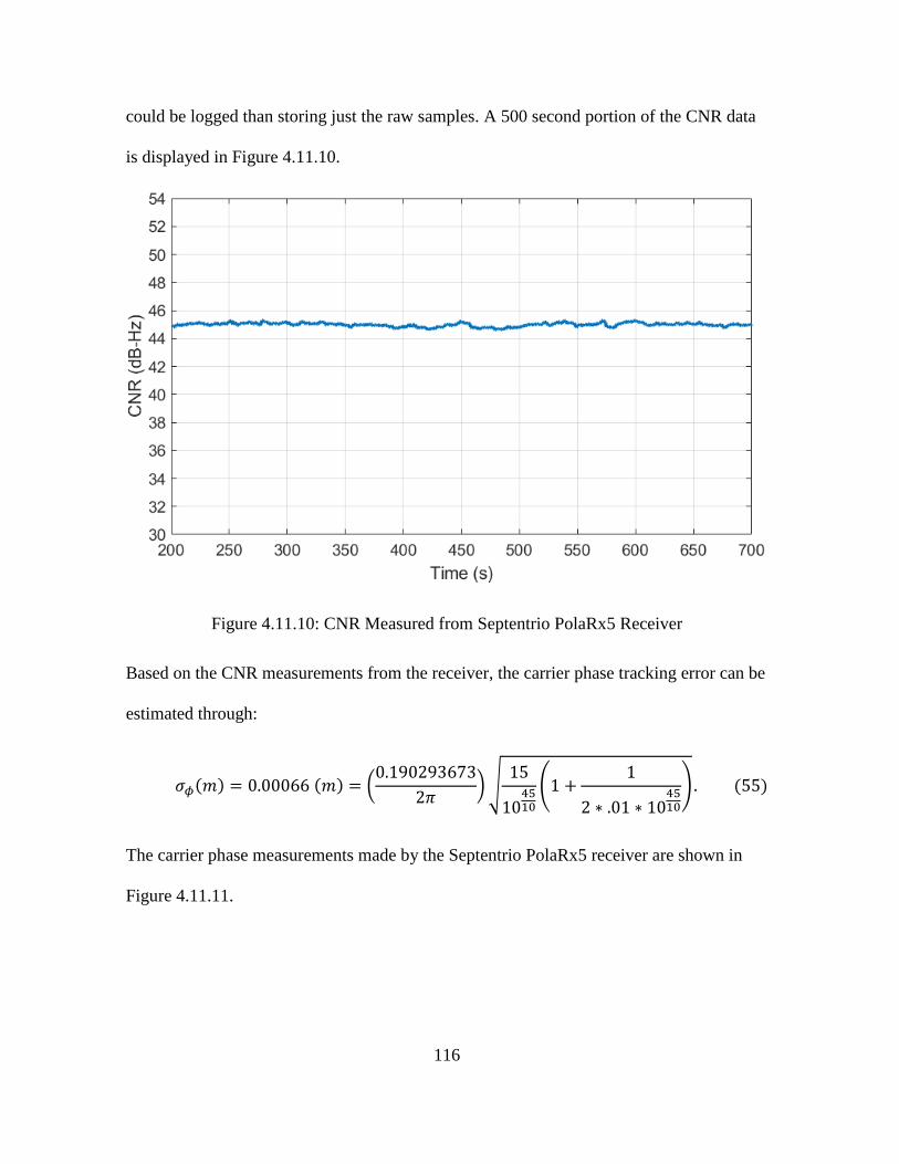
116
could be logged than storing just the raw samples. A 500 second portion of the CNR data
is displayed in Figure 4.11.10.
Figure 4.11.10: CNR Measured from Septentrio PolaRx5 Receiver
Based on the CNR measurements from the receiver, the carrier phase tracking error can be
estimated through:
𝜎𝜙(𝑚) = 0.00066 (𝑚) = (0.190293673
2𝜋) √
15
104510
(1 +1
2 ∗ .01 ∗ 104510
). (55)
The carrier phase measurements made by the Septentrio PolaRx5 receiver are shown in
Figure 4.11.11.
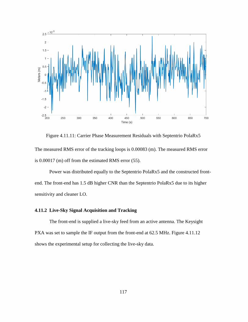
117
Figure 4.11.11: Carrier Phase Measurement Residuals with Septentrio PolaRx5
The measured RMS error of the tracking loops is 0.00083 (m). The measured RMS error
is 0.00017 (m) off from the estimated RMS error (55).
Power was distributed equally to the Septentrio PolaRx5 and the constructed front-
end. The front-end has 1.5 dB higher CNR than the Septentrio PolaRx5 due to its higher
sensitivity and cleaner LO.
4.11.2 Live-Sky Signal Acquisition and Tracking
The front-end is supplied a live-sky feed from an active antenna. The Keysight
PXA was set to sample the IF output from the front-end at 62.5 MHz. Figure 4.11.12
shows the experimental setup for collecting the live-sky data.

118
Figure 4.11.12: Live-sky Satnav Signal with LMX 2582 LO
Due to memory constraints of the PXA, only 19 seconds worth of data could be recorded
at 62.5 MHz. Figure 4.11.13 displays the calculated PSD from averaging.
Figure 4.11.13: L1-Band Live-sky Capture 62.5 MHz of Bandwidth PSD
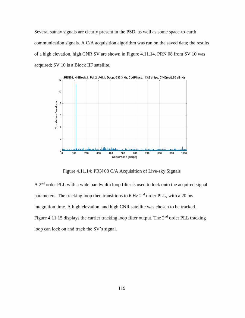
119
Several satnav signals are clearly present in the PSD, as well as some space-to-earth
communication signals. A C/A acquisition algorithm was run on the saved data; the results
of a high elevation, high CNR SV are shown in Figure 4.11.14. PRN 08 from SV 10 was
acquired; SV 10 is a Block IIF satellite.
Figure 4.11.14: PRN 08 C/A Acquisition of Live-sky Signals
A 2nd order PLL with a wide bandwidth loop filter is used to lock onto the acquired signal
parameters. The tracking loop then transitions to 6 Hz 2nd order PLL, with a 20 ms
integration time. A high elevation, and high CNR satellite was chosen to be tracked.
Figure 4.11.15 displays the carrier tracking loop filter output. The 2nd order PLL tracking
loop can lock on and track the SV’s signal.
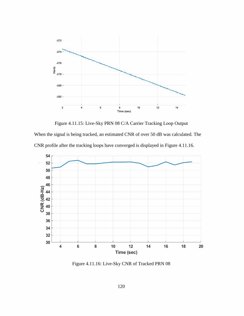
120
Figure 4.11.15: Live-Sky PRN 08 C/A Carrier Tracking Loop Output
When the signal is being tracked, an estimated CNR of over 50 dB was calculated. The
CNR profile after the tracking loops have converged is displayed in Figure 4.11.16.
Figure 4.11.16: Live-Sky CNR of Tracked PRN 08
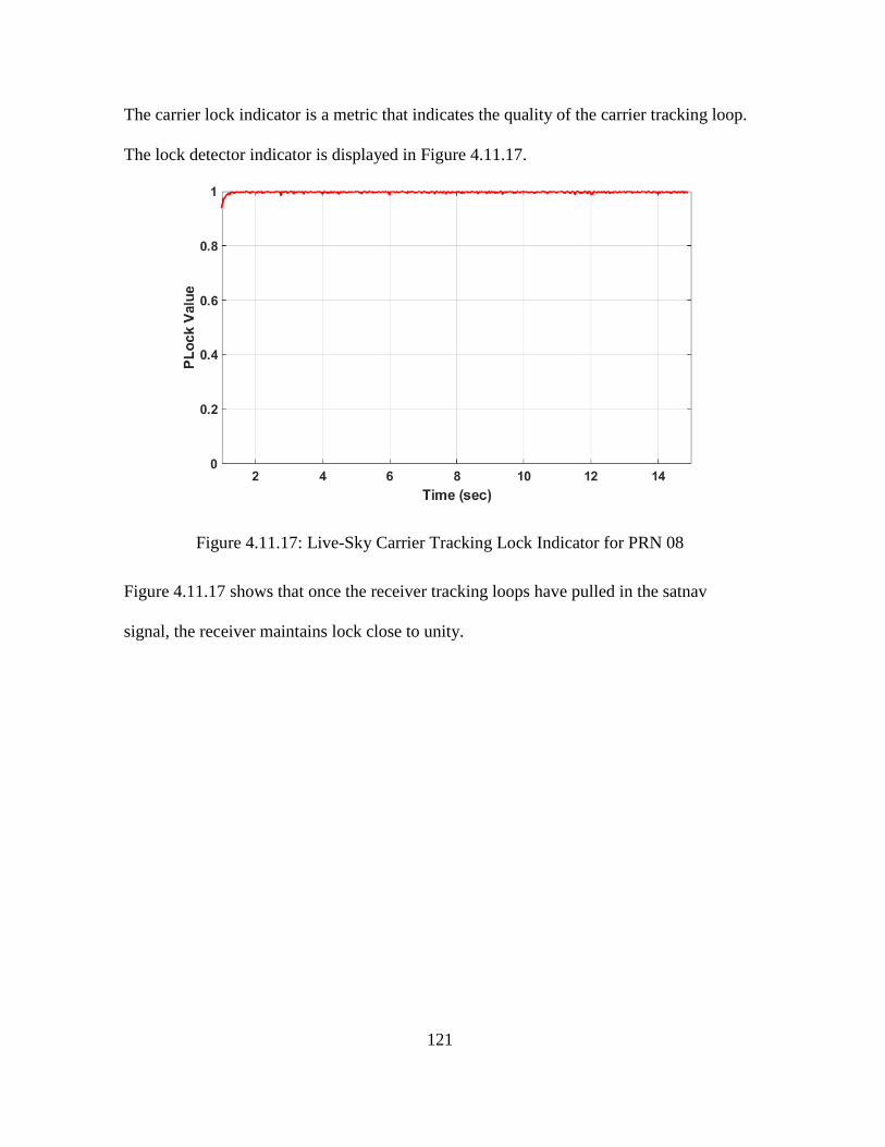
121
The carrier lock indicator is a metric that indicates the quality of the carrier tracking loop.
The lock detector indicator is displayed in Figure 4.11.17.
Figure 4.11.17: Live-Sky Carrier Tracking Lock Indicator for PRN 08
Figure 4.11.17 shows that once the receiver tracking loops have pulled in the satnav
signal, the receiver maintains lock close to unity.
122
V. Conclusions and Recommendations
5.1 Conclusions of Research
A wideband instrumentation satnav front-end was designed for the purpose of high-
fidelity signal and spectrum monitoring. The initial testing shows that this receiver meets
the requirements. Several major achievements were met in this study:
A validated frequency plan that is compatible with today’s state of the art multi-
channel ADCs.
A Wide 50 MHz+ usable bandwidth supports M-Code and other wideband signal
monitoring.
Higher performance RF component selections and evaluations.
RMS Power detector to accurately sense power before the mixer.
High dynamic range to support use in high interference environments.
Designed to support up to 100 dB J/S.
Support for smart software-based gain control for preserving front-end linearity in
the presence of high interference.
High isolation RF PCB design using grounded coplanar waveguide.
Temperature sensors at RF and IF stages to monitor and apply temperature
compensation for temperature-induced group delay variations.
Multiple configuration support. Multi-element, and multi-band coherent LO
distribution.
Design for high sensitivity, low phase noise, and low group delay.
123
3U Open VPX form factor to support modular assembly of various high-fidelity
satnav SDR configurations for research as well as long-term deployment.
Discrete LC IF filter design, characterization, and testing.
Testing and validating the target ADC through the evaluation board.
Satnav simulator and live-sky signal acquisition and tracking.
Individual testing and characterization of group delay and linearity of the RF
rooms using the VNA.
Initial PCB and assembly of the front-end worked without any major
modifications.
More quantitative analysis of the front-end developed in this study is required.
Satnav professionals demand a vetted and calibrated front-end for trusted nominal
measurements. It is expected that this front-end design will meet these demanding
requirements after careful analysis, characterization and additional
revision/implementation/testing cycles.
5.2 Significance of Research
The design of the front-end can provide a baseline for technology transfer to other
research labs or field use. As signal quality and spectrum monitoring becomes more
pervasive and desirable, the design methodology, lessons-learned and contributions made
through this research effort will hopefully serve as a baseline. The receiver can provide
nominal signal characteristics which can enable advanced satnav signal monitoring and
precision location and timing.
124
5.3 Recommendations for Future Research
To truly call this an instrumentation-grade satnav front-end, more focus on the
FSPLL is needed. Initial testing revealed some close-in spurs at 60 Hz and 120 Hz which
may be detrimental to tracking performance. Using an external VCO that has a frequency
output from 1-2 GHz can greatly improve phase noise due to the lower N feedback
division ratio required. A dual-loop FSPLL and increasing the RO frequency can improve
spurious emissions and further reduce the phase noise. The downside of course is space
and power consumption.
Software development is needed to sense the input power from either the ADC or
the RMS power detector and adjust the RF and IF stage digital attenuators. Attenuation
needs to be applied, adjusted, and logged during signal collections to preserve linearity.
The group delay variations of the IF bandpass filter can be greatly improved.
Currently a 9th order bandpass filter is implemented. By lowering the filter order, group
delay variations over the pass band can be reduced. The frequency response can also use
some improvement. However, by characterizing the group delay and magnitude response
of the front-end with the VNA, pre-processing can be applied to the sampled signal in
order to remove group delay variations.
For advanced timing receivers, pseudorange biases caused by temperature changes
in the front-end may be a problem. This can add larger variances to the time at longer
sample intervals. By building temperature profiles for the front-end, the biases can be
removed at either the baseband signal processing stage or post pseudorange computation
stage. The sensitive temperature sensors built into this front-end can be leveraged
eventually to implement this functionality.

125
Direct conversion and direct sampling receivers have become extremely popular in
satnav front-ends. An in-depth comparison between practical receivers based on these
front-end architecture types can benefit the academic and industrial communities.
5.4 Summary
For this research, a satnav receiver front-end was modeled, designed, assembled,
and tested over the span of 6 months. The front-end’s group delay variations over the
passband are lower than those of other receiver front-ends that have been previously
implemented [47]. The phase noise and spurs from the FSPLL have been minimized
through the design process. Digital gain control capabilities are included to keep the
receiver operating in its linear region in high-interference environments.

126
Appendices
Appendix A: PCB Stack Up
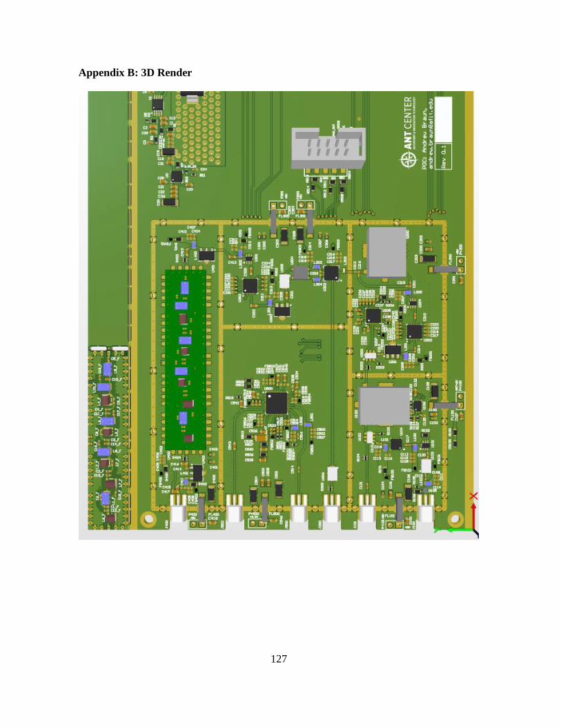
127
Appendix B: 3D Render

128
Bibliography
[1] S. Gunawardena, J. Raquet, and F. Van Graas, “A satellite with personality: Chip
transition-edge based signal tracking for ultra-precise GNSS monitoring
applications,” GPS World, vol. 26, no. 8, pp. 38–43, 2015.
[2] S. Thombre, N. N. Tchamov, S. Lohan, M. Valkama, and J. Nurmi, “Effects of
radio front-end PLL phase noise on GNSS baseband correlation,” Navig. J. Inst.
Navig., vol. 61, no. 1, pp. 13–21, 2014.
[3] S. Gunawardena and F. Van Graas, “GPS-SPS Inter-PRN Pseudorange Biases
compared for Transversal SAW and LC Filters using Live Sky Data and ChipShape
Software Receiver Processing,” in Proceedings of the 2015 International Technical
Meeting, 2015, pp. 393–403.
[4] J. M. Guerrero and S. Gunawardena, “Characterization of Timing and Pseudorange
Biases Due to GNSS Front-End Filters by Type, Temperature, and Doppler
Frequency,” in Proceedings of the 2017 International Technical Meeting of The
Institute of Navigation, 2018, pp. 418–444.
[5] J. W. Betz, Engineering Satellite-Based Navigation and Timing: Global Navigation
Satellite Systems, Signals, and Receivers. Piscataway, NJ: IEEE Press, 2016.
[6] T. J. Rouphael, Wireless Receiver Architectures and Design: Antennas, RF,
Synthesizers, Mixed Signal, and Digital Signal Processing. Waltham: Elsevier,
2014.
[7] M. L. Psiaki and D. M. Akos, “A Comparison of ‘ Direct RF Sampling ’ and ‘
Down-Convert & Sampling ’ GNSS Receiver Architectures,” 16th Int. Satell. Div.
Inst. Navig. Tech. Meet., pp. 1941–1952, 2003.
129
[8] R. G. Brown and P. Y. C. Hwang, Introduction to Random Signals and Applied
Kalman Filtering. Wiley, 1992.
[9] J. Ó. Winkel, “Modeling and Simulating GNSS Signal Structures and Receivers,”
Signals, pp. 1–247, 2000.
[10] W. Yu, G. Lachapelle, and S. Skone, “PLL Performance for Signals in the Presence
of Thermal Noise, Phase Noise, and Ionospheric Scintillation,” in Proceedings of
the 19th International Technical Meeting of the Satellite Division of The Institute of
Navigation (ION GNSS 2006), 2006, no. September, pp. 1341–1357.
[11] W. J. Riley, Handbook of Frequency Stability Analysis, vol. 31, no. 1. NIST, 1994.
[12] D. Banerjee, PLL Performance, Simulation, and Design, Fith Edition. 2017.
[13] A. Demir, “Phase noise and timing jitter in oscillators with colored-noise sources,”
IEEE Trans. Circuits Syst. I Fundam. Theory Appl., vol. 49, no. 12, pp. 1782–1791,
2002.
[14] P. Mathecken, T. Riihonen, N. N. Tchamov, S. Werner, M. Valkama, and R.
Wichman, “Characterization of OFDM radio link under PLL-based oscillator phase
noise and multipath fading channel,” IEEE Trans. Commun., vol. 60, no. 6, pp.
1479–1485, 2012.
[15] “Texas Instruments LMX2582 Wideband PLLatinum RF Synthesizer With
Integrated VCO,” 2017. [Online]. Available:
http://www.ti.com/lit/ds/symlink/lmx2582.pdf. [Accessed: 07-Nov-2018].
[16] S. Gunawardena and F. Van Graas, “Analysis of GPS-SPS Inter-PRN Pseudorange
Biases due to Receiver Front-End Components,” in Proc. Of the 27th International
Technical Meeting of ION GNSS-2014, 2014.
130
[17] E. D. Kaplan and C. J. Hegarty, Understanding GPS/GNSS Principals and
Applications, Third Edition. Boston: Artech House, 2017.
[18] M. Irsigler and B. Eissfeller, “PLL Tracking Performance in the Presence of
Oscillator Phase Noise,” GPS Solut., vol. 5, no. 4, pp. 45–57, 2002.
[19] J. J. Spilker, Digital Communications by Satellite. Englewood Cliffs, NJ: Prentice
Hall, 1977.
[20] P. Enge and P. Misra, Global Positioning System: Signals, Measurements, and
Performance - Revised Second Edition (2011), no. 2. 2011.
[21] J. J. Spilker, P. Axelrad, B. W. Parkinson, and P. Enge, “‘GPS Receivers’, Global
Positioning System: Theory and Applications, Volume I,” Progress in Astronautics
and Aeronautics, 1996, pp. 329–407.
[22] “AD9681.” [Online]. Available: https://www.analog.com/media/en/technical-
documentation/data-sheets/ad9681.pdf. [Accessed: 02-Feb-2019].
[23] “Modelithics.” [Online]. Available: https://www.modelithics.com/. [Accessed: 02-
Feb-2019].
[24] “Genesys Vendor Parts Synthesis.” [Online]. Available:
https://www.keysight.com/main/editorial.jspx?cc=US&lc=eng&ckey=2965156&ni
d=-34275.0.00&id=2965156&cmpid=zzfindeesof-genesys-vps. [Accessed: 02-Feb-
2019].
[25] “Wenzel BTULN 501-27503-35.” [Online]. Available:
http://www.wenzel.com/model/btuln/. [Accessed: 07-Nov-2018].
[26] C. W. Sayre, Complete Wireless Design, Second Edition. McGraw-Hill, 2008.
[27] “HMC542BLP4E.” [Online]. Available:
131
https://www.analog.com/media/en/technical-documentation/data-
sheets/hmc542b.pdf. [Accessed: 02-Feb-2019].
[28] “HMC1020LP4E.” [Online]. Available:
https://www.analog.com/media/en/technical-documentation/data-
sheets/hmc1020.pdf. [Accessed: 02-Feb-2019].
[29] “MAAL-010704.” [Online]. Available: https://www.macom.com/products/product-
detail/MAAL-010704. [Accessed: 14-Jan-2019].
[30] “TQP3M9005.” [Online]. Available:
https://www.qorvo.com/products/p/TQP3M9005. [Accessed: 02-Feb-2019].
[31] “SnP (Touchstone) File Format.” [Online]. Available:
http://na.support.keysight.com/plts/help/WebHelp/FilePrint/SnP_File_Format.htm.
[Accessed: 02-Feb-2019].
[32] “RO4003C Laminates.” [Online]. Available:
http://www.rogerscorp.com/acs/products/54/ro4003c-laminates.aspx. [Accessed:
15-Jan-2019].
[33] “Advanced Circuits.” [Online]. Available: https://www.4pcb.com/. [Accessed: 15-
Jan-2019].
[34] “Planar 304/1 3.2 GHz Analyzer.” [Online]. Available:
https://coppermountaintech.com/vna/planar-304-1-vector-network-analyzer/.
[Accessed: 15-Jan-2019].
[35] “BK Precision Model 9130,” 2016. [Online]. Available:
http://www.bkprecision.com/products/discontinued/9130-triple-output-
programmable-dc-power-supply.html. [Accessed: 07-Nov-2018].
132
[36] “Analog Devices Microwave Wideband Synthesizer with Integrated VCO
ADF4355-2,” 2016. [Online]. Available:
https://www.analog.com/media/en/technical-documentation/data-sheets/ADF4355-
2.pdf. [Accessed: 07-Nov-2018].
[37] “Maxim Integrated 23.5MHz to 6000MHz Fractional/ Integer-N Synthesizer/VCO
MAX2871,” 2017. [Online]. Available:
https://datasheets.maximintegrated.com/en/ds/MAX2871.pdf. [Accessed: 07-Nov-
2018].
[38] “Analog Devices HMC830LP6GE Fractional-N PLL with Integrated VCO 25 -
3000 MHz v03.0512.” [Online]. Available:
https://www.analog.com/media/en/technical-documentation/data-
sheets/hmc830.pdf. [Accessed: 07-Nov-2018].
[39] “Keysight PXA N9030B Spectrum Analyzer.” [Online]. Available:
https://www.keysight.com/en/pdx-2642777-pn-N9030B/pxa-signal-analyzer-multi-
touch-3-hz-to-50-ghz?cc=US&lc=eng. [Accessed: 07-Nov-2018].
[40] “ADP3339.” [Online]. Available: https://www.analog.com/media/en/technical-
documentation/data-sheets/adp3339.pdf. [Accessed: 02-Feb-2019].
[41] “ADM7150.” [Online]. Available: https://www.analog.com/media/en/technical-
documentation/data-sheets/adm7150.pdf. [Accessed: 02-Feb-2019].
[42] “WavePro 7 Zi-A Series.” [Online]. Available:
http://cdn.teledynelecroy.com/files/pdf/wavepro_7_zi-a_datasheet.pdf. [Accessed:
02-Feb-2019].
[43] “EVAL-AD9681.” [Online]. Available: https://www.analog.com/en/design-
133
center/evaluation-hardware-and-software/evaluation-boards-kits/eval-
ad9681.html#eb-overview. [Accessed: 15-Jan-2019].
[44] “Visual AnalogTM.” [Online]. Available: https://www.analog.com/en/design-
center/interactive-design-tools/visualanalog.html. [Accessed: 15-Jan-2019].
[45] “N5182B MXG X-Series RF Vector Signal Generator, 9 kHz to 6 GHz.” [Online].
Available: https://www.keysight.com/en/pdx-x201912-pn-N5182B/mxg-x-series-rf-
vector-signal-generator-9-khz-to-6-ghz?cc=US&lc=eng. [Accessed: 15-Jan-2019].
[46] “R&S®SMBV100A Vector Signal Generator.” [Online]. Available:
https://www.rohde-schwarz.com/us/product/smbv100a-productstartpage_63493-
10220.html. [Accessed: 15-Jan-2019].
[47] S. Gunawardena, Z. Zhu, and F. Van Graas, “Triple Frequency RF Front-End for
GNSS Instrumentation Receiver Applications,” in Proceedings of the 21st
International Technical Meeting of the Satellite Division of The Institute of
Navigation (ION GNSS 2008), 2008, pp. 2984–2999.
[48] “PolaRx5.” [Online]. Available: https://www.septentrio.com/products/gnss-
receivers/reference-receivers/polarx-5. [Accessed: 16-Jan-2019].

Standard Form 298 (Rev. 8/98)
REPORT DOCUMENTATION PAGE
Prescribed by ANSI Std. Z39.18
Form Approved OMB No. 0704-0188
The public reporting burden for this collection of information is estimated to average 1 hour per response, including the time for reviewing instructions, searching existing data sources, gathering and maintaining the data needed, and completing and reviewing the collection of information. Send comments regarding this burden estimate or any other aspect of this collection of information, including suggestions for reducing the burden, to Department of Defense, Washington Headquarters Services, Directorate for Information Operations and Reports (0704-0188), 1215 Jefferson Davis Highway, Suite 1204, Arlington, VA 22202-4302. Respondents should be aware that notwithstanding any other provision of law, no person shall be subject to any penalty for failing to comply with a collection of information if it does not display a currently valid OMB control number. PLEASE DO NOT RETURN YOUR FORM TO THE ABOVE ADDRESS. 1. REPORT DATE (DD-MM-YYYY) 2. REPORT TYPE 3. DATES COVERED (From - To)
4. TITLE AND SUBTITLE 5a. CONTRACT NUMBER
5b. GRANT NUMBER
5c. PROGRAM ELEMENT NUMBER
5d. PROJECT NUMBER
5e. TASK NUMBER
5f. WORK UNIT NUMBER
6. AUTHOR(S)
7. PERFORMING ORGANIZATION NAME(S) AND ADDRESS(ES) 8. PERFORMING ORGANIZATION REPORT NUMBER
9. SPONSORING/MONITORING AGENCY NAME(S) AND ADDRESS(ES) 10. SPONSOR/MONITOR'S ACRONYM(S)
11. SPONSOR/MONITOR'S REPORT NUMBER(S)
12. DISTRIBUTION/AVAILABILITY STATEMENT
13. SUPPLEMENTARY NOTES
14. ABSTRACT
15. SUBJECT TERMS
16. SECURITY CLASSIFICATION OF: a. REPORT b. ABSTRACT c. THIS PAGE
17. LIMITATION OF ABSTRACT
18. NUMBER OF PAGES
19a. NAME OF RESPONSIBLE PERSON
19b. TELEPHONE NUMBER (Include area code)
epolen
Highlight
epolen
Highlight
epolen
Highlight
asharp
Sticky Note
Accepted set by asharp
asharp
Sticky Note
Accepted set by asharp
asharp
Sticky Note
Accepted set by asharp