
High Efficiency Class-D Audio Amplifier with Speaker-as ... · PDF fileNXP Semiconductors...
32
TFA9872_SDS High Efficiency Class-D Audio Amplifier with Speaker-as- Microphone Rev. 1 — 12 April 2017 Product short data sheet COMPANY PUBLIC 1 General description The TFA9872 is a 9.5 V boosted class-D audio amplifier featuring Speaker-as- Microphone (SaM) and Receiver-as-Microphone (RaM) modes. It can deliver up to 10.0 W peak output power into an 8 Ω speaker and up to 11.8 W peak output power into a 6 Ω speaker, at a supply voltage of 4.0 V. The internal adaptive DC-to-DC converter raises the supply voltage to 9.5 V, providing ample headroom for major improvements in sound quality. Internal adaptive DC-to-DC conversion boosts the supply rail to provide additional headroom and power output. The supply voltage is only raised when necessary, maximizing the output power of the class-D audio amplifier while limiting quiescent power consumption. The device can be configured to drive either a hands-free speaker (4 Ω to 8 Ω) for audio playback, or a receiver speaker (32 Ω) for handset playback, allowing it to be embedded in platforms that support either or both options. The maximum output power, gain, and noise levels are lower in the Handset Call use case than in the Hands-free Call use case. The SaM feature allows the speaker to be used as an additional microphone when not configured for audio playback. This function performs best in high sound pressure environments (like concert recording or wind noise calls) and is targeted at such use cases. The TFA9872 also incorporates battery protection. By limiting the supply current when the battery voltage is low, the device is prevented from switching off unexpectedly due to excessive load currents (excessive load currents can lead to a system undervoltage). Because it has a digital input interface that is insensitive to clock jitter, the TFA9872 features low RF susceptibility. The second order closed loop architecture used in a class- D audio amplifier provides excellent audio performance and high supply voltage ripple rejection. The audio input interface is I 2 S and the control settings are communicated via an I 2 C-bus interface. The TFA9872 is available in a 42-bump WLCSP (Wafer Level Chip-Size Package) with a 400 mm pitch.
Transcript of High Efficiency Class-D Audio Amplifier with Speaker-as ... · PDF fileNXP Semiconductors...
TFA9872_SDSHigh Efficiency Class-D Audio Amplifier with Speaker-as-MicrophoneRev. 1 — 12 April 2017 Product short data sheet
COMPANY PUBLIC
1 General description
The TFA9872 is a 9.5 V boosted class-D audio amplifier featuring Speaker-as-Microphone (SaM) and Receiver-as-Microphone (RaM) modes. It can deliver up to10.0 W peak output power into an 8 Ω speaker and up to 11.8 W peak output power intoa 6 Ω speaker, at a supply voltage of 4.0 V. The internal adaptive DC-to-DC converterraises the supply voltage to 9.5 V, providing ample headroom for major improvements insound quality.
Internal adaptive DC-to-DC conversion boosts the supply rail to provide additionalheadroom and power output. The supply voltage is only raised when necessary,maximizing the output power of the class-D audio amplifier while limiting quiescent powerconsumption.
The device can be configured to drive either a hands-free speaker (4 Ω to 8 Ω) for audioplayback, or a receiver speaker (32 Ω) for handset playback, allowing it to be embeddedin platforms that support either or both options. The maximum output power, gain, andnoise levels are lower in the Handset Call use case than in the Hands-free Call use case.
The SaM feature allows the speaker to be used as an additional microphone whennot configured for audio playback. This function performs best in high sound pressureenvironments (like concert recording or wind noise calls) and is targeted at such usecases.
The TFA9872 also incorporates battery protection. By limiting the supply current whenthe battery voltage is low, the device is prevented from switching off unexpectedly due toexcessive load currents (excessive load currents can lead to a system undervoltage).
Because it has a digital input interface that is insensitive to clock jitter, the TFA9872features low RF susceptibility. The second order closed loop architecture used in a class-D audio amplifier provides excellent audio performance and high supply voltage ripplerejection. The audio input interface is I2S and the control settings are communicated viaan I2C-bus interface.
The TFA9872 is available in a 42-bump WLCSP (Wafer Level Chip-Size Package) with a400 mm pitch.

NXP Semiconductors TFA9872_SDSHigh Efficiency Class-D Audio Amplifier with Speaker-as-Microphone
TFA9872_SDS All information provided in this document is subject to legal disclaimers. © NXP B.V. 2017. All rights reserved.
Product short data sheet Rev. 1 — 12 April 2017COMPANY PUBLIC 2 / 32
2 Features and benefits
• High output power: 5.1 W (average) into 8 W at 4.0 V supply voltage (THD = 1 %)• Supports handset (16 Ω or 32 Ω) and hands-free (4 Ω or 8 Ω) speaker configurations• High efficiency, low power dissipation and low-noise speaker driver• Adaptive DC-to-DC converter increases the supply voltage smoothly when switching
between fixed boost and adaptive boost modes, preventing large battery supply spikesand limiting quiescent power consumption.
• Wide supply voltage range (fully operational from 2.7 V to 5.5 V)• Very low noise output <20×mV (with null data input at Fs = 48 kHz)• Low battery current consumption <130 mA (Po = 380 mW, average music power)• I2C-bus control interface (400 kHz)• Speaker current and voltage monitoring (via the I2S-bus) for Acoustic Echo
Cancellation (AEC) at the host• 16 kHz /44.1 kHz/48 kHz sample frequencies supported• Ultrasonic support (limited) via TDM/I2S running at 96 kHz/192 kHz• Configurable full-duplex 4-wire TDM/I2S input interface supporting up to 16 slots• Low-latency input path supporting side tone mixing via dedicated PDM input interface• Speaker-as-Microphone feedback path on dedicated PDM output interface or TDM
interface• Programmable interrupt control via a dedicated interrupt pin• Low RF susceptibility• Thermal foldback and overtemperature protection• 15 kV system-level ESD protection without external components on amplifier output
3 Applications
• Mobile phones & Tablets• Portable Navigation Devices (PND)• Notebooks/Netbooks• Internet of Things applications embedding high-quality audio

NXP Semiconductors TFA9872_SDSHigh Efficiency Class-D Audio Amplifier with Speaker-as-Microphone
TFA9872_SDS All information provided in this document is subject to legal disclaimers. © NXP B.V. 2017. All rights reserved.
Product short data sheet Rev. 1 — 12 April 2017COMPANY PUBLIC 3 / 32
4 Quick reference dataTable 1. Quick reference dataSymbol Parameter Conditions Min Typ Max UnitVBAT battery supply voltage on pin VBAT
VBAT must not be lower than VDDD or VDDE inapplication
2.7 - 5.5 V
VDDD digital supply voltage on pin VDDD 1.65 1.8 1.95 V
VDD(IO) input/output supply voltage on pin VDDE 1.65 1.8 1.95 V
Active stateon pin VBAT; Operating mode with load; RL= 6 Ω; DC-to-DC converter in Adaptive Boostmode; Po = 380 mW (average music power);VBAT = 4.0 V; VDDP = 8.5 V
- 122 - mA
Idle stateon pin VBAT; Operating mode with load; RL= 6 Ω and no output signal (idle); DC-to-DCconverter in Adaptive Boost mode; VBAT =4.0 V; VDDP = 8.5 V
- 1.8 - mA
IBAT battery supply current
Power-down stateon pin VBAT; DC-to-DC converter in power-down mode; Tj = 25 °C; no clock
- 1 - µA
Active stateon pin VDDD; Operating mode with load;RL =6 Ω; DC-to-DC converter in AdaptiveBoost mode, Po = 380 mW (average musicpower), VBAT = 4.0 V; VDDP = 8.5 V
- 6.8 - mA
Idle stateon pin VDDD; Operating mode with load;RL =6 Ω and no output signal (idle); DC-to-DC converter in Adaptive Boost mode; VBAT= 4.0 V; VDDP = 8.5 V
- 4.1 - mA
IDDD digital supply current
Power down stateon pin VDDD; DC-to-DC converter in power-down mode; Tj = 25 °C; no clock
- 10 - µA
THD+N = 1 %; LL = 44 µH; VBAT = 4.0 V;VDDD = 1.8 V
VBST = 9.5 V; RL = 8 Ω - 5.1 - W
VBST = 8.5 V; RL = 8 Ω - 4.0 - W
VBST = 9.5 V; RL = 6 Ω - 5.9 - W
Po(AVG) average output power
VBST = 8.5 V; RL = 6 Ω - 5.1 - W
SaM S/N speaker-as-microphonesignal-to-noise ratio
A-weighted; PDM output; full scale input;PGA gain setting GAIN_10
- 78.6 - dB

NXP Semiconductors TFA9872_SDSHigh Efficiency Class-D Audio Amplifier with Speaker-as-Microphone
TFA9872_SDS All information provided in this document is subject to legal disclaimers. © NXP B.V. 2017. All rights reserved.
Product short data sheet Rev. 1 — 12 April 2017COMPANY PUBLIC 4 / 32
5 Ordering informationTable 2. Ordering information
PackageType number
Name Description VersionTFA9872AUK/N1 WLCSP42 wafer level chip-scale package; 42 bumps; 3.13 × 2.46 × 0.50 mm SOT1459-2
TFA9872CUK/N1 WLCSP42 wafer level chip-scale package; 42 bumps; 3.13 × 2.46 × 0.525 mm SOT1459-2
NXP Semiconductors TFA9872_SDSHigh Efficiency Class-D Audio Amplifier with Speaker-as-Microphone
TFA9872_SDS All information provided in this document is subject to legal disclaimers. © NXP B.V. 2017. All rights reserved.
Product short data sheet Rev. 1 — 12 April 2017COMPANY PUBLIC 5 / 32
6 Block diagram
aaa-021841
I2CINTERFACE
PDMINTERFACE
MANAGER
GAIN
GAIN ANDSIGN
SIGN
PLLFSBCK
CGUOSC1M
1ch INT
CARDEC(2ch)
2x DEC DEC
PGA
TEMP SENSE
Vbat SENSEADC
ADC
Vddp SENSE
low latency
speaker as mic
I2S/TDMINPUT
INTERFACE
INTELLIGENTDC-DC
CONVERTER
VBST
GNDB
VDDD
GNDP
VDDP
AUXSAMP
AUXSAMN
GNDD
I/V SENSEPROCESSING
ANDDATA
SELECTOR
I2S/TDMOUTPUT
INTERFACE
INTERRUPTHANDLER
SCL
SDA
RST
INT
DATAI
BCK
FS
PDMDAT
DATAO
PDMCLK
MTP REGISTERS
MAX ChL OR ChR
TEST1 TEST2 TRSTN
ADS1 ADS2 VBAT VDDE INB
CLASS-DSPK AMP
HPF
GAIN
CLIPPER
PWM
+
FRACTIONALDELAY
ALIGN (I/V)
voltagesensing current sensing
speakeras mic.
PROTECTIONS:OTPOVPUVPOCP
OUTA
OUTB
Figure 1. Block diagram

NXP Semiconductors TFA9872_SDSHigh Efficiency Class-D Audio Amplifier with Speaker-as-Microphone
TFA9872_SDS All information provided in this document is subject to legal disclaimers. © NXP B.V. 2017. All rights reserved.
Product short data sheet Rev. 1 — 12 April 2017COMPANY PUBLIC 6 / 32
7 Pinning information
7.1 Pinning
1 2 3
G
F
4 5 6
C
B
A
aaa-021938bump A1index area
E
D
1 2 3
E
F
4 5 6
aaa-021939
bump A1index area
G
A
B
C
D
Bottom view Transparent top view
Figure 2. Bump configuration
A
2 3 4 5 61
GNDD OUTB VDDPDATAODATAIFS
GNDP GNDP VDDPRSTINTBCK
GNDD OUTA VDDPTRSTNPDMDATPDMCLK
GNDD OUTA VBSTTEST2AUXSAMPSCL
GNDB INB VBSTTEST1AUXSAMNSDA
GNDB INB VBSTGNDDADS1VDDD
GNDB INB VBSTVBATADS2VDDE
aaa-021936
B
C
D
E
F
G
Figure 3. Bump mappingTransparent top view

NXP Semiconductors TFA9872_SDSHigh Efficiency Class-D Audio Amplifier with Speaker-as-Microphone
TFA9872_SDS All information provided in this document is subject to legal disclaimers. © NXP B.V. 2017. All rights reserved.
Product short data sheet Rev. 1 — 12 April 2017COMPANY PUBLIC 7 / 32
7.2 Pin description
Table 3. PinningSymbol Pin Type DescriptionFS A1 I digital audio frame sync for TDM/I2S interface
DATAI A2 I digital audio data input for TDM/I2S interface
DATAO A3 O digital audio data output for TDM/I2S interface
GNDD A4 P digital ground
OUTB A5 O inverting output
VDDP A6 P power supply voltage
BCK B1 I digital audio bit clock input for TDM/I2S interface
INT B2 O digital interrupt output
RST B3 I digital reset input
GNDP B4 P power ground
GNDP B5 P power ground
VDDP B6 P power supply voltage
PDMCLK C1 I digital audio clock for PDM interface
PDMDAT C2 I digital audio data for PDM interface
TRSTN C3 I test reset signal (for JTAG); connect to PCB ground
GNDD C4 P digital ground
OUTA C5 O non-inverting output
VDDP C6 P power supply voltage
SCL D1 I digital I2C-bus clock input
AUXSAMP D2 I/O auxiliary speaker-as-microphone non-inverting input
TEST2 D3 I/O test signal input 2; for test purposes only, connect to PCB ground
GNDD D4 P digital ground
OUTA D5 O non-inverting output
VBST D6 O boosted supply voltage output
SDA E1 I digital I2C-bus data input
AUXSAMN E2 I/O auxiliary speaker-as-microphone inverting input
TEST1 E3 I/O test signal input 1; for test purposes only, connect to PCB ground
GNDB E4 P boosted ground
INB E5 P DC-to-DC boost converter input
VBST E6 O boosted supply voltage output
VDDD F1 P digital supply voltage
ADS1 F2 I digital address select input 1
GNDD F3 P digital ground
GNDB F4 P boosted ground

NXP Semiconductors TFA9872_SDSHigh Efficiency Class-D Audio Amplifier with Speaker-as-Microphone
TFA9872_SDS All information provided in this document is subject to legal disclaimers. © NXP B.V. 2017. All rights reserved.
Product short data sheet Rev. 1 — 12 April 2017COMPANY PUBLIC 8 / 32
Symbol Pin Type DescriptionINB F5 P DC-to-DC boost converter input
VBST F6 O boosted supply voltage output
VDDE G1 P digital IO supply voltage
ADS2 G2 I digital address select input 2
VBAT G3 P battery supply voltage
GNDB G4 P boosted ground
INB G5 P DC-to-DC boost converter input
VBST G6 O boosted supply voltage output

NXP Semiconductors TFA9872_SDSHigh Efficiency Class-D Audio Amplifier with Speaker-as-Microphone
TFA9872_SDS All information provided in this document is subject to legal disclaimers. © NXP B.V. 2017. All rights reserved.
Product short data sheet Rev. 1 — 12 April 2017COMPANY PUBLIC 9 / 32
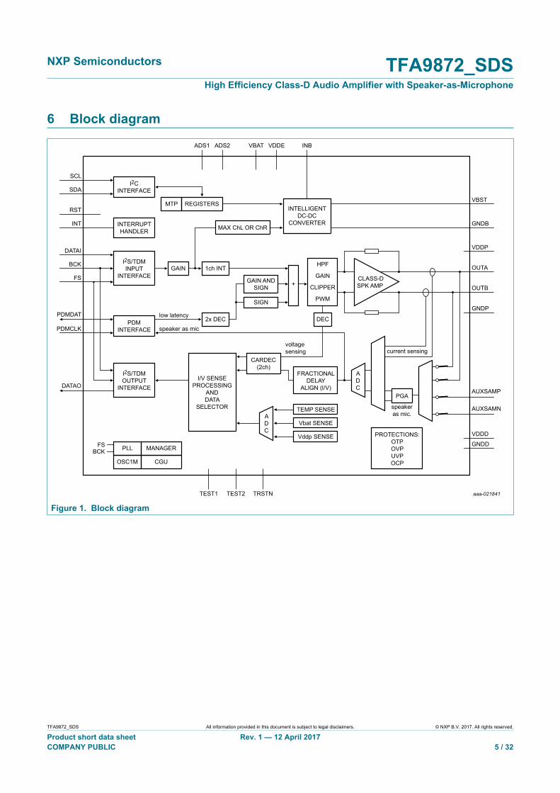
8 Functional description
The TFA9872 is a highly efficient Bridge Tied Load (BTL) class-D audio amplifierembedding Speaker-as-Microphone (SaM) support, as depicted in the block diagram ofFigure 1.
The TFA9872 contains a TDM/I2S input/output interface for communicating with the audiohost. The maximum number of slots is 16 (at fs = 48 kHz) and the minimum number is 2(I2S mode). The interface is compliant with all I2S interface configurations and supports awide range of TDM interface configurations. It also features an optional ultrasonic path tothe speaker.
The TFA9872 features a slave-configurable IN or OUT PDM interface. This audiointerface can be connected to the audio host to provide a low-latency path (for sidetone mixing) to the speaker. The 1-bit PDM stream is decimated and applied to theTDM interface. The PDM stream can, optionally, be attenuated or amplified by the gainmodule. Soft mute control prevents pop and click noise occurring when this signal path isswitched on or off. The PDM output also provides a SaM stream back to the host.
At low battery voltage levels, the gain is automatically reduced to limit battery current(when battery safeguard is enabled).
The digital audio stream is converted into two PWM signals which are then injected intothe class-D audio amplifier. The 3-level PWM scheme supports filterless speaker drive.
An adaptive DC-to-DC converter boosts the battery supply voltage when the audiostream crosses two programmable voltage thresholds. It switches automatically toFollower mode (VBST = VBAT; no boost) when the audio output voltage is lower than thebattery voltage.
The SaM feature is available in both PDM and I2S modes. This function can be used toturn the speaker into a dynamic microphone, providing an output audio stream on thedigital interfaces. Due to the nature of the speaker membrane, the microphone equivalentcharacteristics perform best in high Sound Pressure Level (SPL) environments.Consequently, this feature is targeted at specific use cases such as concert recording orcalls affected by wind noise. It is not intended to replace a primary/standard microphonebut rather to complement it in such use cases by providing a signal that is less sensitiveto saturation.
For SaM, a dedicated PGA is used to amplify the weak signal coming from the mainspeaker or receiver speaker. The result is a microphone that can handle high SPLenvironments.
SaM can be enabled on the main speaker connected to OUTA/OUTB, when the amplifieris off. Alternatively, SaM can be enabled on auxiliary inputs AUXSAMP/AUXSAMN, withthe receiver speaker connected as input.

NXP Semiconductors TFA9872_SDSHigh Efficiency Class-D Audio Amplifier with Speaker-as-Microphone
TFA9872_SDS All information provided in this document is subject to legal disclaimers. © NXP B.V. 2017. All rights reserved.
Product short data sheet Rev. 1 — 12 April 2017COMPANY PUBLIC 10 / 32
9 Limiting valuesTable 4. Limiting valuesIn accordance with the Absolute Maximum Rating System (IEC 60134).
Symbol Parameter Conditions Min Max Uniton pin VBAT -0.3 +6 V
on pins VBST, VDDP, AUXSAMP, AUXSAMN -0.3 +12 V
on pin INB, OUTA, OUTB -0.3 +12 [1] V
Vx voltage on pin x
on pins VDDD, VDDE, TEST1, TEST2 -0.3 +2.5 V
Tj junction temperature -40 +150 °C
Tstg storage temperature -55 +150 °C
Tamb ambient temperature -40 +85 °C
according to Human Body Model (HBM) -2 +2 kVVESD electrostatic discharge voltage
according to Charge Device Model (CDM) -500 +500 V
[1] Using an NXP demo board with a 1 mm wire/PCB track length on pin INB, AC pulses up to 18 V and -9 V can be observed without causing any damageas these spikes only partly penetrate the device (which is protected by internal clamp circuits).
10 Thermal characteristicsTable 5. Thermal characteristicsSymbol Parameter Conditions Typ UnitRth(j-a) thermal resistance from junction to ambient 4-layer application board 36 K/W

NXP Semiconductors TFA9872_SDSHigh Efficiency Class-D Audio Amplifier with Speaker-as-Microphone
TFA9872_SDS All information provided in this document is subject to legal disclaimers. © NXP B.V. 2017. All rights reserved.
Product short data sheet Rev. 1 — 12 April 2017COMPANY PUBLIC 11 / 32
11 Characteristics
11.1 DC Characteristics
Table 6. DC characteristicsAll parameters guaranteed for VBAT = 3.6 V; VDDD = 1.8 V; VDDP = VBST = 9.0 V; Adaptive Boost mode; LBST = 1 μH[1]; RL = 8Ω[1]; LL = 44 μH[1]; fi = 1 kHz; fs = 48 kHz; Tamb = 25 °C; default settings, unless otherwise specified.
Symbol Parameter Conditions Min Typ Max UnitVBAT battery supply voltage on pin VBAT
VBAT must not be lowerthan VDDD or VDDE in application
2.7 - 5.5 V
Active stateon pin VBAT; Operating mode with loadRL = 6 Ω; DC-to-DC in Adaptive Boostmode; Po = 380 mW, (average musicpower), VBAT = 4.0 V, VDDP = 8.5 V
- 122 - mA
Idle stateon pin VBAT; Operating mode with loadRL = 6 Ω and no output signal (idle);DC-to-DC converter in Adaptive Boostmode; VBAT = 4.0 V, VDDP = 8.5 V
- 1.8 - mA
IBAT battery supply current
Power-down stateon pin VBAT; DC-to-DC in power downmode; Tj = 25 °C, no clock.
- 1 - μA
VDDP power supply voltage on pin VDDP 2.7 - 10 V
VDD(IO) input/output supply voltage on pin VDDE 1.65 1.8 1.95 V
VDDD digital supply voltage on pin VDDD 1.65 1.8 1.95 V
Active stateon pin VDDD; Operating mode withload RL = 6 Ω; DC-to-DC in AdaptiveBoost mode; Po = 380 mW, (averagemusic power); VBAT = 4.0 V;VDDP =8.5 V
- 6.8 - mA
Idle stateon pin VDDD; Operating mode with loadRL = 6 Ω and no output signal (idle);DC-to-DC converter in Adaptive Boostmode; VBAT = 4.0 V, VDDP = 8.5 V
- 4.1 - mA
IDDD digital supply current
Power-down stateon pin VDDD; DC-to-DC in power downmode; Tj = 25 °C, no clock.
- 10 - μA
Pins FS, BCK, DATAI, ADS1, ADS2, SCL, SDA, PDMCLK, PDMDAT, RST, TRSTN
VIH HIGH-level input voltage 0.7VDDD - 3.6 V
VIL LOW-level input voltage - - 0.3VDDD V
Ci input capacitance [2] - - 3 pF

NXP Semiconductors TFA9872_SDSHigh Efficiency Class-D Audio Amplifier with Speaker-as-Microphone
TFA9872_SDS All information provided in this document is subject to legal disclaimers. © NXP B.V. 2017. All rights reserved.
Product short data sheet Rev. 1 — 12 April 2017COMPANY PUBLIC 12 / 32
Symbol Parameter Conditions Min Typ Max UnitILI input leakage current 1.8 V on input pin - - 0.1 μA
Pins DATAO, INT, PDMDAT, push-pull output stages
VOH HIGH-level output voltage IOH = 4 mA - - VDDD -0.4
V
VOL LOW-level output voltage IOL = 4 mA - - 400 mV
Pins SDA, open drain outputs, external 10 kΩ resistor to VDDD
VOH HIGH-level output voltage IOH = 4 mA - - VDDD -0.4
V
VOL LOW-level output voltage IOL = 4 mA - - 400 mV
Pins OUTA, OUTB
RDSon drain-source on-stateresistance
PMOS + NMOS transistors - 510 - mΩ
Protection
Tact(th_prot) thermal protection activationtemperature
130 - 150 °C
Vuvp(VBAT) undervoltage protectionvoltage on pin VBAT
2.3 - 2.5 V
IO(ocp) overcurrent protection outputcurrent
2 - - A
DC-to-DC converter
Vbst boost voltage DCVOS = 111; Boost mode (aftertrimming)
9.32 9.5 9.68 V
[1] LBST = boost converter inductance; RL = load resistance; LL = load inductance (speaker).[2] This parameter is not tested during production; the value is guaranteed by design and checked during product validation.

NXP Semiconductors TFA9872_SDSHigh Efficiency Class-D Audio Amplifier with Speaker-as-Microphone
TFA9872_SDS All information provided in this document is subject to legal disclaimers. © NXP B.V. 2017. All rights reserved.
Product short data sheet Rev. 1 — 12 April 2017COMPANY PUBLIC 13 / 32
11.2 AC characteristics
Table 7. AC characteristicsAll parameters guaranteed for VBAT = 3.6 V; VDDD = 1.8 V; VDDP = VBST = 9.0 V; Adaptive Boost mode; LBST = 1 μH[1]; RL =8 Ω[1]; LL = 44 μH[1]; fi = 1 kHz; fs = 48 kHz; Tamb = 25 °C; default settings, unless otherwise specified.
Symbol Parameter Conditions Min Typ Max UnitAmplifier output power
Hands-free speaker, THD+N = 1 %
RL = 8 Ω; fs = 48 kHz, VBST =9.5 V, VBAT = 4.0 V
3.6 5.1 - W
RL = 6 Ω; fs = 48 kHz, VBST =9.5 V, VBAT = 4.0 V
- 5.9 - W
RL = 4 Ω; fs = 48 kHz, VBST = 9.5V, VBAT = 4.0 V
- 6.0 - W
RL = 8 Ω; fs = 48 kHz, VBST =8.5 V, VBAT = 3.6 V
3.6 4.0 - W
RL = 6 Ω; fs = 48 kHz, VBST =8.5 V, VBAT = 3.6 V
- 5.1 - W
RL = 4 Ω; fs = 48 kHz, VBST =8.5 V, VBAT = 3.6 V
- 5.2 - W
Receiver speaker.THD+N = 1 %;VBST = 9.5 V,
RL = 32 Ω; Voice mode - 0.2 - W
Po(AV) average output power
RL = 32 Ω; Audio mode - 1.2 - W
Amplifier output pins (OUTA and OUTB)
|VO(offset)| output offset voltage absolute value after trimming; VDDP =3.4 V to 9.5 V, VBAT = 3.4 V to 5 V
- - 1.0 mV
Amplifier performances
on pin VBAT; Operating mode withload; RL = 6 Ω; DC-to-DC in AdaptiveBoost mode, Po = 380 mW, (averagemusic power), VBAT = 4.0 V, VDDP =8.5 V
[2] - 80 - %
on pin VBAT; input: 100 Hz sinewave, RL = 8 Ω; DC-to-DC inAdaptive Boost mode, VBAT = 4.0 V,VDDP = 8.5 V,Po = 700 mW
[2] - 90 - %
ηpo output power efficiency
on pin VBAT; input: 100 Hz sinewave, RL = 8 Ω; DC-to-DC inAdaptive Boost mode, VBAT = 4.0 V,VDDP = 8.5 V,Po = 4 W
[2] - 84 - %
VDDP > 9 V, Po = 2.0 W, RL = 8 Ω [2] - 0.04 0.09 %THD+N total harmonic distortion-plus-noise
VDDP > 9 V, Po = 2.0 W, RL = 4 Ω [2] - - 0.09 %
Vn(o) output noise voltage A-weighted; DATAI = 0 V; Low Noisemode (ISTLA = 1); fs = 8 kHz
[2] - 19 24 μV

NXP Semiconductors TFA9872_SDSHigh Efficiency Class-D Audio Amplifier with Speaker-as-Microphone
TFA9872_SDS All information provided in this document is subject to legal disclaimers. © NXP B.V. 2017. All rights reserved.
Product short data sheet Rev. 1 — 12 April 2017COMPANY PUBLIC 14 / 32
Symbol Parameter Conditions Min Typ Max UnitA-weighted; DATAI = 0 V; Low Noisemode (ISTLA = 1); fs = 16 kHz
[2] - 55 60 μV
S/N signal-to-noise ratio A-weighted, VBAT = 3.4 V to 5 V,maximum signal at THD = 1 %
[2] 100 - - dB
from VBAT; booster in follower mode(VDDP = VBAT); fripple = 217 Hz squarewave, Vripple = 50 mV(p-p), VBAT =4.0 V
- 80 - dB
from VBAT; booster in follower mode(VDDP = VBAT); fripple = 20 Hz to 1 kHzsine wave, Vripple = 200 mV (RMS),VBAT = 3.4 V to 5.0 V; Low Powerand Low Noise modes on
60 80 - dB
from VBAT; fripple = 20 Hz to 1 kHzsine wave, Vripple = 200 mV (RMS),VBAT = 3.4 V to 5.0 V; DC-DC infollower OR booster; Low Power andLow Noise modes off
- 75 - dB
PSRR power supply rejection ratio
from VBAT; booster in follower mode(VDDP = VBAT); fripple = 1 kHz to 20kHz sine wave, Vripple = 200 mV(RMS), VBAT = 3.4 V to 5.0 V
- 70 - dB
∆G/Δf gain variation with frequency BW = 20 Hz to 15 kHz, VBAT = 3.4 Vto 5 V
-0.1 - 0.7 dB
VPOP pop noise voltage at mode transition and gain change. 2 mV
RL load resistance 4 8 32 Ω
CL load capacitance - - 200 pF
fsw switching frequency directly coupled to the I2S inputfrequency
256 - 384 kHz
Gv voltage gain I2S/TDM to VO; INPLEV = 0 (0 dB) 6 - 21 dB
Amplifier power-up, power-down and propagation delays
td(on)PLL PLL turn-on delay time PLL locked on BCK, fs = 48 kHz - 2 - ms
td(on)amp amplifier turn-on delay time fs = 48 kHz - 1 - ms
td(off) turn-off delay time - 32 - μs
td(alarm) alarm delay time - 200 - ms
fs = 16 kHz (I2S/TDM) - 1750 - μs
fs = 48 kHz (I2S/TDM) - 600 - μs
fs = 96/192 kHz (I2S/TDM) - 320 - μs
tPD propagation delay
fs = 48 kHz (PDM) - 70 - μs
Booster Inductance
Lbst boost inductance 0.7 1.0 2.2 μH
Current-sensing performance
LL(spk) speaker load inductance 30 - - μH
NXP Semiconductors TFA9872_SDSHigh Efficiency Class-D Audio Amplifier with Speaker-as-Microphone
TFA9872_SDS All information provided in this document is subject to legal disclaimers. © NXP B.V. 2017. All rights reserved.
Product short data sheet Rev. 1 — 12 April 2017COMPANY PUBLIC 15 / 32
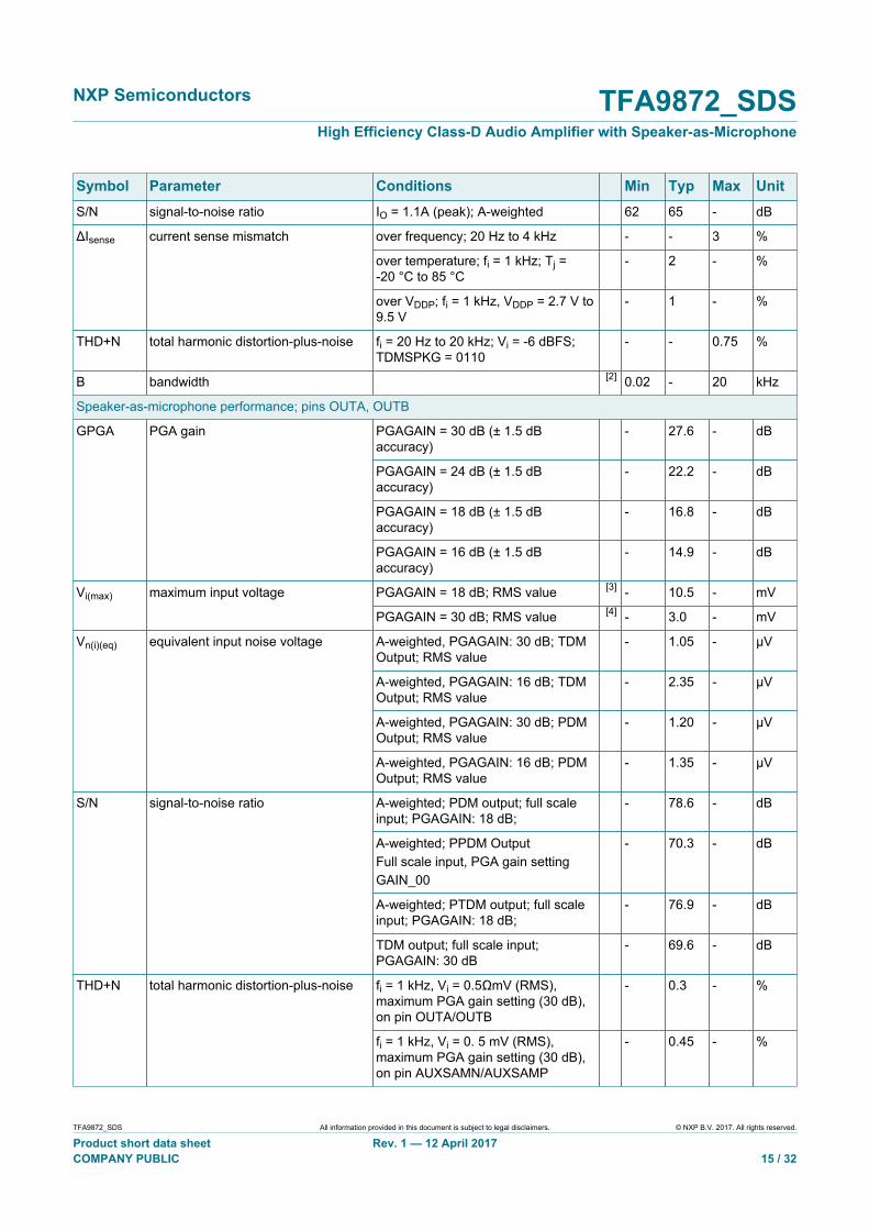
Symbol Parameter Conditions Min Typ Max UnitS/N signal-to-noise ratio IO = 1.1A (peak); A-weighted 62 65 - dB
over frequency; 20 Hz to 4 kHz - - 3 %
over temperature; fi = 1 kHz; Tj =-20 °C to 85 °C
- 2 - %
ΔIsense current sense mismatch
over VDDP; fi = 1 kHz, VDDP = 2.7 V to9.5 V
- 1 - %
THD+N total harmonic distortion-plus-noise fi = 20 Hz to 20 kHz; Vi = -6 dBFS;TDMSPKG = 0110
- - 0.75 %
B bandwidth [2] 0.02 - 20 kHz
Speaker-as-microphone performance; pins OUTA, OUTB
PGAGAIN = 30 dB (± 1.5 dBaccuracy)
- 27.6 - dB
PGAGAIN = 24 dB (± 1.5 dBaccuracy)
- 22.2 - dB
PGAGAIN = 18 dB (± 1.5 dBaccuracy)
- 16.8 - dB
GPGA PGA gain
PGAGAIN = 16 dB (± 1.5 dBaccuracy)
- 14.9 - dB
PGAGAIN = 18 dB; RMS value [3] - 10.5 - mVVi(max) maximum input voltage
PGAGAIN = 30 dB; RMS value [4] - 3.0 - mV
A-weighted, PGAGAIN: 30 dB; TDMOutput; RMS value
- 1.05 - μV
A-weighted, PGAGAIN: 16 dB; TDMOutput; RMS value
- 2.35 - μV
A-weighted, PGAGAIN: 30 dB; PDMOutput; RMS value
- 1.20 - μV
Vn(i)(eq) equivalent input noise voltage
A-weighted, PGAGAIN: 16 dB; PDMOutput; RMS value
- 1.35 - μV
A-weighted; PDM output; full scaleinput; PGAGAIN: 18 dB;
- 78.6 - dB
A-weighted; PPDM OutputFull scale input, PGA gain settingGAIN_00
- 70.3 - dB
A-weighted; PTDM output; full scaleinput; PGAGAIN: 18 dB;
- 76.9 - dB
S/N signal-to-noise ratio
TDM output; full scale input;PGAGAIN: 30 dB
- 69.6 - dB
fi = 1 kHz, Vi = 0.5ΩmV (RMS),maximum PGA gain setting (30 dB),on pin OUTA/OUTB
- 0.3 - %THD+N total harmonic distortion-plus-noise
fi = 1 kHz, Vi = 0. 5 mV (RMS),maximum PGA gain setting (30 dB),on pin AUXSAMN/AUXSAMP
- 0.45 - %
NXP Semiconductors TFA9872_SDSHigh Efficiency Class-D Audio Amplifier with Speaker-as-Microphone
TFA9872_SDS All information provided in this document is subject to legal disclaimers. © NXP B.V. 2017. All rights reserved.
Product short data sheet Rev. 1 — 12 April 2017COMPANY PUBLIC 16 / 32
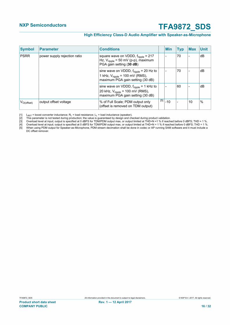
Symbol Parameter Conditions Min Typ Max Unitsquare wave on VDDD, fripple = 217Hz, Vripple = 50 mV (p-p), maximumPGA gain setting (30 dB)
- 70 - dB
sine wave on VDDD, fripple = 20 Hz to1 kHz, Vripple = 100 mV (RMS),maximum PGA gain setting (30 dB)
- 70 - dB
PSRR power supply rejection ratio
sine wave on VDDD, fripple = 1 kHz to20 kHz, Vripple = 100 mV (RMS),maximum PGA gain setting (30 dB)
- 60 - dB
VO(offset) output offset voltage % of Full Scale; PDM output only(offset is removed on TDM output)
[5] -10 - 10 %
[1] LBST = boost converter inductance; RL = load resistance; LL = load inductance (speaker).[2] This parameter is not tested during production; the value is guaranteed by design and checked during product validation.[3] Overload level at input; output is specified at 0 dBFS for TDM/PDM output max, or output limited at THD+N =1 % if reached before 0 dBFS; THD = 1 %.[4] Overload level at input; output is specified at 0 dBFS for TDM/PDM output max, or output limited at THD+N = 1 % if reached before 0 dBFS; THD = 1 %.[5] When using PDM output for Speaker-as-Microphone, PDM stream decimation shall be done in codec or AP running SAM software and it must include a
DC offset remover.

NXP Semiconductors TFA9872_SDSHigh Efficiency Class-D Audio Amplifier with Speaker-as-Microphone
TFA9872_SDS All information provided in this document is subject to legal disclaimers. © NXP B.V. 2017. All rights reserved.
Product short data sheet Rev. 1 — 12 April 2017COMPANY PUBLIC 17 / 32
11.3 I2S timing characteristics
Table 8. I2S bus interface characteristics; see Figure 4All parameters are guaranteed for VBAT = 3.6 V; VDDD = 1.8 V; VDDP = VBST = 9.0 V, Adaptive Boost mode; LBST = 1 μH[1];RL= 8 Ω[1]; LL = 44 μH[1]; fi = 1 kHz; fs = 48 kHz; Tamb = 25 °C; default settings, unless otherwise specified.
Symbol Parameter Conditions Min Typ Max Unitfs sampling frequency on pin WS, audio mode [2] 16 - 48 kHz
on pin WS, ultrasonic mode 96 - 192 kHz
fclk clock frequency on pin BCK, audio mode [2] 32fs - 384fs kHz
on pin BCK, ultrasonic mode - - 96fs MHz
WS edge to BCK HIGH [3] 10 - - nstsu set-up time
DATA edge to BCK HIGH 10 - - ns
BCK HIGH to WS edge [3] 10 - - nsth hold time
BCK HIGH to DATA edge 10 - - ns
[1] LBST = boost converter inductance; RL = load resistance; LL = load inductance.[2] The I2S bit clock input (BCK) is used as a clock input for the amplifier and the DC-to-DC converter. Note that both the BCK and WS signals must be
present for the clock to operate correctly.[3] This parameter is not tested during production; the value is guaranteed by design and checked during product validation.
BCK
FS
DATA
th tsu
010aaa750
Figure 4. I2S timing

NXP Semiconductors TFA9872_SDSHigh Efficiency Class-D Audio Amplifier with Speaker-as-Microphone
TFA9872_SDS All information provided in this document is subject to legal disclaimers. © NXP B.V. 2017. All rights reserved.
Product short data sheet Rev. 1 — 12 April 2017COMPANY PUBLIC 18 / 32
11.4 I2C timing characteristics
Table 9. I2C-bus interface characteristics; see Figure 5All parameters are guaranteed for VBAT = 3.6 V; VDDD = 1.8 V; VDDP = VBST = 9.0 V, Adaptive Boost mode; LBST = 1 μH[1];RL= 8 Ω[1]; LL = 44 μH[1]; fi = 1 kHz; fs = 48 kHz; Tamb = 25 °C; default settings, unless otherwise specified.
Symbol Parameter Conditions Min Typ Max UnitfSCL SCL clock frequency - - 400 kHz
tLOW LOW period of the SCL clock 1.3 - - μs
tHIGH HIGH period of the SCL clock 0.6 - - μs
tr rise time SDA and SCL signals [2] 20 + 0.1 Cb - - ns
tf fall time SDA and SCL signals [2] 20 + 0.1 Cb - - ns
tHD;STA hold time (repeated) START condition [3] 0.6 - - μs
tSU;STA set-up time for a repeated START condition 0.6 - - μs
tSU;STO set-up time for STOP condition 0.6 - - μs
tBUF bus free time between a STOP and STARTcondition
1.3 - - μs
tSU;DAT data set-up time 100 - - ns
tHD;DAT data hold time 0 - - μs
tSP pulse width of spikes that must besuppressed by the input filter
[4] 0 - 50 ns
Cb capacitive load for each bus line - - 400 pF
[1] LBST = boost converter inductance; RL = load resistance; LL = load inductance.[2] Cb is the total capacitance of one bus line in pF. The maximum capacitive load for each bus line is 400 pF.[3] After this period, the first clock pulse is generated.[4] To be suppressed by the input filter.
tBUFtLOW tr tf
tHD;STAtSU;STAtHD;DAT tHIGH tSU;DAT
tHD;STA
tSU;STO
tSP
P S Sr P
SDA
SCL
010aaa225
Figure 5. I2C timing

NXP Semiconductors TFA9872_SDSHigh Efficiency Class-D Audio Amplifier with Speaker-as-Microphone
TFA9872_SDS All information provided in this document is subject to legal disclaimers. © NXP B.V. 2017. All rights reserved.
Product short data sheet Rev. 1 — 12 April 2017COMPANY PUBLIC 19 / 32
11.5 PDM timing characteristics
Table 10. PDM interface characteristics; see Figure 6All parameters are guaranteed for VBAT = 3.6 V; VDDD = 1.8 V; VDDP = VBST = 9.0 V, Adaptive Boost mode; LBST = 1 μH[1];RL= 8 Ω[1]; LL = 44 μH[1]; fi = 1 kHz; fs = 48 kHz; Tamb = 25 °C; default settings, unless otherwise specified.
Symbol Parameter Conditions Min Typ Max Unitfclk clock frequency - 3.072 [2] - MHz
δclk clock duty cycle 45 - 55 %
after clock HIGH 30 - - nsth hold time
after clock LOW 30 - - ns
after clock HIGH 30 - - nstsu set-up time
after clock LOW 30 - - ns
[1] LBST = boost converter inductance; RL = load resistance; LL = load inductance.[2] PDM Clock is 64xfs, with fs selected by AUDFS. Typical 3.072 Mhz is corresponding to fs = 48 kHz.
tsu(CLKH)
th(CLKH)
tsu(CLKL)
th(CLKL)
CLK
DATA
010aaa711
Figure 6. PDM timing

NXP Semiconductors TFA9872_SDSHigh Efficiency Class-D Audio Amplifier with Speaker-as-Microphone
TFA9872_SDS All information provided in this document is subject to legal disclaimers. © NXP B.V. 2017. All rights reserved.
Product short data sheet Rev. 1 — 12 April 2017COMPANY PUBLIC 20 / 32
12 Application information
12.1 Application diagrams
l2C
SPKl2S
+
-speaker
SDACTRL (I2C)
AUDIO IN (TDM)
SPKBST (TDM)OUTA
OUTBA
UX
SA
MP
TRST
N
AU
XS
AM
N
TES
T2
GN
DD
GN
DP
GN
DB
AD
S2
AD
S1
SCL
DATAIN
FS
BCK
DATAO
RST
INT
BASEBANDPROCESSOR
TFA9872
PDMCLK
PDMDAT
aaa-021842
TES
T1
CVDDP33 µFVBST
VDDP
1.8 V
CVDDD100 nF
VD
DD
/V
DD
E
1 µH
VB
AT
INB
1 nF22 µFCVBAT
LBST
CBST
RFVBAT5.1 Ω
1 µFCFVBAT
Figure 7. Typical mono application

NXP Semiconductors TFA9872_SDSHigh Efficiency Class-D Audio Amplifier with Speaker-as-Microphone
TFA9872_SDS All information provided in this document is subject to legal disclaimers. © NXP B.V. 2017. All rights reserved.
Product short data sheet Rev. 1 — 12 April 2017COMPANY PUBLIC 21 / 32
l2C
SPKl2S
SDACTRL (I2C)
AUDIO IN (TDM)
SPKBST (TDM)
SCL
DATAIN
FS
BCK
DATAO
RST
INT
BASEBANDPROCESSOR
TFA9872
PDMCLK
PDMDAT
SDA
ADS
1
SCL
DATAIN
FS
BCK
DATAO
RST
INT
1.8 V
TFA9872
PDMCLK
PDMDAT
aaa-021843
1.8 V
CVDDD100 nF
VD
DD
/V
DD
E
1 µH
VBA
T
INB 1 nF22 µF
CVBAT
LBST
CBST
RFVBAT5.1 Ω
1 µFCFVBAT
1.8 V
CVDDD100 nF
VD
DD
/V
DD
E
1 µH
VB
AT
INB
1 nF22 µFCVBAT
LBST
CBST
RFVBAT5.1 Ω
1 µFCFVBAT
AU
XS
AM
P
TRS
TN
AU
XS
AM
N
TES
T2
GN
DD
GN
DP
GN
DB
AD
S2
TES
T1
AU
XS
AM
P
TRS
TN
AU
XS
AM
N
TES
T2
GN
DD
GN
DP
GN
DB
AD
S2
AD
S1
TES
T1
+
-speaker
OUTA
OUTB
CVDDP33 µFVBST
VDDP
+
-speaker
OUTA
OUTB
CVDDP33 µFVBST
VDDP
Figure 8. Typical stereo application (using separated coils)

NXP Semiconductors TFA9872_SDSHigh Efficiency Class-D Audio Amplifier with Speaker-as-Microphone
TFA9872_SDS All information provided in this document is subject to legal disclaimers. © NXP B.V. 2017. All rights reserved.
Product short data sheet Rev. 1 — 12 April 2017COMPANY PUBLIC 22 / 32
l2C
SPKl2S
SDACTRL (I2C)
AUDIO IN (TDM)
SPKBST (TDM)
SCL
DATAIN
FS
BCK
DATAO
RST
INT
BASEBANDPROCESSOR
TFA9872
PDMCLK
PDMDAT
SDA
ADS
1
SCL
DATAIN
FS
BCK
DATAO
RST
INT
1.8 V
TFA9872
PDMCLK
PDMDAT
aaa-026445
1.8 V
CVDDD100 nF
VDD
D/
VDD
E
1 µH
VBAT
INB 1 nF22 µF
CVBAT
LBST
CBST
RFVBAT5.1 Ω
1 µFCFVBAT
1.8 V
CVDDD100 nF
VDD
D/
VDD
E
VBA
T
INB
RFVBAT5.1 Ω
1 µFCFVBAT
AUX
SAM
P
TRS
TN
AU
XSAM
N
TES
T2
GN
DD
GN
DP
GN
DB
ADS2
TEST
1
AUX
SAM
P
TRS
TN
AU
XSA
MN
TEST
2
GN
DD
GN
DP
GN
DB
ADS
2
ADS
1
TEST
1
+
-speaker
OUTA
OUTB
CVDDP33 µFVBST
+
-speaker
OUTA
OUTB
CVDDP33 µFVBST
VDDP
VDDP
RHVBAT1 MΩ
Figure 9. Typical stereo application (using a single coil)

NXP Semiconductors TFA9872_SDSHigh Efficiency Class-D Audio Amplifier with Speaker-as-Microphone
TFA9872_SDS All information provided in this document is subject to legal disclaimers. © NXP B.V. 2017. All rights reserved.
Product short data sheet Rev. 1 — 12 April 2017COMPANY PUBLIC 23 / 32
+
-speaker
SDACTRL (I2C)
AUDIO IN (TDM)
SPKBST (TDM)
OUTA
OUTB
SCL
DATAIN
FS
BCK
DATAO
RST
INT
TFA9872
aaa-021844
CVDDP33 µFVBST
VDDP
1.8 V
CVDDD100 nF
VD
DD
/V
DD
E
1 µH
VBA
T
INB
1 nF22 µFCVBAT
LBST
CBST
RFVBAT5.1 Ω
1 µFCFVBAT
l2C
SPKl2S
BASEBANDPROCESSOR
PDM SaM (PDM)
PDMCLK
PDMDAT
TES
T2
TRS
TN
TES
T1
GN
DD
GN
DP
GN
DB
ADS2
ADS1
AUXSAMN
AUXSAMP
FAUX1
FAUX2
+
-speaker
100 pFCAUX1
CAUX2 100 pF33 nFCAUX3
RAUX1
RAUX2
The configuration shown also supports speaker playbackFigure 10. Typical SaM application

NXP Semiconductors TFA9872_SDSHigh Efficiency Class-D Audio Amplifier with Speaker-as-Microphone
TFA9872_SDS All information provided in this document is subject to legal disclaimers. © NXP B.V. 2017. All rights reserved.
Product short data sheet Rev. 1 — 12 April 2017COMPANY PUBLIC 24 / 32
13 Package outline
ReferencesOutlineversion
Europeanprojection Issue date
IEC JEDEC JEITA
SOT1459-2 - - -
sot1459-2_po
16-02-2516-03-01
Unit
mmmaxnommin
0.29 3.16 2.492.4 0.05 0.03
A
Dimensions (mm are the original dimensions)
WLCSP42: wafer level chip-scale package; 42 bumps; 3.13 x 2.46 x 0.50 mm SOT1459-2
A1 A2
0.325
0.2750.26 3.13 2.46 0.4
b D E e e1
2.0
e2 v w
0.020.23 3.10 2.43
0.365 0.365 0.215
ZD1 ZD2 ZE2
0.245
ZE1 y
0.3000.23
0.170.20
0.54
0.460.50
0
scale
3 mm
detail X
X
C
y
654321
e2
A
ball A1index area
ball A1index area
BE A
DA
A2
A1
bAC BØ v
CØ w
e1
e
e
ZD2
ZE2ZE1
ZD1
B
C
D
E
F
G
Figure 11. Package outline TFA9872AUK/N1 (WLSCP42)

NXP Semiconductors TFA9872_SDSHigh Efficiency Class-D Audio Amplifier with Speaker-as-Microphone
TFA9872_SDS All information provided in this document is subject to legal disclaimers. © NXP B.V. 2017. All rights reserved.
Product short data sheet Rev. 1 — 12 April 2017COMPANY PUBLIC 25 / 32
ReferencesOutlineversion
Europeanprojection Issue date
IEC JEDEC JEITA
SOT1459-3 - - -
sot1459-3_po
16-03-0116-05-09
Unit
mmmaxnommin
3.16 2.492.4 0.05 0.03
A
Dimensions (mm are the original dimensions)
WLCSP42: wafer level chip-scale package; 42 bumps; 3.13 x 2.46 x 0.525 mm (backside coating included) SOT1459-3
A1 A2
0.26 3.13 2.46 0.4
b D E e e1
2.0
e2 v w
0.023.10 2.43
0.365 0.365 0.215
ZD1 ZD2 ZE2
0.245
ZE1 y
0.330.200.565
0.4850.525
0
scale
3 mm
detail X
X
C
y
654321
e2
A
ball A1index area
ball A1index area
BE A
DA
A2
A1
bAC BØ v
CØ w
e1
e
e
ZD2
ZE2ZE1
ZD1
B
C
D
E
F
G
Note: Backside coating 25 µm
Figure 12. Package outline TFA9872CUK/N1 (WLCSP42)

NXP Semiconductors TFA9872_SDSHigh Efficiency Class-D Audio Amplifier with Speaker-as-Microphone
TFA9872_SDS All information provided in this document is subject to legal disclaimers. © NXP B.V. 2017. All rights reserved.
Product short data sheet Rev. 1 — 12 April 2017COMPANY PUBLIC 26 / 32
14 Soldering of WLCSP packages
14.1 Introduction to soldering WLCSP packagesThis text provides a very brief insight into a complex technology. A more in-depth accountof soldering WLCSP (Wafer Level Chip-Size Packages) can be found in application noteAN10439 “Wafer Level Chip Scale Package” and in application note AN10365 “Surfacemount reflow soldering description”.
Wave soldering is not suitable for this package.
All NXP WLCSP packages are lead-free.
14.2 Board mountingBoard mounting of a WLCSP requires several steps:
1. Solder paste printing on the PCB2. Component placement with a pick and place machine3. The reflow soldering itself
14.3 Reflow solderingKey characteristics in reflow soldering are:
• Lead-free versus SnPb soldering; note that a lead-free reflow process usually leads tohigher minimum peak temperatures (see Figure 1) than a SnPb process, thus reducingthe process window
• Solder paste printing issues, such as smearing, release, and adjusting the processwindow for a mix of large and small components on one board
• Reflow temperature profile; this profile includes preheat, reflow (in which the boardis heated to the peak temperature), and cooling down. It is imperative that the peaktemperature is high enough for the solder to make reliable solder joints (a solderpaste characteristic) while being low enough that the packages and/or boards are notdamaged. The peak temperature of the package depends on package thickness andvolume and is classified in accordance with Table 11.
Table 11. Lead-free process (from J-STD-020D)Package reflow temperature (°C)
Volume (mm3)
Package thickness (mm)
< 350 350 to 2000 > 2000< 1.6 260 260 260
1.6 to 1.5 260 250 245
> 2.5 250 245 245
Moisture sensitivity precautions, as indicated on the packing, must be respected at alltimes.
Studies have shown that small packages reach higher temperatures during reflowsoldering, see Figure 13.

NXP Semiconductors TFA9872_SDSHigh Efficiency Class-D Audio Amplifier with Speaker-as-Microphone
TFA9872_SDS All information provided in this document is subject to legal disclaimers. © NXP B.V. 2017. All rights reserved.
Product short data sheet Rev. 1 — 12 April 2017COMPANY PUBLIC 27 / 32
001aac844
temperature
time
minimum peak temperature= minimum soldering temperature
maximum peak temperature= MSL limit, damage level
peaktemperature
MSL: Moisture Sensitivity LevelFigure 13. Temperature profiles for large and small components
For further information on temperature profiles, refer to application note AN10365“Surface mount reflow soldering description”.
14.3.1 Stand offThe stand off between the substrate and the chip is determined by:
• The amount of printed solder on the substrate• The size of the solder land on the substrate• The bump height on the chip
The higher the stand off, the better the stresses are released due to TEC (ThermalExpansion Coefficient) differences between substrate and chip.
The higher the stand off, the better the stresses are released due to TEC (ThermalExpansion Coefficient) differences between substrate and chip.
14.3.2 Quality of solder jointA flip-chip joint is considered to be a good joint when the entire solder land has beenwetted by the solder from the bump. The surface of the joint should be smooth andthe shape symmetrical. The soldered joints on a chip should be uniform. Voids in thebumps after reflow can occur during the reflow process in bumps with high ratio of bumpdiameter to bump height, i.e. low bumps with large diameter. No failures have been foundto be related to these voids. Solder joint inspection after reflow can be done with X-ray tomonitor defects such as bridging, open circuits and voids.
14.3.3 ReworkIn general, rework is not recommended. By rework we mean the process of removingthe chip from the substrate and replacing it with a new chip. If a chip is removed from thesubstrate, most solder balls of the chip will be damaged. In that case it is recommendednot to re-use the chip again.

NXP Semiconductors TFA9872_SDSHigh Efficiency Class-D Audio Amplifier with Speaker-as-Microphone
TFA9872_SDS All information provided in this document is subject to legal disclaimers. © NXP B.V. 2017. All rights reserved.
Product short data sheet Rev. 1 — 12 April 2017COMPANY PUBLIC 28 / 32
Device removal can be done when the substrate is heated until it is certain that all solderjoints are molten. The chip can then be carefully removed from the substrate withoutdamaging the tracks and solder lands on the substrate. Removing the device mustbe done using plastic tweezers, because metal tweezers can damage the silicon. Thesurface of the substrate should be carefully cleaned and all solder and flux residues and/or underfill removed. When a new chip is placed on the substrate, use the flux processinstead of solder on the solder lands. Apply flux on the bumps at the chip side as wellas on the solder pads on the substrate. Place and align the new chip while viewing witha microscope. To reflow the solder, use the solder profile shown in application noteAN10365 “Surface mount reflow soldering description”.
14.3.4 CleaningCleaning can be done after reflow soldering.
NXP Semiconductors TFA9872_SDSHigh Efficiency Class-D Audio Amplifier with Speaker-as-Microphone
TFA9872_SDS All information provided in this document is subject to legal disclaimers. © NXP B.V. 2017. All rights reserved.
Product short data sheet Rev. 1 — 12 April 2017COMPANY PUBLIC 29 / 32
15 Revision historyTable 12. Revision historyDocument ID Release date Data sheet status Change notice SupersedesTFA9872_SDS v.1 20170412 Product data sheet - -

NXP Semiconductors TFA9872_SDSHigh Efficiency Class-D Audio Amplifier with Speaker-as-Microphone
TFA9872_SDS All information provided in this document is subject to legal disclaimers. © NXP B.V. 2017. All rights reserved.
Product short data sheet Rev. 1 — 12 April 2017COMPANY PUBLIC 30 / 32
16 Legal information
16.1 Data sheet status
Document status[1][2] Product status[3] Definition
Objective [short] data sheet Development This document contains data from the objective specification for productdevelopment.
Preliminary [short] data sheet Qualification This document contains data from the preliminary specification.
Product [short] data sheet Production This document contains the product specification.
[1] Please consult the most recently issued document before initiating or completing a design.[2] The term 'short data sheet' is explained in section "Definitions".[3] The product status of device(s) described in this document may have changed since this document was published and may differ in case of multiple
devices. The latest product status information is available on the Internet at URL http://www.nxp.com.
16.2 DefinitionsDraft — The document is a draft version only. The content is still underinternal review and subject to formal approval, which may result inmodifications or additions. NXP Semiconductors does not give anyrepresentations or warranties as to the accuracy or completeness ofinformation included herein and shall have no liability for the consequencesof use of such information.
Short data sheet — A short data sheet is an extract from a full data sheetwith the same product type number(s) and title. A short data sheet isintended for quick reference only and should not be relied upon to containdetailed and full information. For detailed and full information see therelevant full data sheet, which is available on request via the local NXPSemiconductors sales office. In case of any inconsistency or conflict with theshort data sheet, the full data sheet shall prevail.
Product specification — The information and data provided in a Productdata sheet shall define the specification of the product as agreed betweenNXP Semiconductors and its customer, unless NXP Semiconductors andcustomer have explicitly agreed otherwise in writing. In no event however,shall an agreement be valid in which the NXP Semiconductors productis deemed to offer functions and qualities beyond those described in theProduct data sheet.
16.3 DisclaimersLimited warranty and liability — Information in this document is believedto be accurate and reliable. However, NXP Semiconductors does notgive any representations or warranties, expressed or implied, as to theaccuracy or completeness of such information and shall have no liabilityfor the consequences of use of such information. NXP Semiconductorstakes no responsibility for the content in this document if provided by aninformation source outside of NXP Semiconductors. In no event shall NXPSemiconductors be liable for any indirect, incidental, punitive, special orconsequential damages (including - without limitation - lost profits, lostsavings, business interruption, costs related to the removal or replacementof any products or rework charges) whether or not such damages are basedon tort (including negligence), warranty, breach of contract or any otherlegal theory. Notwithstanding any damages that customer might incur forany reason whatsoever, NXP Semiconductors’ aggregate and cumulativeliability towards customer for the products described herein shall be limitedin accordance with the Terms and conditions of commercial sale of NXPSemiconductors.
Right to make changes — NXP Semiconductors reserves the right tomake changes to information published in this document, including withoutlimitation specifications and product descriptions, at any time and withoutnotice. This document supersedes and replaces all information supplied priorto the publication hereof.
Suitability for use — NXP Semiconductors products are not designed,authorized or warranted to be suitable for use in life support, life-critical orsafety-critical systems or equipment, nor in applications where failure ormalfunction of an NXP Semiconductors product can reasonably be expectedto result in personal injury, death or severe property or environmentaldamage. NXP Semiconductors and its suppliers accept no liability forinclusion and/or use of NXP Semiconductors products in such equipment orapplications and therefore such inclusion and/or use is at the customer’s ownrisk.
Applications — Applications that are described herein for any of theseproducts are for illustrative purposes only. NXP Semiconductors makesno representation or warranty that such applications will be suitablefor the specified use without further testing or modification. Customersare responsible for the design and operation of their applications andproducts using NXP Semiconductors products, and NXP Semiconductorsaccepts no liability for any assistance with applications or customer productdesign. It is customer’s sole responsibility to determine whether the NXPSemiconductors product is suitable and fit for the customer’s applicationsand products planned, as well as for the planned application and use ofcustomer’s third party customer(s). Customers should provide appropriatedesign and operating safeguards to minimize the risks associated withtheir applications and products. NXP Semiconductors does not accept anyliability related to any default, damage, costs or problem which is basedon any weakness or default in the customer’s applications or products, orthe application or use by customer’s third party customer(s). Customer isresponsible for doing all necessary testing for the customer’s applicationsand products using NXP Semiconductors products in order to avoid adefault of the applications and the products or of the application or use bycustomer’s third party customer(s). NXP does not accept any liability in thisrespect.
Limiting values — Stress above one or more limiting values (as defined inthe Absolute Maximum Ratings System of IEC 60134) will cause permanentdamage to the device. Limiting values are stress ratings only and (proper)operation of the device at these or any other conditions above thosegiven in the Recommended operating conditions section (if present) or theCharacteristics sections of this document is not warranted. Constant orrepeated exposure to limiting values will permanently and irreversibly affectthe quality and reliability of the device.
Terms and conditions of commercial sale — NXP Semiconductorsproducts are sold subject to the general terms and conditions of commercialsale, as published at http://www.nxp.com/profile/terms, unless otherwiseagreed in a valid written individual agreement. In case an individualagreement is concluded only the terms and conditions of the respectiveagreement shall apply. NXP Semiconductors hereby expressly objects toapplying the customer’s general terms and conditions with regard to thepurchase of NXP Semiconductors products by customer.
No offer to sell or license — Nothing in this document may be interpretedor construed as an offer to sell products that is open for acceptance orthe grant, conveyance or implication of any license under any copyrights,patents or other industrial or intellectual property rights.

NXP Semiconductors TFA9872_SDSHigh Efficiency Class-D Audio Amplifier with Speaker-as-Microphone
TFA9872_SDS All information provided in this document is subject to legal disclaimers. © NXP B.V. 2017. All rights reserved.
Product short data sheet Rev. 1 — 12 April 2017COMPANY PUBLIC 31 / 32
Quick reference data — The Quick reference data is an extract of theproduct data given in the Limiting values and Characteristics sections of thisdocument, and as such is not complete, exhaustive or legally binding.
Export control — This document as well as the item(s) described hereinmay be subject to export control regulations. Export might require a priorauthorization from competent authorities.
Non-automotive qualified products — Unless this data sheet expresslystates that this specific NXP Semiconductors product is automotive qualified,the product is not suitable for automotive use. It is neither qualified nortested in accordance with automotive testing or application requirements.NXP Semiconductors accepts no liability for inclusion and/or use of non-automotive qualified products in automotive equipment or applications. Inthe event that customer uses the product for design-in and use in automotiveapplications to automotive specifications and standards, customer (a) shalluse the product without NXP Semiconductors’ warranty of the product for
such automotive applications, use and specifications, and (b) whenevercustomer uses the product for automotive applications beyond NXPSemiconductors’ specifications such use shall be solely at customer’s ownrisk, and (c) customer fully indemnifies NXP Semiconductors for any liability,damages or failed product claims resulting from customer design and useof the product for automotive applications beyond NXP Semiconductors’standard warranty and NXP Semiconductors’ product specifications.
Translations — A non-English (translated) version of a document is forreference only. The English version shall prevail in case of any discrepancybetween the translated and English versions.
16.4 TrademarksNotice: All referenced brands, product names, service names andtrademarks are the property of their respective owners.

NXP Semiconductors TFA9872_SDSHigh Efficiency Class-D Audio Amplifier with Speaker-as-Microphone
Please be aware that important notices concerning this document and the product(s)described herein, have been included in section 'Legal information'.
© NXP B.V. 2017. All rights reserved.For more information, please visit: http://www.nxp.comFor sales office addresses, please send an email to: [email protected]
Date of release: 12 April 2017Document identifier: TFA9872_SDS
Contents1 General description ............................................ 12 Features and benefits .........................................23 Applications .........................................................24 Quick reference data .......................................... 35 Ordering information .......................................... 46 Block diagram ..................................................... 57 Pinning information ............................................ 67.1 Pinning ...............................................................67.2 Pin description ................................................... 78 Functional description ........................................99 Limiting values ..................................................1010 Thermal characteristics ....................................1011 Characteristics .................................................. 1111.1 DC Characteristics ...........................................1111.2 AC characteristics ............................................1311.3 I2S timing characteristics .................................1711.4 I2C timing characteristics ................................ 1811.5 PDM timing characteristics .............................. 1912 Application information ....................................2012.1 Application diagrams ....................................... 2013 Package outline .................................................2414 Soldering of WLCSP packages ........................2614.1 Introduction to soldering WLCSP packages .....2614.2 Board mounting ............................................... 2614.3 Reflow soldering .............................................. 2614.3.1 Stand off .......................................................... 2714.3.2 Quality of solder joint .......................................2714.3.3 Rework .............................................................2714.3.4 Cleaning ...........................................................2815 Revision history ................................................ 2916 Legal information ..............................................30


![Integrated AV Amplifier - pdf.crse.compdf.crse.com/manuals/3856168111.pdf · 6EN Getting Started Hookups Front speakers Front speaker (R) Front speaker (L) Amplifier} ] FRONT SPEAKERS](https://static.fdocuments.net/doc/165x107/5b15a6767f8b9a332f8d45d5/integrated-av-amplifier-pdfcrse-6en-getting-started-hookups-front-speakers.jpg)


