High-efficiency broad-bandwidth sub-wavelength … · High-efficiency broad-bandwidth...
17
1 High-efficiency broad-bandwidth sub-wavelength grating based fibre- chip coupler in SOI Siddharth Nambiar a , Shankar K Selvaraja* a a Center for Nanoscience and Engineering (CeNSE), Indian Institute of Science (IISc), Bengaluru, India, 560012 Abstract. We report a comprehensive study on the performance of uniform and non-uniform based subwavelength grating couplers in Silicon-on-Insulator. The two performance metrics, coupling efficiency and bandwidth enhancement and trade-offs is presented. We also present, design parameters to achieve high-efficiency and broadband operation based on the detailed study of various loss mechanisms in the grating. Based on the detailed analysis subwavlength grating coupler designs with efficiency as high as 84 % with a 1 dB bandwidth of 50 nm and 98 % with a 44 nm 1 dB bandwidth is presented. Keywords: Silicon Photonics, Grating coupler, Photonic integrated circuit, SOI. * [email protected] 1 Introduction One of the critical issues in integrated photonic circuits in silicon-on-insulator (SOI) platform is the ability to efficiently couple broadband light between a single-mode optical fiber (SMF) and the Si photonic wire waveguide. Edge- or butt-coupling using sophisticated mode converters have been proposed and demonstrated with high-coupling efficiency (<1 dB) and broadband operation [1– 3]. Such solutions are, however, demanding cumbersome processing steps and are not compatible with CMOS integration scheme. Alternatively, out-of-plane coupling using diffraction gratings is an elegant and versatile technique for coupling light between a sub-micron waveguide and a SMF [4, 5]. Even though grating coupler is simple in operation and implementation, the coupling efficiency and bandwidth of operation are limited. The coupling efficiency can be improved by either increasing its directionality to the optical fiber and/or by improving the modal overlap between the fiber and the diffracting grating [6]. On the other hand, improving bandwidth is not
Transcript of High-efficiency broad-bandwidth sub-wavelength … · High-efficiency broad-bandwidth...

1
High-efficiency broad-bandwidth sub-wavelength grating based fibre-chip coupler in SOI
Siddharth Nambiara, Shankar K Selvaraja*a aCenter for Nanoscience and Engineering (CeNSE), Indian Institute of Science (IISc), Bengaluru, India, 560012
Abstract. We report a comprehensive study on the performance of uniform and non-uniform based subwavelength
grating couplers in Silicon-on-Insulator. The two performance metrics, coupling efficiency and bandwidth
enhancement and trade-offs is presented. We also present, design parameters to achieve high-efficiency and
broadband operation based on the detailed study of various loss mechanisms in the grating. Based on the detailed
analysis subwavlength grating coupler designs with efficiency as high as 84 % with a 1 dB bandwidth of 50 nm and
98 % with a 44 nm 1 dB bandwidth is presented.
Keywords: Silicon Photonics, Grating coupler, Photonic integrated circuit, SOI.
1 Introduction
One of the critical issues in integrated photonic circuits in silicon-on-insulator (SOI) platform is
the ability to efficiently couple broadband light between a single-mode optical fiber (SMF) and
the Si photonic wire waveguide. Edge- or butt-coupling using sophisticated mode converters
have been proposed and demonstrated with high-coupling efficiency (<1 dB) and broadband
operation [1– 3]. Such solutions are, however, demanding cumbersome processing steps and are
not compatible with CMOS integration scheme. Alternatively, out-of-plane coupling using
diffraction gratings is an elegant and versatile technique for coupling light between a sub-micron
waveguide and a SMF [4, 5].
Even though grating coupler is simple in operation and implementation, the coupling
efficiency and bandwidth of operation are limited. The coupling efficiency can be improved by
either increasing its directionality to the optical fiber and/or by improving the modal overlap
between the fiber and the diffracting grating [6]. On the other hand, improving bandwidth is not

2
trivial [7]. One need to engineer the grating dispersion for bandwidth improvement. While most
of the surface grating couplers have been implemented by partial etch in the Si device layer, it
has limited flexibility in achievable refractive index modulation and also desired yield due to etch
depth non-uniformity.
Recently, there have been multiple proposals and demonstrations made to use
subwavelength grating (SWG) for coupling light[8–10]. A subwavelength structure essentially
consists of an artificially engineered material that due to its subwavelength dimensions behave
like a homogeneous medium. These structures provide a convenient tool for tuning the average
effective index of a grating as compared to the shallowly etched grating. Furthermore, they can
be fabricated by fully etching the Si device layer using buried oxide in SOI as an etch stop layer
makes it tolerant to etch non-uniformity.
In this paper, we present subwavelength grating designs based on binary i.e. Si-SWG where
the high index region is composed of Si and the low-index region of the subwavelength structure,
as well as dual-SWG gratings in which both high and low index regions are composed of
subwavelength structures. We present a comprehensive study on the design trade-off’s between
coupling efficiency and bandwidth and also show how one could improve upon them by using
Bragg mirror at the bottom of the grating to improve directionality as well as apodization to
improve mode overlap between emitted grating field and the fiber field.
2 Numerical analysis

3
According to the zeroth-order approximation of the effective medium theory, the refractive index
of the composit medium consisting of two subwavlength grating of two materials. For a grating
with Si and SiO2 as high and low index medium respectively, the effective index of the TE and
(a) (b)
Fig 1: (a) A typical subwavelength grating coupler with longtitudinal period Λx and lateral
subwavelength period Λy. The dark blue region fyΛy signifies the slit width to be filled with SiO2.
(b) The variation of subwavelength indices for TE and TM polarizations with lateral
subwavelength fill factor fy for Λy = 300nm
TM polarised fundamental mode is calculated as [11],
(1)
(2)
Here fy is the subwavelength fill factor in the lateral y direction as depicted in Fig. 1(a). When the
ratio neffΛy/λ0 approaches 1, higher order approximation should be considered. Accordingly the
effect medium refractive index has to be calculated as,
(3)

4
l h
where and being the low and high effective TE indices for the subwavelength regions nL
and nH respectively. As discussed in the earlier section, in addition to coupling efficiency,
bandwidth of the coupler is an important performance metric. The intrinsic 1dB bandwidth of
grating is given by [12],
(5)
Where η1dB is a fiber related coefficient, θ the incident angle and is the waveguide
dispersion. The bandwidth limitation essentially arises due to the fact that change in the
wavelength leads to a change in the radiated angle. A fixed inclined fiber is no longer efficiently
able to capture the diffracted power reulting in reduced coupling efficiency at those wavelengths.
A suitable solution to increase bandwidth would be to decrease the effective grating index neffg
(5). In a traditional shallowly etched grating, can be decreased by increasing the etch depth,
however, this will result in large reflection from the grating. An alternative approach is to replace
the low refractive index region by a subwavelength grating [7] [13] or implementing a dual-SWG
altogether. Another factor is that the waveguide dispersion is typically negative in the normal
regime which may lead to a reduction in operating bandwidth. One way to address this is by using
a lower subwavelength feature [7].
2.1 Uniform subwavelength grating coupler (SWGC)
The average effective grating refractive index is then determined by,
neffg = fxneff + (1 − fx)neff (4)

5
In this section, we present uniform binary Si-SWG and dual-SWG grating configurations. A
schematic of the design layout is shown in Fig. 2. The SOI stack consists of a 220 nm Si on top of
2.2 µm of SiO2 Buried Oxide (BOX). Unlike stadard 2 µm of BOX we have chosen an optical
thickness 2.2 µm to present the untimate achievable efficiecy and bandwidth. It has been
Fig 2: Schematic of a uniform 2D subwavelength grating coupler design used in FDTD simulations. The grating coupler has a fixed period and duty cycle due to which power radiated upwards is exponential.
already shown that 2 µm BOX SOI not ideal for fully etched gratings [14]. The grating is covered
with SiO2 as top cladding material. The grating is implemented by periodic interlace of low and
high refractive index regions. The grating periodicity Λx is determined from the phase matching
condition as,
(6)
where p is the diffraction order (approximated to 1 in this case), nc is the cladding index, neffg is
the average effective grating index and λ0 is the desired peak wavelength of the grating.

6
The characteristics of the grating coupler is simulated using 2D FDTD method. The grating is
excited by a TE polarized Gaussian approximated fiber source embedded in the top cladding with
an 1/e2 intensity beam diameter of 10.4 µm. For both Si-SWG and dual-SWG the duty cycle is
fixed at 50% with 24 periods. The period of the diffraction grating is calculated for each
subwavelength index using Eq.6. The coupling efficiency is determined by placing a power
monitor in the waveguide at a sufficient distance from the grating. The lateral position of the
source is optimized for each SWG index to achieve maximum coupling. Apart from the coupling
efficiency and bandwidth, other critical characteristics such as reflection, transmission, substrate
leakage and extraction efficiency are also calculated by exiting the fundamental TE mode of the
waveguide.
3 Results and Discussion
Figure 3 summarises the grating performance as a function of lower subwavelength index ratio
nL for Si-SWG and dual-SWG grating couplers. Typically the power diffracted by the grating can
be quantified by four parameters,
P = Pclad + Psub + Prefl + Ptr (7)
PCE = ηPclad (8)
where Pclad denotes the power extracted to the top cladding, Psub denotes the substrate leakage,
Prefl denotes the back reflection and Ptr signifies the power transmitted through the grating. η is
the mode field overlap between the diffracted grating field and the Gaussian fiber mode [4] and
is expressed as with gr denoting the emitted grating field and fib, the fiber mode
field. The power coupling efficiency PCE is then a product of η and Pclad. With the examination of
the loss mechanisms in the grating, one can find suitable ways for improving the performance.

7
Figure 3(a) and 3(c) shows the various power loss mentioned above along with the PCE for
SiSWG and dual-SWG couplers respectedly. PCE in both cases follow the pattern of extraction to
top cladding (Pclad). PCE for Si-SWG is observed to be slightly higher at 56.8% which amounts to a
loss of -2.45 dB for a lower subwavelength index nL of 2.6. An index of 2.6 corresponds to an etch
depth of 70 nm on a 220 nm SOI, which agrees with the standard shallow etch implementation
of the grating coupler. A lower nL would mean a lower neff and hence greater contrast which
(a) (b)
(c) (d)
Fig 3: (a), Fiber to waveguide peak coupling efficiency (PCE), power extraction to top cladding (Pclad), substrate
leakage (Psub), grating back reflection (Prefl), and transmission through grating (Ptr) as function of low SWG indices nL
for nH=3.46. All parameters are plotted at wavelength of peak CE. (b) corresponding 1 and 3 dB bandwidth variation
as function of nL. (c), (d) the same for nH=3.0. leads to a high back reflection Prefl, which is more so

8
observed in the case of Si-SWG couplers. A higher nL, on the other hand, leads to a weak grating
and results in a higher Ptr. For dualSWG, PCE is observed to be 52.8 % amounting to a loss of -
2.77 dB. In both the cases, the optimum operating point is a result of optimum field overlap η as
well as minimal power loss due to back reflection, grating transmission, and substrate leakage.
Although the back reflection to the waveguide is <0.3 % at peak CE, the substrate leakage fraction
Psub is still high at over 30% for both Si-SWG and dual-SWG. It is clear from this analysis that most
of the power loss is emanating from substrate leakage. As has been observed in previous works,
this loss can be mitigated by inserting a bottom reflector at an optimal distance underneath the
grating. [13, 15, 16]. Figure 3(b) and 3(d) depicts the evolution of bandwidth for different coupler
configuration and SWG indices. A general trend observed is that, for any coupler configuration
the bandwidth monotonically increases with decreasing nL index, which is a result of lower .
(a) (b)
Fig 4: Grating spectrum consisting of power extraction to top cladding, substrate leakage as well
as coupling efficiency with and without a Bragg mirror for (a) nH=3.46, nL=2.6 and (b) nH=3, nL=2.3
nH npeak
L
CE(-dB) 1dB(nm) BOX(µm) Λy = 300(nm)
Si Bragg Si Bragg Si Bragg fyΛy fyΛy
Sub mirror Sub mirror Sub mirror (nH) (nL)
3.46 2.6 2.45 0.77 43 50 2.2 2.14 - 70
9
3 2.3 2.77 0.75 48 60 2.2 2.17 30 105
2.8 2.1 3 0.88 54 68 2.2 2.19 50 130
2.6 1.9 3.26 1.16 59 73 2.2 2.2 70 165
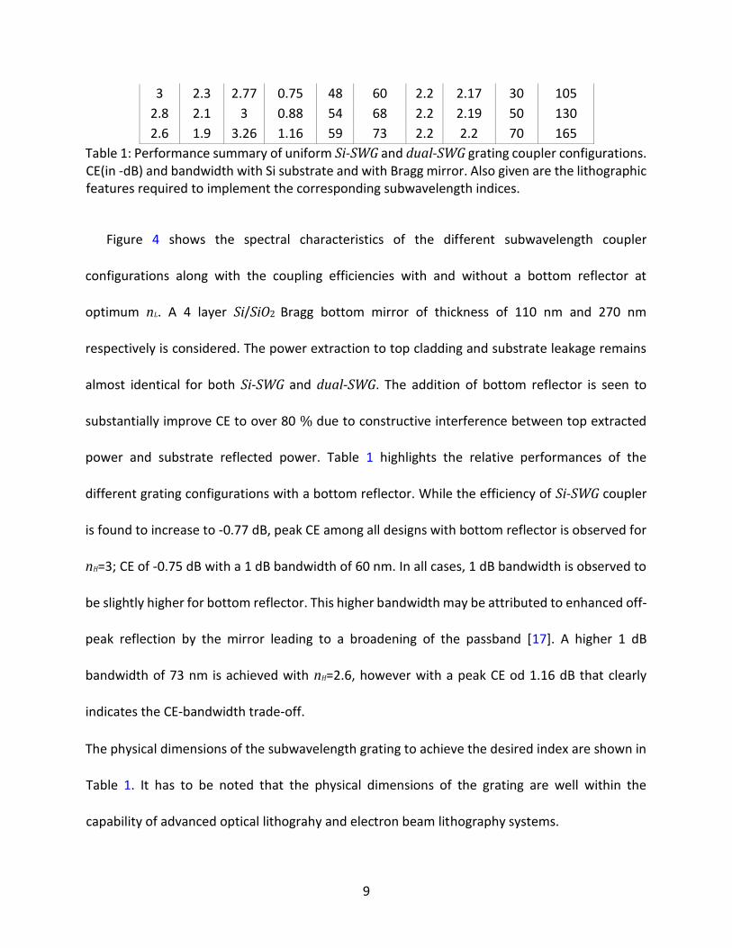
Table 1: Performance summary of uniform Si-SWG and dual-SWG grating coupler configurations. CE(in -dB) and bandwidth with Si substrate and with Bragg mirror. Also given are the lithographic features required to implement the corresponding subwavelength indices.
Figure 4 shows the spectral characteristics of the different subwavelength coupler
configurations along with the coupling efficiencies with and without a bottom reflector at
optimum nL. A 4 layer Si/SiO2 Bragg bottom mirror of thickness of 110 nm and 270 nm
respectively is considered. The power extraction to top cladding and substrate leakage remains
almost identical for both Si-SWG and dual-SWG. The addition of bottom reflector is seen to
substantially improve CE to over 80 % due to constructive interference between top extracted
power and substrate reflected power. Table 1 highlights the relative performances of the
different grating configurations with a bottom reflector. While the efficiency of Si-SWG coupler
is found to increase to -0.77 dB, peak CE among all designs with bottom reflector is observed for
nH=3; CE of -0.75 dB with a 1 dB bandwidth of 60 nm. In all cases, 1 dB bandwidth is observed to
be slightly higher for bottom reflector. This higher bandwidth may be attributed to enhanced off-
peak reflection by the mirror leading to a broadening of the passband [17]. A higher 1 dB
bandwidth of 73 nm is achieved with nH=2.6, however with a peak CE od 1.16 dB that clearly
indicates the CE-bandwidth trade-off.
The physical dimensions of the subwavelength grating to achieve the desired index are shown in
Table 1. It has to be noted that the physical dimensions of the grating are well within the
capability of advanced optical lithograhy and electron beam lithography systems.

10
3.1 Non-Uniform SWGCs
Fig 5: Schematic of non-uniform 2D subwavelength grating coupler design used in FDTD simulations.
As mentioned previously, one of the two primary loss mechanisms is the grating and fiber
mode mismatch. For a uniform grating, the power emission profile is an exponentially decaying
function (Pout = Pine−2αx) due to the leakage parameter α being constant in propagation direction.
However, a fiber mode has a Gaussian profile, which results in an overlap mismatch with the
grating field. The overlap is increased by designing the grating to scatter a Gaussian profile, which
requires progressive change in the scattering strength of the grating. For the subwavelength
structures, this can be achieved by tuning the period, which in turn modifies the subwavelength
index and hence the effective grating index.
A schematic of variable grating used for 2D FDTD is shown in fig.5. The scattered field for a
non-uniform grating with linear apodizations is determined by the non-uniform coupling
coefficient [18] as,
(9)

11
where G(x) is the normalized Gaussian profile determined by the fiber mode source and x the
propagation direction. The apodization implemented in the case of a Si-SWG was a linear chirp
function with nL varied from 1.9 to 3.2 and nH fixed at 3.46. With a fixed 50% duty cycle, period
was also continuously varied. The apodized grating was constructed by modifying eqn.4 as,
Here nLeff and nHeff are the effective indices (TE) of the low and high index subwavelength
regions respectively. From the above expression, the longitudinal grating period of the ith element
Λi can be extracted from eqn.6. For the dual-SWG, a two step apodization was employed whereby
the chirp function is linear upto nH after which both nL and nH are gradually increased till nH reaches
a maximum of 3.2 and nL=3.15. Such a dual stage apodization reduces the back reflection from
the subwavelength index region. The grating thus was constructed as,
The grating spectrum for these non-uniform couplers is plotted in fig.6. A top cladding
extraction of 70 % and substrate leakage of 30 % are similar to that observed in the case of
uniform couplers. However, the observed peak CE is observed to be 67 % and 61 % for Si-SWG
and dual-SWG respectively, which is about 10 % higher than the corresponding uniform
designs. With a Bragg mirror, the CE for Si-SWG is enhanced to 98.25 (-0.077 dB) % and 96.8 (-
0.14 dB) % for a dual-SWG with nH=3.

12
(a) (b)
Fig 6: Grating spectrum consisting of power extraction to top cladding, substrate leakage as well
as coupling efficiency with and without a Bragg mirror for (a) apodized Si-SWG and (b) apodized
dual-SWG with nH =3.
Fig.7 shows the normalized E-field intensities for both uniform and apodized couplers. The
higher coupling in case of apodized couplers can be attributed to the complete enclosure of the
in-
(a) (b)
Fig 7: Normalized E field intensities along with the fiber mode field for (a) uniform gratings, (b) apodized gratings.
cident fiber mode by the grating field which leads to a better mode overlap with the fiber field
compared to that of uniform couplers. Table 2 provides a performance summary of different

13
apodized subwavelength grating designs. In all designs, the peak CE is observed to be 10-14 %
higher than the corresponding optimized uniform coupler designs. For the design with the lowest
CE (i.e nH = 2.6), the observed 3 dB bandwidth was 95 nm, which is higher than previously
reported non-uniform subwavelength coupler designs. One of the crucial parameters in designing
SWG is the minimum dimension of the structures. For a desired refractive index, the choice of
SWG period has a direct implication on the minimum trench width of the grating. As discussed
earlier, large bandwidth requires lower dispersion (Eq. 5) that can achieve by using a lower SWG
period. For an SWG period of 300 nm, a minimum trench width of 13.5 nm would be required for
the apodized coupler, which could be achieved using e-beam lithography or 193 immersion
lithography. The minimum trench width could be increased to 26 nm with 400 nm period.
Availability of patterning technology and resolution could limit the SWG period choice.
CE(-dB) 1dB(nm) BOX(µm)
Si Bottom Si Bottom Si Bottom
Sub mirror Sub mirror Sub mirror
3.46 3.2 1.9 1.73 0.077 40 44 2.2 2.15
3.2 3.0 1.7 2.13 0.14 44 50 2.2 2.16
3.2 2.8 1.65 2.48 0.241 47 53 2.2 2.17
3.2 2.6 1.6 2.66 0.376 51 57 2.2 2.18
Ref[19] - - 1.97 0.42 - 66∗ - -
Ref[20] - - - 0.43 - 76∗ - -
Table 2: Performance summary of apodized Si-SWG and dual-SWG grating coupler
configurations. Max CE (in -dB) and bandwidth with Si substrate and the optimized BOX thickness
for a 4 layer bottom Bragg mirror. Comparison with references for simulated data only.∗ 3dB
bandwidth.

14
4 Conclusion
We have done a detailed studied of a subwavelength grating based couplers with the main
objective to explore ways to improve coupling efficiency and operation bandwidth. We observe
a trade-off between maximum achievable coupling efficiency and bandwidth. Based on the study,
we found that for uniform grating designs, the maximum CE can vary from -2.45 dB to -3.26 dB
per coupler with the operating 1 dB bandwidth being 43 nm and 59 nm respectfully. For non-
uniform designs the maximum CE can very from -1.73 dB to -2.66 dB with the corresponding 1
dB bandwidth varying from 40 to 51 nm. For uniform designs with a bottom reflector best CE is
observed for a dual-SWG design at -0.75 dB with a 1 dB bandwidth of 60 nm. For a non-uniform
couplers, best CE is observed for Si-SWG at -0.077 dB with the 1 dB bandwidth being 44 nm.
References
[1] B. B. Bakir, A. V. de Gyves, R. Orobtchouk, et al., “Low-Loss (¡1 dB) and
PolarizationInsensitive Edge Fiber Couplers Fabricated on 200-mm Silicon-on-Insulator
Wafers,” IEEE
Photonics Technol. Lett. 22, 739–741 (2010).
[2] M. Pu, L. Liu, H. Ou, et al., “Ultra-low-loss inverted taper coupler for silicon-on-insulator
ridge waveguide,” Opt. Commun. 283(19), 3678–3682 (2010).
[3] V. R. Almeida, R. R. Panepucci, and M. Lipson, “Nanotaper for compact mode conversion,”
Opt. Lett. 28, 1302–1304 (2003).

15
[4] D. Taillaert, P. Bienstman, and R. Baets, “Compact efficient broadband grating coupler for
silicon-on-insulator waveguides,” Opt. Lett. 29, 2749–2751 (2004).
[5] A. Mekis, S. Gloeckner, G. Masini, et al., “A Grating-Coupler-Enabled CMOS Photonics
Platform,” IEEE J. Sel. Top. Quantum Electron. 17, 597–608 (2011).
[6] G. Roelkens, D. V. Thourhout, and R. Baets, “High efficiency Silicon-on-Insulator grating
coupler based on a poly-Silicon overlay,” Opt. Express 14, 11622–11630 (2006).
[7] X. Xu, H. Subbaraman, J. Covey, et al., “Colorless grating couplers realized by interleaving
dispersion engineered subwavelength structures,” Opt. Lett. 38, 3588–3591 (2013).
[8] X. Chen and H. K. Tsang, “Polarization-independent grating couplers for silicon-on-insulator
nanophotonic waveguides,” Opt. Lett. 36, 796–798 (2011).
[9] R. Halir, A. Ortega-Monux, J. H. Schmid,˜ et al., “Recent Advances in Silicon Waveguide
Devices Using Sub-Wavelength Gratings,” IEEE J. Sel. Top. Quantum Electron. 20, 279–291
(2014).
[10] Q. Zhong, V. Veerasubramanian, Y. Wang, et al., “Focusing-curved subwavelength grating
couplers for ultra-broadband silicon photonics optical interfaces,” Opt. Express 22, 18224–
18231 (2014).
[11] D. H. Raguin and G. M. Morris, “Antireflection structured surfaces for the infrared spectral
region,” Appl. Opt. 32, 1154–1167 (1993).

16
[12] X. Chen, K. Xu, Z. Cheng, et al., “Wideband subwavelength gratings for coupling between
silicon-on-insulator waveguides and optical fibers,” Opt. Lett. 37, 3483–3485 (2012).
[13] W. S. Zaoui, M. F. Rosa, W. Vogel, et al., “Cost-effective CMOS-compatible grating couplers
with backside metal mirror and 69% coupling efficiency,” Opt. Express 20, B238—-B243
(2012).
[14] M. Antelius, K. B. Gylfason, and H. Sohlstrom, “An apodized SOI waveguide-to-fiber surface¨
grating coupler for single lithography silicon photonics,” Opt. Express 19, 3592–3598 (2011).
[15] S. K. Selvaraja, D. Vermeulen, M. Schaekers, et al., “Highly efficient grating coupler between
optical fiber and silicon photonic circuit,” in 2009 Conf. Lasers Electro-Optics 2009 Conf.
Quantum Electron. Laser Sci. Conf., 1–2 (2009).
[16] H. Zhang, C. Li, X. Tu, et al., “Efficient silicon nitride grating coupler with distributed Bragg
reflectors,” Opt. Express 22, 21800–21805 (2014).
[17] C. R. Doerr, L. Chen, Y. K. Chen, et al., “Wide Bandwidth Silicon Nitride Grating Coupler,”
IEEE Photonics Technol. Lett. 22, 1461–1463 (2010).
[18] R. Waldhausl, B. Schnabel, P. Dannberg,¨ et al., “Efficient Coupling into Polymer Waveguides
by Gratings,” Appl. Opt. 36, 9383–9390 (1997).
[19] D. Benedikovic, P. Cheben, J. H. Schmid, et al., “High-efficiency single etch step apodized
surface grating coupler using subwavelength structure,” Laser Photon. Rev. 8(6), L93—-L97
(2014).

17
[20] Y. Ding, C. Peucheret, H. Ou, et al., “Fully etched apodized grating coupler on the SOI
platform with -0.58 dB coupling efficiency,” Opt. Lett. 39, 5348–5350 (2014).