
High-Efficiency 20-A Synchronous Buck Converter … 21 I and set the OCL trip voltage as follows....
38
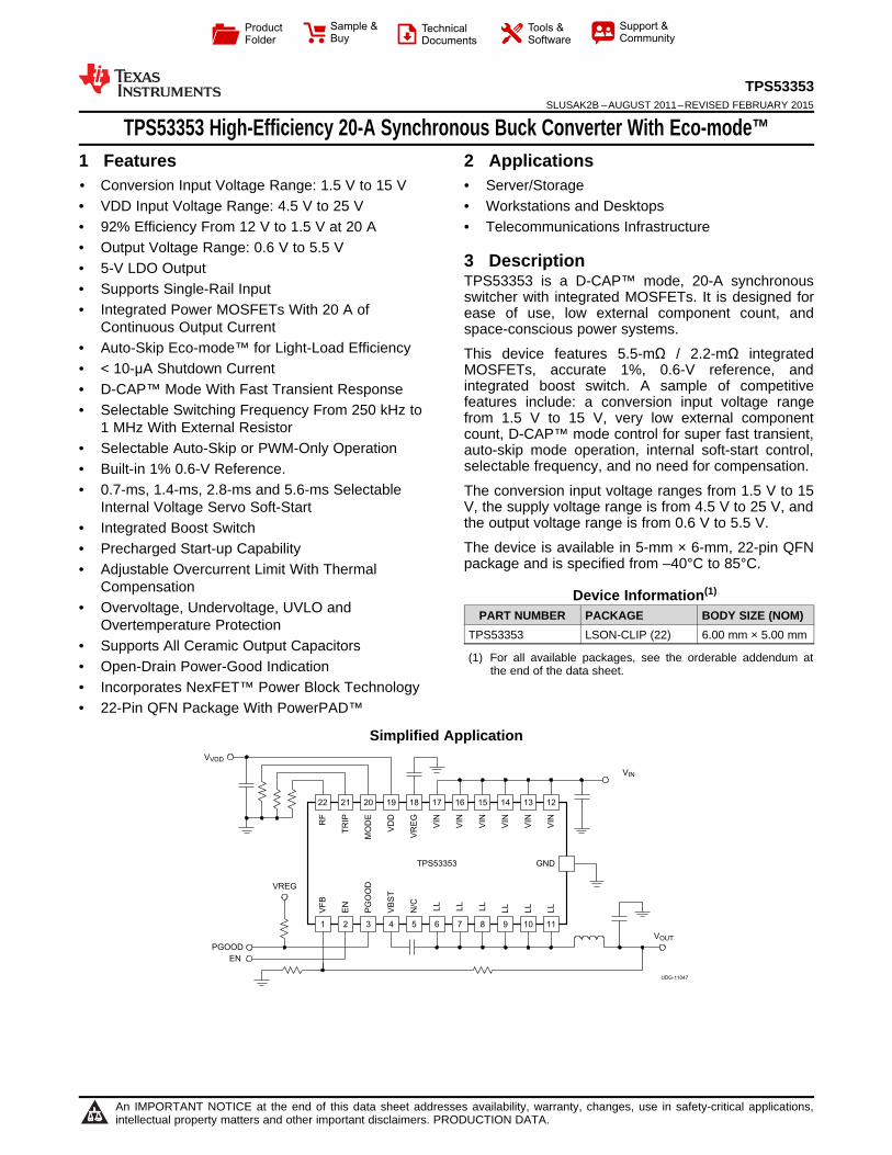
UDG-11047 RF TRIP MODE VDD VREG VIN VIN VIN VIN VIN VIN TPS53353 VFB EN PGOOD VBST N/C LL LL LL 1 2 3 4 5 6 7 8 9 10 11 22 21 20 19 18 17 16 15 14 13 12 VOUT VREG GND LL LL LL EN PGOOD VVDD VIN Product Folder Sample & Buy Technical Documents Tools & Software Support & Community TPS53353 SLUSAK2B – AUGUST 2011 – REVISED FEBRUARY 2015 TPS53353 High-Efficiency 20-A Synchronous Buck Converter With Eco-mode™ 1 Features 2 Applications 1• Conversion Input Voltage Range: 1.5 V to 15 V • Server/Storage • VDD Input Voltage Range: 4.5 V to 25 V • Workstations and Desktops • 92% Efficiency From 12 V to 1.5 V at 20 A • Telecommunications Infrastructure • Output Voltage Range: 0.6 V to 5.5 V 3 Description • 5-V LDO Output TPS53353 is a D-CAP™ mode, 20-A synchronous • Supports Single-Rail Input switcher with integrated MOSFETs. It is designed for • Integrated Power MOSFETs With 20 A of ease of use, low external component count, and Continuous Output Current space-conscious power systems. • Auto-Skip Eco-mode™ for Light-Load Efficiency This device features 5.5-mΩ / 2.2-mΩ integrated • < 10-μA Shutdown Current MOSFETs, accurate 1%, 0.6-V reference, and integrated boost switch. A sample of competitive • D-CAP™ Mode With Fast Transient Response features include: a conversion input voltage range • Selectable Switching Frequency From 250 kHz to from 1.5 V to 15 V, very low external component 1 MHz With External Resistor count, D-CAP™ mode control for super fast transient, • Selectable Auto-Skip or PWM-Only Operation auto-skip mode operation, internal soft-start control, selectable frequency, and no need for compensation. • Built-in 1% 0.6-V Reference. • 0.7-ms, 1.4-ms, 2.8-ms and 5.6-ms Selectable The conversion input voltage ranges from 1.5 V to 15 V, the supply voltage range is from 4.5 V to 25 V, and Internal Voltage Servo Soft-Start the output voltage range is from 0.6 V to 5.5 V. • Integrated Boost Switch The device is available in 5-mm × 6-mm, 22-pin QFN • Precharged Start-up Capability package and is specified from –40°C to 85°C. • Adjustable Overcurrent Limit With Thermal Compensation Device Information (1) • Overvoltage, Undervoltage, UVLO and PART NUMBER PACKAGE BODY SIZE (NOM) Overtemperature Protection TPS53353 LSON-CLIP (22) 6.00 mm × 5.00 mm • Supports All Ceramic Output Capacitors (1) For all available packages, see the orderable addendum at • Open-Drain Power-Good Indication the end of the data sheet. • Incorporates NexFET™ Power Block Technology • 22-Pin QFN Package With PowerPAD™ Simplified Application 1 An IMPORTANT NOTICE at the end of this data sheet addresses availability, warranty, changes, use in safety-critical applications, intellectual property matters and other important disclaimers. PRODUCTION DATA.
Transcript of High-Efficiency 20-A Synchronous Buck Converter … 21 I and set the OCL trip voltage as follows....
UDG-11047
RF
TR
IP
MO
DE
VD
D
VR
EG
VIN
VIN
VIN
VIN
VIN
VIN
TPS53353
VF
B
EN
PG
OO
D
VB
ST
N/C
LL
LL
LL
1 2 3 4 5 6 7 8 9 10 11
22 21 20 19 18 17 16 15 14 13 12
VOUT
VREG
GND
LL
LL
LL
EN
PGOOD
VVDD
VIN
Product
Folder
Sample &Buy
Technical
Documents
Tools &
Software
Support &Community
TPS53353SLUSAK2B –AUGUST 2011–REVISED FEBRUARY 2015
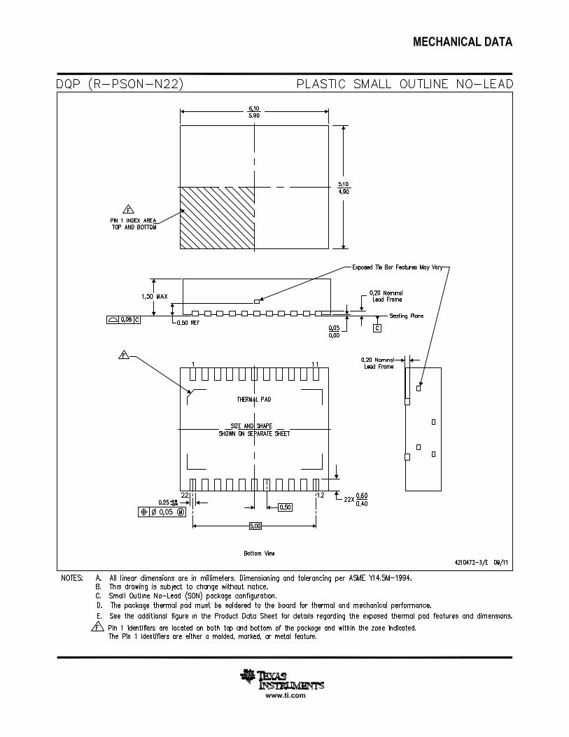
TPS53353 High-Efficiency 20-A Synchronous Buck Converter With Eco-mode™1 Features 2 Applications1• Conversion Input Voltage Range: 1.5 V to 15 V • Server/Storage• VDD Input Voltage Range: 4.5 V to 25 V • Workstations and Desktops• 92% Efficiency From 12 V to 1.5 V at 20 A • Telecommunications Infrastructure• Output Voltage Range: 0.6 V to 5.5 V
3 Description• 5-V LDO OutputTPS53353 is a D-CAP™ mode, 20-A synchronous• Supports Single-Rail Input switcher with integrated MOSFETs. It is designed for
• Integrated Power MOSFETs With 20 A of ease of use, low external component count, andContinuous Output Current space-conscious power systems.
• Auto-Skip Eco-mode™ for Light-Load Efficiency This device features 5.5-mΩ / 2.2-mΩ integrated• < 10-μA Shutdown Current MOSFETs, accurate 1%, 0.6-V reference, and
integrated boost switch. A sample of competitive• D-CAP™ Mode With Fast Transient Responsefeatures include: a conversion input voltage range• Selectable Switching Frequency From 250 kHz to from 1.5 V to 15 V, very low external component1 MHz With External Resistor count, D-CAP™ mode control for super fast transient,
• Selectable Auto-Skip or PWM-Only Operation auto-skip mode operation, internal soft-start control,selectable frequency, and no need for compensation.• Built-in 1% 0.6-V Reference.
• 0.7-ms, 1.4-ms, 2.8-ms and 5.6-ms Selectable The conversion input voltage ranges from 1.5 V to 15V, the supply voltage range is from 4.5 V to 25 V, andInternal Voltage Servo Soft-Startthe output voltage range is from 0.6 V to 5.5 V.• Integrated Boost SwitchThe device is available in 5-mm × 6-mm, 22-pin QFN• Precharged Start-up Capabilitypackage and is specified from –40°C to 85°C.• Adjustable Overcurrent Limit With Thermal
Compensation Device Information(1)
• Overvoltage, Undervoltage, UVLO and PART NUMBER PACKAGE BODY SIZE (NOM)Overtemperature Protection
TPS53353 LSON-CLIP (22) 6.00 mm × 5.00 mm• Supports All Ceramic Output Capacitors
(1) For all available packages, see the orderable addendum at• Open-Drain Power-Good Indication the end of the data sheet.• Incorporates NexFET™ Power Block Technology• 22-Pin QFN Package With PowerPAD™
Simplified Application
1
An IMPORTANT NOTICE at the end of this data sheet addresses availability, warranty, changes, use in safety-critical applications,intellectual property matters and other important disclaimers. PRODUCTION DATA.
TPS53353SLUSAK2B –AUGUST 2011–REVISED FEBRUARY 2015 www.ti.com
Table of Contents7.3 Feature Description................................................. 141 Features .................................................................. 17.4 Device Functional Modes........................................ 172 Applications ........................................................... 1
8 Application and Implementation ........................ 203 Description ............................................................. 18.1 Application Information............................................ 204 Revision History..................................................... 28.2 Typical Applications ................................................ 205 Pin Configuration and Functions ......................... 3
9 Power Supply Recommendations ...................... 276 Specifications......................................................... 410 Layout................................................................... 276.1 Absolute Maximum Ratings ...................................... 4
10.1 Layout Guidelines ................................................. 276.2 ESD Ratings.............................................................. 410.2 Layout Example .................................................... 286.3 Recommended Operating Conditions....................... 4
11 Device and Documentation Support ................. 296.4 Thermal Information .................................................. 511.1 Trademarks ........................................................... 296.5 Electrical Characteristics........................................... 511.2 Electrostatic Discharge Caution............................ 296.6 Typical Characteristics .............................................. 711.3 Glossary ................................................................ 297 Detailed Description ............................................ 13
12 Mechanical, Packaging, and Orderable7.1 Overview ................................................................. 13Information ........................................................... 297.2 Functional Block Diagram ....................................... 13
4 Revision HistoryNOTE: Page numbers for previous revisions may differ from page numbers in the current version.
Changes from Revision A (April 2012) to Revision B Page
• Added Pin Configuration and Functions section, ESD Ratings table, Feature Description section, Device FunctionalModes, Application and Implementation section, Power Supply Recommendations section, Layout section, Deviceand Documentation Support section, and Mechanical, Packaging, and Orderable Information section .............................. 1
Changes from Original (AUGUST 2011) to Revision A Page
• Changed conversion input voltage from "3 V" to "1.5 V"........................................................................................................ 1• Changed VIN input voltage range minimum from "3 V" to "1.5 V" ......................................................................................... 3• Changed to correct typographical error in THERMAL INFORMATION table......................................................................... 4• Changed VIN (main supply) input voltage range minimum from "3 V' to "1.5 V" in Recommended Operating Conditions... 4• Changed conversion input voltage range from "3 V" to "1.5" in Overview........................................................................... 13• Added note to the Feature Description................................................................................................................................. 14• Changed "ripple injection capacitor" to "ripple injection resistor" in the last bullet of the section ........................................ 27
2 Submit Documentation Feedback Copyright © 2011–2015, Texas Instruments Incorporated
Product Folder Links: TPS53353
VFB
EN
PGOOD
1
2
3
4
5
6
7
8
9
10
11 12
13
14
15
16
17GND
PowerPadTM
18
19
20
21
22
VBST
TRIP
MODE
N/C
LL
LL
LL
LL
LL
LL
RF
VDD
VREG
VIN
VIN
VIN
VIN
VIN
VIN
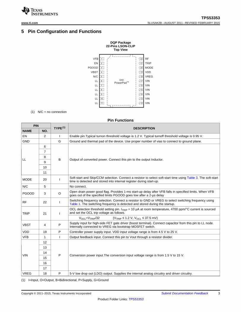
TPS53353www.ti.com SLUSAK2B –AUGUST 2011–REVISED FEBRUARY 2015
5 Pin Configuration and Functions
DQP Package22-Pins LSON-CLIP
Top View
(1) N/C = no connection
Pin FunctionsPIN
TYPE (1) DESCRIPTIONNAME NO.EN 2 I Enable pin.Typical turnon threshold voltage is 1.2 V. Typical turnoff threshold voltage is 0.95 V.GND G Ground and thermal pad of the device. Use proper number of vias to connect to ground plane.
678
LL B Output of converted power. Connect this pin to the output Inductor.91011
Soft-start and Skip/CCM selection. Connect a resistor to select soft-start time using Table 3. The soft-startMODE 20 I time is detected and stored into internal register during start-up.N/C 5 No connect.
Open drain power good flag. Provides 1-ms start-up delay after VFB falls in specified limits. When VFBPGOOD 3 O goes out of the specified limits PGOOD goes low after a 2-µs delaySwitching frequency selection. Connect a resistor to GND or VREG to select switching frequency usingRF 22 I Table 1. The switching frequency is detected and stored during the startup.OCL detection threshold setting pin. ITRIP = 10 µA at room temperature, 4700 ppm/°C current is sourcedand set the OCL trip voltage as follows.TRIP 21 Ispace VOCL=VTRIP/32 (VTRIP ≤ 1.2 V, VOCL ≤ 37.5 mV)Supply input for high-side FET gate driver (boost terminal). Connect capacitor from this pin to LL node.VBST 4 P Internally connected to VREG via bootstrap MOSFET switch.
VDD 19 P Controller power supply input. VDD input voltage range is from 4.5 V to 25 V.VFB 1 I Output feedback input. Connect this pin to Vout through a resistor divider.
121314
VIN P Conversion power input.The conversion input voltage range is from 1.5 V to 15 V.151617
VREG 18 P 5-V low drop out (LDO) output. Supplies the internal analog circuitry and driver circuitry.
(1) I=Input, O=Output, B=Bidirectional, P=Supply, G=Ground
Copyright © 2011–2015, Texas Instruments Incorporated Submit Documentation Feedback 3
Product Folder Links: TPS53353

TPS53353SLUSAK2B –AUGUST 2011–REVISED FEBRUARY 2015 www.ti.com
6 Specifications
6.1 Absolute Maximum Ratings (1)
MIN MAX UNITVIN (main supply) –0.3 25VDD –0.3 28
Input voltage range VBST –0.3 32 VVBST(with respect to LL) –0.3 7EN, TRIP, VFB, RF, MODE –0.3 7
DC –2 25LL
Pulse < 20ns, E=5 μJ –7 27Output voltage range V
PGOOD, VREG –0.3 7GND –0.3 0.3
Source/Sink current VBST 50 mAOperating free-air temperature, TA –40 85Junction temperature, TJ –40 150 °CLead temperature 1,6 mm (1/16 inch) from case for 10 seconds 300Storage temperature, Tstg –55 150 °C
(1) Stresses beyond those listed under Absolute Maximum Ratings may cause permanent damage to the device. These are stress ratingsonly and functional operation of the device at these or any other conditions beyond those indicated under Recommended OperatingConditions is not implied. Exposure to absolute-maximum-rated conditions for extended periods may affect device reliability.
6.2 ESD RatingsVALUE UNIT
Human-body model (HBM), per ANSI/ESDA/JEDEC JS-001 (1) 2000V(ESD) Electrostatic discharge VCharged-device model (CDM), per JEDEC specification JESD22- 500
C101 (2)
(1) JEDEC document JEP155 states that 500-V HBM allows safe manufacturing with a standard ESD control process.(2) JEDEC document JEP157 states that 250-V CDM allows safe manufacturing with a standard ESD control process.
6.3 Recommended Operating Conditionsover operating free-air temperature range (unless otherwise noted)
MIN MAX UNITVIN (main supply) 1.5 15VDD 4.5 25
Input voltage range VBST 4.5 28 VVBST(with respect to LL) 4.5 6.5EN, TRIP, VFB, RF, MODE –0.1 6.5
Output voltage range LL –1 22V
PGOOD, VREG –0.1 6.5Junction temperature range, TJ –40 125 °C
4 Submit Documentation Feedback Copyright © 2011–2015, Texas Instruments Incorporated
Product Folder Links: TPS53353

TPS53353www.ti.com SLUSAK2B –AUGUST 2011–REVISED FEBRUARY 2015
6.4 Thermal InformationTPS53353
THERMAL METRIC (1) DQP (LSON-CLIP) UNIT22 PINS
θJA Junction-to-ambient thermal resistance 27.2θJCtop Junction-to-case (top) thermal resistance 17.1θJB Junction-to-board thermal resistance 5.9
°C/WψJT Junction-to-top characterization parameter 0.8ψJB Junction-to-board characterization parameter 5.8θJCbot Junction-to-case (bottom) thermal resistance 1.2
(1) For more information about traditional and new thermal metrics, see the IC Package Thermal Metrics application report, SPRA953.
6.5 Electrical CharacteristicsOver recommended free-air temperature range, VVDD= 12 V (unless otherwise noted)
PARAMETER CONDITIONS MIN TYP MAX UNITSUPPLY CURRENT
VIN pin power conversion inputVVIN 1.5 15 VvoltageVVDD Supply input voltage 4.5 25 VIVIN(leak) VIN pin leakage current VEN = 0 V 1 µAIVDD VDD supply current TA = 25°C, No load, VEN = 5 V, VVFB = 0.630 V 420 590 µAIVDDSDN VDD shutdown current TA = 25°C, No load, VEN = 0 V 10 µAINTERNAL REFERENCE VOLTAGEVVFB VFB regulation voltage CCM condition (1) 0.6 V
TA = 25°C 0.597 0.6 0.603VVFB VFB regulation voltage 0°C ≤ TA ≤ 85°C 0.5952 0.6 0.6048 V
–40°C ≤ TA ≤ 85°C 0.594 0.6 0.606IVFB VFB input current VVFB = 0.630 V, TA = 25°C 0.01 0.2 µALDO OUTPUTVVREG LDO output voltage 0 mA ≤ IVREG ≤ 30 mA 4.77 5 5.36 VIVREG LDO output current (1) Maximum current allowed from LDO 30 mAVDO Low drop out voltage VVDD = 4.5 V, IVREG = 30 mA 230 mVBOOT STRAP SWITCHVFBST Forward voltage VVREG-VBST, IF = 10 mA, TA = 25°C 0.1 0.2 VIVBSTLK VBST leakage current VVBST = 23 V, VSW = 17 V, TA = 25°C 0.01 1.5 µADUTY AND FREQUENCY CONTROLtOFF(min) Minimum off time TA = 25°C 150 260 400 ns
VIN = 17 V, VOUT = 0.6 V, RRF = 39 kΩ,tON(min) Minimum on time 35 nsTA = 25 °C (1)
SOFT STARTRMODE = 39 kΩ 0.7RMODE = 100 kΩ 1.4Internal soft-start time fromtSS msVOUT = 0 V to 95% of VOUT RMODE = 200 kΩ 2.8RMODE = 470 kΩ 5.6
INTERNAL MOSFETsRDS(on)H High-side MOSFET on-resistance TA = 25 °C 5.5
mΩRDS(on)L Low-side MOSFET on-resistance TA = 25 °C 2.2
(1) Ensured by design. Not production tested.
Copyright © 2011–2015, Texas Instruments Incorporated Submit Documentation Feedback 5
Product Folder Links: TPS53353

TPS53353SLUSAK2B –AUGUST 2011–REVISED FEBRUARY 2015 www.ti.com
Electrical Characteristics (continued)Over recommended free-air temperature range, VVDD= 12 V (unless otherwise noted)
PARAMETER CONDITIONS MIN TYP MAX UNITPOWERGOOD
PG in from lower 92.5% 95% 98.5%VTHPG PG threshold PG in from higher 107.5% 110% 112.5%
PG hysteresis 2.5% 5% 7.5%RPG PG transistor on-resistance 15 30 55 ΩtPGDEL PG delay Delay for PG in 0.8 1 1.2 msLOGIC THRESHOLD AND SETTING CONDITIONS
Enable 1.8VEN EN Voltage V
Disable 0.6IEN EN Input current VEN = 5 V 1 µA
RRF = 0 Ω to GND, TA = 25°C (2) 200 250 300RRF = 187 kΩ to GND, TA = 25°C (2) 250 300 350RRF = 619 kΩ, to GND, TA = 25°C (2) 350 400 450RRF = Open, TA= 25°C (2) 450 500 550
fSW Switching frequency kHzRRF = 866 kΩ to VREG, TA = 25°C (2) 580 650 720RRF = 309 kΩ to VREG, TA = 25°C (2) 670 750 820RRF = 124 kΩ to VREG, TA = 25°C (2) 770 850 930RRF = 0 Ω to VREG, TA = 25°C (2) 880 970 1070
PROTECTION: CURRENT SENSEITRIP TRIP source current VTRIP = 1 V, TA = 25°C 9.4 10 10.6 µA
TRIP current temperatureTCITRIP On the basis of 25°C (1) 4700 ppm/°CcoeffficientCurrent limit threshold settingVTRIP VTRIP-GND 0.4 1.2 Vrange
VTRIP = 1.2 V 32 37.5 43VOCL Current limit threshold mV
VTRIP = 0.4 7.5 12.5 17.5VTRIP = 1.2 V –160 –150 –140
VOCLN Negative current limit threshold mVVTRIP = 0.4 V –58 –50 –42Positive 3 15
VAZCADJ Auto zero cross adjustable range mVNegative –15 –3
PROTECTION: UVP and OVPVOVP OVP trip threshold OVP detect 115% 120% 125%tOVPDEL OVP proprogation delay VFB delay with 50-mV overdrive 1 µsVUVP Output UVP trip threshold UVP detect 65% 70% 75%tUVPDEL Output UVP proprogation delay 0.8 1 1.2 mstUVPEN Output UVP enable delay From enable to UVP workable 1.8 2.6 3.2 msUVLO
Wake up 4 4.2 4.33VUVVREG VREG UVLO threshold V
Hysteresis 0.25THERMAL SHUTDOWN
Shutdown temperature (1) 145TSDN Thermal shutdown threshold °C
Hysteresis (1) 10
(2) Not production tested. Test condition is VIN= 12 V, VOUT= 1.1 V, IOUT = 10 A using application circuit shown in Figure 38.
6 Submit Documentation Feedback Copyright © 2011–2015, Texas Instruments Incorporated
Product Folder Links: TPS53353

1
10
100
1000
0.01 0.1 1 10 20Output Current (A)
Sw
itchi
ng F
requ
ency
(kH
z)
FCCMSkip Mode
VIN = 12 VVOUT = 1.1 VfSW = 300 kHz
G001
1
10
100
1000
0.01 0.1 1 10 20Output Current (A)
Sw
itchi
ng F
requ
ency
(kH
z)
FCCMSkip Mode
VIN = 12 VVOUT = 1.1 VfSW = 500 kHz
G001
0
2
4
6
8
10
12
14
16
−40 −25 −10 5 20 35 50 65 80 95 110 125Junction Temperature (°C)
TR
IP P
in C
urre
nt (
µA)
VVDD = 12 V 0
20
40
60
80
100
120
140
−40 −25 −10 5 20 35 50 65 80 95 110 125Junction Temperature (°C)
OV
P/U
VP
Trip
Thr
esho
ld (
%)
OVPUVP
0
100
200
300
400
500
600
700
−40 −25 −10 5 20 35 50 65 80 95 110 125Junction Temperature (°C)
VD
D S
uppl
y C
urre
nt (
µA)
VEN = 5V VVDD = 12 V VVFB = 0.63 V No Load
0
1
2
3
4
5
6
7
−40 −25 −10 5 20 35 50 65 80 95 110 125Junction Temperature (°C)
VD
D S
hutd
own
Cur
rent
(µA
)
VEN = 0 V VVDD = 12 V No Load
TPS53353www.ti.com SLUSAK2B –AUGUST 2011–REVISED FEBRUARY 2015
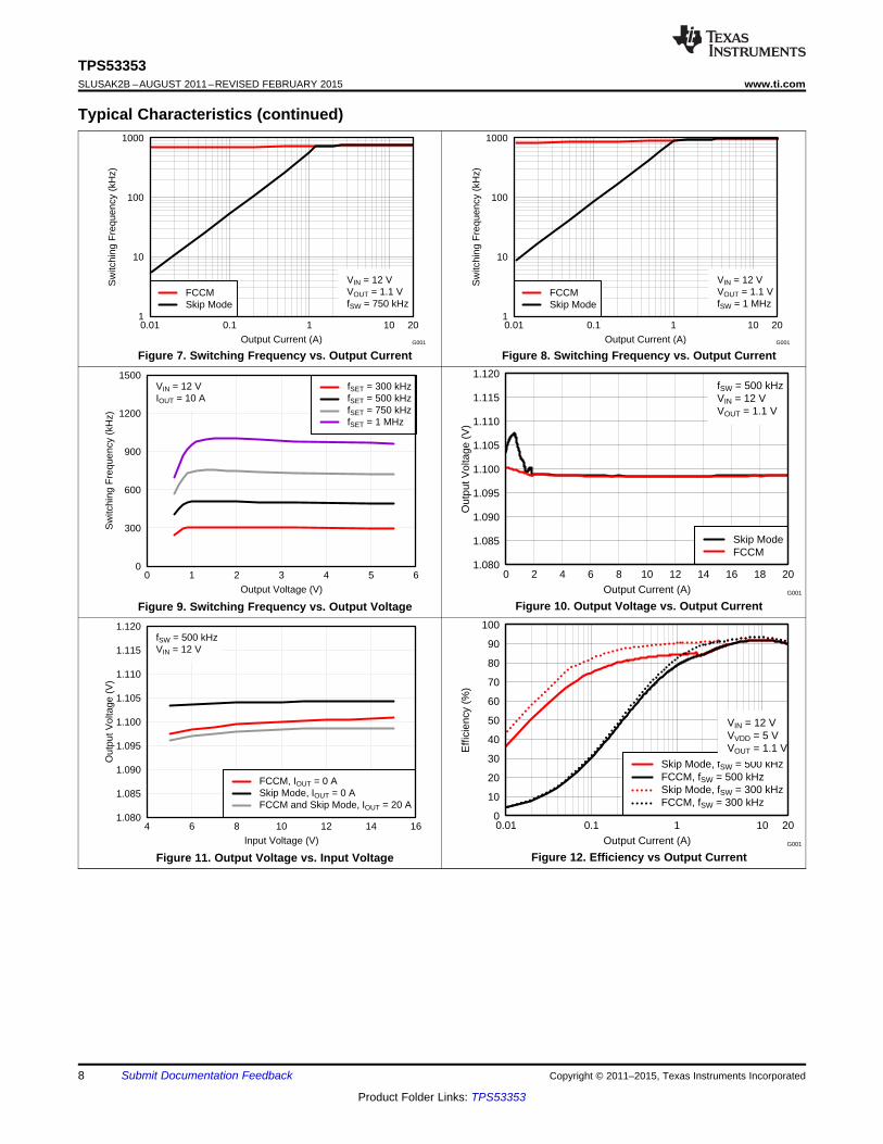
6.6 Typical Characteristics
Figure 1. VDD Supply Current vs. Junction Temperature Figure 2. VDD Shutdown Current vs. Junction Temperature
Figure 3. TRIP Pin Current vs. Junction Temperature Figure 4. OVP/UVP Trip Threshold vs. Junction Temperature
Figure 5. Switching Frequency vs. Output Current Figure 6. Switching Frequency vs. Output Current
Copyright © 2011–2015, Texas Instruments Incorporated Submit Documentation Feedback 7
Product Folder Links: TPS53353
1.080
1.085
1.090
1.095
1.100
1.105
1.110
1.115
1.120
4 6 8 10 12 14 16Input Voltage (V)
Out
put V
olta
ge (
V)
FCCM, IOUT = 0 ASkip Mode, IOUT = 0 AFCCM and Skip Mode, IOUT = 20 A
fSW = 500 kHzVIN = 12 V
0
10
20
30
40
50
60
70
80
90
100
0.01 0.1 1 10 20Output Current (A)
Effi
cien
cy (
%)
Skip Mode, fSW = 500 kHzFCCM, fSW = 500 kHzSkip Mode, fSW = 300 kHzFCCM, fSW = 300 kHz
VIN = 12 VVVDD = 5 VVOUT = 1.1 V
G001
0
300
600
900
1200
1500
0 1 2 3 4 5 6Output Voltage (V)
Sw
itchi
ng F
requ
ency
(kH
z)
fSET = 300 kHzfSET = 500 kHzfSET = 750 kHzfSET = 1 MHz
VIN = 12 VIOUT = 10 A
1.080
1.085
1.090
1.095
1.100
1.105
1.110
1.115
1.120
0 2 4 6 8 10 12 14 16 18 20Output Current (A)
Out
put V
olta
ge (
V)
Skip ModeFCCM
fSW = 500 kHzVIN = 12 VVOUT = 1.1 V
G001
1
10
100
1000
0.01 0.1 1 10 20Output Current (A)
Sw
itchi
ng F
requ
ency
(kH
z)
FCCMSkip Mode
VIN = 12 VVOUT = 1.1 VfSW = 750 kHz
G001
1
10
100
1000
0.01 0.1 1 10 20Output Current (A)
Sw
itchi
ng F
requ
ency
(kH
z)
FCCMSkip Mode
VIN = 12 VVOUT = 1.1 VfSW = 1 MHz
G001
TPS53353SLUSAK2B –AUGUST 2011–REVISED FEBRUARY 2015 www.ti.com
Typical Characteristics (continued)
Figure 7. Switching Frequency vs. Output Current Figure 8. Switching Frequency vs. Output Current
Figure 10. Output Voltage vs. Output CurrentFigure 9. Switching Frequency vs. Output Voltage
Figure 12. Efficiency vs Output CurrentFigure 11. Output Voltage vs. Input Voltage
8 Submit Documentation Feedback Copyright © 2011–2015, Texas Instruments Incorporated
Product Folder Links: TPS53353
Time (2 ms/div)
LL (5 V/div)
VOUT
(20 mV/div)
IL
(5 A/div)
FCCM
VIN
= 12 V
IOUT
= 0 A
Time (1 ms/div)
LL (5 V/div)
VOUT
(20 mV/div)
IL
(5 A/div)
Skip Mode
VIN
= 12 V
IOUT
= 0 A
VIN
(5 V/div)
VOUT
(0.5 V/div)
VREG(5 V/div)
PGOOD (5 V/div)
VEN
= 5 V
VDD
= VIN
IOUT
= 20 A
Time (2 ms/div)
VIN
= 12 V
IOUT
= 20 A EN (5 V/div)
VOUT
(0.5 V/div)
VREG(5 V/div)
PGOOD (5 V/div)
Time (20 ms/div)
VIN
= 12 V
IOUT
= 20 A EN (5 V/div)
VOUT
(0.5 V/div)
VREG(5 V/div)
PGOOD (5 V/div)
Time (1 ms/div)
VIN
= 12 V
IOUT
= 0 AEN (5 V/div)
VOUT
(0.5 V/div)
VREG(5 V/div)
PGOOD (5 V/div)
0.5 V pre-biased
Time (1 ms/div)
TPS53353www.ti.com SLUSAK2B –AUGUST 2011–REVISED FEBRUARY 2015
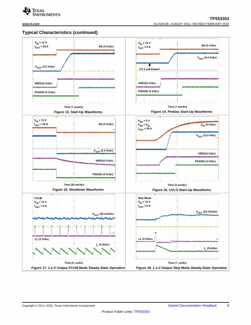
Typical Characteristics (continued)
Figure 14. Prebias Start-Up WaveformsFigure 13. Start-Up Waveforms
Figure 15. Shutdown Waveforms Figure 16. UVLO Start-Up Waveforms
Figure 17. 1.1-V Output FCCM Mode Steady-State Operation Figure 18. 1.1-V Output Skip Mode Steady-State Operation
Copyright © 2011–2015, Texas Instruments Incorporated Submit Documentation Feedback 9
Product Folder Links: TPS53353
Time (10 ms/div)
IOUT from 20 A to 25 A
VIN = 12 VVOUT (1 V/div)
LL (10 V/div)
IL (10 A/div)
PGOOD (5 V/div)
Time (10 ms/div)
IOUT 2 A then Short Output
VIN = 12 V
VOUT (1 V/div)
LL (10 V/div)
IL (10 A/div)
IOUT (25 A/div)
FCCM
VIN
= 12 V, VOUT
= 1.1 V
IOUT
from 0 A to 10 A, 2.5 A/ms
Time (100 ms/div)
VOUT
(20 mV/div)
IOUT
(5 A/div)
Skip Mode
VIN
= 12 V, VOUT
= 1.1 V
IOUT
from 0 A to 10 A, 2.5 A/ms
Time (100 ms/div)
VOUT
(20 mV/div)
IOUT
(5 A/div)
Time (200 ms/div)
LL (5 V/div)
VOUT
(20 mV/div)
IL
(5 A/div)
Skip Mode
VIN
= 12 V
VOUT
= 1.1 V
Skip Mode
VIN
= 12 V
VOUT
= 1.1 V
Time (200 ms/div)
LL (5 V/div)
VOUT
(20 mV/div)
IL
(5 A/div)
TPS53353SLUSAK2B –AUGUST 2011–REVISED FEBRUARY 2015 www.ti.com
Typical Characteristics (continued)
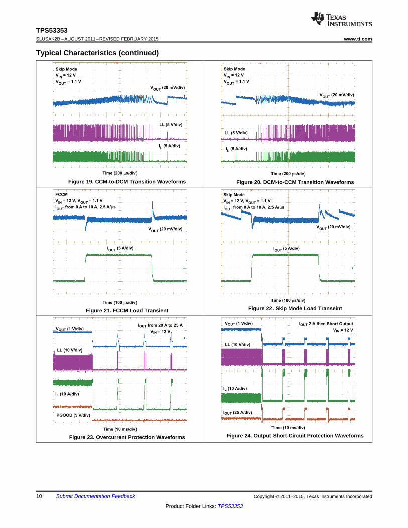
Figure 19. CCM-to-DCM Transition Waveforms Figure 20. DCM-to-CCM Transition Waveforms
Figure 22. Skip Mode Load TranseintFigure 21. FCCM Load Transient
Figure 24. Output Short-Circuit Protection WaveformsFigure 23. Overcurrent Protection Waveforms
10 Submit Documentation Feedback Copyright © 2011–2015, Texas Instruments Incorporated
Product Folder Links: TPS53353
70
75
80
85
90
95
100
0 2 4 6 8 10 12 14 16 18 20Output Current (A)
Effi
cien
cy (
%)
VOUT = 5.0 VVOUT = 3.3 VVOUT = 1.8 VVOUT = 1.5 VVOUT = 1.2 VVOUT = 1.1 VVOUT = 1.0 V
FCCMVIN = 12 VVVDD = 5 VfSW = 300 kHz
G001
70
75
80
85
90
95
100
0 2 4 6 8 10 12 14 16 18 20Output Current (A)
Effi
cien
cy (
%)
VOUT = 5.0 VVOUT = 3.3 VVOUT = 1.8 VVOUT = 1.5 VVOUT = 1.2 VVOUT = 1.1 VVOUT = 1.0 V
Skip ModeVIN = 12 VVVDD = 5 VfSW = 300 kHz
G000
20
30
40
50
60
70
80
90
0 2 4 6 8 10 12 14 16 18 20Output Current (A)
Am
bien
t Tem
pera
ture
(°C
)
400 LFM200 LFM100 LFMNatural Convection
VIN = 12 VVOUT = 5 VfSW = 500 kHz
G000
Time (1 s/div)
VIN
= 12 V
IOUT
= 20 A
EN (5 V/div)
VOUT
(1 V/div)
PGOOD (5 V/div)
20
30
40
50
60
70
80
90
0 2 4 6 8 10 12 14 16 18 20Output Current (A)
Am
bien
t Tem
pera
ture
(°C
)
All Levels of Air Flow
VIN = 12 VVOUT = 1.2 VfSW = 500 kHz
G000
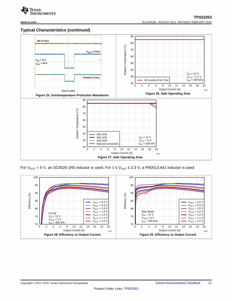
TPS53353www.ti.com SLUSAK2B –AUGUST 2011–REVISED FEBRUARY 2015
Typical Characteristics (continued)
Figure 26. Safe Operating AreaFigure 25. Overtemperature Protection Waveforms
Figure 27. Safe Operating Area
For VOUT = 5 V, an SC5026-1R0 inductor is used. For 1 ≤ VOUT ≤ 3.3 V, a PA0513.441 inductor is used
Figure 28. Efficiency vs Output Current Figure 29. Efficiency vs Output Current
Copyright © 2011–2015, Texas Instruments Incorporated Submit Documentation Feedback 11
Product Folder Links: TPS53353

70
75
80
85
90
95
100
0 2 4 6 8 10 12 14 16 18 20Output Current (A)
Effi
cien
cy (
%)
VOUT = 1.8 VVOUT = 1.5 VVOUT = 1.2 VVOUT = 1.1 VVOUT = 1.0 V
FCCMVIN = 5 VVVDD = 5 VfSW = 500 kHz
G001
70
75
80
85
90
95
100
0 2 4 6 8 10 12 14 16 18 20Output Current (A)
Effi
cien
cy (
%)
VOUT = 1.8 VVOUT = 1.5 VVOUT = 1.2 VVOUT = 1.1 VVOUT = 1.0 V
Skip ModeVIN = 5 VVVDD = 5 VfSW = 500 kHz
G001
70
75
80
85
90
95
100
0 2 4 6 8 10 12 14 16 18 20Output Current (A)
Effi
cien
cy (
%)
VOUT = 5.0 VVOUT = 3.3 VVOUT = 1.8 VVOUT = 1.5 VVOUT = 1.2 VVOUT = 1.1 VVOUT = 1.0 V
FCCMVIN = 12 VVVDD = 5 VfSW = 500 kHz
G000
70
75
80
85
90
95
100
0 2 4 6 8 10 12 14 16 18 20Output Current (A)
Effi
cien
cy (
%)
VOUT = 5.0 VVOUT = 3.3 VVOUT = 1.8 VVOUT = 1.5 VVOUT = 1.2 VVOUT = 1.1 VVOUT = 1.0 V
Skip ModeVIN = 12 VVVDD = 5 VfSW = 500 kHz
G000
TPS53353SLUSAK2B –AUGUST 2011–REVISED FEBRUARY 2015 www.ti.com
Typical Characteristics (continued)
Figure 30. Efficiency vs Output Current Figure 31. Efficiency vs Output Current
Figure 32. Efficiency vs Output Current Figure 33. Efficiency vs Output Current
12 Submit Documentation Feedback Copyright © 2011–2015, Texas Instruments Incorporated
Product Folder Links: TPS53353
Shutdown VREG
VDDOK
LL
TPS53353
tON
One-
Shot
Control
Logic
+
+ OCP
ZC
GND
LL
XCON
GND
+
1.2 V/0.95 V
EN
UVP/OVP
Logic
+THOK 145°C/
135°C
+
4.2 V/
3.95 V
VIN
VBST
Fault
LL
GND
RF
++
PWM
+ OV
+20%
UV+0.6 V –30%Delay
SS0.6 V
VFB
TRIP
Enable
+
+
Delay
0.6 V +10/15%
0.6 V –5/10%
PGOOD
Control Logic
· On/Off time
· Minimum On/Off
· Light load
· OVP/UVP
· FCCM/Skip
UDG-11048
10 ?A
VREG
+
SS
FCCM/
SkipDecode
MODE
VDD
Ramp
Compensation
+
LDO
EN
TPS53353www.ti.com SLUSAK2B –AUGUST 2011–REVISED FEBRUARY 2015
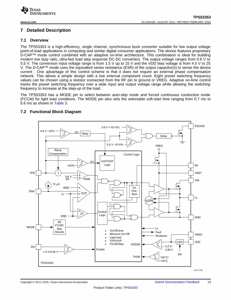
7 Detailed Description
7.1 OverviewThe TPS53353 is a high-efficiency, single channel, synchronous buck converter suitable for low output voltagepoint-of-load applications in computing and similar digital consumer applications. The device features proprietaryD-CAP™ mode control combined with an adaptive on-time architecture. This combination is ideal for buildingmodern low duty ratio, ultra-fast load step response DC-DC converters. The output voltage ranges from 0.6 V to5.5 V. The conversion input voltage range is from 1.5 V up to 15 V and the VDD bias voltage is from 4.5 V to 25V. The D-CAP™ mode uses the equivalent series resistance (ESR) of the output capacitor(s) to sense the devicecurrent . One advantage of this control scheme is that it does not require an external phase compensationnetwork. This allows a simple design with a low external component count. Eight preset switching frequencyvalues can be chosen using a resistor connected from the RF pin to ground or VREG. Adaptive on-time controltracks the preset switching frequency over a wide input and output voltage range while allowing the switchingfrequency to increase at the step-up of the load.
The TPS53353 has a MODE pin to select between auto-skip mode and forced continuous conduction mode(FCCM) for light load conditions. The MODE pin also sets the selectable soft-start time ranging from 0.7 ms to5.6 ms as shown in Table 3.
7.2 Functional Block Diagram
Copyright © 2011–2015, Texas Instruments Incorporated Submit Documentation Feedback 13
Product Folder Links: TPS53353

VREG
VDD
Above 2.0 V
EN0.6 V
VREF
VOUT
250 µs
Soft-Start .
TPS53353SLUSAK2B –AUGUST 2011–REVISED FEBRUARY 2015 www.ti.com
Functional Block Diagram (continued)
NOTEThe thresholds in this block diagram are typical values. Refer to the ElectricalCharacteristics table for threshold limits.
7.3 Feature Description
7.3.1 5-V LDO and VREG Start-UpTPS53353 provides an internal 5-V LDO function using input from VDD and output to VREG. When the VDDvoltage rises above 2 V, the internal LDO is enabled and outputs voltage to the VREG pin. The VREG voltageprovides the bias voltage for the internal analog circuitry and also provides the supply voltage for the gate drives.
Figure 34. Power Up Sequence
NOTEThe 5-V LDO is not controlled by the EN pin. The LDO starts-up any time VDD rises toapproximately 2 V. (See Figure 34.)
7.3.2 Adaptive On-Time D-CAP™ Control and Frequency SelectionThe TPS53353 does not have a dedicated oscillator to determine switching frequency. However, the deviceoperates with pseudo-constant frequency by feed-forwarding the input and output voltages into the on-time one-shot timer. The adaptive on-time control adjusts the on-time to be inversely proportional to the input voltage andproportional to the output voltage (tON ∝ VOUT/VIN).
This makes the switching frequency fairly constant in steady state conditions over a wide input voltage range.The switching frequency is selectable from eight preset values by a resistor connected between the RF pin andGND or between the RF pin and the VREG pin as shown in Table 1. (Maintaining open resistance sets theswitching frequency to 500 kHz.)
Table 1. Resistor and Switching FrequencyRESISTOR (RRF) SWITCHINGCONNECTIONS FREQUENCY
(fSW)VALUE (kΩ) CONNECT TO (kHz)
0 GND 250187 GND 300
14 Submit Documentation Feedback Copyright © 2011–2015, Texas Instruments Incorporated
Product Folder Links: TPS53353

VFB
Compensation
RampPWM
tON
tOFF
VREF
UDG-10209
VFB
VREF
PWM
tON
tOFF
UDG-10208
TPS53353www.ti.com SLUSAK2B –AUGUST 2011–REVISED FEBRUARY 2015
Table 1. Resistor and Switching Frequency (continued)RESISTOR (RRF) SWITCHINGCONNECTIONS FREQUENCY
(fSW)VALUE (kΩ) CONNECT TO (kHz)
619 GND 400OPEN n/a 500
866 VREG 650309 VREG 750124 VREG 8500 VREG 970
The off-time is modulated by a PWM comparator. The VFB node voltage (the mid-point of resistor divider) iscompared to the internal 0.6-V reference voltage added with a ramp signal. When both signals match, the PWMcomparator asserts a set signal to terminate the off time (turn off the low-side MOSFET and turn on high-sideMOSFET). The set signal is valid if the inductor current level is below the OCP threshold, otherwise the off timeis extended until the current level falls below the threshold.
Figure 35 and Figure 36 show two on-time control schemes.
Figure 35. On-Time Control Without Ramp Figure 36. On-Time Control With RampCompensation Compensation
7.3.3 Ramp SignalThe TPS53353 adds a ramp signal to the 0.6-V reference in order to improve jitter performance. As described inthe previous section, the feedback voltage is compared with the reference information to keep the output voltagein regulation. By adding a small ramp signal to the reference, the signal-to-noise ratio at the onset of a newswitching cycle is improved. Therefore the operation becomes less jittery and more stable. The ramp signal iscontrolled to start with –7 mV at the beginning of an on-cycle and becomes 0 mV at the end of an off-cycle insteady state.
During skip mode operation, under discontinuous conduction mode (DCM), the switching frequency is lower thanthe nominal frequency and the off-time is longer than the off-time in CCM. Because of the longer off-time, theramp signal extends after crossing 0 mV. However, it is clamped at 3 mV to minimize the DC offset.
7.3.4 Adaptive Zero CrossingThe TPS53353 has an adaptive zero crossing circuit which performs optimization of the zero inductor currentdetection at skip mode operation. This function pursues ideal low-side MOSFET turning off timing andcompensates inherent offset voltage of the Z-C comparator and delay time of the Z-C detection circuit. Itprevents SW-node swing-up caused by too late detection and minimizes diode conduction period caused by tooearly detection. As a result, better light load efficiency is delivered.
Copyright © 2011–2015, Texas Instruments Incorporated Submit Documentation Feedback 15
Product Folder Links: TPS53353
( ) ( )( )- ´
= + = + ´´ ´´ ´
IND(ripple) IN OUT OUTTRIP TRIPOCP
SW INDS(on) DS(on)
I V V VV V 1I
2 2 L f V32 R 32 R
( ) ( ) ( )= W ´ mTRIP TRIP TRIPV mV R k I A
TPS53353SLUSAK2B –AUGUST 2011–REVISED FEBRUARY 2015 www.ti.com
7.3.5 Power-GoodThe TPS53353 has power-good output that indicates high when switcher output is within the target. The power-good function is activated after soft-start has finished. If the output voltage becomes within +10% and –5% of thetarget value, internal comparators detect power-good state and the power-good signal becomes high after a 1-ms internal delay. If the output voltage goes outside of +15% or –10% of the target value, the power-good signalbecomes low after two microsecond (2-μs) internal delay. The power-good output is an open drain output andmust be pulled up externally.
The power-good MOSFET is powered through the VDD pin. VVDD must be >1 V in order to have a valid power-good logic. It is recommended to pull PGOOD up to VREG (or a voltage divided from VREG) so that the power-good logic is still valid even without VDD supply.
7.3.6 Current Sense, Overcurrent and Short Circuit ProtectionTPS53353 has cycle-by-cycle overcurrent limiting control. The inductor current is monitored during the OFF stateand the controller maintains the OFF state during the period in that the inductor current is larger than theovercurrent trip level. In order to provide both good accuracy and cost effective solution, TPS53353 supportstemperature compensated MOSFET RDS(on) sensing. The TRIP pin should be connected to GND through the tripvoltage setting resistor, RTRIP. The TRIP terminal sources current (ITRIP) which is 10 μA typically at roomtemperature, and the trip level is set to the OCL trip voltage VTRIP as shown in Equation 1.
(1)
The inductor current is monitored by the LL pin. The GND pin is used as the positive current sensing node andthe LL pin is used as the negative current sense node. The trip current, ITRIP has 4700ppm/°C temperature slopeto compensate the temperature dependency of the RDS(on).
As the comparison is made during the OFF state, VTRIP sets the valley level of the inductor current. Thus, theload current at the overcurrent threshold, IOCP, can be calculated as shown in Equation 2.
(2)
In an overcurrent or short circuit condition, the current to the load exceeds the current to the output capacitorthus the output voltage tends to decrease. Eventually, it crosses the undervoltage protection threshold and shutsdown. After a hiccup delay (16 ms with 0.7 ms sort-start), the controller restarts. If the overcurrent conditionremains, the procedure is repeated and the device enters hiccup mode.
Hiccup time calculation:tHIC(wait) = (2n + 257) × 4 μs
where• N = 8, 9, 10, or 11 depending on soft start time selection (3)
tHIC(dly) = 7 × (2n + 257) × 4 μs (4)
Table 2. Hiccup Time CalculationSELECTED SOFT-START TIME n HICCUP WAIT TIME (tHIC(wait)) (ms) HICCUP DELAY TIME (tHIC(dly)) (ms)(tSS) (ms)
0.7 8 2.052 14.3641.4 9 3.076 21.5322.8 10 5.124 35.8685.6 11 9.22 64.54
7.3.7 Overvoltage and Undervoltage ProtectionTPS53353 monitors a resistor divided feedback voltage to detect over and under voltage. When the feedbackvoltage becomes lower than 70% of the target voltage, the UVP comparator output goes high and an internalUVP delay counter begins counting. After 1ms, TPS53353 latches OFF both high-side and low-side MOSFETsdrivers. The controller restarts after a hiccup delay (16 ms with 0.7 ms soft-start). This function is enabled 1.5-msafter the soft-start is completed.
16 Submit Documentation Feedback Copyright © 2011–2015, Texas Instruments Incorporated
Product Folder Links: TPS53353
= £
p ´ ´
SW0
OUT
f1f
2 ESR C 4
( )=´ ´ OUT
1H s
s ESR C
R1
R2
Voltage
Divider
1
+
VFB
+
0.6 V
PWM Control
Logic
and
Divider
L
ESR
COUT
VC
RLOAD
IINDIOUT
UDG-11193
IC
Switching Modulator
Output
Capacitor
VOUT
TPS53353
VIN
VIN
LL
TPS53353www.ti.com SLUSAK2B –AUGUST 2011–REVISED FEBRUARY 2015
When the feedback voltage becomes higher than 120% of the target voltage, the OVP comparator output goeshigh and the circuit latches OFF the high-side MOSFET driver and latches ON the low-side MOSFET driver. Theoutput voltage decreases. If the output voltage reaches UV threshold, then both high-side MOSFET and low-sideMOSFET driver will be OFF and the device restarts after a hiccup delay. If the OV condition remains, both high-side MOSFET and low-side MOSFET driver remains OFF until the OV condition is removed.
7.3.8 UVLO ProtectionThe TPS53353 uses VREG undervoltage lockout protection (UVLO). When the VREG voltage is lower than 3.95V, the device shuts off. When the VREG voltage is higher than 4.2V, the device restarts. This is a non-latchprotection.
7.3.9 Thermal ShutdownTPS53353 monitors the temperature of itself. If the temperature exceeds the threshold value (typically 145°C),TPS53353 is shut off. When the temperature falls about 10°C below the threshold value, the device will turn backon. This is a non-latch protection.
7.4 Device Functional Modes
7.4.1 Small Signal ModelFrom small-signal loop analysis, a buck converter using D-CAP™ mode can be simplified as shown in Figure 37.
Figure 37. Simplified Modulator Model
The output voltage is compared with the internal reference voltage (ramp signal is ignored here for simplicity).The PWM comparator determines the timing to turn on the high-side MOSFET. The gain and speed of thecomparator can be assumed high enough to keep the voltage at the beginning of each on cycle substantiallyconstant.
(5)
For loop stability, the 0-dB frequency, ƒ0, defined in Equation 6 needs to be lower than 1/4 of the switchingfrequency.
(6)
Copyright © 2011–2015, Texas Instruments Incorporated Submit Documentation Feedback 17
Product Folder Links: TPS53353
( )( )- ´
= ´´ ´
IN OUT OUT
OUT LLSW IN
V V V1I
2 L f V
TPS53353SLUSAK2B –AUGUST 2011–REVISED FEBRUARY 2015 www.ti.com
Device Functional Modes (continued)According to Equation 6, the loop stability of D-CAPTM mode modulator is mainly determined by the capacitor'schemistry. For example, specialty polymer capacitors (SP-CAP) have an output capacitance in the order ofseveral 100 µF and ESR in range of 10 mΩ. These makes ƒ0 on the order of 100 kHz or less, creating a stableloop. However, ceramic capacitors have an ƒ0 at more than 700 kHz, and need special care when used with thismodulator. An application circuit for ceramic capacitor is described in the External Component Selection UsingAll Ceramic Output Capacitors section.
7.4.2 Enable, Soft Start, and Mode SelectionWhen the EN pin voltage rises above the enable threshold voltage (typically 1.2 V), the controller enters its start-up sequence. The internal LDO regulator starts immediately and regulates to 5 V at the VREG pin. The controllerthen uses the first 250 μs to calibrate the switching frequency setting resistance attached to the RF pin andstores the switching frequency code in internal registers. During this period, the MODE pin also senses theresistance attached to this pin and determines the soft-start time. Switching is inhibited during this phase. In thesecond phase, an internal DAC starts ramping up the reference voltage from 0 V to 0.6 V. Depending on theMODE pin setting, the ramping up time varies from 0.7 ms to 5.6 ms. Smooth and constant ramp-up of theoutput voltage is maintained during start-up regardless of load current.
Table 3. Soft-Start and MODE SettingsMODE SELECTION ACTION SOFT-START TIME (ms) RMODE (kΩ)
0.7 391.4 100
Auto-skip Pulldown to GND2.8 2005.6 4750.7 391.4 100
Forced CCM (1) Connect to PGOOD2.8 2005.6 475
(1) Device enters FCCM after the PGOOD pin goes high when MODE is connected to PGOOD throughthe resistor RMODE.
After soft-start begins, the MODE pin becomes the input of an internal comparator which determines auto-skip orFCCM mode operation. If MODE voltage is higher than 1.3 V, the converter enters into FCCM mode. Otherwiseit will be in auto-skip mode at light load condition. Typically, when FCCM mode is selected, the MODE pin isconnected to PGOOD through the RMODE resistor, so that before PGOOD goes high the converter remains inauto-skip mode.
7.4.3 Auto-Skip Eco-mode™ Light Load OperationWhile the MODE pin is pulled low via RMODE, TPS53353 automatically reduces the switching frequency at lightload conditions to maintain high efficiency. Detailed operation is described as follows. As the output currentdecreases from heavy load condition, the inductor current is also reduced and eventually comes to the point thatits rippled valley touches zero level, which is the boundary between continuous conduction and discontinuousconduction modes. The synchronous MOSFET is turned off when this zero inductor current is detected. As theload current further decreases, the converter runs into discontinuous conduction mode (DCM). The on-time iskept almost the same as it was in the continuous conduction mode so that it takes longer to discharge the outputcapacitor with smaller load current to the level of the reference voltage. The transition point to the light-loadoperation IOUT(LL) (that is, the threshold between continuous and discontinuous conduction mode) can becalculated as shown in Equation 7.
where• ƒSW is the PWM switching frequency (7)
18 Submit Documentation Feedback Copyright © 2011–2015, Texas Instruments Incorporated
Product Folder Links: TPS53353

TPS53353www.ti.com SLUSAK2B –AUGUST 2011–REVISED FEBRUARY 2015
Switching frequency versus output current in the light load condition is a function of L, VIN, and VOUT, but itdecreases almost proportionally to the output current from the IOUT(LL) given in Equation 7. For example, it is 60kHz at IOUT(LL)/5 if the frequency setting is 300 kHz.
7.4.4 Forced Continuous Conduction ModeWhen the MODE pin is tied to PGOOD through a resistor, the controller keeps continuous conduction mode(CCM) in light load condition. In this mode, switching frequency is kept almost constant over the entire loadrange which is suitable for applications need tight control of the switching frequency at a cost of lower efficiency.
Copyright © 2011–2015, Texas Instruments Incorporated Submit Documentation Feedback 19
Product Folder Links: TPS53353
UDG-11049
RF TRIP MODE VDD VREG VIN VIN VIN VIN VINVIN
TPS53353
VFB EN PGOOD VBST N/C LL LL LL
1 2 3 4 5 6 7 8 9 10 11
22 21 20 19 18 17 16 15 14 13 12
VOUT
C5
0.1 mF
VREG
CIN
22 mF
GND
LL LL LL
L1
0.44 mH
PA0513.441
COUT
330 mF
15 kW
R2
10 kW
R10
100 kW
VIN
R11
NI
C6
NI
COUT
330 mF
R9
2 W
CIN
22 mF
CIN
22 mF
CIN
22 mF
8 V
to
14 V
R6
200 kWR8
110 kW
R4
NI
C4
4.7 mF
C3
1 mF
VVDD
4.5 V to 25 V
EN
PGOOD
TPS53353SLUSAK2B –AUGUST 2011–REVISED FEBRUARY 2015 www.ti.com
8 Application and Implementation
NOTEInformation in the following applications sections is not part of the TI componentspecification, and TI does not warrant its accuracy or completeness. TI’s customers areresponsible for determining suitability of components for their purposes. Customers shouldvalidate and test their design implementation to confirm system functionality.
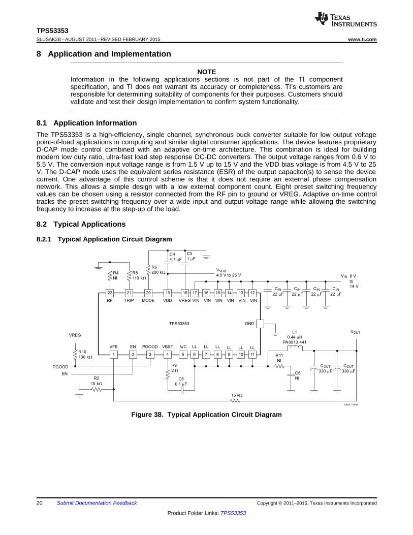
8.1 Application InformationThe TPS53353 is a high-efficiency, single channel, synchronous buck converter suitable for low output voltagepoint-of-load applications in computing and similar digital consumer applications. The device features proprietaryD-CAP mode control combined with an adaptive on-time architecture. This combination is ideal for buildingmodern low duty ratio, ultra-fast load step response DC-DC converters. The output voltage ranges from 0.6 V to5.5 V. The conversion input voltage range is from 1.5 V up to 15 V and the VDD bias voltage is from 4.5 V to 25V. The D-CAP mode uses the equivalent series resistance (ESR) of the output capacitor(s) to sense the devicecurrent. One advantage of this control scheme is that it does not require an external phase compensationnetwork. This allows a simple design with a low external component count. Eight preset switching frequencyvalues can be chosen using a resistor connected from the RF pin to ground or VREG. Adaptive on-time controltracks the preset switching frequency over a wide input and output voltage range while allowing the switchingfrequency to increase at the step-up of the load.
8.2 Typical Applications
8.2.1 Typical Application Circuit Diagram
Figure 38. Typical Application Circuit Diagram
20 Submit Documentation Feedback Copyright © 2011–2015, Texas Instruments Incorporated
Product Folder Links: TPS53353

( )( )
( )( )( )
- ´= + ´
´ ´
IN OUT OUTmaxTRIP
IND peakSW INDS on max
V V VV 1I
32 R L f V
( )
( )( )( ) ( )
( )( )- ´ - ´= ´ = ´
´ ´
IN OUT OUT IN OUT OUTmax max
SW IN OUT SW IN(max)IND ripple max max
V V V V V V1 3
LI f V I f V
TPS53353www.ti.com SLUSAK2B –AUGUST 2011–REVISED FEBRUARY 2015
Typical Applications (continued)8.2.1.1 Design Requirements
Table 4. Design ParametersPARAMETER TEST CONDITIONS MIN TYP MAX UNIT
INPUT CHARACTERISTICSVIN Voltage range 8 12 14 V
Maximum Input current VIN = 8 V, IOUT = 20 A 4.1 AIMAX No load input current VIN = 14 V, IOUT = 0 A with auto-skip mode 1 mAOUTPUT CHARACTERISTICS
Output voltage 1.5 VLine regulation, 8 V ≤ VIN ≤ 15 V 0.1%VOUT Output voltage regulation Load regulation, VIN = 12 V, 0 A ≤ IOUT ≤ 20 0.2%A with FCCM
VRIPPLE Output voltage ripple VIN = 12 V, IOUT = 20 A with FCCM 20 mVPP
ILOAD Output load current 0 20 AOutput overcurrentIOCP 26 Athreshold
tSS Soft-start time 1.4 msSYSTEMS CHARACTERISTICSfSW Switching frequency 500 kHz
Peak efficiency VIN = 12 V, VOUT = 1.1 V, IOUT = 10 A 91.87%η
Full load efficiency VIN = 12 V, VOUT = 1.1 V, IOUT = 20 A 91.38%TA Operating temperature 25 °C
8.2.1.2 Detailed Design Procedure
8.2.1.2.1 External Component Selection
Refer to the External Component Selection Using All Ceramic Output Capacitors section for guidelines for thisdesign with all ceramic output capacitors.
The external components selection is a simple process when using organic semiconductors or special polymeroutput capacitors.1. SELECT OPERATION MODE AND SOFT-START TIME
Select operation mode and soft-start time using Table 3.2. SELECT SWITCHING FREQUENCY
Select the switching frequency from 250 kHz to 1 MHz using Table 1.3. CHOOSE THE INDUCTOR
The inductance value should be determined to give the ripple current of approximately 1/4 to 1/2 of maximumoutput current. Larger ripple current increases output ripple voltage and improves signal-to-noise ratio andhelps ensure stable operation, but increases inductor core loss. Using 1/3 ripple current to maximum outputcurrent ratio, the inductance can be determined by Equation 8.
(8)
The inductor requires a low DCR to achieve good efficiency. It also requires enough room above peakinductor current before saturation. The peak inductor current can be estimated in Equation 9.
(9)
Copyright © 2011–2015, Texas Instruments Incorporated Submit Documentation Feedback 21
Product Folder Links: TPS53353

( ) ( )æ ö- ´æ ö
- ´ ´ ´ Wç ÷ç ÷ç ÷´ ´è øè øW =m
IN OUT OUTOCP DS(on)
SW INTRIP
TRIP
V V V1I 32 R m
2 L f VR (k )
I ( A)
( ) ´- -
= ´
IND ripple
OUT
I ESRV 0.6
2R1 R20.6
( )( )
´ ´ - ´ ´ ´= = = W
´
OUT SW SW
IND ripple
V 10mV (1 D) 10mV L f L fESR
0.6 V I 0.6 V 60
TPS53353SLUSAK2B –AUGUST 2011–REVISED FEBRUARY 2015 www.ti.com
4. CHOOSE THE OUTPUT CAPACITORS
When organic semiconductor capacitors or specialty polymer capacitors are used, for loop stability,capacitance and ESR should satisfy Equation 6. For jitter performance, Equation 10 is a good starting pointto determine ESR.
where• D is the duty factor.• The required output ripple slope is approximately 10 mV per tSW (switching period) in terms of VFB terminal
voltage. (10)5. DETERMINE THE VALUE OF R1 AND R2
The output voltage is programmed by the voltage-divider resistor, R1 and R2 shown in Figure 37. R1 isconnected between VFB pin and the output, and R2 is connected between the VFB pin and GND.Recommended R2 value is from 1 kΩ to 20 kΩ. Determine R1 using Equation 11.
(11)6. CHOOSE THE OVERCURRENT SETTING RESISTOR
The overcurrent setting resistor, RTRIP, can be determined by .
where• ITRIP is the TRIP pin sourcing current (10 µA).• RDS(on) is the thermally compensated on-time resistance value of the low-side MOSFET. (12)
Use an RDS(on) value of 1.6 mΩ for an overcurrent level of approximately 20 A. Use an RDS(on) value of1.7 mΩ for overcurrent level of approximately 10 A.
8.2.1.3 Application Curves
Figure 39. Enable Turnon Figure 40. Enable Turnoff
22 Submit Documentation Feedback Copyright © 2011–2015, Texas Instruments Incorporated
Product Folder Links: TPS53353

UDG-11050
RF TRIP MODE VDD VREG VIN VIN VIN VIN VINVIN
TPS53353
VFB EN PGOOD VBST N/C LL LL LL
1 2 3 4 5 6 7 8 9 10 11
22 21 20 19 18 17 16 15 14 13 12
VOUT
C5
0.1 mF
VREG
CIN
22 mF
GND
LL LL LL
L1
0.44 mH
PA0513.441
COUT
4 x 100 mF
Ceramic
R1 14.7kW
R2
10 kW
R10
100 kW
VIN
R11
NI
C6
NI
R9
2 W
CIN
22 mF
CIN
22 mF
CIN
22 mF
8 V
to
14 V
R6
200 kWR8
110 kW
R4
NI
C4
4.7 mF
C3
1 mF
VVDD
4.5 V to 25 V
R7
3.01 kW
C1
0.1 mF
C2
1 nF
EN
PGOOD
TPS53353www.ti.com SLUSAK2B –AUGUST 2011–REVISED FEBRUARY 2015
8.2.2 Typical Application Circuit Diagram With Ceramic Output Capacitors
Figure 41. Typical Application Circuit Diagram With Ceramic Output Capacitors
8.2.2.1 Design Requirements
Table 5. Design ParametersPARAMETER TEST CONDITIONS MIN TYP MAX UNIT
INPUT CHARACTERISTICSVIN Voltage range 8 12 14 V
Maximum Input current VIN = 8 V, IOUT = 20 A 4.1 AIMAX No load input current VIN = 14 V, IOUT = 0 A with auto-skip mode 1 mAOUTPUT CHARACTERISTICS
Output voltage 1.5 VLine regulation, 8 V ≤ VIN ≤ 15 V 0.1%VOUT Output voltage regulation Load regulation, VIN = 12 V, 0 A ≤ IOUT ≤ 20 0.2%A with FCCM
VRIPPLE Output voltage ripple VIN = 12 V, IOUT = 20 A with FCCM 20 mVPP
ILOAD Output load current 0 20 AOutput overcurrentIOCP 26 Athreshold
tSS Soft-start time 1.4 msSYSTEMS CHARACTERISTICSfSW Switching frequency 500 kHz
Peak efficiency VIN = 12 V, VOUT = 1.1 V, IOUT = 10 A 91.87%η
Full load efficiency VIN = 12 V, VOUT = 1.1 V, IOUT = 20 A 91.38%TA Operating temperature 25 °C
Copyright © 2011–2015, Texas Instruments Incorporated Submit Documentation Feedback 23
Product Folder Links: TPS53353
( ) ( )æ ö- ´æ ö
- ´ ´ ´ Wç ÷ç ÷ç ÷´ ´è øè øW =m
IN OUT OUTOCP DS(on)
SW INTRIP
TRIP
V V V1I 32 R m
2 L f VR (k )
I ( A)
( )( )
( )( )( )
- ´= + ´
´ ´
IN OUT OUTmaxTRIP
IND peakSW INDS on max
V V VV 1I
32 R L f V
( )
( )( )( ) ( )
( )( )- ´ - ´= ´ = ´
´ ´
IN OUT OUT IN OUT OUTmax max
SW IN OUT SW IN(max)IND ripple max max
V V V V V V1 3
LI f V I f V
TPS53353SLUSAK2B –AUGUST 2011–REVISED FEBRUARY 2015 www.ti.com
8.2.2.2 Detailed Design Procedure
8.2.2.2.1 External Component Selection
Refer to the External Component Selection Using All Ceramic Output Capacitors section for guidelines for thisdesign with all ceramic output capacitors.
The external components selection is a simple process when using organic semiconductors or special polymeroutput capacitors.1. SELECT OPERATION MODE AND SOFT-START TIME
Select operation mode and soft-start time using Table 3.2. SELECT SWITCHING FREQUENCY
Select the switching frequency from 250 kHz to 1 MHz using Table 1.3. CHOOSE THE INDUCTOR
The inductance value should be determined to give the ripple current of approximately 1/4 to 1/2 of maximumoutput current. Larger ripple current increases output ripple voltage and improves signal-to-noise ratio andhelps ensure stable operation, but increases inductor core loss. Using 1/3 ripple current to maximum outputcurrent ratio, the inductance can be determined by Equation 8.
(13)
The inductor requires a low DCR to achieve good efficiency. It also requires enough room above peakinductor current before saturation. The peak inductor current can be estimated in Equation 9.
(14)4. EXTERNAL COMPONENT SELECTION WITH ALL CERAMIC OUTPUT CAPACITORS
Refer to the External Component Selection Using All Ceramic Output Capacitors section to select externalcomponents because ceramic output capacitors are used in this design.
5. CHOOSE THE OVERCURRENT SETTING RESISTOR
The overcurrent setting resistor, RTRIP, can be determined by .
where• ITRIP is the TRIP pin sourcing current (10 µA).• RDS(on) is the thermally compensated on-time resistance value of the low-side MOSFET. (15)
Use an RDS(on) value of 1.6 mΩ for an overcurrent level of approximately 20 A. Use an RDS(on) value of1.7 mΩ for overcurrent level of approximately 10 A.
8.2.2.2.2 External Component Selection Using All Ceramic Output Capacitors
When a ceramic output capacitor is used, the stability criteria in Equation 6 cannot be satisfied. The rippleinjection approach as shown in Figure 41 is implemented to increase the ripple on the VFB pin and make thesystem stable. In addition to the selections made using Steps 1 through Step 6 in the section, the ripple injectioncomponents must be selected. The C2 value can be fixed at 1 nF. The value of C1 can be selected from 10 nFto 200 nF.
24 Submit Documentation Feedback Copyright © 2011–2015, Texas Instruments Incorporated
Product Folder Links: TPS53353

-
= ´OUT VFB
VFB
V VR1 R2
V
+
= +INJ_ SW INJ_ OUT
VFB
V VV 0.6
2
( )( )
= ´ +´ ´
IND ripple
INJ_ OUT IND rippleOUT SW
IV ESR I
8 C f
-
= ´
´
IN OUTINJ_ SW
SW
V V DV
R7 C1 f
´
> ´
´
OUT ONL C tN
R7 C1 2
TPS53353www.ti.com SLUSAK2B –AUGUST 2011–REVISED FEBRUARY 2015
where• N is the coefficient to account for L and COUT variation. (16)
N is also used to provide enough margin for stability. It is recommended N = 2 for VOUT ≤ 1.8 V and N = 4 forVOUT ≥ 3.3 V or when L ≤ 250 nH. The higher VOUT needs a higher N value because the effective outputcapacitance is reduced significantly with higher DC bias. For example, a 6.3-V, 22-µF ceramic capacitor mayhave only 8 µF of effective capacitance when biased at 5 V.
Because the VFB pin voltage is regulated at the valley, the increased ripple on the VFB pin causes the increaseof the VFB DC value. The AC ripple coupled to the VFB pin has two components, one coupled from SW nodeand the other coupled from the VOUT pin and they can be calculated using Equation 17 and Equation 18 whenneglecting the output voltage ripple caused by equivalent series inductance (ESL).
(17)
(18)
It is recommended that VINJ_SW to be less than 50 mV. If the calculated VINJ_SW is higher than 50 mV, then otherparameters must be adjusted to reduce it. For example, COUT can be increased to satisfy Equation 16 with ahigher R7 value, thereby reducing VINJ_SW.
The DC voltage at the VFB pin can be calculated by Equation 19:
(19)
And the resistor divider value can be determined by Equation 20:
(20)
8.2.2.3 Application Curves
Figure 42. Enable Turnon Figure 43. Enable Turnoff
Copyright © 2011–2015, Texas Instruments Incorporated Submit Documentation Feedback 25
Product Folder Links: TPS53353
TPS53353SLUSAK2B –AUGUST 2011–REVISED FEBRUARY 2015 www.ti.com
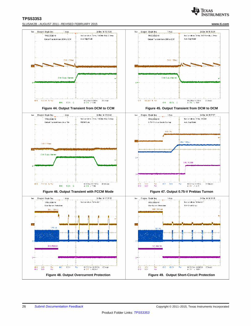
Figure 44. Output Transient from DCM to CCM Figure 45. Output Transient from DCM to DCM
Figure 46. Output Transient with FCCM Mode Figure 47. Output 0.75-V Prebias Turnon
Figure 48. Output Overcurrent Protection Figure 49. Output Short-Circuit Protection
26 Submit Documentation Feedback Copyright © 2011–2015, Texas Instruments Incorporated
Product Folder Links: TPS53353
TPS53353www.ti.com SLUSAK2B –AUGUST 2011–REVISED FEBRUARY 2015
9 Power Supply RecommendationsThe device is designed to operate from an input voltage supply range from 1.5 V to 22 V (4.5 V to 25 V biased).This input supply must be well regulated. Proper bypassing of input supplies and internal regulators is alsocritical for noise performance, as is PCB layout and grounding scheme. See the recommendations in the Layoutsection.
10 Layout
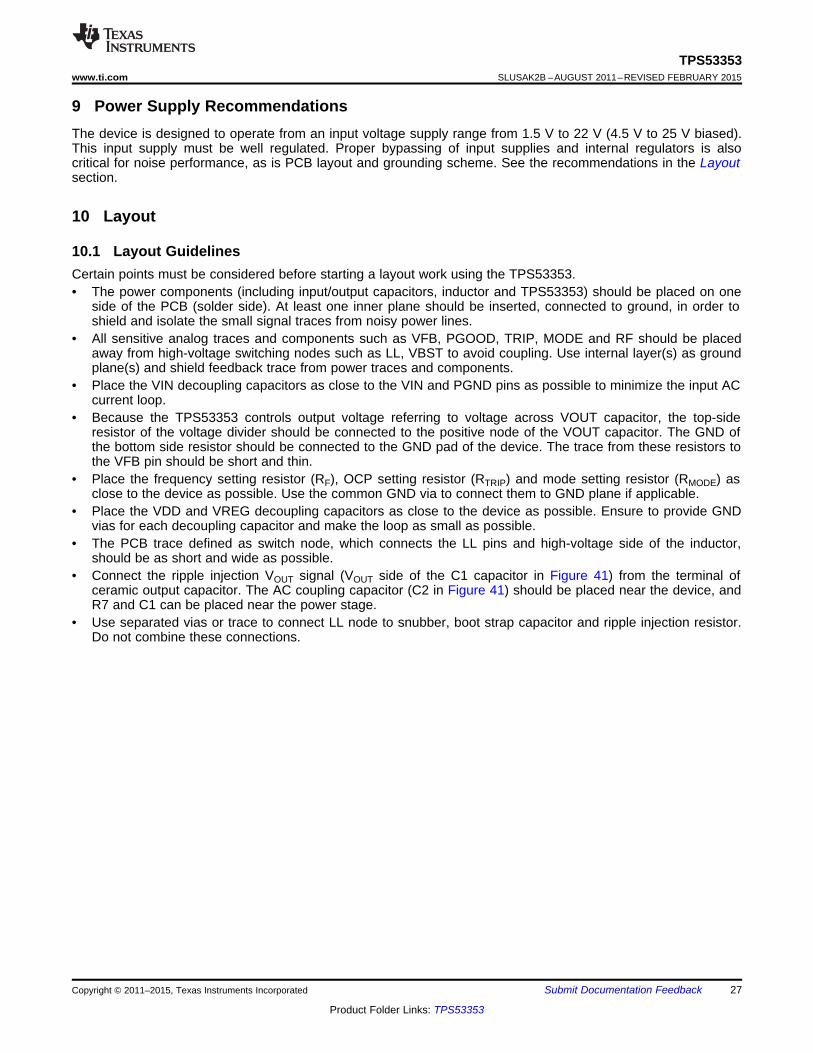
10.1 Layout GuidelinesCertain points must be considered before starting a layout work using the TPS53353.• The power components (including input/output capacitors, inductor and TPS53353) should be placed on one
side of the PCB (solder side). At least one inner plane should be inserted, connected to ground, in order toshield and isolate the small signal traces from noisy power lines.
• All sensitive analog traces and components such as VFB, PGOOD, TRIP, MODE and RF should be placedaway from high-voltage switching nodes such as LL, VBST to avoid coupling. Use internal layer(s) as groundplane(s) and shield feedback trace from power traces and components.
• Place the VIN decoupling capacitors as close to the VIN and PGND pins as possible to minimize the input ACcurrent loop.
• Because the TPS53353 controls output voltage referring to voltage across VOUT capacitor, the top-sideresistor of the voltage divider should be connected to the positive node of the VOUT capacitor. The GND ofthe bottom side resistor should be connected to the GND pad of the device. The trace from these resistors tothe VFB pin should be short and thin.
• Place the frequency setting resistor (RF), OCP setting resistor (RTRIP) and mode setting resistor (RMODE) asclose to the device as possible. Use the common GND via to connect them to GND plane if applicable.
• Place the VDD and VREG decoupling capacitors as close to the device as possible. Ensure to provide GNDvias for each decoupling capacitor and make the loop as small as possible.
• The PCB trace defined as switch node, which connects the LL pins and high-voltage side of the inductor,should be as short and wide as possible.
• Connect the ripple injection VOUT signal (VOUT side of the C1 capacitor in Figure 41) from the terminal ofceramic output capacitor. The AC coupling capacitor (C2 in Figure 41) should be placed near the device, andR7 and C1 can be placed near the power stage.
• Use separated vias or trace to connect LL node to snubber, boot strap capacitor and ripple injection resistor.Do not combine these connections.
Copyright © 2011–2015, Texas Instruments Incorporated Submit Documentation Feedback 27
Product Folder Links: TPS53353
To GND Plane
Bottom side
components and trace
Bottom side
component
and trace
GND shape
Keep VFB trace short and
away from noisy signals
VIN shapeVOUT shape
LL shape
RF
TR
IP
MO
DE
VD
D VREG
PGOOD
EN
VFB
VOUT
GND
Bottom side
components and trace
VBST
UDG-11166
TPS53353SLUSAK2B –AUGUST 2011–REVISED FEBRUARY 2015 www.ti.com
10.2 Layout Example
Figure 50. Layout Recommendation
28 Submit Documentation Feedback Copyright © 2011–2015, Texas Instruments Incorporated
Product Folder Links: TPS53353
TPS53353www.ti.com SLUSAK2B –AUGUST 2011–REVISED FEBRUARY 2015
11 Device and Documentation Support
11.1 TrademarksEco-mode, NexFET, PowerPAD are trademarks of Texas Instruments.All other trademarks are the property of their respective owners.
11.2 Electrostatic Discharge CautionThese devices have limited built-in ESD protection. The leads should be shorted together or the device placed in conductive foamduring storage or handling to prevent electrostatic damage to the MOS gates.
11.3 GlossarySLYZ022 — TI Glossary.
This glossary lists and explains terms, acronyms, and definitions.
12 Mechanical, Packaging, and Orderable InformationThe following pages include mechanical, packaging, and orderable information. This information is the mostcurrent data available for the designated devices. This data is subject to change without notice and revision ofthis document. For browser-based versions of this data sheet, refer to the left-hand navigation.
Copyright © 2011–2015, Texas Instruments Incorporated Submit Documentation Feedback 29
Product Folder Links: TPS53353
PACKAGE OPTION ADDENDUM
www.ti.com 9-Sep-2014
Addendum-Page 1
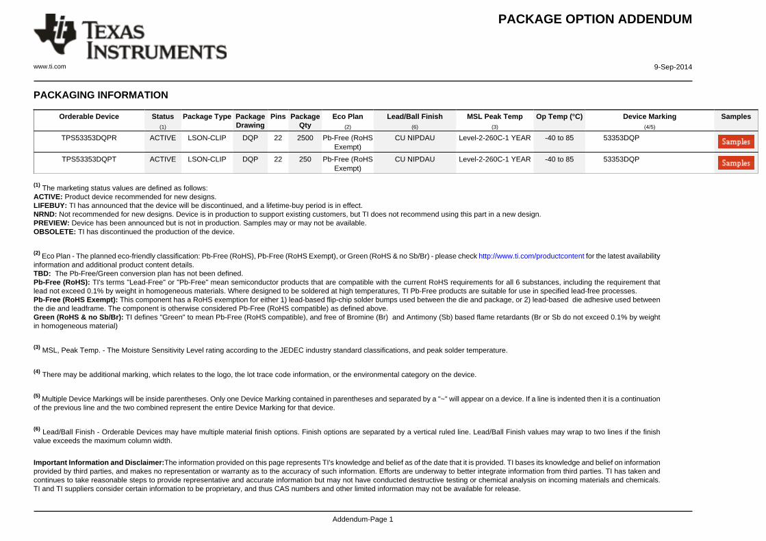
PACKAGING INFORMATION
Orderable Device Status(1)
Package Type PackageDrawing
Pins PackageQty
Eco Plan(2)
Lead/Ball Finish(6)
MSL Peak Temp(3)
Op Temp (°C) Device Marking(4/5)
Samples
TPS53353DQPR ACTIVE LSON-CLIP DQP 22 2500 Pb-Free (RoHSExempt)
CU NIPDAU Level-2-260C-1 YEAR -40 to 85 53353DQP
TPS53353DQPT ACTIVE LSON-CLIP DQP 22 250 Pb-Free (RoHSExempt)
CU NIPDAU Level-2-260C-1 YEAR -40 to 85 53353DQP
(1) The marketing status values are defined as follows:ACTIVE: Product device recommended for new designs.LIFEBUY: TI has announced that the device will be discontinued, and a lifetime-buy period is in effect.NRND: Not recommended for new designs. Device is in production to support existing customers, but TI does not recommend using this part in a new design.PREVIEW: Device has been announced but is not in production. Samples may or may not be available.OBSOLETE: TI has discontinued the production of the device.
(2) Eco Plan - The planned eco-friendly classification: Pb-Free (RoHS), Pb-Free (RoHS Exempt), or Green (RoHS & no Sb/Br) - please check http://www.ti.com/productcontent for the latest availabilityinformation and additional product content details.TBD: The Pb-Free/Green conversion plan has not been defined.Pb-Free (RoHS): TI's terms "Lead-Free" or "Pb-Free" mean semiconductor products that are compatible with the current RoHS requirements for all 6 substances, including the requirement thatlead not exceed 0.1% by weight in homogeneous materials. Where designed to be soldered at high temperatures, TI Pb-Free products are suitable for use in specified lead-free processes.Pb-Free (RoHS Exempt): This component has a RoHS exemption for either 1) lead-based flip-chip solder bumps used between the die and package, or 2) lead-based die adhesive used betweenthe die and leadframe. The component is otherwise considered Pb-Free (RoHS compatible) as defined above.Green (RoHS & no Sb/Br): TI defines "Green" to mean Pb-Free (RoHS compatible), and free of Bromine (Br) and Antimony (Sb) based flame retardants (Br or Sb do not exceed 0.1% by weightin homogeneous material)
(3) MSL, Peak Temp. - The Moisture Sensitivity Level rating according to the JEDEC industry standard classifications, and peak solder temperature.
(4) There may be additional marking, which relates to the logo, the lot trace code information, or the environmental category on the device.
(5) Multiple Device Markings will be inside parentheses. Only one Device Marking contained in parentheses and separated by a "~" will appear on a device. If a line is indented then it is a continuationof the previous line and the two combined represent the entire Device Marking for that device.
(6) Lead/Ball Finish - Orderable Devices may have multiple material finish options. Finish options are separated by a vertical ruled line. Lead/Ball Finish values may wrap to two lines if the finishvalue exceeds the maximum column width.
Important Information and Disclaimer:The information provided on this page represents TI's knowledge and belief as of the date that it is provided. TI bases its knowledge and belief on informationprovided by third parties, and makes no representation or warranty as to the accuracy of such information. Efforts are underway to better integrate information from third parties. TI has taken andcontinues to take reasonable steps to provide representative and accurate information but may not have conducted destructive testing or chemical analysis on incoming materials and chemicals.TI and TI suppliers consider certain information to be proprietary, and thus CAS numbers and other limited information may not be available for release.

PACKAGE OPTION ADDENDUM
www.ti.com 9-Sep-2014
Addendum-Page 2
In no event shall TI's liability arising out of such information exceed the total purchase price of the TI part(s) at issue in this document sold by TI to Customer on an annual basis.
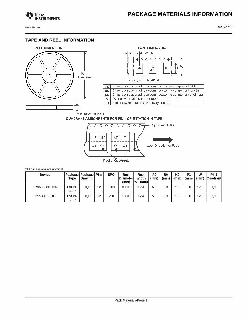
TAPE AND REEL INFORMATION
*All dimensions are nominal
Device PackageType
PackageDrawing
Pins SPQ ReelDiameter
(mm)
ReelWidth
W1 (mm)
A0(mm)
B0(mm)
K0(mm)
P1(mm)
W(mm)
Pin1Quadrant
TPS53353DQPR LSON-CLIP
DQP 22 2500 330.0 12.4 5.3 6.3 1.8 8.0 12.0 Q1
TPS53353DQPT LSON-CLIP
DQP 22 250 180.0 12.4 5.3 6.3 1.8 8.0 12.0 Q1
PACKAGE MATERIALS INFORMATION
www.ti.com 15-Apr-2014
Pack Materials-Page 1
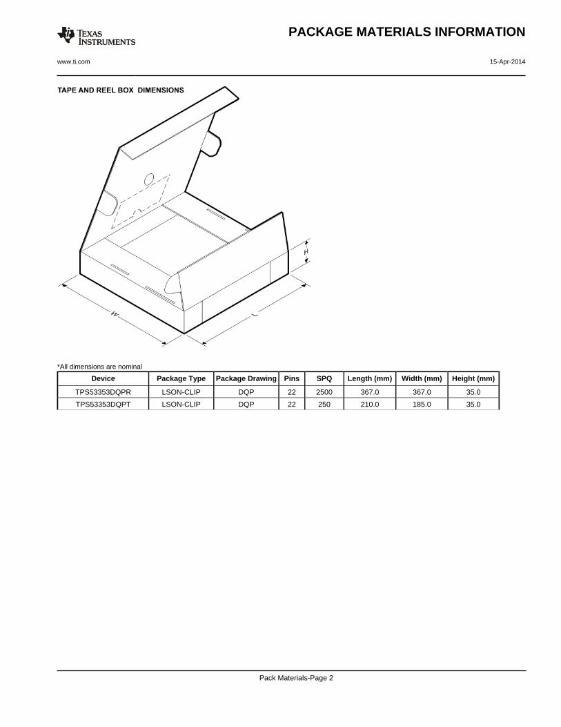
*All dimensions are nominal
Device Package Type Package Drawing Pins SPQ Length (mm) Width (mm) Height (mm)
TPS53353DQPR LSON-CLIP DQP 22 2500 367.0 367.0 35.0
TPS53353DQPT LSON-CLIP DQP 22 250 210.0 185.0 35.0
PACKAGE MATERIALS INFORMATION
www.ti.com 15-Apr-2014
Pack Materials-Page 2
IMPORTANT NOTICE
Texas Instruments Incorporated and its subsidiaries (TI) reserve the right to make corrections, enhancements, improvements and otherchanges to its semiconductor products and services per JESD46, latest issue, and to discontinue any product or service per JESD48, latestissue. Buyers should obtain the latest relevant information before placing orders and should verify that such information is current andcomplete. All semiconductor products (also referred to herein as “components”) are sold subject to TI’s terms and conditions of salesupplied at the time of order acknowledgment.TI warrants performance of its components to the specifications applicable at the time of sale, in accordance with the warranty in TI’s termsand conditions of sale of semiconductor products. Testing and other quality control techniques are used to the extent TI deems necessaryto support this warranty. Except where mandated by applicable law, testing of all parameters of each component is not necessarilyperformed.TI assumes no liability for applications assistance or the design of Buyers’ products. Buyers are responsible for their products andapplications using TI components. To minimize the risks associated with Buyers’ products and applications, Buyers should provideadequate design and operating safeguards.TI does not warrant or represent that any license, either express or implied, is granted under any patent right, copyright, mask work right, orother intellectual property right relating to any combination, machine, or process in which TI components or services are used. Informationpublished by TI regarding third-party products or services does not constitute a license to use such products or services or a warranty orendorsement thereof. Use of such information may require a license from a third party under the patents or other intellectual property of thethird party, or a license from TI under the patents or other intellectual property of TI.Reproduction of significant portions of TI information in TI data books or data sheets is permissible only if reproduction is without alterationand is accompanied by all associated warranties, conditions, limitations, and notices. TI is not responsible or liable for such altereddocumentation. Information of third parties may be subject to additional restrictions.Resale of TI components or services with statements different from or beyond the parameters stated by TI for that component or servicevoids all express and any implied warranties for the associated TI component or service and is an unfair and deceptive business practice.TI is not responsible or liable for any such statements.Buyer acknowledges and agrees that it is solely responsible for compliance with all legal, regulatory and safety-related requirementsconcerning its products, and any use of TI components in its applications, notwithstanding any applications-related information or supportthat may be provided by TI. Buyer represents and agrees that it has all the necessary expertise to create and implement safeguards whichanticipate dangerous consequences of failures, monitor failures and their consequences, lessen the likelihood of failures that might causeharm and take appropriate remedial actions. Buyer will fully indemnify TI and its representatives against any damages arising out of the useof any TI components in safety-critical applications.In some cases, TI components may be promoted specifically to facilitate safety-related applications. With such components, TI’s goal is tohelp enable customers to design and create their own end-product solutions that meet applicable functional safety standards andrequirements. Nonetheless, such components are subject to these terms.No TI components are authorized for use in FDA Class III (or similar life-critical medical equipment) unless authorized officers of the partieshave executed a special agreement specifically governing such use.Only those TI components which TI has specifically designated as military grade or “enhanced plastic” are designed and intended for use inmilitary/aerospace applications or environments. Buyer acknowledges and agrees that any military or aerospace use of TI componentswhich have not been so designated is solely at the Buyer's risk, and that Buyer is solely responsible for compliance with all legal andregulatory requirements in connection with such use.TI has specifically designated certain components as meeting ISO/TS16949 requirements, mainly for automotive use. In any case of use ofnon-designated products, TI will not be responsible for any failure to meet ISO/TS16949.
Products ApplicationsAudio www.ti.com/audio Automotive and Transportation www.ti.com/automotiveAmplifiers amplifier.ti.com Communications and Telecom www.ti.com/communicationsData Converters dataconverter.ti.com Computers and Peripherals www.ti.com/computersDLP® Products www.dlp.com Consumer Electronics www.ti.com/consumer-appsDSP dsp.ti.com Energy and Lighting www.ti.com/energyClocks and Timers www.ti.com/clocks Industrial www.ti.com/industrialInterface interface.ti.com Medical www.ti.com/medicalLogic logic.ti.com Security www.ti.com/securityPower Mgmt power.ti.com Space, Avionics and Defense www.ti.com/space-avionics-defenseMicrocontrollers microcontroller.ti.com Video and Imaging www.ti.com/videoRFID www.ti-rfid.comOMAP Applications Processors www.ti.com/omap TI E2E Community e2e.ti.comWireless Connectivity www.ti.com/wirelessconnectivity
Mailing Address: Texas Instruments, Post Office Box 655303, Dallas, Texas 75265Copyright © 2015, Texas Instruments Incorporated
Mouser Electronics
Authorized Distributor
Click to View Pricing, Inventory, Delivery & Lifecycle Information: Texas Instruments:
TPS53353DQPR TPS53353DQPT