High contrast modulation of plasmonic signals …juh17:publication:... · High contrast modulation...
10
High contrast modulation of plasmonic signals using nanoscale dual-frequency liquid crystals Joseph S. T. Smalley, 1 Yanhui Zhao, 1 Ahmad Ahsan Nawaz, 1 Qingzhen Hao, 1 Yi Ma, 2 Iam-Choon Khoo, 2 and Tony Jun Huang 1,* 1 Department of Engineering Science and Mechanics, Pennsylvania State University, University Park, PA 16802, USA 2 Department of Electrical Engineering, Pennsylvania State University, University Park, PA 16802, USA *[email protected] Abstract: We have designed and simulated a dual-frequency liquid crystal (DFLC) based plasmonic signal modulator capable of achieving over 15 dB modulation depth. The voltage-controlled DFLC is combined with a groove and slit configuration and its operation is discussed. Using the finite- difference time domain (FDTD) method, simulations were conducted to discover the groove-slit separation distance that enabled a practically useful modulation depth for the two states of the DFLC. Moreover, we have shown that significant improvement in modulation depth can be achieved by addition of a second groove to the design structure. Additionally, a performance analysis indicates a switching energy on the order of femtojoules and a switching speed on the order of 100 microseconds. Results of this investigation can be useful for the future design, simulation, and fabrication of DFLC-based plasmonic signal modulating devices, which have application in electro-optical and all-optical information systems. ©2011 Optical Society of America OCIS codes: (230.4110) Modulators; (250.5403) Plasmonics; (240.6680) Surface plasmons; (050.6624) Subwavelength structures. References and links 1. S. Bozhevolnyi, Plasmonic Nanoguides and Circuits (Pan Stanford Publishing: Singapore, 2009). 2. P. Berini, “Long-range surface plasmon polaritons,” Adv. Opt. Photon 1(3), 484–588 (2009). 3. N. Zheludev and K. MacDonald, “Active plasmonics: current status,” Laser Photon. Rev. 4, 527–532 (2010). 4. J. Dionne, L. Sweatlock, M. Sheldon, P. Alivisatos, and H. Atwater, “Silicon-based plasmonics for on-chip applications,” IEEE J. Select. Top. Quantum Electron. 16, 295–306 (2010). 5. Y. Zhao, S. C. Lin, A. A. Nawaz, B. Kiraly, Q. Hao, Y. Liu, and T. J. Huang, “Beam bending via plasmonic lenses,” Opt. Express 18(22), 23458–23465 (2010). 6. Y. B. Zheng, L. Jensen, W. Yan, T. R. Walker, B. K. Juluri, L. Jensen, and T. J. Huang, “Chemically Tuning the Localized Surface Plasmon Resonances of Gold Nanostructure Arrays,” J. Phys. Chem. C 113(17), 7019–7024 (2009). 7. Y. Zheng, T. J. Huang, A. Y. Desai, S. J. Wang, L. K. Tan, H. Gao, and A. C. H. Huan, “Thermal Behavior of Localized Surface Plasmon Resonance of Au/TiO2 Core/Shell Nanoparticle Arrays,” Appl. Phys. Lett. 90(18), 183117 (2007). 8. J. A. Dionne, K. Diest, L. A. Sweatlock, and H. A. Atwater, “PlasMOStor: a metal-oxide-Si field effect plasmonic modulator,” Nano Lett. 9(2), 897–902 (2009). 9. M. J. Dicken, L. A. Sweatlock, D. Pacifici, H. J. Lezec, K. Bhattacharya, and H. A. Atwater, “Electrooptic modulation in thin film barium titanate plasmonic interferometers,” Nano Lett. 8(11), 4048–4052 (2008). 10. W. Cai, J. S. White, and M. L. Brongersma, “Compact, high-speed and power-efficient electrooptic plasmonic modulators,” Nano Lett. 9(12), 4403–4411 (2009). 11. R. A. Pala, K. T. Shimizu, N. A. Melosh, and M. L. Brongersma, “A nonvolatile plasmonic switch employing photochromic molecules,” Nano Lett. 8(5), 1506–1510 (2008). 12. A. Y. Elezzabi, Z. Han, S. Sederberg, and V. Van, “Ultrafast all-optical modulation in silicon-based nanoplasmonic devices,” Opt. Express 17(13), 11045–11056 (2009). 13. D. Pacifici, H. Lezec, and H. Atwater, “All-optical modulation by plasmonic excitation of CdSe quantum dots,” Nat. Photonics 1(7), 402–406 (2007). 14. A. Krasavin and N. Zheludev, “Active plasmonics: controlling signals in Au/Ga waveguide using nanoscale structural transformations,” Appl. Phys. Lett. 84(8), 1416–1418 (2004). 15. A. Krasavin, K. MacDonald, N. Zheludev, and A. Zayats, “High-contrast modulation of light with light by control of surface plasmon polariton wave coupling,” Appl. Phys. Lett. 85(16), 3369–3371 (2004). #149816 - $15.00 USD Received 23 Jun 2011; revised 19 Jul 2011; accepted 20 Jul 2011; published 25 Jul 2011 (C) 2011 OSA 1 August 2011 / Vol. 19, No. 16 / OPTICS EXPRESS 15265
Transcript of High contrast modulation of plasmonic signals …juh17:publication:... · High contrast modulation...

High contrast modulation of plasmonic signals using nanoscale dual-frequency liquid crystals
Joseph S. T. Smalley,1 Yanhui Zhao,
1 Ahmad Ahsan Nawaz,
1 Qingzhen Hao,
1 Yi Ma,
2
Iam-Choon Khoo,2 and Tony Jun Huang
1,*
1 Department of Engineering Science and Mechanics, Pennsylvania State University, University Park, PA 16802, USA
2 Department of Electrical Engineering, Pennsylvania State University, University Park, PA 16802, USA *[email protected]
Abstract: We have designed and simulated a dual-frequency liquid crystal (DFLC) based plasmonic signal modulator capable of achieving over 15 dB modulation depth. The voltage-controlled DFLC is combined with a groove and slit configuration and its operation is discussed. Using the finite-difference time domain (FDTD) method, simulations were conducted to discover the groove-slit separation distance that enabled a practically useful modulation depth for the two states of the DFLC. Moreover, we have shown that significant improvement in modulation depth can be achieved by addition of a second groove to the design structure. Additionally, a performance analysis indicates a switching energy on the order of femtojoules and a switching speed on the order of 100 microseconds. Results of this investigation can be useful for the future design, simulation, and fabrication of DFLC-based plasmonic signal modulating devices, which have application in electro-optical and all-optical information systems.
©2011 Optical Society of America
OCIS codes: (230.4110) Modulators; (250.5403) Plasmonics; (240.6680) Surface plasmons; (050.6624) Subwavelength structures.
References and links
1. S. Bozhevolnyi, Plasmonic Nanoguides and Circuits (Pan Stanford Publishing: Singapore, 2009). 2. P. Berini, “Long-range surface plasmon polaritons,” Adv. Opt. Photon 1(3), 484–588 (2009). 3. N. Zheludev and K. MacDonald, “Active plasmonics: current status,” Laser Photon. Rev. 4, 527–532 (2010). 4. J. Dionne, L. Sweatlock, M. Sheldon, P. Alivisatos, and H. Atwater, “Silicon-based plasmonics for on-chip
applications,” IEEE J. Select. Top. Quantum Electron. 16, 295–306 (2010). 5. Y. Zhao, S. C. Lin, A. A. Nawaz, B. Kiraly, Q. Hao, Y. Liu, and T. J. Huang, “Beam bending via plasmonic
lenses,” Opt. Express 18(22), 23458–23465 (2010). 6. Y. B. Zheng, L. Jensen, W. Yan, T. R. Walker, B. K. Juluri, L. Jensen, and T. J. Huang, “Chemically Tuning the
Localized Surface Plasmon Resonances of Gold Nanostructure Arrays,” J. Phys. Chem. C 113(17), 7019–7024 (2009).
7. Y. Zheng, T. J. Huang, A. Y. Desai, S. J. Wang, L. K. Tan, H. Gao, and A. C. H. Huan, “Thermal Behavior of Localized Surface Plasmon Resonance of Au/TiO2 Core/Shell Nanoparticle Arrays,” Appl. Phys. Lett. 90(18), 183117 (2007).
8. J. A. Dionne, K. Diest, L. A. Sweatlock, and H. A. Atwater, “PlasMOStor: a metal-oxide-Si field effect plasmonic modulator,” Nano Lett. 9(2), 897–902 (2009).
9. M. J. Dicken, L. A. Sweatlock, D. Pacifici, H. J. Lezec, K. Bhattacharya, and H. A. Atwater, “Electrooptic modulation in thin film barium titanate plasmonic interferometers,” Nano Lett. 8(11), 4048–4052 (2008).
10. W. Cai, J. S. White, and M. L. Brongersma, “Compact, high-speed and power-efficient electrooptic plasmonic modulators,” Nano Lett. 9(12), 4403–4411 (2009).
11. R. A. Pala, K. T. Shimizu, N. A. Melosh, and M. L. Brongersma, “A nonvolatile plasmonic switch employing photochromic molecules,” Nano Lett. 8(5), 1506–1510 (2008).
12. A. Y. Elezzabi, Z. Han, S. Sederberg, and V. Van, “Ultrafast all-optical modulation in silicon-based nanoplasmonic devices,” Opt. Express 17(13), 11045–11056 (2009).
13. D. Pacifici, H. Lezec, and H. Atwater, “All-optical modulation by plasmonic excitation of CdSe quantum dots,” Nat. Photonics 1(7), 402–406 (2007).
14. A. Krasavin and N. Zheludev, “Active plasmonics: controlling signals in Au/Ga waveguide using nanoscale structural transformations,” Appl. Phys. Lett. 84(8), 1416–1418 (2004).
15. A. Krasavin, K. MacDonald, N. Zheludev, and A. Zayats, “High-contrast modulation of light with light by control of surface plasmon polariton wave coupling,” Appl. Phys. Lett. 85(16), 3369–3371 (2004).
#149816 - $15.00 USD Received 23 Jun 2011; revised 19 Jul 2011; accepted 20 Jul 2011; published 25 Jul 2011(C) 2011 OSA 1 August 2011 / Vol. 19, No. 16 / OPTICS EXPRESS 15265

16. G. Gagnon, N. Lahoud, G. Mattiussi, and P. Berini, “Thermally activated variable attenuation of a long-range surface plasmon-polaritons waves,” J. Lightwave Technol. 24(11), 4391–4402 (2006).
17. Y. B. Zheng, Y. W. Yang, L. Jensen, L. Fang, B. K. Juluri, A. H. Flood, P. S. Weiss, J. F. Stoddart, and T. J. Huang, “Active molecular plasmonics: controlling plasmon resonances with molecular switches,” Nano Lett. 9(2), 819–825 (2009).
18. N. Collings, W. A. Crossland, P. J. Ayliffe, D. G. Vass, and I. Underwood, “Evolutionary development of advanced liquid crystal spatial light modulators,” Appl. Opt. 28(22), 4740–4747 (1989).
19. E. Konshina, M. Fedorov, L. Amosova, M. Isaev, and D. Kostomarov, “Optical modulators based on a dual-frequency nematic liquid crystal,” J. Opt. Tech. 75(10), 670–675 (2008).
20. H. Huang, C. Wen, and S. Wu, “Polarization-independent and submillisecond response phase modulators using a 90 degrees twisted dual frequency liquid crystal,” Appl. Phys. Lett. 89(2), 021103 (2006).
21. I. C. Khoo, “Nonlinear Optics of Liquid Crystalline Materials,” Phys. Rep. 471(5-6), 221–267 (2009). 22. F. Simoni, Nonlinear Optical Properties of Liquid Crystals and Polymer Dispersed Liquid Crystals (World
Scientific: Singapore) 1997. 23. H. Xianya and C. Lin, “Dual frequency liquid crystals: a review,” Liquid Crystals 36(6-7), 717–726 (2009). 24. S. T. Wu and U. Efron, “Optical properties of thin nematic liquid crystal cells,” Appl. Phys. Lett. 48(10), 624–
626 (1986). 25. Q. Hao, Y. Zhao, B. K. Juluri, B. Kiraly, J. Liou, I. C. Khoo, and T. J. Huang, “Frequency-addressed tunable
transmission in optically thin metallic nanohole arrays with dual-frequency liquid crystals,” J. Appl. Phys. 109(8), 084340 (2011).
26. J. G. Cuennet, A. E. Vasdekis, L. De Sio, and D. Psaltis, “Optofluidic modulator based on peristaltic nematogen microflows,” Nat. Photonics 5(4), 234–238 (2011).
27. T. Bunning, L. V. Natarajan, V. P. Tondiglia, and R. L. Sutherland, “Holographic polymer-dispersed liquid crystals (H-PDLCs),” Annu. Rev. Mater. Sci. 30(1), 83–115 (2000).
28. H. Raether, Surface Plasmons on Smooth and Rough Surfaces and on Gratings (Spring-Verlag: New York, 1988)
29. Y. H. Fan, H. Ren, X. Liang, Y. H. Lin, and S. T. Wu, “Dual-frequency liquid crystal gels with sub-millisecond response time,” Appl. Phys. Lett. 85(13), 2451 (2004).
30. C. H. Wen and S. T. Wu, “Dielectric heating effects of dual-frequency liquid crystals,” Appl. Phys. Lett. 86(23), 231104 (2005).
31. E. Graugnard, S. N. Dunham, J. S. King, D. Lorang, S. Jain, and C. J. Summers, “Enhanced tunable Bragg diffraction in large-pore inverse opals using dual-frequency liquid crystal,” Appl. Phys. Lett. 91(11), 111101 (2007).
32. E. Graugnard, J. S. King, S. Jain, C. J. Summers, Y. Zhang-Williams, and I. C. Khoo, “Electric-field tuning of the Bragg peak in large-pore TiO2 inverse shell opals,” Phys. Rev. B 72(23), 233105 (2005).
33. O. Pishnyak, S. Sato, and O. D. Lavrentovich, “Electrically tunable lens based on a dual-frequency nematic liquid crystal,” Appl. Opt. 45(19), 4576–4582 (2006).
34. P. Yeh and C. Gu, Optics of Liquid Crystal Displays (Wiley: Hoboken, NJ, 2010). 35. Y. Liu, Q. Hao, J. Smalley, J. Liou, I. Khoo, and T. Huang, “A frequency-addressed plasmonic switch using
dual-frequency liquid crystals,” Appl. Phys. Lett. 97, 9 (2010). 36. H. Shi, C. Wang, C. Du, X. Luo, X. Dong, and H. Gao, “Beam manipulating by metallic nano-slits with variant
widths,” Opt. Express 13(18), 6815–6820 (2005). 37. OptiFDTD by Optiwave Corp., ver. 8.0, http://www.optiwave.com/ 38. E. Palik, Handbook of Optical Constants of Solids (Academic Press: San Diego, 1991). 39. I. I. Smolyaninov, Y. J. Hung, and C. C. Davis, “Magnifying superlens in the visible frequency range,” Science
315(5819), 1699–1701 (2007).
Introduction
Plasmonic device research has emerged aggressively as the need to combine electronic and photonic systems has become more acute [1,2]. Essential to future plasmonic circuits and systems is a means of reliable, scalable and energy efficient signal modulation [3–7]. Concepts for achieving modulation have focused on using an active material whose properties can be changed by some form of stimulation. The speed of operation, energy consumption, modulation depth, device footprint, reliability, and cost are, in general, all determined by the choice of this material-stimulant combination. Static electric fields in combination with doped semiconducting thin films [8], oxides [9, 10], and photochromic molecules [11]; laser beams in combination with metal-semiconductor waveguides [12], quantum dots [13], and phase-changing materials [14,15]; electric currents used for thermal activation of semiconductors [16]; and rotaxanes in combination with charged species [17] have all been demonstrated. As noted in [12], the limitations on modulator performance tend to result from the means of stimulation. For example, modulation by a static electric field is constrained by capacitance and thermal stimulation is constrained by thermal diffusivity.
#149816 - $15.00 USD Received 23 Jun 2011; revised 19 Jul 2011; accepted 20 Jul 2011; published 25 Jul 2011(C) 2011 OSA 1 August 2011 / Vol. 19, No. 16 / OPTICS EXPRESS 15266

Liquid crystals can serve as excellent active nanomaterials for plasmonic modulators, due to their large and controllable birefringence. In addition, they offer reliability, robustness, long lifetime, and low costs [18–25]. While the response time of liquid crystals is usually long, causing the efficiencies of modulators that employ liquid crystals to be low, the response time does decrease with cell thickness. Furthermore, new concepts, like polymer-stabilized liquid crystals, and flow effects in microfluidic structures, have been proposed to further decrease the response time [26, 27]. In this work, we demonstrate the feasibility of nanoscale, high-contrast modulation of surface plasmon polaritons (SPP) propagating along an interface between silver and dual-frequency liquid crystals (DFLC). Our results indicate that the proposed DFLC-based plasmonic modulation can achieve over 15 dB modulation depth with femtojoule activation energy. The ultimate speed of modulation is limited by the sub-micron thick nematic layer, which is on the order of 100 microseconds.
Principles and design
Figure 1 shows the schematic of the DFLC-based nanoplasmonic modulator. Such DFLCs can change the sign of dielectric anisotropy either from positive to negative, or from negative to positive, when the frequency of the applied field changes. A groove-slit geometry defines the basis of the design. The operating principles of our DFLC-enabled nanoplasmonic modulator consist of (1) SPP excitation by diffraction through a slit on silver film; (2) phase modulation of SPP signal by electro-optic DFLC; and (3) interference of SPP signal produced by input beam with optical pump beam at the slit. In other words, the input optical beam at the groove excites a SPP that propagates over a region embedded with DFLC. Then, the pump beam interferes with the SPP at the slit and the output intensity is measured at an observation point. Contrast between output signals is achieved by varying the dielectric anisotropy of the DFLC, which is accomplished through an applied voltage. Our investigation is focused on measuring the output as a function of groove-slit separation distance.
Fig. 1. Schematic of the DFLC-based nanoplasmonic modulator. An SPP is excited through diffraction-mediated transfer of momentum from the input. The SPP wave (shown here in pink) then propagates through the DFLCs, which exhibits either an ordinary or extraordinary refractive index, depending on the frequency of an applied voltage. Thus, the signal enters the interference stage at a phase that is dependent on the path length traveled and refractive index of the DFLC. Finally, a pump beam creates an interference pattern with the plasmonic signal, which is read as output information.
The conversion of propagating electromagnetic (EM) waves into SPP waves is achieved through the matching of the momentum of the two waves. In our case, we use a groove with sharp edges to diffract the incident EM waves to generate SPP waves. The wave vector of the
#149816 - $15.00 USD Received 23 Jun 2011; revised 19 Jul 2011; accepted 20 Jul 2011; published 25 Jul 2011(C) 2011 OSA 1 August 2011 / Vol. 19, No. 16 / OPTICS EXPRESS 15267

generated SPP modes is determined by the permittivity of the metal and dielectric, following the equation [28]
0
,m d
spp
m d
k kε εε ε
=+
(1)
where εm denotes the permittivity of the metal, εd represents the permittivity of the dielectric, and k0 and kspp are wave vectors of the incident EM and SPP waves, respectively. Based on Eq. (1) and the relation n
2 = ε for non-magnetic materials, where n is the refractive index, we
can see that the SPP wave vector changes with the refractive index. In this work, the dielectric material is DFLC [29–34]. This DFLC material, such as MLC-
2048(Merck) used in Ref [35]. has a positive sign of dielectric anisotropy||
0ε ε ε⊥∆ = − > ,
for frequencies f of the applied electric field smaller than the crossover frequency fc and has a
negative sign, 0ε∆ < , when f > fc. Here ||ε and ε⊥ are the dielectric permittivities of the
DFLCs in the directions parallel and perpendicular to the LC director, respectively. For LCs
with 0ε∆ > , the director prefers to align toward the electric field direction, then the light
wave travelling through LCs will see an ordinary refractive index denoted as no; while for
0ε∆ < , LC realign perpendicularly to the field, and the light waves see an extraordinary
refractive index, denoted as ne. If an SPP wave propagates through the LC with no, and a second wave excited by the
same light source at a later time travels through the LC with ne, the two waves will have a phase difference with respect to each other by an amount that depends on the SPP wavelength, the length of the LC cell, and ∆n ( = ne - no). Because the two waves have a phase difference, their interaction with a pump beam will generate two distinct transmission signals. The phase modulation of the DFLC can be designed such that the transmission signals achieve a desired contrast that can be observed in the output signals. For applications in logic or ON/OFF switching, an amplitude transmission contrast as high as possible is desired, with signal A approximating an intensity equal to that of the input excitation source, and signal B approaching zero intensity. We call M, the modulation depth, defined as
22,
10 10 2 2
,
10log 10log ,y pk AA B
B A y pk B
HI nM
I n H
= =
(2)
where I is the irradiance, Hy pk is the peak amplitude of the y-component of the H field, and the subscripts A and B refer to signals A and B, respectively. Given that we control the incident free-space wavelengths from the optical excitation and pump sources, the refractive indices of both states of the DFLC, and the optical path lengths through the entire system, we can select these parameters to achieve a useful modulation depth, M.
The phases corresponding to the SPP modes propagating along the LC-silver interface are
21
1, 2,
0 0 ,
2 ,o
o o o
spp o
z nz DC Cφ π
λ λ λ
= + + + +
(3)
21
1, 2,
0 0 ,
2 ,e
e e e
spp e
z nz DC Cφ π
λ λ λ
= + + + +
(4)
where the indices o and e denote the SPP travelling through LC of n0, LC of ne, respectively; z1 is the distance between the input source and LC-air interface, and z2 is the distance between the LC-air interface and the LC-silver interface. The two last terms in Eq. (3-4) represent the phase changes that occur through the light-SPP coupling and SPP-light decoupling.
The phase corresponding to the pump beam can be considered a slit mode, as described in Ref [36]. Interference between the SPP modes propagating along the LC-silver interface and
#149816 - $15.00 USD Received 23 Jun 2011; revised 19 Jul 2011; accepted 20 Jul 2011; published 25 Jul 2011(C) 2011 OSA 1 August 2011 / Vol. 19, No. 16 / OPTICS EXPRESS 15268

the pump mode will occur prior to the excitation of the slit mode. Therefore, for the phase of the pump at the plane of interference, we have
( )1 2
0
2.p z z
πφ
λ= + (5)
Phase changes that occur at the entrance interface, 1φ∆ , and exit interface,
2φ∆ , of the slit
are
1
0
1
1
0
arg ,
nk
nk
β
φβ
− ∆ = +
(6)
2
0
2
2
0
arg ,
nk
nk
β
φβ
− ∆ = +
(7)
where n1 and n2 are the refractive indices of the medium at entrance and exit to the slit, respectively, and β is the complex-valued propagation constant of the slit mode. Replacing β with the complex valued SPP wave vector, kspp, we can relate the coupling and decoupling constants of Eq. (3-4) to Eq. (6-7) by the relation
1 2 1 2
.C C φ φ− = ∆ −∆ (8)
For the case of trivial losses, Im 0sppk → , and 1,22
πφ∆ → . Thus
1 20C C− → .Finally,
we consider the interference of the SPP modes propagating along the LC-silver interface with the pump mode just before the entrance to the slit and define the phase differences at the slit entrance as
,o o pφ φ φ∆ = − (9)
.e e pφ φ φ∆ = − (10)
Simulation and discussion
To better investigate the working mechanism and performance of our DFLC-based nanoplasmonic modulator, here we provide simulation results from a commercial software package Optiwave FDTD 8.0 [37]. Optiwave FDTD is based on the finite-difference time domain method for solving Maxwell’s equations numerically. Convergence and accuracy of the results is achieved by refining the size of the smallest meshes that constitute the whole simulation area. Usually, a mesh size equal to 1/10 the smallest structural feature size will yield a good balance between accuracy and simulation time. Further decreasing the size of meshes will bring higher accuracy, at the expense of a significantly increased simulation time. We used the built-in Drude approximation for the parameters of silver and assigned the refractive indices of DFLC manually. Gaussian beams of incident wavelength 514 nm, half
width of 250 nm, and field amplitude of 1 A m−1
were used for both the input and pump sources. Perfectly matched layer boundary conditions were used in a 2-dimensional simulation space of mesh size x = y = 5 nm, which equals 1/20 the smallest feature in our design. Such high resolution yields highly accurate and well converging simulation results. 8000 steps of a first run followed by a program-defined optimization process causes each simulation to last approximately 15 minutes on a medium performance workstation.
The geometry of our nanoplasmonic modulator is detailed in Fig. 2(a). Both the groove and slit are 100 nm wide, while their separation distance, D, is on the order of hundreds of
#149816 - $15.00 USD Received 23 Jun 2011; revised 19 Jul 2011; accepted 20 Jul 2011; published 25 Jul 2011(C) 2011 OSA 1 August 2011 / Vol. 19, No. 16 / OPTICS EXPRESS 15269

nanometers. A 200 nm thick layer of DFLC spans the separation distance. The thickness of the silver layer is 360 nm. The refractive indices of the DFLC were chosen as no = 1.49 and ne = 1.75. The input excitation and pump sources were directed upon the center points of the groove and slit, respectively. Due to the significant difference between slit width and incident wavelength, SPP waves are excited at the sharp edges of the slit and propagate along the metal-dielectric interface of the silver and LC. For simplicity, the propagation loss of SPP waves over D is set to zero. After the SPP waves reach the slit, they interfere with the pump beam. The pump beam excites SPP slit modes, as described in [36]. The modulation is a direct result of constructive and destructive interference of two SPP modes with the pump beam slit modes. Figures 2(b) and 2(c) show the nanoplasmonic modulator during its ON and OFF states, respectively, indicated by the transmitted light signal and near-zero transmission at the outlet of the slit.
Fig. 2. (a) Detailed geometry of the DFLC-enabled plasmonic modulator. The groove-slit separation distance is denoted as D, and is used as a parameter to find a usable modulation depth, while maintaining nanoscopic dimensions. The 200 nm gray layer represents the DFLC, whereas the tan structure is silver, modeled according to the Drude approximation. The entire structure is surrounded by air. (b) Field intensity plots for 1-groove, 1-slit device in the (b) ON state and (c) OFF state. The relative magnitude of the Poynting vector is shown against the two-dimensional geometry of the device.
#149816 - $15.00 USD Received 23 Jun 2011; revised 19 Jul 2011; accepted 20 Jul 2011; published 25 Jul 2011(C) 2011 OSA 1 August 2011 / Vol. 19, No. 16 / OPTICS EXPRESS 15270
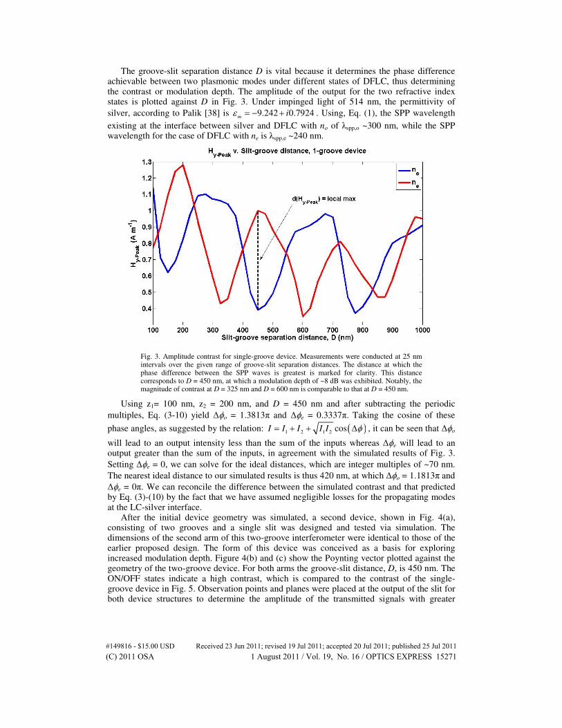
The groove-slit separation distance D is vital because it determines the phase difference achievable between two plasmonic modes under different states of DFLC, thus determining the contrast or modulation depth. The amplitude of the output for the two refractive index states is plotted against D in Fig. 3. Under impinged light of 514 nm, the permittivity of
silver, according to Palik [38] is 9.242 0.7924m
iε = − + . Using, Eq. (1), the SPP wavelength
existing at the interface between silver and DFLC with no of λspp,o ~300 nm, while the SPP wavelength for the case of DFLC with ne is λspp,e ~240 nm.
Fig. 3. Amplitude contrast for single-groove device. Measurements were conducted at 25 nm intervals over the given range of groove-slit separation distances. The distance at which the phase difference between the SPP waves is greatest is marked for clarity. This distance corresponds to D = 450 nm, at which a modulation depth of ~8 dB was exhibited. Notably, the magnitude of contrast at D = 325 nm and D = 600 nm is comparable to that at D = 450 nm.
Using z1= 100 nm, z2 = 200 nm, and D = 450 nm and after subtracting the periodic
multiples, Eq. (3-10) yield ∆φo = 1.3813π and ∆φe = 0.3337π. Taking the cosine of these
phase angles, as suggested by the relation: ( )1 2 1 2cosI I I I I φ= + + ∆ , it can be seen that ∆φo
will lead to an output intensity less than the sum of the inputs whereas ∆φe will lead to an output greater than the sum of the inputs, in agreement with the simulated results of Fig. 3.
Setting ∆φe = 0, we can solve for the ideal distances, which are integer multiples of ~70 nm.
The nearest ideal distance to our simulated results is thus 420 nm, at which ∆φo = 1.1813π and
∆φe = 0π. We can reconcile the difference between the simulated contrast and that predicted by Eq. (3)-(10) by the fact that we have assumed negligible losses for the propagating modes at the LC-silver interface.
After the initial device geometry was simulated, a second device, shown in Fig. 4(a), consisting of two grooves and a single slit was designed and tested via simulation. The dimensions of the second arm of this two-groove interferometer were identical to those of the earlier proposed design. The form of this device was conceived as a basis for exploring increased modulation depth. Figure 4(b) and (c) show the Poynting vector plotted against the geometry of the two-groove device. For both arms the groove-slit distance, D, is 450 nm. The ON/OFF states indicate a high contrast, which is compared to the contrast of the single-groove device in Fig. 5. Observation points and planes were placed at the output of the slit for both device structures to determine the amplitude of the transmitted signals with greater
#149816 - $15.00 USD Received 23 Jun 2011; revised 19 Jul 2011; accepted 20 Jul 2011; published 25 Jul 2011(C) 2011 OSA 1 August 2011 / Vol. 19, No. 16 / OPTICS EXPRESS 15271

detail. As indicated in Fig. 5, by using a double-groove single-slit geometry, a higher ON/OFF contrast could be obtained over the single-groove single-slit geometry.
Fig. 4. (a) Detailed geometry of the double-groove single-slit DFLC-enabled nanoplasmonic modulator. Field intensity plots for the (b) ON state (n = no) and (c) OFF state (n = ne). The relative magnitude of the Poynting vector is shown against the two-dimensional geometry of the device.
#149816 - $15.00 USD Received 23 Jun 2011; revised 19 Jul 2011; accepted 20 Jul 2011; published 25 Jul 2011(C) 2011 OSA 1 August 2011 / Vol. 19, No. 16 / OPTICS EXPRESS 15272

Fig. 5. Intensity contrast for 1-groove and 2-groove devices. The contrast of the 2-groove device is ~15 dB whereas the 1-groove device exhibits contrast of ~8.1 dB.
The contrast, given by Eq. (2), exhibited by our devices is is approximately 8.1 dB and 15 dB for the single-groove and double-groove designs, respectively. Taking into account our
input excitation and pump sources were simulated with 1 A m−1
power densities and the size of the groove and slits, we have a first approximation for the optical part of the switching power of 9.42 pW per operation. The duration of the excitation and pump pulses depends on the type of source. Given that the simulations lasted ~120 fs, the optical energy involved per operation is trivial compared to the electrical part of the switching energy. Based on previous works [21, 32], we gather that the average switching voltage of the DFLCs is 25 V. To calculate electrical switching energy and time, we define an average dielectric function of the
DFLC, ε, as 2 2
22.501
3
o en nε
+= ≈ . The cross-sectional area of our cell is approximated by
assuming a device with a depth equal to the cell length of 450 nm. With these parameters, we compute the cell capacitances for the double-groove device, C ~2.24e-17 F. The capacitance can be used to compute the switching energy, E, by the relation E = CV
2 [8]. Therefore, the
approximate switching energy is E ~14 fJ per operation. Even if the switching voltage is doubled, the switching energy remains in the femotjoule range at ~56 fJ per operation. The switching energy for the single-groove device is simply one half that of the double-groove device.
For the response time τ, we must look into the optical path length of the plasmonic signal, the RC delay imposed by the electrical part of our device, and the rotation time of the DFLC. In the optical limiting case where the device is in the OFF state and n = ne, the transit time of the plasmonic signal is computed with the assumption that the distances between the excitation and the silver-air interface, as well as the slit outlet and a hypothetical detector or adjacent device, are both 1 µm. We find that τtransit = 10.9 fs. For the electrical part of the response time, we impose the assumption that our function generator voltage source has an internal impedance of 50 Ω, and compute τRC = 1.12 fs. Both transit times are much shorter than the limitation imposed by the response time of the LC, which depends on the thickness and applied field strength; for sub-micron thick nematic, the response time is on the order of 100 microseconds [22–24].
The dependence of the contrast on the location of the field monitors was also explored. Figure 6 shows the contrast between the power measured for the two DFLC states for three different observation planes. The planes are located 20 nm, 120 nm, and 220 nm from the bottom slit edge. Using Eq. (2) for all three data sets verifies that the contrast between the SPP propagating through no and ne remains constant regardless of the location of the measurement plane.
#149816 - $15.00 USD Received 23 Jun 2011; revised 19 Jul 2011; accepted 20 Jul 2011; published 25 Jul 2011(C) 2011 OSA 1 August 2011 / Vol. 19, No. 16 / OPTICS EXPRESS 15273

Fig. 6. Intensity contrast for 2-groove device with three different observation planes. The contrast measured at each plane is ~15 dB, verifying that, while the power of the signal decreases with distance from the lower slit edge, the contrast between corresponding no and ne signals remains constant.
To fabricate our proposed devices, focused ion beam can be used to cut the grooves and slits on the silver film with precision control of the width and cutting depth. The processing of DFLC is challenging because we are using a relatively thin film during the simulation. However, with in-plane-designed devices, such as the optical hyperlens [39], impregnation of the liquid crystals is achievable. Future work will consist of fabricating devices in accordance with both the single-groove single-slit and double-groove single-slit geometries. Experiments will be conducted to determine the response time of the liquid crystal switching mechanism for amplitude modulation, the energy required for modulation, and the magnitude of modulation depth.
Conclusion
We have designed and simulated two geometries of DFLC-based, SPP amplitude modulators: (1) single-groove single-slit and (2) double-groove single-slit. Modulation depths greater than 8 dB and 15 dB were exhibited by the single-groove and double-groove devices, respectively. The devices operate at a switching energy on the order of femotjoules; although the plasmonic switching times is on the order of sub-picoseconds, the ultimate response time of the DFLC modulator is limited to 100 microseconds for sub-micron thickness. To our knowledge, this is the first report of a nanoplasmonic modulator employing nanoscale DFLC. With its advantages in modulation depth, energy consumption, and robustness, we anticipate that the proposed nano-structured DFLC-based plasmonic modulators hold promise for many applications where stable and reliable switching of nanophotonic signals is required.
Acknowledgments
We gratefully acknowledge the financial support from Air Force Office of Scientific Research (AFOSR), National Science Foundation (NSF), and the Penn State Center for Nanoscale Science (MRSEC).
#149816 - $15.00 USD Received 23 Jun 2011; revised 19 Jul 2011; accepted 20 Jul 2011; published 25 Jul 2011(C) 2011 OSA 1 August 2011 / Vol. 19, No. 16 / OPTICS EXPRESS 15274