High Common-ModeVoltage Difference · PDF fileCommon-Mode Rejection Ratio (dB) INA149...
26
40 50 60 70 80 90 100 110 120 10 100 1k 10k 100k Frequency (Hz) Common-Mode Rejection Ratio (dB) INA149 Competitor A INA149 www.ti.com SBOS579B – SEPTEMBER 2011 – REVISED JULY 2012 High Common-Mode Voltage Difference Amplifier 1FEATURES DESCRIPTION The INA149 is a precision unity-gain difference 2• Common-Mode Voltage Range: ±275 V amplifier with a very high input common-mode • Minimum CMRR: 90 dB from –40°C to +125°C voltage range. It is a single, monolithic device that • DC Specifications: consists of a precision op amp and an integrated thin- film resistor network. The INA149 can accurately – Maximum Offset Voltage: 1100 μV measure small differential voltages in the presence of – Maximum Offset Voltage Drift: 15 μV/°C common-mode signals up to ±275 V. The INA149 – Maximum Gain Error: 0.02% inputs are protected from momentary common-mode or differential overloads of up to 500 V. – Maximum Gain Error Drift: 10 ppm/°C – Maximum Gain Nonlinearity: 0.001% FSR In many applications, where galvanic isolation in not required, the INA149 can replace isolation amplifiers. • AC Performance: This ability can eliminate costly isolated input side – Bandwidth: 500 kHz power supplies and the associated ripple, noise, and – Typical Slew Rate: 5 V/μs quiescent current. The excellent 0.0005% nonlinearity and 500-kHz bandwidth of the INA149 are superior to • Wide Supply Range: ±2.0 V to ±18 V those of conventional isolation amplifiers. – Maximum Quiescent Current: 900 μA The INA149 is pin-compatible with the INA117 and – Output Swing on ±15-V Supplies: ±13.5 V INA148 type high common-mode voltage amplifiers • Input Protection: and offers improved performance over both devices. – Common-Mode: ±500 V The INA149 is available in the SOIC-8 package with operation specified over the extended industrial – Differential: ±500 V temperature range of –40°C to +125°C. APPLICATIONS • High-Voltage Current Sensing • Battery Cell Voltage Monitoring • Power-Supply Current Monitoring • Motor Controls • Replacement for Isolation Circuits 1 Please be aware that an important notice concerning availability, standard warranty, and use in critical applications of Texas Instruments semiconductor products and disclaimers thereto appears at the end of this data sheet. 2All trademarks are the property of their respective owners. PRODUCTION DATA information is current as of publication date. Copyright © 2011–2012, Texas Instruments Incorporated Products conform to specifications per the terms of the Texas Instruments standard warranty. Production processing does not necessarily include testing of all parameters.
Transcript of High Common-ModeVoltage Difference · PDF fileCommon-Mode Rejection Ratio (dB) INA149...

40
50
60
70
80
90
100
110
120
10 100 1k 10k 100kFrequency (Hz)
Com
mon
−M
ode
Rej
ectio
n R
atio
(dB
) INA149Competitor A
INA149
www.ti.com SBOS579B –SEPTEMBER 2011–REVISED JULY 2012
High Common-Mode Voltage Difference Amplifier1FEATURES DESCRIPTION
The INA149 is a precision unity-gain difference2• Common-Mode Voltage Range: ±275 V
amplifier with a very high input common-mode• Minimum CMRR: 90 dB from –40°C to +125°C voltage range. It is a single, monolithic device that• DC Specifications: consists of a precision op amp and an integrated thin-
film resistor network. The INA149 can accurately– Maximum Offset Voltage: 1100 μVmeasure small differential voltages in the presence of– Maximum Offset Voltage Drift: 15 μV/°C common-mode signals up to ±275 V. The INA149
– Maximum Gain Error: 0.02% inputs are protected from momentary common-modeor differential overloads of up to 500 V.– Maximum Gain Error Drift: 10 ppm/°C
– Maximum Gain Nonlinearity: 0.001% FSR In many applications, where galvanic isolation in notrequired, the INA149 can replace isolation amplifiers.• AC Performance:This ability can eliminate costly isolated input side– Bandwidth: 500 kHz power supplies and the associated ripple, noise, and
– Typical Slew Rate: 5 V/μs quiescent current. The excellent 0.0005% nonlinearityand 500-kHz bandwidth of the INA149 are superior to• Wide Supply Range: ±2.0 V to ±18 Vthose of conventional isolation amplifiers.– Maximum Quiescent Current: 900 μAThe INA149 is pin-compatible with the INA117 and– Output Swing on ±15-V Supplies: ±13.5 VINA148 type high common-mode voltage amplifiers• Input Protection: and offers improved performance over both devices.
– Common-Mode: ±500 V The INA149 is available in the SOIC-8 package withoperation specified over the extended industrial– Differential: ±500 Vtemperature range of –40°C to +125°C.
APPLICATIONS• High-Voltage Current Sensing• Battery Cell Voltage Monitoring• Power-Supply Current Monitoring• Motor Controls• Replacement for Isolation Circuits
1
Please be aware that an important notice concerning availability, standard warranty, and use in critical applications ofTexas Instruments semiconductor products and disclaimers thereto appears at the end of this data sheet.
2All trademarks are the property of their respective owners.
PRODUCTION DATA information is current as of publication date. Copyright © 2011–2012, Texas Instruments IncorporatedProducts conform to specifications per the terms of the TexasInstruments standard warranty. Production processing does notnecessarily include testing of all parameters.

INA149
SBOS579B –SEPTEMBER 2011–REVISED JULY 2012 www.ti.com
This integrated circuit can be damaged by ESD. Texas Instruments recommends that all integrated circuits be handled withappropriate precautions. Failure to observe proper handling and installation procedures can cause damage.
ESD damage can range from subtle performance degradation to complete device failure. Precision integrated circuits may be moresusceptible to damage because very small parametric changes could cause the device not to meet its published specifications.
PACKAGE/ORDERING INFORMATION (1)
PRODUCT PACKAGE-LEAD PACKAGE DESIGNATOR PACKAGE MARKING
INA149 SOIC-8 D INA149A
(1) For the most current package and ordering information, see the Package Option Addendum at the end of this document, or visit thedevice product folder at www.ti.com.
ABSOLUTE MAXIMUM RATINGS (1)
Over operating free-air temperature range, unless otherwise noted.
INA149 UNIT
Supply voltage (V+) – (V–) 40 V
Input voltage range Continuous 300 V
Common-mode and differential, 10 s 500 V
Maximum Voltage on REFA and REFB (V–) – 0.3 to (V+) + 0.3 V
Input current on any input pin (2) 10 mA
Output short-circuit current duration Indefinite
Operating temperature range –55 to +150 °C
Storage temperature range –65 to +150 °C
Junction temperature +150 °C
Human body model (HBM) 1500 V
ESD rating Charged device model (CDM) 1000 V
Machine model (MM) 100 V
(1) Stresses above these ratings may cause permanent damage. Exposure to absolute maximum conditions for extended periods maydegrade device reliability. These are stress ratings only, and functional operation of the device at these or any other conditions beyondthose specified is not implied.
(2) REFA and REFB are diode clamped to the power-supply rails. Signals applied to these pins that can swing more than 0.3 V beyond thesupply rails should be limited to 10 mA or less.
2 Submit Documentation Feedback Copyright © 2011–2012, Texas Instruments Incorporated
Product Folder Link(s): INA149

INA149
www.ti.com SBOS579B –SEPTEMBER 2011–REVISED JULY 2012
ELECTRICAL CHARACTERISTICS: V+ = +15 V and V– = –15 VAt TA = +25°C, RL = 2 kΩ connected to ground, and VCM = REFA = REFB = GND, unless otherwise noted.
INA149
PARAMETER TEST CONDITIONS MIN TYP MAX UNIT
GAIN
Initial VOUT = ±10.0 V 1 V/V
Gain error VOUT = ±10.0 V ±0.005 ±0.02 %FSR
Gain vs temperature, TA = –40°C to +125°C ±1.5 ±10 ppm/°C
Nonlinearity ±0.0005 ±0.001 %FSR
OFFSET VOLTAGE
350 1100 µV
Initial offset vs temperature, TA = –40°C to +125°C 3 15 µV/°C
vs supply (PSRR), VS = ±2 V to ±18 V 90 120 dB
INPUT
Differential 800 kΩImpedance
Common-mode 200 kΩDifferential –13.5 13.5 V
Voltage rangeCommon-mode –275 275 V
At dc, VCM = ±275 V 90 100 dB
vs temperature, TA = –40°C to +125°C, at dc 90 dBCommon-mode rejection(CMRR) At ac, 500 Hz, VCM = 500 VPP 90 dB
At ac, 1 kHz, VCM = 500 VPP 90 dB
OUTPUT
Voltage range –13.5 13.5 V
Short-circuit current ±25 mA
Capacitive load drive No sustained oscillations 10 nF
OUTPUT NOISE VOLTAGE
0.01 Hz to 10 Hz 20 µVPP
10 kHz 550 nV/√Hz
DYNAMIC RESPONSE
Small-signal bandwidth 500 kHz
Slew rate VOUT = ±10-V step 1.7 5 V/µs
Full-power bandwidth VOUT = 20 VPP 32 kHz
Settling time 0.01%, VOUT = 10-V step 7 µs
POWER SUPPLY
Voltage range ±2 ±18 V
VS = ±18 V, VOUT = 0 V 810 900 µAQuiescent current
vs temperature, TA = –40°C to +125°C 1.1 mA
TEMPERATURE RANGE
Specified –40 +125 °C
Operating –55 +150 °C
Storage –65 +150 °C
Copyright © 2011–2012, Texas Instruments Incorporated Submit Documentation Feedback 3
Product Folder Link(s): INA149

INA149
SBOS579B –SEPTEMBER 2011–REVISED JULY 2012 www.ti.com
ELECTRICAL CHARACTERISTICS: V+ = 5 V and V– = 0 VAt TA = +25°C, RL = 2 kΩ connected to 2.5 V, and VCM= REFA = REFB = 2.5 V, unless otherwise noted.
INA149
PARAMETER TEST CONDITIONS MIN TYP MAX UNIT
GAIN
Initial VOUT = 1.5 V to 3.5 V 1 V/V
Gain error VOUT = 1.5 V to 3.5 V ±0.005 %FSR
Gain vs temperature, TA = –40°C to +125°C ±1.5 ppm/°C
Nonlinearity ±0.0005 %FSR
OFFSET VOLTAGE
350 µV
Initial offset vs temperature, TA = –40°C to +125°C 3 µV/°C
vs supply (PSRR), VS = 4 V to 5 V 120 dB
INPUT
Differential 800 kΩImpedance
Common-mode 200 kΩDifferential 1.5 3.5 V
Voltage rangeCommon-mode –20 25 V
At dc, VCM = –20 V to 25 V 100 dB
vs temperature, TA = –40°C to +125°C, at dc 100 dBCommon-mode rejection
At ac, 500 Hz, VCM = 49 VPP 100 dB
At ac, 1 kHz, VCM = 49 VPP 90 dB
OUTPUT
Voltage range 1.5 3.5 V
Short-circuit current ±15 mA
Capacitive load drive No sustained oscillations 10 nF
OUTPUT NOISE VOLTAGE
0.01 Hz to 10 Hz 20 µVPP
10 kHz 550 nV/√Hz
DYNAMIC RESPONSE
Small-signal bandwidth 500 kHz
Slew rate VOUT = 2 VPP step 5 V/µs
Full-power bandwidth VOUT = 2 VPP 32 kHz
Settling time 0.01%, VOUT = 2 VPP step 7 µs
POWER SUPPLY
Voltage range 5 V
VS = 5 V 810 µAQuiescent current
vs temperature, TA = –40°C to +125°C 1 mA
4 Submit Documentation Feedback Copyright © 2011–2012, Texas Instruments Incorporated
Product Folder Link(s): INA149

6
8
3
1
2 7
4 5
NC
V+
VOUT
REFB
−IN
+IN
+
20 kΩ 380 kΩ
380 kΩ
380 kΩ
19 kΩ
REFAV−
INA149
www.ti.com SBOS579B –SEPTEMBER 2011–REVISED JULY 2012
THERMAL INFORMATIONINA149
THERMAL METRIC (1) D (SOIC) UNITS
8 PINS
θJA Junction-to-ambient thermal resistance 110
θJCtop Junction-to-case (top) thermal resistance 57
θJB Junction-to-board thermal resistance 54°C/W
ψJT Junction-to-top characterization parameter 11
ψJB Junction-to-board characterization parameter 53
θJCbot Junction-to-case (bottom) thermal resistance N/A
(1) For more information about traditional and new thermal metrics, see the IC Package Thermal Metrics application report, SPRA953.PIN CONFIGURATION
D PACKAGESOIC-8
(TOP VIEW)
PIN DESCRIPTIONSNAME NO. DESCRIPTION
–IN 2 Inverting input
+IN 3 Noninverting input
NC 8 No internal connection
REFA 5 Reference input
REFB 1 Reference input
V– 4 Negative power supply
V+ 7 Positive power supply (1)
VOUT 6 Output
(1) In this document, (V+) – (V–) is referred to as VS.
Copyright © 2011–2012, Texas Instruments Incorporated Submit Documentation Feedback 5
Product Folder Link(s): INA149

−20 −16 −12 −8 −4 0 4 8 12 16 20Output Voltage (V)
Out
put E
rror
(2
mV
/div
)
VS = ±18 VVS = ±15 V
VS = ±12 VVS = ±10 V
G004
−20 −16 −12 −8 −4 0 4 8 12 16 20Output Voltage (V)
Out
put E
rror
(2
mV
/div
)
VS = ±18 VVS = ±15 V
VS = ±12 VVS = ±10 V
G005
0
50
100
150
200
250
300
350
400
0 2 4 6 8 10 12 14 16 18 20Power−Supply Voltage (±V)
Com
mon
−M
ode
Ope
ratin
g R
ange
(±V
)
G002
−20 −16 −12 −8 −4 0 4 8 12 16 20Output Voltage (V)
Out
put E
rror
(2
mV
/div
)
VS = ±18 VVS = ±15 V
VS = ±12 VVS = ±10 V
G003
0
20
40
60
80
100
120
10 100 1k 10k 100k 1M 10MFrequency (Hz)
Com
mon
−M
ode
Rej
ectio
n R
atio
(dB
) −40°C+25°C+125°C
G001
−6
−4
−2
0
2
4
6
−400 −300 −200 −100 0 100 200 300 400Common−Mode Input Voltage (V)
Out
put V
olta
ge (
mV
)
VS = ±18 VVS = ±15 VVS = ±10 VVS = ±5 V
G066
INA149
SBOS579B –SEPTEMBER 2011–REVISED JULY 2012 www.ti.com
TYPICAL CHARACTERISTICSAt TA = +25°C, RL = 2 kΩ connected to ground, and VS = ±15 V, unless otherwise noted.
CMRR vs FREQUENCY COMMON-MODE REJECTION
Figure 1. Figure 2.
COMMON-MODE OPERATING RANGE TYPICAL GAIN ERROR FOR RL = 10 kΩvs POWER-SUPPLY VOLTAGE (Curves Offset for Clarity)
Figure 3. Figure 4.
TYPICAL GAIN ERROR FOR RL = 2 kΩ TYPICAL GAIN ERROR FOR RL = 1 kΩ(Curves Offset for Clarity) (Curves Offset for Clarity)
Figure 5. Figure 6.
6 Submit Documentation Feedback Copyright © 2011–2012, Texas Instruments Incorporated
Product Folder Link(s): INA149

−10
−8
−6
−4
−2
0
2
4
6
8
10
−12 −10 −8 −6 −4 −2 0 2 4 6 8 10 12Output Voltage (V)
Err
or (
ppm
)
VS = ±12 VRL = 10 kΩ
G062
−20
−15
−10
−5
0
5
10
15
20
0 5 10 15 20 25 30 35Output Current (mA)
Out
put V
olta
ge (
V)
−45°C+25°C+85°C+130°C
G017
−10
−8
−6
−4
−2
0
2
4
6
8
10
−12 −10 −8 −6 −4 −2 0 2 4 6 8 10 12Output Voltage (V)
Err
or (
ppm
)
VS = ±15 VRL = 2 kΩ
G015
−10
−8
−6
−4
−2
0
2
4
6
8
10
−12 −10 −8 −6 −4 −2 0 2 4 6 8 10 12Output Voltage (V)
Err
or (
ppm
)
VS = ±15 VRL = 1 kΩ
G016
−5 −4 −3 −2 −1 0 1 2 3 4 5Output Voltage (V)
Out
put E
rror
(2
mV
/div
)
VS = ±5 VVS = ±5 V
VS = ±5 VVS = ±2.5 V
RL = 10 kΩ
RL = 2 kΩ
RL = 1 kΩ
RL = 1 kΩ
G006
−10
−8
−6
−4
−2
0
2
4
6
8
10
−12 −10 −8 −6 −4 −2 0 2 4 6 8 10 12Output Voltage (V)
Err
or (
ppm
)
VS = ±15 VRL = 10 kΩ
G014
INA149
www.ti.com SBOS579B –SEPTEMBER 2011–REVISED JULY 2012
TYPICAL CHARACTERISTICS (continued)At TA = +25°C, RL = 2 kΩ connected to ground, and VS = ±15 V, unless otherwise noted.
TYPICAL GAIN ERROR FOR LOW SUPPLY VOLTAGES(Curves Offset for Clarity) GAIN NONLINEARITY
Figure 7. Figure 8.
GAIN NONLINEARITY GAIN NONLINEARITY
Figure 9. Figure 10.
GAIN NONLINEARITY OUTPUT VOLTAGE vs LOAD CURRENT
Figure 11. Figure 12.
Copyright © 2011–2012, Texas Instruments Incorporated Submit Documentation Feedback 7
Product Folder Link(s): INA149

0
10
20
30
40
50
60
70
80
90
100
110
120
10 100 1k 10k 100kFrequency (Hz)
Pow
er−
Sup
ply
Rej
ectio
n R
atio
(dB
) −40°C+25°C+125°C
G064
0
0.2
0.4
0.6
0.8
1
1.2
1.4
1.6
1.8
2
−60 −40 −20 0 20 40 60 80 100 120 140 160Ambient Temperature (°C)
Max
imum
Pow
er D
issi
patio
n (W
)
G013
−50−50
Time (10 s/div)
Noi
se (
10 µ
V/d
iv)
G070
0
10
20
30
40
50
60
70
80
90
100
110
120
10 100 1k 10k 100kFrequency (Hz)
Pow
er−
Sup
ply
Rej
ectio
n R
atio
(dB
) −40°C+25°C+125°C
G009
−80
−60
−40
−20
0
20
100 1k 10k 100k 1M 10MFrequency (Hz)
Gai
n (d
B)
25 °C−40 °C125 °C
G010
400
500
600
700
800
900
1000
1 10 100 1k 10k 100kFrequency (Hz)
Noi
se S
pect
ral D
ensi
ty (
nV/
Hz
)
G008
INA149
SBOS579B –SEPTEMBER 2011–REVISED JULY 2012 www.ti.com
TYPICAL CHARACTERISTICS (continued)At TA = +25°C, RL = 2 kΩ connected to ground, and VS = ±15 V, unless otherwise noted.
GAIN vs FREQUENCY NOISE SPECTRAL DENSITY vs FREQUENCY
Figure 13. Figure 14.
0.01 Hz TO 10 Hz NOISE POSITIVE PSRR vs FREQUENCY
Figure 15. Figure 16.
NEGATIVE PSRR vs FREQUENCY MAXIMUM POWER DISSIPATION vs TEMPERATURE
Figure 17. Figure 18.
8 Submit Documentation Feedback Copyright © 2011–2012, Texas Instruments Incorporated
Product Folder Link(s): INA149

−30
−27
−24
−21
−18
−15
−12 −
9−
6−
3 0 3 6 9 12 15 18 21 24 27 30
−30
−27
−24
−21
−18
−15
−12 −
9−
6−
3 0 3 6 9 12 15 18 21 24 27 30
0
2
4
6
8
10
12
14
16
18
20
CMRR (µV/V)
Per
cent
of P
opul
atio
n (~
5 kU
)
G019
−1.4
−1.2
−1
−0.8
−0.6
−0.4
−0.2
0
0.2
−4
−2
0
2
4
6
8
10
12
Time (5 us/div)
Err
or V
olta
ge (
mV
)
Out
put V
olta
ge (
V)
Error VoltageOutput Voltage
G063
−100
−80
−60
−40
−20
0
20
40
60
80
100
120
140
0 20 40 60 80 100 120Time (µs)
Vol
tage
(m
V)
0 nF1 nF3 nF5 nF10 nF
G065
−0.2
0
0.2
0.4
0.6
0.8
1
1.2
1.4
−12
−10
−8
−6
−4
−2
0
2
4
Time (5 us/div)
Err
or V
olta
ge (
mV
)
Out
put V
olta
ge (
V)
Error VoltageOutput Voltage
G018
Time (4 µs/div)
Out
put V
olta
ge (
5 V
/div
)
CL = 1000 pFRL = 2 kΩ
G011
Time (4 µs/div)
Out
put V
olta
ge (
25 m
V/d
iv)
CL = 1000 pFRL = 2 kΩ
G012
INA149
www.ti.com SBOS579B –SEPTEMBER 2011–REVISED JULY 2012
TYPICAL CHARACTERISTICS (continued)At TA = +25°C, RL = 2 kΩ connected to ground, and VS = ±15 V, unless otherwise noted.
LARGE-SIGNAL STEP RESPONSE SMALL-SIGNAL STEP RESPONSE
Figure 19. Figure 20.
SMALL-SIGNAL RESPONSE vs CAPACITIVE LOAD SETTLING TIME
Figure 21. Figure 22.
SETTLING TIME CMRR HISTOGRAM
Figure 23. Figure 24.
Copyright © 2011–2012, Texas Instruments Incorporated Submit Documentation Feedback 9
Product Folder Link(s): INA149
−2000
−1600
−1200
−800
−400
0
400
800
1200
1600
2000
−75 −50 −25 0 25 50 75 100 125 150 175Temperature (°C)
Offs
et V
olta
ge (µ
V)
G027
−50
−40
−30
−20
−10
0
10
20
30
40
50
−75 −50 −25 0 25 50 75 100 125 150 175Temperature (°C)
CM
RR
(µV
/V)
G028
−1.
50−
1.35
−1.
20−
1.05
−0.
90−
0.75
−0.
60−
0.45
−0.
30−
0.15
0.00
0.15
0.30
0.45
0.60
0.75
0.90
1.05
1.20
1.35
1.50
−1.
50−
1.35
−1.
20−
1.05
−0.
90−
0.75
−0.
60−
0.45
−0.
30−
0.15
0.00
0.15
0.30
0.45
0.60
0.75
0.90
1.05
1.20
1.35
1.50
0
5
10
15
20
25
30
35
PSRR (µV/V)
Per
cent
of P
opul
atio
n (~
5 kU
)
G025
0.10
0.11
0.12
0.13
0.14
0.15
0.16
0.17
0.18
0.19
0.20
0.21
0.22
0.23
0.24
0.25
0.26
0.27
0.28
0.29
0.30
0.10
0.11
0.12
0.13
0.14
0.15
0.16
0.17
0.18
0.19
0.20
0.21
0.22
0.23
0.24
0.25
0.26
0.27
0.28
0.29
0.30
0
5
10
15
20
25
30
35
Nonlinearity Error (m%)
Per
cent
of P
opul
atio
n (~
5 kU
)
G026
−10
00−
900
−80
0−
700
−60
0−
500
−40
0−
300
−20
0−
100 0
100
200
300
400
500
600
700
800
900
1000
−10
00−
900
−80
0−
700
−60
0−
500
−40
0−
300
−20
0−
100 0
100
200
300
400
500
600
700
800
900
1000
0
2
4
6
8
10
12
Offset Voltage (µV)
Per
cent
of P
opul
atio
n (~
5 kU
)
G022
−20
−18
−16
−14
−12
−10 −
8−
6−
4−
2 0 2 4 6 8 10 12 14 16 18 20
−20
−18
−16
−14
−12
−10 −
8−
6−
4−
2 0 2 4 6 8 10 12 14 16 18 20
0
2
4
6
8
10
12
14
16
18
20
Differential Gain Error (m%)
Per
cent
of P
opul
atio
n (~
5 kU
)
G024
INA149
SBOS579B –SEPTEMBER 2011–REVISED JULY 2012 www.ti.com
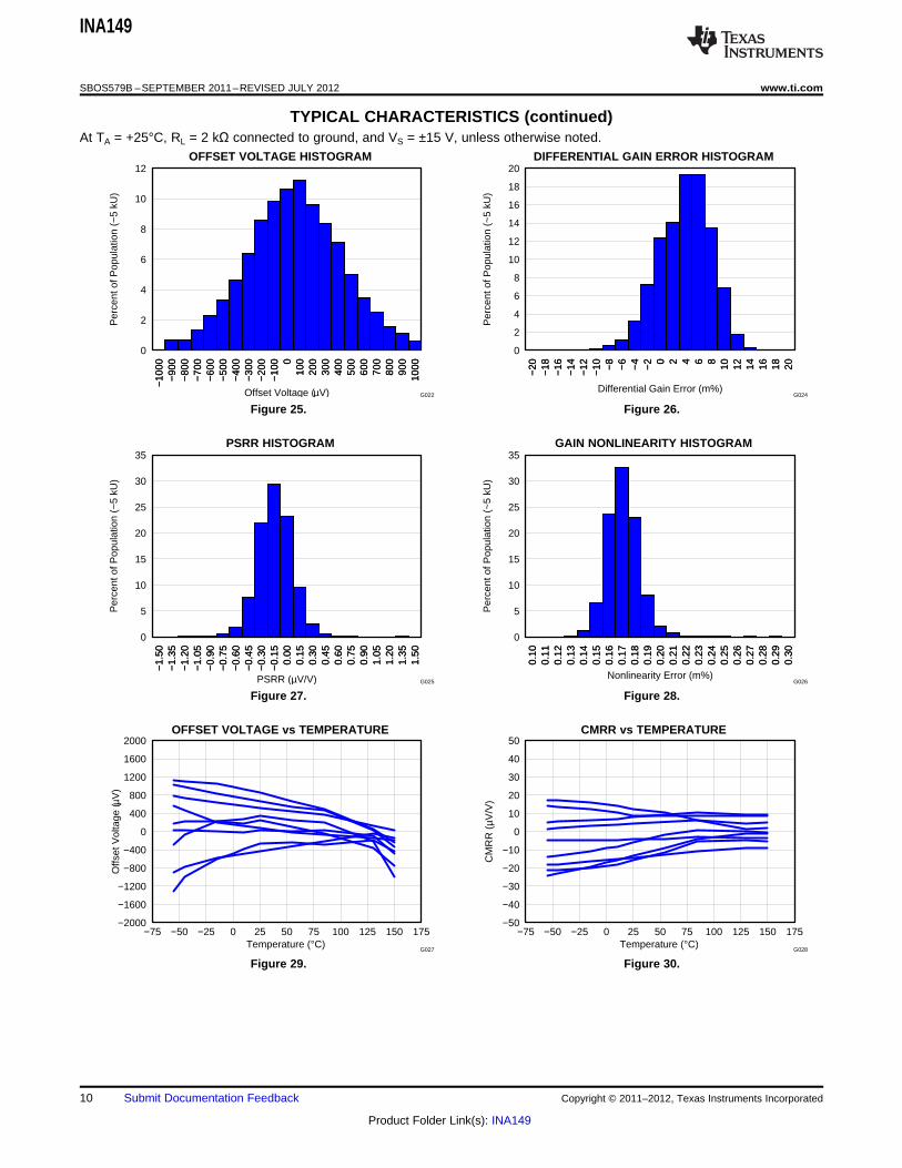
TYPICAL CHARACTERISTICS (continued)At TA = +25°C, RL = 2 kΩ connected to ground, and VS = ±15 V, unless otherwise noted.
OFFSET VOLTAGE HISTOGRAM DIFFERENTIAL GAIN ERROR HISTOGRAM
Figure 25. Figure 26.
PSRR HISTOGRAM GAIN NONLINEARITY HISTOGRAM
Figure 27. Figure 28.
OFFSET VOLTAGE vs TEMPERATURE CMRR vs TEMPERATURE
Figure 29. Figure 30.
10 Submit Documentation Feedback Copyright © 2011–2012, Texas Instruments Incorporated
Product Folder Link(s): INA149

0
1
2
3
4
5
0 5 10 15 20 25 30 35 40Supply Voltage (V)
Sle
w R
ate
(V/µ
s)
Negative Slew RatePositive Slew Rate
G038
400
600
800
1000
1200
−75 −50 −25 0 25 50 75 100 125 150 175Temperature (°C)
Cur
rent
(µA
)
G043
−5
−4
−3
−2
−1
0
1
2
3
4
5
−75 −50 −25 0 25 50 75 100 125 150 175Temperature (°C)
Line
arity
Err
or (
m%
)
G031
2
3
4
5
6
7
8
−75 −25 25 75 125 175Temperature (°C)
Sle
w R
ate
(V/µ
s)
G071
−2
−1.6
−1.2
−0.8
−0.4
0
0.4
0.8
1.2
1.6
2
−75 −50 −25 0 25 50 75 100 125 150 175Temperature (°C)
PS
RR
(µV
/V)
G029
−50
−40
−30
−20
−10
0
10
20
30
40
50
−75 −50 −25 0 25 50 75 100 125 150 175Temperature (°C)
Gai
n E
rror
(m
%)
G030
INA149
www.ti.com SBOS579B –SEPTEMBER 2011–REVISED JULY 2012
TYPICAL CHARACTERISTICS (continued)At TA = +25°C, RL = 2 kΩ connected to ground, and VS = ±15 V, unless otherwise noted.
PSRR vs TEMPERATURE GAIN ERROR vs TEMPERATURE
Figure 31. Figure 32.
GAIN NONLINEARITY vs TEMPERATURE SLEW RATE vs TEMPERATURE
Figure 33. Figure 34.
SLEW RATE vs POWER-SUPPLY VOLTAGE QUIESCENT CURRENT vs TEMPERAUTRE
Figure 35. Figure 36.
Copyright © 2011–2012, Texas Instruments Incorporated Submit Documentation Feedback 11
Product Folder Link(s): INA149

0.70
0.71
0.72
0.73
0.74
0.75
0.76
0.77
0.78
0.79
0.80
0.81
0.82
0.83
0.84
0.85
0.86
0.87
0.88
0.89
0.90
0.70
0.71
0.72
0.73
0.74
0.75
0.76
0.77
0.78
0.79
0.80
0.81
0.82
0.83
0.84
0.85
0.86
0.87
0.88
0.89
0.90
0
5
10
15
20
25
30
35
40
45
50
Quiescent Current (mA)
Per
cent
of P
opul
atio
n (~
5 kU
)
G059
−16
−12
−8
−4
0
4
Time (1 µs/div)
Vol
tage
(V
)
InputOutput
G067
0
5
10
15
20
25
30
1k 10k 100k 1MFrequency (Hz)
Max
imum
Out
put V
olta
ge (
±V)
G057
−4
0
4
8
12
16
Time (1 µs/div)
Vol
tage
(V
)
InputOutput
G058
−90
−80
−70
−60
−50
−40
−30
−20
−10
0
10
100 1k 10k 100k 1M 10MFrequency (Hz)
VO
UT /
VIN
(dB
)
0 nF1 nF3 nF5 nF10 nF
G044
0
200
400
600
800
1000
1200
0 2 4 6 8 10 12 14 16 18 20Supply Voltage (±V)
Qui
esce
nt C
urre
nt (
µA)
−45°C +25°C +85°C +130°C
G056
INA149
SBOS579B –SEPTEMBER 2011–REVISED JULY 2012 www.ti.com
TYPICAL CHARACTERISTICS (continued)At TA = +25°C, RL = 2 kΩ connected to ground, and VS = ±15 V, unless otherwise noted.
FREQUENCY RESPONSE vs CAPACITIVE LOAD QUIESCENT CURRENT vs SUPPLY VOLTAGE
Figure 37. Figure 38.
MAXIMUM OUTPUT VOLTAGE vs FREQUENCY OVERLOAD RECOVERY
Figure 39. Figure 40.
OVERLOAD RECOVERY QUIESCENT CURRENT HISTOGRAM
Figure 41. Figure 42.
12 Submit Documentation Feedback Copyright © 2011–2012, Texas Instruments Incorporated
Product Folder Link(s): INA149

+
20 kΩ 380 kΩ
380 kΩ
380 kΩ
19 kΩ
30 V
1 F
GND
4 7
2
3
1
6
5
−IN
+IN VOUT = (+IN) – (–IN) + VREF
VREF
100 nF
+
20 kΩ 380 kΩ
380 kΩ
380 kΩ
19 kΩ
−15 V
1 F
15 V
1 F
GND
4 7
2
3
1
6
5
−IN
+IN VOUT = (+IN) − (−IN)
100 nF100 nF
INA149
www.ti.com SBOS579B –SEPTEMBER 2011–REVISED JULY 2012
APPLICATION INFORMATION
BASIC INFORMATION
Figure 43 shows the basic connections required for dual-supply operation. Applications with noisy or high-impedance power-supply lines may require decoupling capacitors placed close to the device pins. The outputvoltage is equal to the differential input voltage between pins 2 and 3. The common-mode input voltage isrejected. Figure 44 shows the basic connections required for single-supply operation.
Figure 43. Basic Power and Signal Connections for Figure 44. Basic Power and Signal Connections forDual-Supply Operation Single-Supply Operation
TRANSFER FUNCTION
Most applications use the INA149 as a simple unity-gain difference amplifier. The transfer function is given inEquation 1:VOUT = (+IN) – (–IN) (1)
Some applications, however, apply voltages to the reference terminals (REFA and REFB). The complete transferfunction is given in Equation 2:VOUT = (+IN) – (–IN) + 20 × REFA – 19 × REFB (2)
COMMON-MODE RANGE
The high common-mode range of the INA149 is achieved by dividing down the input signal with a high precisionresistor divider. This resistor divider brings both the positive input and the negative input within the input range ofthe internal operational amplifier. This input range depends on the supply voltage of the INA149.
Both Figure 2 and Figure 3 can be used to determine the maximum common-mode range for a specific supplyvoltage. The maximum common-mode range can also be calculated by ensuring that both the positive and thenegative input of the internal amplifier are within 1.5 V of the supply voltage.
In case the voltage at the inputs of the internal amplifier exceeds the supply voltage, the internal ESD diodesstart conducting current. This current must be limited to 10 mA to make sure not to exceed the absolutemaximum ratings for the device.
Copyright © 2011–2012, Texas Instruments Incorporated Submit Documentation Feedback 13
Product Folder Link(s): INA149

+
20 kΩ 380 kΩ
380 kΩ
380 kΩ
19 kΩ
−15 V
15 V
4 7
2
3
1
6
5
−IN
+IN VOUT = (+IN) − (−IN)
+
15 V
−15 V
100 Ω
100 Ω
100 µA
½ REF200
100 µA
½ REF200
10 kΩ
(1)
INA149
SBOS579B –SEPTEMBER 2011–REVISED JULY 2012 www.ti.com
COMMON-MODE REJECTION
Common-mode rejection (CMR) of the INA149 depends on the input resistor network, which is laser-trimmed foraccurate ratio matching. To maintain high CMR, it is important to have low source impedance driving the twoinputs. A 75-Ω resistance in series with pins 2 or 3 decreases the common-mode rejection ratio (CMRR) from100 dB (typical) to 74 dB.
Resistance in series with the reference pins also degrades CMR. A 4-Ω resistance in series with pins 1 or 5decreases CMRR from 100 dB to 74 dB.
Most applications do not require trimming. Figure 45 shows an optional circuit that may be used for trimmingoffset voltage and common-mode rejection.
(1) The OPA171 (a 36-V, low-power, RRO, general-purpose operational amplifier) can be used for this application.
Figure 45. Offset Voltage Trim Circuit
14 Submit Documentation Feedback Copyright © 2011–2012, Texas Instruments Incorporated
Product Folder Link(s): INA149

+
20 kΩ 380 kΩ
380 kΩ
380 kΩ
19 kΩ
V− V+
4 7
2
3
1
6
5
VO = RS × IDUT+
RS
Device
Under
Test
IDUT+
(+275 V max)
+VS
+
20 kΩ 380 kΩ
380 kΩ
380 kΩ
19 kΩ
V− V+
4 7
2
3
1
6
5
RS
RC(1)
IDUT−
−VS
(−275 V max)
VO = RS × IDUT−
RC(1)
INA149
www.ti.com SBOS579B –SEPTEMBER 2011–REVISED JULY 2012
MEASURING CURRENT
The INA149 can be used to measure a current by sensing the voltage drop across a series resistor, RS.Figure 46 shows the INA149 used to measure the supply currents of a device under test.
The sense resistor imbalances the input resistor matching of the INA149, thus degrading its CMR. Also, the inputimpedance of the INA149 loads RS, causing gain error in the voltage-to-current conversion. Both of these errorscan be easily corrected.
The CMR error can be corrected with the addition of a compensation resistor (RC), equal to the value of RS, asshown in Figure 46. If RS is less than 5 Ω, degradation in the CMR is negligible and RC can be omitted. If RS islarger than approximately 1 kΩ, trimming RC may be required to achive greater than 90-dB CMR. This error iscaused by the INA149 input impedance mismatch.
Figure 46. Measuring Supply Currents of a Device Under Test
If RS is more than approximately 50 Ω, the gain error is greater than the 0.02% specification of the INA149. Thisgain error can be corrected by slightly increasing the value of RS. The corrected value (RS') can be calculated byRS' = RS × 380 kΩ/(380 kΩ – RS) (3)
Example: For a 1-V/mA transfer function, the nominal, uncorrected value for RS would be 1 kΩ. A slightly largervalue (RS' = 1002.6 Ω), compensates for the gain error as a result of loading.
The 380-kΩ term in the equation for RS' has a tolerance of 25%, thus sense resistors above approximately 400 Ωmay require trimming to achive gain accuracy better than 0.02%.
Copyright © 2011–2012, Texas Instruments Incorporated Submit Documentation Feedback 15
Product Folder Link(s): INA149

+
20 kΩ 380 kΩ
380 kΩ
380 kΩ
19 kΩ
V− V+
4 7
2
3
1
6
5
+VOUT = (+IN) – (–IN)
–IN
+IN
R1 R2
C2
C1
(1)
INA149
SBOS579B –SEPTEMBER 2011–REVISED JULY 2012 www.ti.com
NOISE PERFORMANCE
The wideband noise performane of the INA149 is dominated by the internal resistor network. The thermal orJohnson noise of these resistors measures approximately 550 nV/√Hz. The internal op amp contributes virtuallyno excess noise at frequencies above 100 Hz.
Many applications may be satisfied with less than the full 500-kHz bandwidth of the INA149. In these cases, thenoise can be reduced with a low-pass filter on the output. The two-pole filter shown in Figure 47 limits bandwidthand reduces noise. Because the INA149 has a 1/f noise corner frequency of approximately 100 Hz, a cutofffrequency below 100 Hz does not further reduce noise.
Component values for different filter frequencies are shown in Table 1.
(1) For most applications, the OPA171 can be used as an operational amplifier. For directly driving successive-approximation register (SAR)data converters, the OPA140 is a good choice.
Figure 47. Output Filter for Noise Reduction
Table 1. Components Values for Different Filter Bandwidths
BUTTERWORTH OUTPUT NOISELOW-PASS (f–3 dB) (mVPP) R1 R2 C1 C2
200 kHz 1.8 No filter
100 kHz 1.1 11 kΩ 11.3 kΩ 100 pF 200 pF
10 kHz 0.35 11 kΩ 11.3 kΩ 1 nF 2 nF
1 kHz 0.11 11 kΩ 11.3 kΩ 10 nF 20 nF
100 Hz 0.05 11 kΩ 11.3 kΩ 0.1 µF 0.2 µF
16 Submit Documentation Feedback Copyright © 2011–2012, Texas Instruments Incorporated
Product Folder Link(s): INA149

+
20 kΩ 380 kΩ
380 kΩ
380 kΩ
19 kΩ
V− = −15 V V+ = +15 V
4 7
2
3
1
6
5
VOUT
RS = 10 Ω
VCM = 265 V
RC = 10 Ω(1)
IMAX = 1 A
INA149
www.ti.com SBOS579B –SEPTEMBER 2011–REVISED JULY 2012
ERROR BUDGET ANALYSIS
The following error budget analysis demonstrates the importance of a high common-mode rejection ratio whenmeasuring small differential signals in the presence of high common-mode voltages. Figure 48 shows a typicalcurrent measurement application.
(1) See the Measuring Current section for details about RC.
Figure 48. Typical Current Measurement Application
The maximum current through the shunt resistor (RS) is 1 A and generates a full-scale voltage drop of 10 V. Allerror sources in this calculation are shown in relation to this full-scale voltage. The common-mode voltage in thisscenario is 265 V and the temperature range is from room temperature (+25°C) to +85°C. Table 2 shows thedominant error sources for the INA149 and a competitor device.
Table 2. Error Budget Analysis
ERROR (ppm of FS)ERRORSOURCE INA149 COMPETIOR A INA149 COMPETITOR A
Accuracy, TA = +25°C
Initial gain error 0.02% FS 0.05% FS 200 500
Offset voltage 1100 µV 1000 µV 110 100
Common mode 265 V/90 dB = 8380 µV 265 V/77 dB = 37432 µV 838 3743
Total acuracy error 1148 4343
Temperature drift
Gain 10 ppm/°C × 60°C 10 ppm/°C × 60°C 600 600
Offset voltage 10 µV/°C × 60°C 20 µV/°C × 60°C 60 120
Total drift error 660 720
Total error 1808 5063
If a smaller shunt resistor is used, the full-scale voltage drop is also smaller. A shunt resistor of 1 Ω causes a 1-Vvoltage drop with a current of 1 A flowing through it. The error of 1808 ppm for a full-scale voltage of 10 Vbecomes 18080 ppm (1.6%) for a full-scale voltage of only 1 V.
This example demonstrates that the dominate source of error, even over temperature, comes from the CMRRspecification of the devices. The common-mode error is 46% of the total error for the INA149 and 74% of thetotal error for the competitor device.
Copyright © 2011–2012, Texas Instruments Incorporated Submit Documentation Feedback 17
Product Folder Link(s): INA149

2
3
(+275 V max)
+VS
−VS
(−275 V max)
+
INA149
2
3+
INA149
2
3+
INA149
2
3+
INA149
Repeat
for each
cell
ADS8638
12-bit, 8-Channel,
Bipolar SAR ADC
MSP430
16-Bit Ultra-Low-
Power Microcontroller
INA149
SBOS579B –SEPTEMBER 2011–REVISED JULY 2012 www.ti.com
BATTERY CELL VOLTAGE MONITOR
The INA149 can be used to measure the voltages of single cells in a stacked battery pack. Figure 49 shows anexamples for such an application.
Figure 49. Battery Cell Voltage Monitor
18 Submit Documentation Feedback Copyright © 2011–2012, Texas Instruments Incorporated
Product Folder Link(s): INA149

INA149
www.ti.com SBOS579B –SEPTEMBER 2011–REVISED JULY 2012
REVISION HISTORY
NOTE: Page numbers for previous revisions may differ from page numbers in the current version.
Changes from Revision A (November 2011) to Revision B Page
• Changed package marking data in Package/Ordering Information table ............................................................................. 2
Copyright © 2011–2012, Texas Instruments Incorporated Submit Documentation Feedback 19
Product Folder Link(s): INA149

PACKAGE OPTION ADDENDUM
www.ti.com 10-Jul-2012
Addendum-Page 1
PACKAGING INFORMATION
Orderable Device Status (1) Package Type PackageDrawing
Pins Package Qty Eco Plan (2) Lead/Ball Finish
MSL Peak Temp (3) Samples
(Requires Login)
INA149AID ACTIVE SOIC D 8 75 Green (RoHS& no Sb/Br)
CU NIPDAU Level-2-260C-1 YEAR
INA149AIDR ACTIVE SOIC D 8 2500 Green (RoHS& no Sb/Br)
CU NIPDAU Level-2-260C-1 YEAR
(1) The marketing status values are defined as follows:ACTIVE: Product device recommended for new designs.LIFEBUY: TI has announced that the device will be discontinued, and a lifetime-buy period is in effect.NRND: Not recommended for new designs. Device is in production to support existing customers, but TI does not recommend using this part in a new design.PREVIEW: Device has been announced but is not in production. Samples may or may not be available.OBSOLETE: TI has discontinued the production of the device.
(2) Eco Plan - The planned eco-friendly classification: Pb-Free (RoHS), Pb-Free (RoHS Exempt), or Green (RoHS & no Sb/Br) - please check http://www.ti.com/productcontent for the latest availabilityinformation and additional product content details.TBD: The Pb-Free/Green conversion plan has not been defined.Pb-Free (RoHS): TI's terms "Lead-Free" or "Pb-Free" mean semiconductor products that are compatible with the current RoHS requirements for all 6 substances, including the requirement thatlead not exceed 0.1% by weight in homogeneous materials. Where designed to be soldered at high temperatures, TI Pb-Free products are suitable for use in specified lead-free processes.Pb-Free (RoHS Exempt): This component has a RoHS exemption for either 1) lead-based flip-chip solder bumps used between the die and package, or 2) lead-based die adhesive used betweenthe die and leadframe. The component is otherwise considered Pb-Free (RoHS compatible) as defined above.Green (RoHS & no Sb/Br): TI defines "Green" to mean Pb-Free (RoHS compatible), and free of Bromine (Br) and Antimony (Sb) based flame retardants (Br or Sb do not exceed 0.1% by weightin homogeneous material)
(3) MSL, Peak Temp. -- The Moisture Sensitivity Level rating according to the JEDEC industry standard classifications, and peak solder temperature.
Important Information and Disclaimer:The information provided on this page represents TI's knowledge and belief as of the date that it is provided. TI bases its knowledge and belief on informationprovided by third parties, and makes no representation or warranty as to the accuracy of such information. Efforts are underway to better integrate information from third parties. TI has taken andcontinues to take reasonable steps to provide representative and accurate information but may not have conducted destructive testing or chemical analysis on incoming materials and chemicals.TI and TI suppliers consider certain information to be proprietary, and thus CAS numbers and other limited information may not be available for release.
In no event shall TI's liability arising out of such information exceed the total purchase price of the TI part(s) at issue in this document sold by TI to Customer on an annual basis.
OTHER QUALIFIED VERSIONS OF INA149 :
• Enhanced Product: INA149-EP
NOTE: Qualified Version Definitions:

PACKAGE OPTION ADDENDUM
www.ti.com 10-Jul-2012
Addendum-Page 2
• Enhanced Product - Supports Defense, Aerospace and Medical Applications

TAPE AND REEL INFORMATION
*All dimensions are nominal
Device PackageType
PackageDrawing
Pins SPQ ReelDiameter
(mm)
ReelWidth
W1 (mm)
A0(mm)
B0(mm)
K0(mm)
P1(mm)
W(mm)
Pin1Quadrant
INA149AIDR SOIC D 8 2500 330.0 12.4 6.4 5.2 2.1 8.0 12.0 Q1
PACKAGE MATERIALS INFORMATION
www.ti.com 14-Jul-2012
Pack Materials-Page 1

*All dimensions are nominal
Device Package Type Package Drawing Pins SPQ Length (mm) Width (mm) Height (mm)
INA149AIDR SOIC D 8 2500 367.0 367.0 35.0
PACKAGE MATERIALS INFORMATION
www.ti.com 14-Jul-2012
Pack Materials-Page 2


IMPORTANT NOTICE
Texas Instruments Incorporated and its subsidiaries (TI) reserve the right to make corrections, enhancements, improvements and otherchanges to its semiconductor products and services per JESD46, latest issue, and to discontinue any product or service per JESD48, latestissue. Buyers should obtain the latest relevant information before placing orders and should verify that such information is current andcomplete. All semiconductor products (also referred to herein as “components”) are sold subject to TI’s terms and conditions of salesupplied at the time of order acknowledgment.
TI warrants performance of its components to the specifications applicable at the time of sale, in accordance with the warranty in TI’s termsand conditions of sale of semiconductor products. Testing and other quality control techniques are used to the extent TI deems necessaryto support this warranty. Except where mandated by applicable law, testing of all parameters of each component is not necessarilyperformed.
TI assumes no liability for applications assistance or the design of Buyers’ products. Buyers are responsible for their products andapplications using TI components. To minimize the risks associated with Buyers’ products and applications, Buyers should provideadequate design and operating safeguards.
TI does not warrant or represent that any license, either express or implied, is granted under any patent right, copyright, mask work right, orother intellectual property right relating to any combination, machine, or process in which TI components or services are used. Informationpublished by TI regarding third-party products or services does not constitute a license to use such products or services or a warranty orendorsement thereof. Use of such information may require a license from a third party under the patents or other intellectual property of thethird party, or a license from TI under the patents or other intellectual property of TI.
Reproduction of significant portions of TI information in TI data books or data sheets is permissible only if reproduction is without alterationand is accompanied by all associated warranties, conditions, limitations, and notices. TI is not responsible or liable for such altereddocumentation. Information of third parties may be subject to additional restrictions.
Resale of TI components or services with statements different from or beyond the parameters stated by TI for that component or servicevoids all express and any implied warranties for the associated TI component or service and is an unfair and deceptive business practice.TI is not responsible or liable for any such statements.
Buyer acknowledges and agrees that it is solely responsible for compliance with all legal, regulatory and safety-related requirementsconcerning its products, and any use of TI components in its applications, notwithstanding any applications-related information or supportthat may be provided by TI. Buyer represents and agrees that it has all the necessary expertise to create and implement safeguards whichanticipate dangerous consequences of failures, monitor failures and their consequences, lessen the likelihood of failures that might causeharm and take appropriate remedial actions. Buyer will fully indemnify TI and its representatives against any damages arising out of the useof any TI components in safety-critical applications.
In some cases, TI components may be promoted specifically to facilitate safety-related applications. With such components, TI’s goal is tohelp enable customers to design and create their own end-product solutions that meet applicable functional safety standards andrequirements. Nonetheless, such components are subject to these terms.
No TI components are authorized for use in FDA Class III (or similar life-critical medical equipment) unless authorized officers of the partieshave executed a special agreement specifically governing such use.
Only those TI components which TI has specifically designated as military grade or “enhanced plastic” are designed and intended for use inmilitary/aerospace applications or environments. Buyer acknowledges and agrees that any military or aerospace use of TI componentswhich have not been so designated is solely at the Buyer's risk, and that Buyer is solely responsible for compliance with all legal andregulatory requirements in connection with such use.
TI has specifically designated certain components which meet ISO/TS16949 requirements, mainly for automotive use. Components whichhave not been so designated are neither designed nor intended for automotive use; and TI will not be responsible for any failure of suchcomponents to meet such requirements.
Products Applications
Audio www.ti.com/audio Automotive and Transportation www.ti.com/automotive
Amplifiers amplifier.ti.com Communications and Telecom www.ti.com/communications
Data Converters dataconverter.ti.com Computers and Peripherals www.ti.com/computers
DLP® Products www.dlp.com Consumer Electronics www.ti.com/consumer-apps
DSP dsp.ti.com Energy and Lighting www.ti.com/energy
Clocks and Timers www.ti.com/clocks Industrial www.ti.com/industrial
Interface interface.ti.com Medical www.ti.com/medical
Logic logic.ti.com Security www.ti.com/security
Power Mgmt power.ti.com Space, Avionics and Defense www.ti.com/space-avionics-defense
Microcontrollers microcontroller.ti.com Video and Imaging www.ti.com/video
RFID www.ti-rfid.com
OMAP Applications Processors www.ti.com/omap TI E2E Community e2e.ti.com
Wireless Connectivity www.ti.com/wirelessconnectivity
Mailing Address: Texas Instruments, Post Office Box 655303, Dallas, Texas 75265Copyright © 2012, Texas Instruments Incorporated