Heterogeneous microring and Mach-Zehnder … microring and Mach-Zehnder modulators based on lithium...
7
Heterogeneous microring and Mach-Zehnder modulators based on lithium niobate and chalcogenide glasses on silicon Ashutosh Rao, 1 Aniket Patil, 2 Jeff Chiles, 1 Marcin Malinowski, 1 Spencer Novak, 1,3 Kathleen Richardson, 1,3 Payam Rabiei, 2 and Sasan Fathpour 1,4,* 1 CREOL, The College of Optics and Photonics, University of Central Florida, Orlando, Florida 32816, USA 2 Partow Technologies LLC, Orlando, Florida 32816, USA 3 School of Materials Science and Engineering, COMSET, Clemson University, Clemson, South Carolina 29634, USA 4 Department of Electrical and Computer Engineering, University of Central Florida, Orlando, Florida 32816, USA * [email protected] Abstract: Thin films of lithium niobate are wafer bonded onto silicon substrates and rib-loaded with a chalcogenide glass, Ge 23 Sb 7 S 70 , to demonstrate strongly confined single-mode submicron waveguides, microring modulators, and Mach-Zehnder modulators in the telecom C band. The 200 μm radii microring modulators present 1.2 dB/cm waveguide propagation loss, 1.2 × 10 5 quality factor, 0.4 GHz/V tuning rate, and 13 dB extinction ratio. The 6 mm long Mach-Zehnder modulators have a half- wave voltage-length product of 3.8 V.cm and an extinction ratio of 15 dB. The demonstrated work is a key step towards enabling wafer scale dense on-chip integration of high performance lithium niobate electro-optical devices on silicon for short reach optical interconnects and higher order advanced modulation schemes. ©2015 Optical Society of America OCIS codes: (130.4110) Modulators; (130.3730) Lithium niobate; (250.3140) Integrated optoelectronic circuits; (250.4110) Modulators. References and links 1. G. T. Reed, G. Mashanovich, F. Y. Gardes, and D. J. Thomson, “Silicon optical modulators,” Nat. Photonics 4(8), 518–526 (2010). 2. B. Jalali and S. Fathpour, “Silicon photonics,” J. Lightwave Technol. 24(12), 4600–4615 (2006). 3. R. A. Soref and B. R. Bennett, “Electrooptical effects in silicon,” IEEE J. Quantum Electron. 23(1), 123–129 (1987). 4. X. Tu, T.-Y. Liow, J. Song, X. Luo, Q. Fang, M. Yu, and G.-Q. Lo, “50-Gb/s silicon optical modulator with traveling-wave electrodes,” Opt. Express 21(10), 12776–12782 (2013). 5. D. J. Thomson, F. Y. Gardes, S. Liu, H. Porte, L. Zimmermann, J.-M. Fedeli, Y. Hu, M. Nedeljkovic, X. Yang, P. Petropoulos, and G. Z. Mashanovich, “High performance Mach–Zehnder-based silicon optical modulators,” IEEE J. Sel. Top. Quantum Electron. 19(6), 3400510 (2013). 6. S. Fathpour, “Emerging heterogeneous integrated photonic platforms on silicon,” Nanophotonics 4(1), 143–164 (2015). 7. G. T. Reed, G. Z. Mashanovich, F. Y. Gardes, M. Nedeljkovic, Y. Hu, D. J. Thomson, K. Li, P. R. Wilson, S. Chen, and S. S. Hsu, “Recent breakthroughs in carrier depletion based silicon optical modulators,” Nanophotonics 3(4–5), 229–245 (2014). 8. X. Xiao, H. Xu, X. Li, Z. Li, T. Chu, Y. Yu, and J. Yu, “High-speed, low-loss silicon Mach-Zehnder modulators with doping optimization,” Opt. Express 21(4), 4116–4125 (2013). 9. T. Barwicz, H. Byun, F. Gan, C. W. Holzwarth, M. A. Popovic, P. T. Rakich, M. R. Watts, E. P. Ippen, F. X. Kärtner, H. I. Smith, J. S. Orcutt, R. J. Ram, V. Stojanovic, O. O. Olubuyide, J. L. Hoyt, S. Spector, M. Geis, M. Grein, T. Lyszczarz, and J. U. Yoon, “Silicon photonics for compact, energy-efficient interconnects,” J. Opt. Netw. 6(1), 63–73 (2007). 10. M. Lauermann, S. Wolf, P. C. Schindler, R. Palmer, S. Koeber, D. Korn, L. Alloatti, T. Wahlbrink, J. Bolten, M. Waldow, M. Koenigsmann, M. Kohler, D. Malsam, D. L. Elder, P. V. Johnston, N. Phillips-Sylvain, P. A. Sullivan, L. R. Dalton, J. Leuthold, W. Freude, and C. Koos, “40 GBd 16QAM signaling at 160 Gb/s in a silicon- organic hybrid modulator,” J. Lightwave Technol. 33(6), 1210–1216 (2015). #243324 Received 23 Jun 2015; revised 12 Aug 2015; accepted 17 Aug 2015; published 20 Aug 2015 (C) 2015 OSA 24 Aug 2015 | Vol. 23, No. 17 | DOI:10.1364/OE.23.022746 | OPTICS EXPRESS 22746
Transcript of Heterogeneous microring and Mach-Zehnder … microring and Mach-Zehnder modulators based on lithium...

Heterogeneous microring and Mach-Zehnder modulators based on lithium niobate and
chalcogenide glasses on silicon Ashutosh Rao,1 Aniket Patil,2 Jeff Chiles,1 Marcin Malinowski,1 Spencer Novak,1,3
Kathleen Richardson,1,3 Payam Rabiei,2 and Sasan Fathpour1,4,* 1CREOL, The College of Optics and Photonics, University of Central Florida, Orlando, Florida 32816, USA
2Partow Technologies LLC, Orlando, Florida 32816, USA 3School of Materials Science and Engineering, COMSET, Clemson University, Clemson, South Carolina 29634, USA
4Department of Electrical and Computer Engineering, University of Central Florida, Orlando, Florida 32816, USA *[email protected]
Abstract: Thin films of lithium niobate are wafer bonded onto silicon substrates and rib-loaded with a chalcogenide glass, Ge23Sb7S70, to demonstrate strongly confined single-mode submicron waveguides, microring modulators, and Mach-Zehnder modulators in the telecom C band. The 200 μm radii microring modulators present 1.2 dB/cm waveguide propagation loss, 1.2 × 10⁵ quality factor, 0.4 GHz/V tuning rate, and 13 dB extinction ratio. The 6 mm long Mach-Zehnder modulators have a half-wave voltage-length product of 3.8 V.cm and an extinction ratio of 15 dB. The demonstrated work is a key step towards enabling wafer scale dense on-chip integration of high performance lithium niobate electro-optical devices on silicon for short reach optical interconnects and higher order advanced modulation schemes.
©2015 Optical Society of America
OCIS codes: (130.4110) Modulators; (130.3730) Lithium niobate; (250.3140) Integrated optoelectronic circuits; (250.4110) Modulators.
References and links 1. G. T. Reed, G. Mashanovich, F. Y. Gardes, and D. J. Thomson, “Silicon optical modulators,” Nat. Photonics
4(8), 518–526 (2010). 2. B. Jalali and S. Fathpour, “Silicon photonics,” J. Lightwave Technol. 24(12), 4600–4615 (2006). 3. R. A. Soref and B. R. Bennett, “Electrooptical effects in silicon,” IEEE J. Quantum Electron. 23(1), 123–129
(1987). 4. X. Tu, T.-Y. Liow, J. Song, X. Luo, Q. Fang, M. Yu, and G.-Q. Lo, “50-Gb/s silicon optical modulator with
traveling-wave electrodes,” Opt. Express 21(10), 12776–12782 (2013). 5. D. J. Thomson, F. Y. Gardes, S. Liu, H. Porte, L. Zimmermann, J.-M. Fedeli, Y. Hu, M. Nedeljkovic, X. Yang,
P. Petropoulos, and G. Z. Mashanovich, “High performance Mach–Zehnder-based silicon optical modulators,” IEEE J. Sel. Top. Quantum Electron. 19(6), 3400510 (2013).
6. S. Fathpour, “Emerging heterogeneous integrated photonic platforms on silicon,” Nanophotonics 4(1), 143–164 (2015).
7. G. T. Reed, G. Z. Mashanovich, F. Y. Gardes, M. Nedeljkovic, Y. Hu, D. J. Thomson, K. Li, P. R. Wilson, S. Chen, and S. S. Hsu, “Recent breakthroughs in carrier depletion based silicon optical modulators,” Nanophotonics 3(4–5), 229–245 (2014).
8. X. Xiao, H. Xu, X. Li, Z. Li, T. Chu, Y. Yu, and J. Yu, “High-speed, low-loss silicon Mach-Zehnder modulators with doping optimization,” Opt. Express 21(4), 4116–4125 (2013).
9. T. Barwicz, H. Byun, F. Gan, C. W. Holzwarth, M. A. Popovic, P. T. Rakich, M. R. Watts, E. P. Ippen, F. X. Kärtner, H. I. Smith, J. S. Orcutt, R. J. Ram, V. Stojanovic, O. O. Olubuyide, J. L. Hoyt, S. Spector, M. Geis, M. Grein, T. Lyszczarz, and J. U. Yoon, “Silicon photonics for compact, energy-efficient interconnects,” J. Opt. Netw. 6(1), 63–73 (2007).
10. M. Lauermann, S. Wolf, P. C. Schindler, R. Palmer, S. Koeber, D. Korn, L. Alloatti, T. Wahlbrink, J. Bolten, M. Waldow, M. Koenigsmann, M. Kohler, D. Malsam, D. L. Elder, P. V. Johnston, N. Phillips-Sylvain, P. A. Sullivan, L. R. Dalton, J. Leuthold, W. Freude, and C. Koos, “40 GBd 16QAM signaling at 160 Gb/s in a silicon-organic hybrid modulator,” J. Lightwave Technol. 33(6), 1210–1216 (2015).
#243324 Received 23 Jun 2015; revised 12 Aug 2015; accepted 17 Aug 2015; published 20 Aug 2015 (C) 2015 OSA 24 Aug 2015 | Vol. 23, No. 17 | DOI:10.1364/OE.23.022746 | OPTICS EXPRESS 22746

11. A. Shakoor, K. Nozaki, E. Kuramochi, K. Nishiguchi, A. Shinya, and M. Notomi, “Compact 1D-silicon photonic crystal electro-optic modulator operating with ultra-low switching voltage and energy,” Opt. Express 22(23), 28623–28634 (2014).
12. E. L. Wooten, K. M. Kissa, A. Yi-Yan, E. J. Murphy, D. A. Lafaw, P. F. Hallemeier, D. Maack, D. V. Attanasio, D. J. Fritz, G. J. McBrien, and D. E. Bossi, “A review of lithium niobate modulators for fiber-optic communications systems,” IEEE J. Sel. Top. Quantum Electron. 6(1), 69–82 (2000).
13. K. Noguchi, O. Mitomi, and H. Miyazawa, “Millimeter-Wave Ti:LiNbO3 Optical Modulators,” J. Lightwave Technol. 16(4), 615–619 (1998).
14. J. L. Jackel, C. E. Rice, and J. J. Veselka, “Proton exchange for high‐index waveguides in LiNbO3,” Appl. Phys. Lett. 41(7), 607–608 (1982).
15. Y. S. Lee, G.-D. Kim, W.-J. Kim, S.-S. Lee, W.-G. Lee, and W. H. Steier, “Hybrid Si-LiNbO₃ microring electrooptically tunable resonators for active photonic devices,” Opt. Lett. 36(7), 1119–1121 (2011).
16. L. Chen, M. G. Wood, and R. M. Reano, “12.5 pm/V hybrid silicon and lithium niobate optical microring resonator with integrated electrodes,” Opt. Express 21(22), 27003–27010 (2013).
17. L. Chen, J. Chen, J. Nagy, and R. M. Reano, “Highly Linear Ring Modulator from Hybrid Silicon and Lithium Niobate,” Opt. Express 23(10), 13255–13264 (2015).
18. J. Chiles and S. Fathpour, “Silicon on lithium niobate: A hybrid electrooptical platform for near- and mid-infrared photonics,” in Proceedings of CLEO: 2014, OSA Technical Digest (online) (Optical Society of America, 2014), paper STh1M.6.
19. J. Chiles and S. Fathpour, “Mid-infrared integrated waveguide modulators based on silicon-on-lithium-niobate photonics,” Optica 1(5), 350–355 (2014).
20. P. Rabiei, J. Ma, S. Khan, J. Chiles, and S. Fathpour, “Heterogeneous lithium niobate photonics on silicon substrates,” Opt. Express 21(21), 25573–25581 (2013).
21. P. Rabiei, J. Ma, S. Khan, J. Chiles, and S. Fathpour, “Submicron optical waveguides and microring resonators fabricated by selective oxidation of tantalum,” Opt. Express 21(6), 6967–6972 (2013).
22. P. Rabiei, A. Rao, J. Chiles, J. Ma, and S. Fathpour, “Low-loss and high index-contrast tantalum pentoxide microring resonators and grating couplers on silicon substrates,” Opt. Lett. 39(18), 5379–5382 (2014).
23. J. Chiles, M. Malinowski, A. Rao, S. Novak, K. Richardson, and S. Fathpour, “Low-loss, submicron chalcogenide integrated photonics with chlorine plasma etching,” Appl. Phys. Lett. 106(11), 111110 (2015).
24. R. C. Alferness, S. K. Korotky, and E. A. J. Marcatili, “Velocity-matching techniques for integrated optic traveling wave switch/modulators,” IEEE J. Quantum Electron. 20(3), 301–309 (1984).
25. J. A. Ibarra Fuste and M. C. Santos Blanco, “Bandwidth-length trade-off figures of merit for electro-optic traveling wave modulators,” Opt. Lett. 38(9), 1548–1550 (2013).
26. W. K. Burns, A. F. Milton, and A. B. Lee, “Optical waveguide parabolic coupling horns,” Appl. Phys. Lett. 30(1), 28–30 (1977).
27. D. Taillaert, P. Bienstman, and R. Baets, “Compact efficient broadband grating coupler for silicon-on-insulator waveguides,” Opt. Lett. 29(23), 2749–2751 (2004).
28. T. Tamir and S. T. Peng, “Analysis and design of grating couplers,” Appl. Phys., A Mater. Sci. Process. 14(3), 235–254 (1977).
29. P. Rabiei and P. Gunter, “Optical and electrooptical properties of submicrometer lithium niobate slab waveguides prepared by crystal ion slicing and wafer bonding,” Appl. Phys. Lett. 85(20), 4603–4605 (2004).
30. J. L. Nightingale, R. A. Becker, R. C. Willis, and J. S. Vrhel, “Characterization of frequency dispersion in Ti-diffused lithium niobate optical devices,” Appl. Phys. Lett. 51(10), 716–718 (1987).
31. R. L. Jungerman and C. A. Flory, “Low-frequency acoustic anomalies in lithium niobate Mach-Zehnder interferometers,” Appl. Phys. Lett. 53(16), 1477–1479 (1988).
32. A. Vorobiev, J. Berge, S. Gevorgian, M. Löffler, and E. Olsson, “Effect of interface roughness on acoustic loss in tunable thin film bulk acoustic wave resonators,” J. Appl. Phys. 110(2), 024116 (2011).
1. Introduction
The advent of the optical interconnect has been driven by the fundamental loss and speed limitations of traditional copper interconnects at short communication links [1]. Optical modulation is an essential functionality of optical interconnects. For integration into short-haul communication systems, optical modulators will be required to satisfy certain stringent criteria – high extinction ratio, large modulation bandwidth, and low insertion loss. Furthermore, low drive power and small device footprint will be significant factors in the integration of multiple modulators on a single chip for advanced higher-order modulation schemes that enable faster data transmission. It is also desirable to have modulators on silicon substrates for potential integration with silicon photonics and electronics. Platforms on silicon substrates have been pursued towards satisfying these requirements.
All-silicon (Si) optical Mach-Zehnder modulators (MZMs) and resonant microring modulators (MRMs), based on the well-established Silicon–on–Insulator (SOI) technology [2]
#243324 Received 23 Jun 2015; revised 12 Aug 2015; accepted 17 Aug 2015; published 20 Aug 2015 (C) 2015 OSA 24 Aug 2015 | Vol. 23, No. 17 | DOI:10.1364/OE.23.022746 | OPTICS EXPRESS 22747

have been heavily investigated in the telecom wavelengths [1,2]. Silicon lacks intrinsic second-order nonlinearity (χ(2)), essential for electrooptic modulation based on Pockels effect. Hence, all-Si modulators typically rely on the free-carrier plasma dispersion effect, where modulation of the free carrier concentration in a doped silicon waveguide modulates the complex refractive index, inducing an optical phase shift [3], and an inextricable change in the optical absorption. An inherent tradeoff exists between the modulation bandwidth and the extinction ratio (ER) of the modulators [1]. For example, all-Si modulators operating at 50 Gb/s have been demonstrated with an ER of 5.6 dB [4], as have modulators at 10 Gb/s with an ER of 18 dB [5,6]. All-Si phase modulator sections exhibit losses ranging from 1 to 4 dB/mm leading to high on-chip insertion loss above 1.9 dB and 3.5 dB in the off and on states, respectively, and modulation efficiencies between 1 and 3 V.cm [4,5,7,8]. Reed et al. [7] review recent advances in carrier-depletion all-Si modulators. All-Si MRMs afford low drive power and device footprint by virtue of their resonant nature. However, this resonant nature reduces the reliability of obtaining the desired resonant operation wavelength using CMOS compliant fabrication, due to the very small fabrication tolerances of the devices [9].
Fig. 1. Schematic of the new platform depicting the chalcogenide (ChG) rib, lithium niobate (LN) core slab, lower optical cladding of silicon dioxide (SiO2), silicon substrate (Si), and the gold metal electrodes for: (a) Microring modulators; (b) Mach-Zehnder modulators.
Other approaches on silicon that have been explored include silicon-organic hybrid (SOH) integration [10] and photonic crystal modulators [11]. While the aging and stability of the organic polymers used in SOH platforms is still under study, high performance signaling at 160 Gb/s has been achieved using 16-state quadrature amplitude modulation (16 QAM) [10]. The SOH modulators had 18 GHz bandwidth, 1.3 V.cm modulation efficiency, and were 1.5 mm long [10]. Photonic crystal modulators on silicon have demonstrated extinction ratios above 10 dB at 1 Gb/s bandwidth [11]. Alternatively, heterogeneous integration of electroabsorption (e.g., SiGe and InP) and electrooptic (e.g., lithium niobate (LN)) modulators on silicon substrates has been pursued [6]. In particular, LN exhibits strong electrooptic effect and is an excellent candidate for heterogeneous integration on silicon.
Unlike all-Si modulators, conventional LN modulators do not suffer from bias-induced loss and low ER, and can attain zero to negative chirp for increasing fiber dispersion tolerances [12]. Also, high extinction ratios above 20 dB, and wide modulation bandwidths (up to 100 GHz [13]) render these devices viable for long-haul telecommunication systems. In-diffusion of titanium into bulk LN wafers [12] and annealed proton exchange [14] are two methods used to define conventional LN stripe waveguides for MZMs. However, these conventional diffused LN waveguides suffer from low index contrast. This leads to low optical confinement in both the horizontal and vertical directions, and large half-wave voltage length products. A typical LN MZM is a few cm long, with a Vπ of 3–6 V. Integrating multiple conventional LN MZMs for higher order modulation schemes while retaining low drive power would require long device modules, i.e., a larger device footprint. These limitations make conventional LN modulators too costly and bulky for short-range datacom applications.
#243324 Received 23 Jun 2015; revised 12 Aug 2015; accepted 17 Aug 2015; published 20 Aug 2015 (C) 2015 OSA 24 Aug 2015 | Vol. 23, No. 17 | DOI:10.1364/OE.23.022746 | OPTICS EXPRESS 22748

Fig. 2. COMSOL simulations of the Mach-Zehnder modulators: (a) Optical TE mode profile at 1550 nm – the thin gold stripes are the 100-nm-thick regions of the gold electrodes; (b) RF field distribution at 10 GHz – the regions marked Au are the gold metal electrodes. The chalcogenide (ChG) rib is shown with a white outline.
An ideal modulator platform would possess a strong reliable electrooptic effect, and be integrable onto a silicon substrate. In one approach towards this goal, an ion sliced film of LN is bonded as the top cladding onto an all–Si waveguide [15–17]. The electrooptic modulation is due to the overlap of the evanescent tail of the guided mode with the LN cladding. The fraction of the guided optical power present in the LN cladding is as high as 42% for TM, and 11% for TE polarizations [16]. A shortcoming of this LN top-clad approach is the instability of the bonding based on free-standing structures [15] and the unreliability of the bonding based on polymers [16,17]. A reliable bonding approach, that directly transfers crystalline silicon from a SOI die onto bulk LN, has been successfully demonstrated at telecom [18] and mid-infrared [19] wavelengths.
As elaborated in Section 2, heterogeneous integration of highly confined thin films of LN on silicon wafers coated with a thermal silicon dioxide (SiO2) cladding layer addresses the challenge of vertical confinement in LN. Another long-standing challenge for achieving tight, laterally confined LN waveguides has been the difficulty of etching the hard material. To circumvent this, the LN can be rib-loaded with a material whose refractive index matches that of the LN such that most of the optical energy still resides in the LN core waveguide region. Tantalum pentoxide, Ta2O5, has been proposed for this purpose, and optical resonators and MZMs have been demonstrated on the heterogeneous platform and characterized at low frequencies [20]. Selective oxidation of tantalum forms the waveguide ribs with reasonable propagation loss, around 5 dB/cm [21,22]. In the present effort, another type of index-matched material, Ge23Sb7S70 chalcogenide (ChG), is used. The advantages over Ta2O5 include ease of processing and propagation loss as low as 0.42 dB/cm in submicron waveguides [23], which immediately reduces the on-chip optical insertion loss by 4 dB. Also, demonstrated here are LN MRMs with grating couplers on Si substrates. The MZMs described in this work have an on-chip insertion loss of 1 dB, and this can be reduced by further optimizing the ChG processing. Figure 1 shows a schematic of the MZMs and MRMs fabricated on the new platform introduced in this work. Finally, the MZMs on Si are characterized at radio frequencies (RF) for the first time.
2. Design
A 400-nm-thick film of Y-cut LN bonded to a 2 μm thick layer of SiO2 on a Si substrate forms the slab region of the ridge optical waveguide. The LN thin films are rib-loaded with a 0.35 μm × 1.3 μm strip of index-matched chalcogenide to form single-mode waveguides at 1550 nm wavelength, as depicted in Fig. 2(a). Bending losses are found to be negligible for this geometry at the 200 μm bend radius of the MRMs. The crystal orientation of the lithium niobate thin film is chosen to utilize the highest electrooptic coefficient of LN, viz., r33 = 31 pm/V. Thus, the z-axis of the LN crystal is aligned along the horizontal RF electric field created by the lateral metal electrodes, shown in Fig. 2(b). The MRMs are designed for a tunability of 3.8 pm/V, while accounting for the tensor nature of the electrooptic coefficient, r. COMSOL simulations confirm that ~60% of the TE optical mode resides in the LN core region, and predict a Vπ.L of 3.4 V.cm for an electrode gap of 5.5 μm. The ~60% confinement
#243324 Received 23 Jun 2015; revised 12 Aug 2015; accepted 17 Aug 2015; published 20 Aug 2015 (C) 2015 OSA 24 Aug 2015 | Vol. 23, No. 17 | DOI:10.1364/OE.23.022746 | OPTICS EXPRESS 22749

in LN is much higher than the aforementioned value of 11% for TE mode in LN thin films bonded on SOI waveguides [16].
The lower Vπ.L affords a lower drive voltage, and therefore lower drive power. It also permits smaller device lengths, which not only reduce the device footprint, but can also potentially increase the theoretical modulation bandwidth achievable [24,25]. This is expected based on theoretical studies showing that for the same bandwidth-length product, higher modulation bandwidth is attainable in devices with shorter lengths [25]. Once this platform is fully developed, it can potentially offer significantly faster data transmission compared to commercially available lithium niobate modulators. The metal electrode vias and pads are designed to minimize the velocity mismatch [24] between the RF modulation field and the optical signal, while maintaining a characteristic impedance as close as possible to 50 Ω.
Grating couplers were designed using finite element simulations, following the standard guidelines reported in the literature [26–28]. The grating period and fill factor were varied to couple the guided mode to a free space Gaussian mode with a size of 17.5 μm × 5.2 μm. Due to the limited range of thicknesses available for the silicon dioxide lower cladding and LN layers, a less than optimal structure was achieved. That is, the remaining uncoupled power in the waveguide was 30% of the guided mode. The combined loss due to the mismatch between the coupled free space mode and optical fiber mode, the uncoupled light in the waveguide, and the light that is diffracted toward the substrate results in a calculated loss of 6.2 dB per coupler. Measured results showed a coupling loss of 10 dB for each coupler, which was likely due to reflections from the fiber facets. Higher coupling efficiencies may be pursued by optimizing the thicknesses of the silicon dioxide cladding and the LN layer.
Fig. 3. (a) Measured transmission spectrum (blue) around one under-coupled microring resonance, and the corresponding theoretical fit (red) (b) Measured transmission spectrum (blue) around one critically coupled MRM resonance and the corresponding theoretical fit (red); (c) Measured transmission power spectrum of the critically-coupled MRM devices; (d). Optical modulation (green) following the electrical drive signal (blue) at sub-kHz frequencies. The drive signal clipping observed is a measurement artefact from the limitation of the measurement range of the oscilloscope used, and doesn’t affect the extraction of any parameters from the measured data.
3. Fabrication
According to the design and dimensions described above, Y-cut LN thin films were transferred onto thermal SiO2 cladding layers on silicon substrates using ion implantation and room temperature bonding, as described in detail elsewhere [20,29]. ZEP 520-A was spin-coated on the die, and patterned by electron-beam lithography by a Leica EBPG5000 + writer, followed by the evaporation of 100 nm of gold and lift-off to form the metal electrode base.
#243324 Received 23 Jun 2015; revised 12 Aug 2015; accepted 17 Aug 2015; published 20 Aug 2015 (C) 2015 OSA 24 Aug 2015 | Vol. 23, No. 17 | DOI:10.1364/OE.23.022746 | OPTICS EXPRESS 22750

Next, the die was covered with the index-matched Ge23Sb7S70 ChG layer deposited by electron-beam evaporation, which was patterned using electron-beam lithography, and dry-etched using inductively-coupled plasma reactive-ion etching (ICP-RIE) to form the rib-loaded region and achieve single-mode waveguides, microrings, and grating couplers. The refractive index of the ChG film was measured to be 2.22 at 1550 nm using prism coupling. It is noted that the RIE process was based on our recently developed dry etching recipes, which have resulted in a record-low propagation loss of 0.42 dB/cm in submicron ChG waveguides on Si [23]. After a 2 μm thick benzocyclobutene (BCB) top-cladding was spun and cured, the gold vias and pads, each about 2 μm thick, were patterned by subsequent photolithography and dry etching, and grown using electroplating.
4. Characterization
The MRMs were characterized by coupling light into the grating couplers from a semiconductor laser, tunable from 1530 to 1565 nm. Grating couplers were preferred over end-butt coupling in this case due to the smaller footprint they offer the compact devices. The microring resonators demonstrate a propagation loss of 1.2 dB/cm and a loaded quality factor Q of 1.2 × 10⁵ at 1560 nm wavelength, as extracted from numerical fitting to the measured transmitted power spectrum, shown in Fig. 3(a). These devices have a 200 μm radius, and are under-coupled to minimize the coupling loss. The corresponding unloaded Q is 1.3 × 10⁵. The propagation loss of 1.2 dB/cm in the LN waveguides rib-loaded with ChG is significantly lower than the Ta2O5 counterparts with a loss of 5 dB/cm [20]. The critically-coupled MRMs have a lower loaded Q of 8.6 × 10⁴, an unloaded Q of 1.26 × 10⁵, at a 200 μm radius, and a maximum potential extinction ratio of over 15 dB, seen in Fig. 3(b) and Fig. 3(c). The low frequency DC coupled response is plotted in Fig. 3(d). The measured modulation is 0.4 GHz/V (3.2 pm/V, which is close to the designed value of 3.8 pm/V), at an extinction ratio of 13 dB. The triangular drive signal used was amplified by a voltage amplifier to capture the response of the modulator across an entire resonance notch.
Fig. 4. (a) Sub-kHz response of a MZM with a 5.5 μm electrode gap – the blue triangular waveform is the drive signal divided by 10, the green curve is the observed modulation. The MZMs are strongly overdriven to accurately extract the Vπ; (b) Sub-MHz modulation of a different MZM with a 7 μm electrode gap. Both electrodes are 6 mm long.
The MZMs were characterized by coupling light, from the tunable laser source, in and out of the MZM chips by end-butt coupling using lensed fibers, i.e., there are no grating couplers incorporated for the MZMs with large footprints. The modulated output signal was fed directly into a DC coupled photodetector. The MZMs present an on-chip optical insertion loss of 1 dB in both the on and off states, which is lower than all-Si modulators discussed in Section 1. A Vπ.L of 3.8 V.cm and a 15 dB extinction ratio at 1550 nm were measured at low modulation frequencies, as shown in Fig. 4(a), for MZMs with an electrode gap of 5.5 μm. The AC coupled response around a 1 MHz modulation frequency of another fabricated MZM with a wider electrode gap of 7 μm is given in Fig. 4(b), where the Vπ.L is measured to be 6.4 V.cm.Ground-signal-ground probes connected to a Short-Open-Load-Thru (SOLT) calibrated Agilent vector network analyzer (VNA) were used to measure the S parameters of the electrodes, shown in Fig. 5. The travelling wave coplanar waveguide electrodes were found to
#243324 Received 23 Jun 2015; revised 12 Aug 2015; accepted 17 Aug 2015; published 20 Aug 2015 (C) 2015 OSA 24 Aug 2015 | Vol. 23, No. 17 | DOI:10.1364/OE.23.022746 | OPTICS EXPRESS 22751
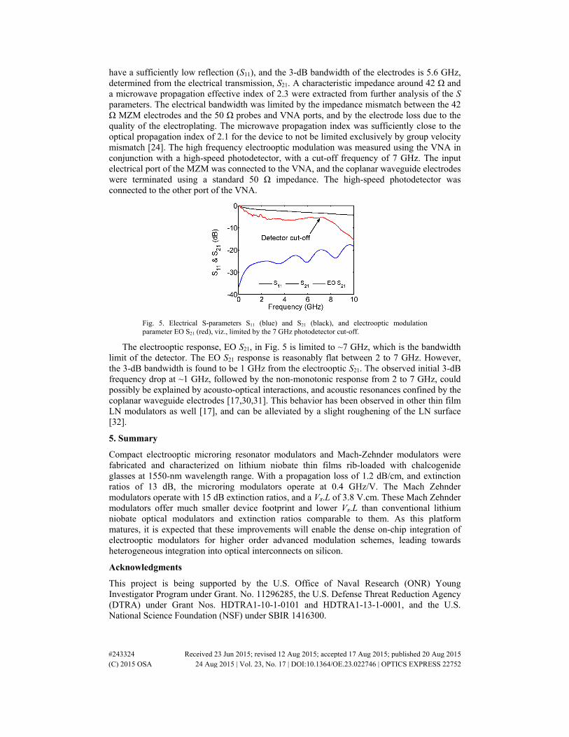
have a sufficiently low reflection (S11), and the 3-dB bandwidth of the electrodes is 5.6 GHz, determined from the electrical transmission, S21. A characteristic impedance around 42 Ω and a microwave propagation effective index of 2.3 were extracted from further analysis of the S parameters. The electrical bandwidth was limited by the impedance mismatch between the 42 Ω MZM electrodes and the 50 Ω probes and VNA ports, and by the electrode loss due to the quality of the electroplating. The microwave propagation index was sufficiently close to the optical propagation index of 2.1 for the device to not be limited exclusively by group velocity mismatch [24]. The high frequency electrooptic modulation was measured using the VNA in conjunction with a high-speed photodetector, with a cut-off frequency of 7 GHz. The input electrical port of the MZM was connected to the VNA, and the coplanar waveguide electrodes were terminated using a standard 50 Ω impedance. The high-speed photodetector was connected to the other port of the VNA.
Fig. 5. Electrical S-parameters S11 (blue) and S21 (black), and electrooptic modulation parameter EO S21 (red), viz., limited by the 7 GHz photodetector cut-off.
The electrooptic response, EO S21, in Fig. 5 is limited to ~7 GHz, which is the bandwidth limit of the detector. The EO S21 response is reasonably flat between 2 to 7 GHz. However, the 3-dB bandwidth is found to be 1 GHz from the electrooptic S21. The observed initial 3-dB frequency drop at ~1 GHz, followed by the non-monotonic response from 2 to 7 GHz, could possibly be explained by acousto-optical interactions, and acoustic resonances confined by the coplanar waveguide electrodes [17,30,31]. This behavior has been observed in other thin film LN modulators as well [17], and can be alleviated by a slight roughening of the LN surface [32].
5. Summary
Compact electrooptic microring resonator modulators and Mach-Zehnder modulators were fabricated and characterized on lithium niobate thin films rib-loaded with chalcogenide glasses at 1550-nm wavelength range. With a propagation loss of 1.2 dB/cm, and extinction ratios of 13 dB, the microring modulators operate at 0.4 GHz/V. The Mach Zehnder modulators operate with 15 dB extinction ratios, and a Vπ.L of 3.8 V.cm. These Mach Zehnder modulators offer much smaller device footprint and lower Vπ.L than conventional lithium niobate optical modulators and extinction ratios comparable to them. As this platform matures, it is expected that these improvements will enable the dense on-chip integration of electrooptic modulators for higher order advanced modulation schemes, leading towards heterogeneous integration into optical interconnects on silicon.
Acknowledgments
This project is being supported by the U.S. Office of Naval Research (ONR) Young Investigator Program under Grant. No. 11296285, the U.S. Defense Threat Reduction Agency (DTRA) under Grant Nos. HDTRA1-10-1-0101 and HDTRA1-13-1-0001, and the U.S. National Science Foundation (NSF) under SBIR 1416300.
#243324 Received 23 Jun 2015; revised 12 Aug 2015; accepted 17 Aug 2015; published 20 Aug 2015 (C) 2015 OSA 24 Aug 2015 | Vol. 23, No. 17 | DOI:10.1364/OE.23.022746 | OPTICS EXPRESS 22752

![Single-Sideband OFDM Transmission via a Silicon Microring ... · External modulators [4], such as dual-drive Mach-Zehnder This work is supported by Fonds de Recherche du Qubec-Nature](https://static.fdocuments.net/doc/165x107/606b61789e245253d40fa0dc/single-sideband-ofdm-transmission-via-a-silicon-microring-external-modulators.jpg)