Transistor and their Characteristics – Lesson-1 Junction Transistor
HETERO JUNCTION FIELD EFFECT TRANSISTOR
NE3210S01X to Ku BAND SUPER LOW NOISE AMPLIFER
N-CHANNEL HJ-FET
Document No. P14067EJ2V0DS00 (2nd edition)Date Published November 1999 N CP(K)
DATA SHEET
The mark shows major revised points.
DESCRIPTIONThe NE3210S01 is a Hetero Junction FET that utilizes the hetero junction to create high mobility electrons. Its
excellent low noise and associated gain make it suitable for DBS and another commercial systems.
FEATURES• Super Low Noise Figure & High Associated Gain
NF = 0.35 dB TYP. Ga = 13.5 dB TYP. at f = 12 GHz
• Gate Length: Lg ≤ 0.20 µm
• Gate Width : Wg = 160 µm
ORDERING INFORMATION (PLAN)
Part Number Supplying Form Marking
NE3210S01-T1 Tape & reel 1 000 pcs./reel
NE3210S01-T1B Tape & reel 4 000 pcs./reel
K
Remark For sample order, please contact your nearby sales office. (Part number for sample order: NE3210S01-A)
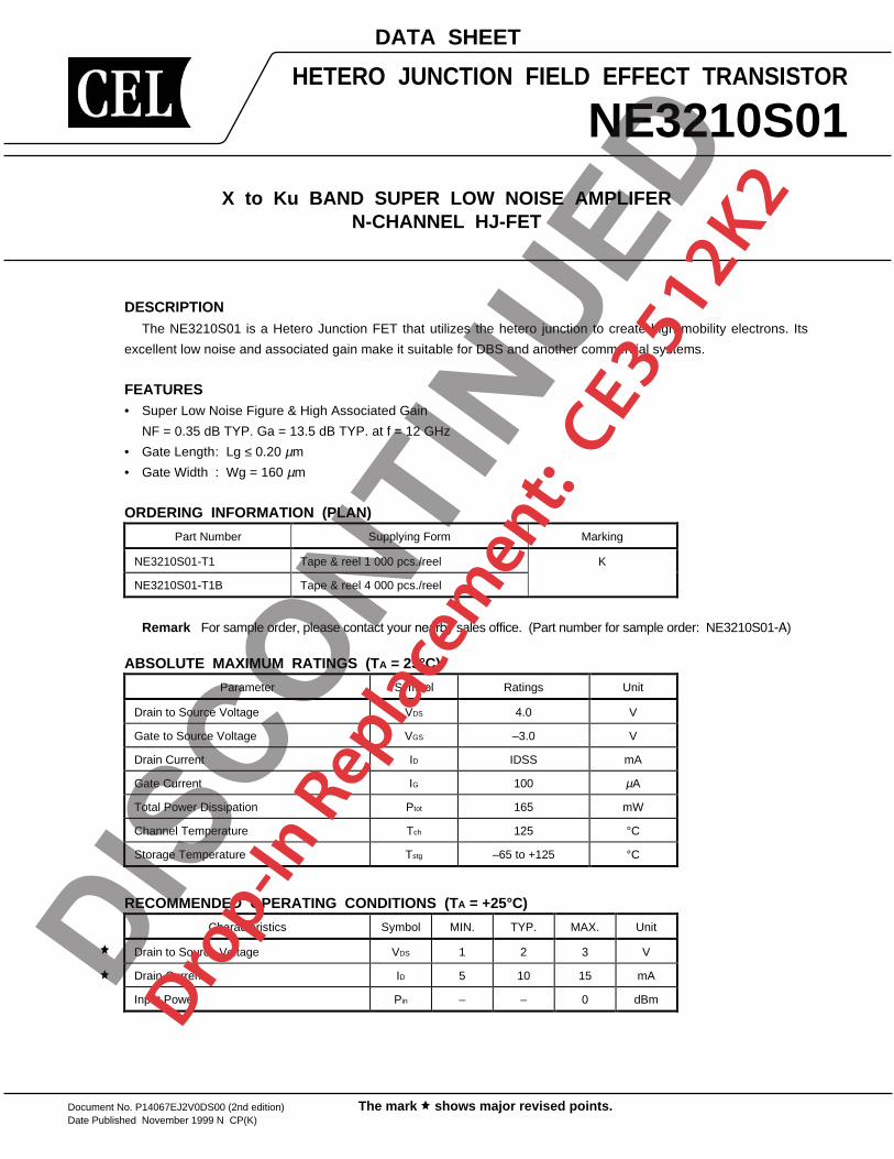
ABSOLUTE MAXIMUM RATINGS (T A = 25°C)
Parameter Symbol Ratings Unit
Drain to Source Voltage VDS 4.0 V
Gate to Source Voltage VGS –3.0 V
Drain Current ID IDSS mA
Gate Current IG 100 µA
Total Power Dissipation Ptot 165 mW
Channel Temperature Tch 125 °C
Storage Temperature Tstg –65 to +125 °C
RECOMMENDED OPERATING CONDITIONS (TA = +25°C)
Characteristics Symbol MIN. TYP. MAX. Unit
Drain to Source Voltage VDS 1 2 3 V
Drain Current ID 5 10 15 mA
Input Power Pin – – 0 dBm
DISCONTI
NUED
Drop-In
Rep
lace
men
t: CE3512K2
Data Sheet P14067EJ2V0DS002
NE3210S01
ELECTRICAL CHARACTERISTICS (T A = +25 °C)
Characteristics Symbol Test Conditions MIN. TYP. MAX. Unit
Gate to Source Leak Current IGSO VGS = –3 V – 0.5 10 µA
Saturated Drain Current IDSS VDS = 2 V, VGS = 0 V 15 40 70 mA
Gate to Source Cut off Voltage VGS (off) VDS = 2 V, IDS = 100 µA –0.2 –0.7 –2.0 V
Transconductance gm VDS = 2 V, IDS = 10 mA 40 55 – mS
Noise Figure NF – 0.35 0.45 dB
Associated Gain Ga
VDS = 2 V, IDS = 10 mA
f = 12 GHz12.0 13.5 – dB
DISCONTI
NUED
Drop-In
Rep
lace
men
t: CE3512K2
Data Sheet P14067EJ2V0DS00 3
NE3210S01
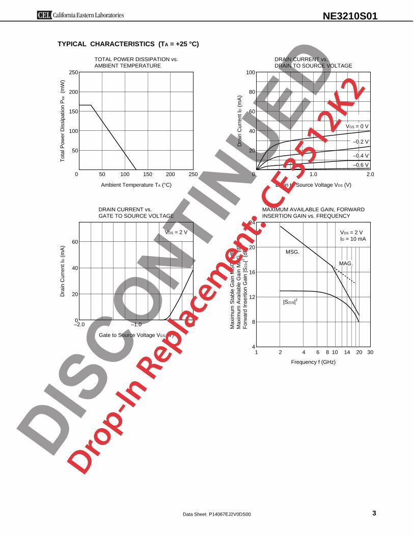
TYPICAL CHARACTERISTICS (T A = +25 °C)
250
200
150
100
50
0 50 100 150 200 250
TOTAL POWER DISSIPATION vs.AMBIENT TEMPERATURE
Ambient Temperature TA (°C)
Tot
al P
ower
Dis
sipa
tion
Pto
t (m
W)
DRAIN CURRENT vs.DRAIN TO SOURCE VOLTAGE
Drain to Source Voltage VDS (V)
100
80
60
40
20
0 2.01.0
Dra
in C
urre
nt ID
(m
A)
VGS = 0 V
–0.2 V
–0.4 V
–0.6 V
60
40
20
0–2.0 –1.0 0
DRAIN CURRENT vs.GATE TO SOURCE VOLTAGE
Gate to Source Voltage VGS (V)
Dra
in C
urre
nt ID
(m
A)
Frequency f (GHz)
Max
imum
Sta
ble
Gai
n M
SG
. (dB
)M
axim
um A
vaila
ble
Gai
n M
AG
. (dB
)F
orw
ard
Inse
rtio
n G
ain
|S21
s|2 (dB
)
VDS = 2 V
MAXIMUM AVAILABLE GAIN, FORWARDINSERTION GAIN vs. FREQUENCY
24
20
16
12
8
41 302 4 206 8 10 14
VDS = 2 VID = 10 mA
MSG.
MAG.
|S21S|2
DISCONTI
NUED
Drop-In
Rep
lace
men
t: CE3512K2
Data Sheet P14067EJ2V0DS004
NE3210S01
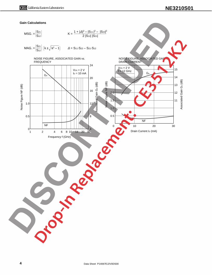
Gain Calculations
S21MAG. =
S12k ± k2 – 1 = S11·S22 – S21·S12
S21MSG. =
S12
1 + | |2 – |S11 |2 – |S22|2K =
2 |S12| |S21|∆
∆
Frequency f (GHz)
1.0
0.5
01 302
Noi
se F
igur
e N
F (
dB)
VDS = 2 VID = 10 mA
4 206 8 10 14
24
20
16
12
8
4
Ass
ocia
ted
Gai
n G
a (d
B)
Noi
se F
igur
e N
F (
dB)
Ass
ocia
ted
Gai
n G
a (d
B)
Drain Current ID (mA)
Ga
NF
Ga
NF
NOISE FIGURE, ASSOCIATED GAIN vs.DRAIN CURRENT
15
14
13
12
11
2.0
1.5
1.0
0.5
3020100
VDS = 2 Vf = 12 GHz
NOISE FIGURE, ASSOCIATED GAIN vs.FREQUENCY
DISCONTI
NUED
Drop-In
Rep
lace
men
t: CE3512K2

Data Sheet P14067EJ2V0DS00 5
NE3210S01
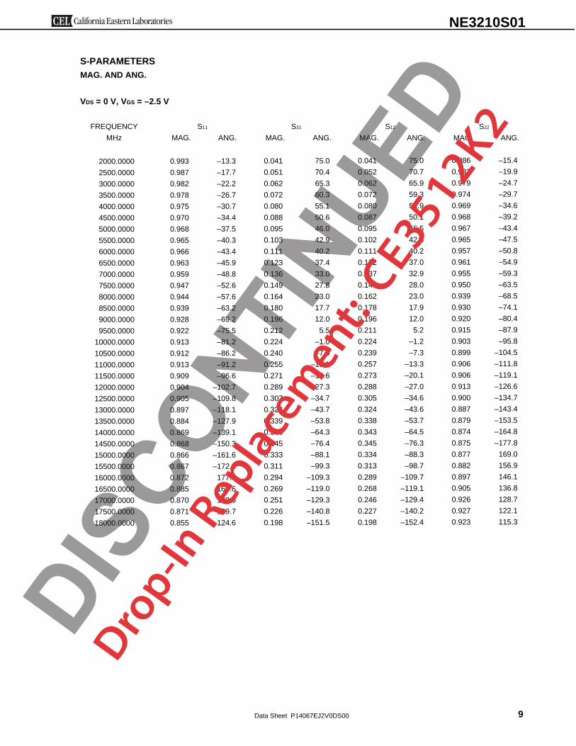
S-PARAMETERSMAG. AND ANG.
VDS = 2 V, ID = 10 mA
FREQUENCY S11 S21 S12 S22
MHz MAG. ANG. MAG. ANG. MAG. ANG. MAG. ANG.
2000.0000
2500.0000
3000.0000
3500.0000
4000.0000
4500.0000
5000.0000
5500.0000
6000.0000
6500.0000
7000.0000
7500.0000
8000.0000
8500.0000
9000.0000
9500.0000
10000.0000
10500.0000
11000.0000
11500.0000
12000.0000
12500.0000
13000.0000
13500.0000
14000.0000
14500.0000
15000.0000
15500.0000
16000.0000
16500.0000
17000.0000
17500.0000
18000.0000
0.973
0.951
0.935
0.914
0.893
0.872
0.848
0.829
0.814
0.781
0.745
0.699
0.660
0.635
0.602
0.578
0.554
0.537
0.507
0.477
0.445
0.428
0.418
0.430
0.453
0.486
0.513
0.526
0.531
0.539
0.533
0.537
0.546
–21.2
–27.7
–34.3
–40.6
–46.3
–51.4
–55.9
–60.0
–64.8
–70.1
–76.3
–82.7
–90.3
–99.8
–109.5
–118.3
–127.2
–135.2
–144.1
–154.0
–166.2
–179.6
165.3
150.6
137.9
126.7
116.7
108.4
100.4
91.1
82.1
72.2
64.7
4.450
4.453
4.439
4.389
4.314
4.230
4.158
4.118
4.130
4.149
4.180
4.170
4.184
4.197
4.171
4.109
4.063
4.030
3.978
3.950
3.906
3.851
3.762
3.642
3.517
3.395
3.259
3.150
3.046
2.911
2.739
2.573
2.400
154.2
147.1
140.3
133.5
127.3
121.1
115.3
109.9
104.3
98.3
91.8
85.3
78.7
71.7
64.7
57.9
51.3
44.6
37.6
30.8
23.5
16.0
8.5
1.1
–6.1
–13.0
–19.9
–26.4
–33.3
–40.7
–48.0
–54.3
–59.4
0.022
0.028
0.033
0.038
0.042
0.045
0.048
0.050
0.053
0.058
0.063
0.065
0.070
0.074
0.077
0.081
0.086
0.092
0.095
0.099
0.103
0.108
0.110
0.111
0.110
0.112
0.111
0.113
0.110
0.112
0.111
0.110
0.106
75.9
71.2
66.7
63.5
57.7
54.5
49.7
48.2
46.1
42.8
40.4
36.6
33.7
29.4
25.4
22.3
18.9
15.3
10.8
5.9
2.1
–2.2
–6.6
–10.3
–14.8
–19.6
–22.0
–25.6
–29.3
–32.1
–36.1
–40.1
–41.6
0.550
0.538
0.523
0.511
0.500
0.495
0.492
0.484
0.482
0.472
0.450
0.423
0.393
0.360
0.327
0.290
0.268
0.251
0.233
0.224
0.211
0.187
0.157
0.123
0.110
0.125
0.161
0.207
0.255
0.299
0.329
0.343
0.347
–15.2
–19.9
–25.2
–30.3
–34.9
–39.1
–42.9
–45.8
–48.8
–52.6
–56.3
–59.2
–62.6
–67.3
–72.4
–78.8
–86.8
–96.2
–105.3
–114.3
–123.1
–132.5
–146.2
–164.0
169.0
141.4
121.7
113.4
109.0
105.4
101.5
95.9
90.6
DISCONTI
NUED
Drop-In
Rep
lace
men
t: CE3512K2
Data Sheet P14067EJ2V0DS006
NE3210S01
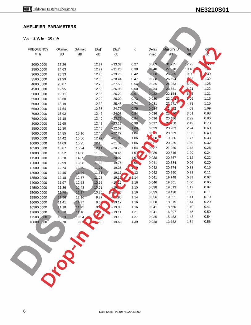
AMPLIFIER PARAMETERS
VDS = 2 V, ID = 10 mA
FREQUENCY GUmax GAmax |S21|2 |S12|2 K Delay Mason’s U G1 G2
MHz dB dB dB dB nsec dB dB dB
2000.0000
2500.0000
3000.0000
3500.0000
4000.0000
4500.0000
5000.0000
5500.0000
6000.0000
6500.0000
7000.0000
7500.0000
8000.0000
8500.0000
9000.0000
9500.0000
10000.0000
10500.0000
11000.0000
11500.0000
12000.0000
12500.0000
13000.0000
13500.0000
14000.0000
14500.0000
15000.0000
15500.0000
16000.0000
16500.0000
17000.0000
17500.0000
18000.0000
27.26
24.63
23.33
21.99
20.87
19.95
19.11
18.50
18.19
17.54
16.92
16.18
15.65
15.30
14.85
14.42
14.09
13.87
13.52
13.28
12.99
12.74
12.45
12.18
11.97
11.86
11.70
11.56
11.41
11.18
10.70
10.23
9.70
16.16
15.56
15.25
15.24
14.66
14.39
13.98
13.69
13.26
12.87
12.58
12.48
12.27
12.16
11.97
11.75
11.16
10.54
9.85
12.97
12.97
12.95
12.85
12.70
12.53
12.38
12.29
12.32
12.36
12.42
12.40
12.43
12.46
12.40
12.27
12.18
12.11
11.99
11.93
11.83
11.71
11.51
11.23
10.92
10.62
10.26
9.97
9.67
9.28
8.75
8.21
7.60
–33.03
–31.20
–29.75
–28.44
–27.53
–26.98
–26.29
–26.00
–25.48
–24.70
–24.08
–23.76
–23.13
–22.59
–22.22
–21.80
–21.32
–20.75
–20.46
–20.07
–19.76
–19.35
–19.17
–19.12
–19.15
–19.02
–19.06
–18.90
–19.17
–19.03
–19.11
–19.15
–19.53
0.27
0.38
0.42
0.47
0.54
0.60
0.67
0.73
0.74
0.79
0.84
0.94
0.98
1.00
1.04
1.06
1.06
1.04
1.07
1.07
1.09
1.09
1.12
1.14
1.16
1.15
1.16
1.14
1.16
1.16
1.21
1.27
1.39
0.389
0.040
0.038
0.038
0.035
0.034
0.032
0.030
0.031
0.034
0.036
0.036
0.037
0.039
0.039
0.038
0.037
0.037
0.039
0.038
0.041
0.042
0.042
0.041
0.040
0.038
0.039
0.036
0.038
0.041
0.041
0.035
0.028
31.735
27.870
26.985
26.594
24.253
23.581
22.154
22.043
22.571
21.992
21.786
20.486
20.250
20.283
20.009
19.986
20.235
21.050
20.646
20.667
20.584
20.774
20.290
19.748
19.301
19.613
19.428
19.651
18.875
18.560
16.897
15.483
13.782
12.72
10.18
9.00
7.83
6.92
6.21
5.53
5.05
4.73
4.09
3.51
2.92
2.49
2.24
1.96
1.77
1.59
1.48
1.29
1.12
0.96
0.88
0.83
0.89
1.00
1.17
1.33
1.41
1.44
1.49
1.45
1.48
1.54
1.56
1.48
1.39
1.32
1.25
1.22
1.21
1.16
1.15
1.09
0.98
0.86
0.73
0.60
0.49
0.38
0.32
0.28
0.24
0.22
0.20
0.15
0.11
0.07
0.05
0.07
0.11
0.19
0.29
0.41
0.50
0.54
0.56
DISCONTI
NUED
Drop-In
Rep
lace
men
t: CE3512K2

Data Sheet P14067EJ2V0DS00 7
NE3210S01
S-PARAMETERSMAG. AND ANG.
VDS = 0 V, VGS = 0 V
FREQUENCY S11 S21 S12 S22
MHz MAG. ANG. MAG. ANG. MAG. ANG. MAG. ANG.
2000.0000
2500.0000
3000.0000
3500.0000
4000.0000
4500.0000
5000.0000
5500.0000
6000.0000
6500.0000
7000.0000
7500.0000
8000.0000
8500.0000
9000.0000
9500.0000
10000.0000
10500.0000
11000.0000
11500.0000
12000.0000
12500.0000
13000.0000
13500.0000
14000.0000
14500.0000
15000.0000
15500.0000
16000.0000
16500.0000
17000.0000
17500.0000
18000.0000
0.987
0.984
0.978
0.973
0.967
0.964
0.959
0.954
0.948
0.944
0.934
0.920
0.906
0.893
0.885
0.877
0.873
0.876
0.874
0.874
0.867
0.870
0.872
0.874
0.884
0.899
0.904
0.907
0.907
0.900
0.881
0.860
0.846
–21.3
–27.9
–34.8
–41.5
–47.7
–53.6
–59.1
–64.8
–70.7
–77.9
–85.5
–95.5
–106.1
–117.9
–129.6
–140.4
–151.4
–162.1
–173.2
174.1
160.1
146.2
132.8
121.0
110.6
101.9
92.9
85.1
77.7
69.3
60.5
52.8
46.0
0.013
0.019
0.024
0.031
0.039
0.048
0.056
0.067
0.077
0.087
0.102
0.117
0.132
0.144
0.155
0.167
0.177
0.190
0.205
0.219
0.228
0.232
0.230
0.227
0.218
0.211
0.208
0.201
0.198
0.198
0.192
0.183
0.176
103.3
103.6
106.2
102.7
99.2
97.3
95.2
90.9
85.9
81.4
76.1
70.0
62.7
55.8
48.4
41.9
35.7
28.8
21.9
13.9
5.1
–4.0
–11.4
–19.4
–26.4
–30.5
–35.0
–39.5
–43.9
–49.3
–54.4
–59.2
–63.5
0.015
0.020
0.026
0.033
0.039
0.048
0.057
0.068
0.079
0.090
0.104
0.118
0.132
0.144
0.158
0.166
0.179
0.193
0.206
0.218
0.229
0.232
0.232
0.227
0.221
0.215
0.208
0.201
0.200
0.198
0.194
0.186
0.176
109.1
102.3
106.6
105.2
101.9
99.3
94.9
90.9
86.8
81.4
76.8
70.2
62.9
55.2
48.7
42.2
35.9
29.2
21.4
13.5
5.2
–3.5
–11.6
–19.7
–25.5
–30.6
–35.4
–40.0
–44.0
–49.5
–54.5
–60.2
–63.9
0.775
0.786
0.786
0.787
0.786
0.783
0.782
0.781
0.782
0.781
0.785
0.796
0.802
0.814
0.819
0.830
0.832
0.836
0.838
0.837
0.839
0.838
0.845
0.854
0.862
0.871
0.879
0.882
0.876
0.877
0.878
0.875
0.866
151.9
145.8
140.4
134.6
129.0
123.0
116.4
109.7
103.2
96.6
90.2
84.7
80.4
76.7
73.8
70.7
67.9
64.3
60.7
56.5
52.1
47.3
42.8
38.5
35.9
34.0
33.5
33.0
32.4
30.8
28.5
25.4
21.4
DISCONTI
NUED
Drop-In
Rep
lace
men
t: CE3512K2
Data Sheet P14067EJ2V0DS008
NE3210S01
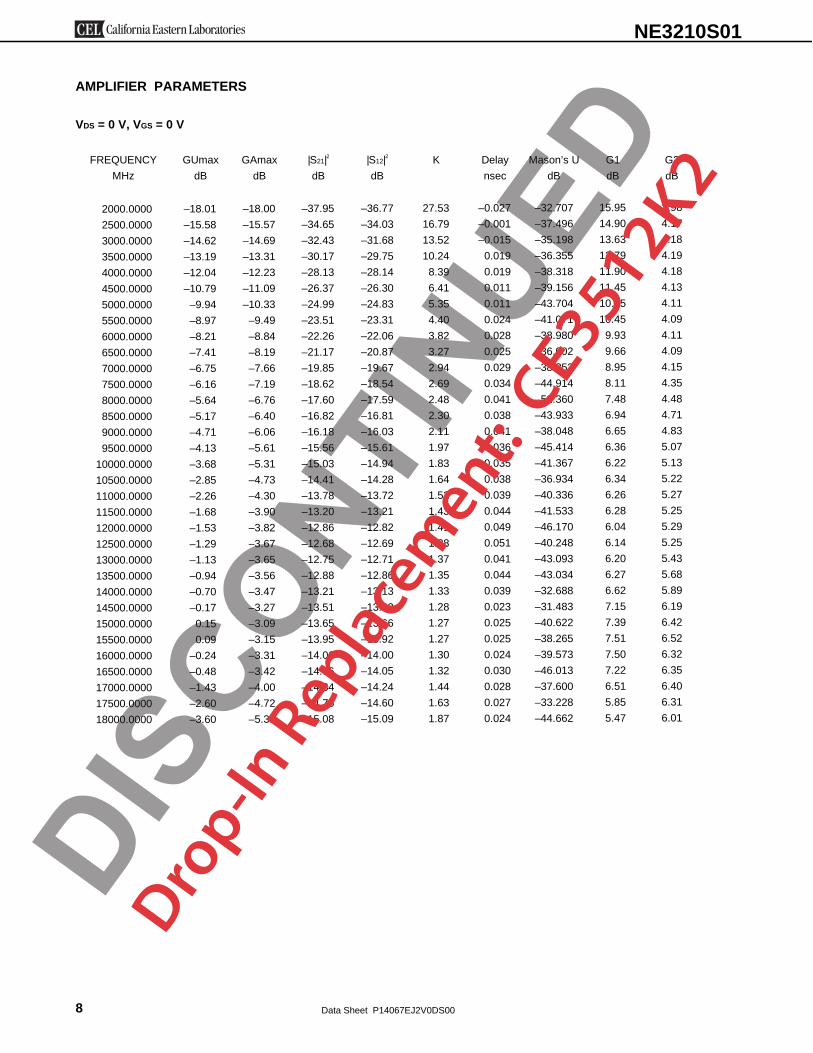
AMPLIFIER PARAMETERS
VDS = 0 V, VGS = 0 V
FREQUENCY GUmax GAmax |S21|2 |S12|2 K Delay Mason’s U G1 G2
MHz dB dB dB dB nsec dB dB dB
2000.0000
2500.0000
3000.0000
3500.0000
4000.0000
4500.0000
5000.0000
5500.0000
6000.0000
6500.0000
7000.0000
7500.0000
8000.0000
8500.0000
9000.0000
9500.0000
10000.0000
10500.0000
11000.0000
11500.0000
12000.0000
12500.0000
13000.0000
13500.0000
14000.0000
14500.0000
15000.0000
15500.0000
16000.0000
16500.0000
17000.0000
17500.0000
18000.0000
–18.01
–15.58
–14.62
–13.19
–12.04
–10.79
–9.94
–8.97
–8.21
–7.41
–6.75
–6.16
–5.64
–5.17
–4.71
–4.13
–3.68
–2.85
–2.26
–1.68
–1.53
–1.29
–1.13
–0.94
–0.70
–0.17
0.15
0.09
–0.24
–0.48
–1.43
–2.60
–3.60
–18.00
–15.57
–14.69
–13.31
–12.23
–11.09
–10.33
–9.49
–8.84
–8.19
–7.66
–7.19
–6.76
–6.40
–6.06
–5.61
–5.31
–4.73
–4.30
–3.90
–3.82
–3.67
–3.65
–3.56
–3.47
–3.27
–3.09
–3.15
–3.31
–3.42
–4.00
–4.72
–5.38
–37.95
–34.65
–32.43
–30.17
–28.13
–26.37
–24.99
–23.51
–22.26
–21.17
–19.85
–18.62
–17.60
–16.82
–16.18
–15.56
–15.03
–14.41
–13.78
–13.20
–12.86
–12.68
–12.75
–12.88
–13.21
–13.51
–13.65
–13.95
–14.06
–14.06
–14.34
–14.76
–15.08
–36.77
–34.03
–31.68
–29.75
–28.14
–26.30
–24.83
–23.31
–22.06
–20.87
–19.67
–18.54
–17.59
–16.81
–16.03
–15.61
–14.94
–14.28
–13.72
–13.21
–12.82
–12.69
–12.71
–12.86
–13.13
–13.33
–13.66
–13.92
–14.00
–14.05
–14.24
–14.60
–15.09
27.53
16.79
13.52
10.24
8.39
6.41
5.35
4.40
3.82
3.27
2.94
2.69
2.48
2.30
2.11
1.97
1.83
1.64
1.52
1.43
1.41
1.38
1.37
1.35
1.33
1.28
1.27
1.27
1.30
1.32
1.44
1.63
1.87
–0.027
–0.001
–0.015
0.019
0.019
0.011
0.011
0.024
0.028
0.025
0.029
0.034
0.041
0.038
0.041
0.036
0.035
0.038
0.039
0.044
0.049
0.051
0.041
0.044
0.039
0.023
0.025
0.025
0.024
0.030
0.028
0.027
0.024
–32.707
–37.496
–35.198
–36.355
–38.318
–39.156
–43.704
–41.071
–38.980
–36.002
–38.253
–44.914
–52.360
–43.933
–38.048
–45.414
–41.367
–36.934
–40.336
–41.533
–46.170
–40.248
–43.093
–43.034
–32.688
–31.483
–40.622
–38.265
–39.573
–46.013
–37.600
–33.228
–44.662
15.95
14.90
13.63
12.79
11.90
11.45
10.95
10.45
9.93
9.66
8.95
8.11
7.48
6.94
6.65
6.36
6.22
6.34
6.26
6.28
6.04
6.14
6.20
6.27
6.62
7.15
7.39
7.51
7.50
7.22
6.51
5.85
5.47
3.98
4.17
4.18
4.19
4.18
4.13
4.11
4.09
4.11
4.09
4.15
4.35
4.48
4.71
4.83
5.07
5.13
5.22
5.27
5.25
5.29
5.25
5.43
5.68
5.89
6.19
6.42
6.52
6.32
6.35
6.40
6.31
6.01
DISCONTI
NUED
Drop-In
Rep
lace
men
t: CE3512K2
Data Sheet P14067EJ2V0DS00 9
NE3210S01
S-PARAMETERSMAG. AND ANG.
VDS = 0 V, VGS = –2.5 V
FREQUENCY S11 S21 S12 S22
MHz MAG. ANG. MAG. ANG. MAG. ANG. MAG. ANG.
2000.0000
2500.0000
3000.0000
3500.0000
4000.0000
4500.0000
5000.0000
5500.0000
6000.0000
6500.0000
7000.0000
7500.0000
8000.0000
8500.0000
9000.0000
9500.0000
10000.0000
10500.0000
11000.0000
11500.0000
12000.0000
12500.0000
13000.0000
13500.0000
14000.0000
14500.0000
15000.0000
15500.0000
16000.0000
16500.0000
17000.0000
17500.0000
18000.0000
0.993
0.987
0.982
0.978
0.975
0.970
0.968
0.965
0.966
0.963
0.959
0.947
0.944
0.939
0.928
0.922
0.913
0.912
0.913
0.909
0.904
0.905
0.897
0.884
0.869
0.868
0.866
0.867
0.872
0.885
0.870
0.871
0.855
–13.3
–17.7
–22.2
–26.7
–30.7
–34.4
–37.5
–40.3
–43.4
–45.9
–48.8
–52.6
–57.6
–63.2
–69.2
–75.5
–81.2
–86.2
–91.2
–96.6
–102.7
–109.8
–118.1
–127.9
–139.1
–150.3
–161.6
–172.6
177.4
166.6
153.6
139.7
124.6
0.041
0.051
0.062
0.072
0.080
0.088
0.095
0.103
0.111
0.123
0.136
0.149
0.164
0.180
0.196
0.212
0.224
0.240
0.255
0.271
0.289
0.307
0.324
0.339
0.346
0.345
0.333
0.311
0.294
0.269
0.251
0.226
0.198
75.0
70.4
65.3
60.3
55.1
50.6
46.0
42.9
40.2
37.4
33.0
27.8
23.0
17.7
12.0
5.5
–1.0
–7.0
–13.1
–19.6
–27.3
–34.7
–43.7
–53.8
–64.3
–76.4
–88.1
–99.3
–109.3
–119.0
–129.3
–140.8
–151.5
0.041
0.052
0.062
0.072
0.080
0.087
0.095
0.102
0.111
0.122
0.137
0.148
0.162
0.178
0.196
0.211
0.224
0.239
0.257
0.273
0.288
0.305
0.324
0.338
0.343
0.345
0.334
0.313
0.289
0.268
0.246
0.227
0.198
75.0
70.7
65.9
59.3
54.9
50.1
46.5
42.5
40.2
37.0
32.9
28.0
23.0
17.9
12.0
5.2
–1.2
–7.3
–13.3
–20.1
–27.0
–34.6
–43.6
–53.7
–64.5
–76.3
–88.3
–98.7
–109.7
–119.1
–129.4
–140.2
–152.4
0.986
0.982
0.979
0.974
0.969
0.968
0.967
0.965
0.957
0.961
0.955
0.950
0.939
0.930
0.920
0.915
0.903
0.899
0.906
0.906
0.913
0.900
0.887
0.879
0.874
0.875
0.877
0.882
0.897
0.905
0.926
0.927
0.923
–15.4
–19.9
–24.7
–29.7
–34.6
–39.2
–43.4
–47.5
–50.8
–54.9
–59.3
–63.5
–68.5
–74.1
–80.4
–87.9
–95.8
–104.5
–111.8
–119.1
–126.6
–134.7
–143.4
–153.5
–164.8
–177.8
169.0
156.9
146.1
136.8
128.7
122.1
115.3
DISCONTI
NUED
Drop-In
Rep
lace
men
t: CE3512K2

Data Sheet P14067EJ2V0DS0010
NE3210S01
AMPLIFIER PARAMETERS
VDS = 0 V, VGS = –2.5 V
FREQUENCY GUmax GAmax |S21|2 |S12|2 K Delay Mason’s U G1 G2
MHz dB dB dB dB nsec dB dB dB
2000.0000
2500.0000
3000.0000
3500.0000
4000.0000
4500.0000
5000.0000
5500.0000
6000.0000
6500.0000
7000.0000
7500.0000
8000.0000
8500.0000
9000.0000
9500.0000
10000.0000
10500.0000
11000.0000
11500.0000
12000.0000
12500.0000
13000.0000
13500.0000
14000.0000
14500.0000
15000.0000
15500.0000
16000.0000
16500.0000
17000.0000
17500.0000
18000.0000
6.59
4.66
4.16
3.77
3.27
3.06
3.35
3.47
3.33
4.33
4.16
3.50
3.26
3.09
2.57
2.64
2.13
2.50
3.39
3.74
4.38
4.37
4.00
3.67
3.15
3.16
2.83
2.44
2.65
2.64
2.61
1.77
–0.05
–1.81
–2.29
–2.37
–2.45
–2.57
–2.59
–2.46
–2.35
–2.41
–2.04
–2.07
–2.14
–2.14
–2.15
–2.31
–2.21
–2.37
–2.17
–1.82
–1.63
–1.32
–1.23
–1.27
–1.30
–1.46
–1.48
–1.66
–1.92
–1.85
–2.01
–1.99
–2.46
–3.35
–27.69
–25.78
–24.10
–22.90
–21.96
–21.12
–20.43
–19.76
–19.10
–18.22
–17.36
–16.54
–15.68
–14.91
–14.16
–13.47
–13.01
–12.40
–11.86
–11.33
–10.79
–10.26
–9.79
–9.38
–9.22
–9.24
–9.54
–10.14
–10.64
–11.41
–12.01
–12.90
–14.05
–27.72
–25.76
–24.15
–22.89
–21.97
–21.17
–20.42
–19.86
–19.12
–18.27
–17.24
–16.59
–15.80
–15.00
–14.16
–13.52
–13.00
–12.44
–11.80
–11.29
–10.80
–10.32
–9.78
–9.42
–9.30
–9.24
–9.52
–10.09
–10.80
–11.43
–12.17
–12.88
–14.06
1.09
1.14
1.16
1.16
1.18
1.19
1.16
1.16
1.16
1.12
1.11
1.13
1.13
1.13
1.14
1.13
1.15
1.13
1.09
1.07
1.05
1.04
1.04
1.05
1.06
1.06
1.07
1.10
1.10
1.11
1.12
1.16
1.31
0.037
0.026
0.028
0.027
0.029
0.025
0.026
0.017
0.015
0.015
0.025
0.029
0.026
0.030
0.032
0.036
0.036
0.033
0.034
0.036
0.043
0.041
0.050
0.056
0.059
0.067
0.065
0.062
0.055
0.054
0.057
0.064
0.059
–41.579
–37.612
–32.931
–30.070
–46.684
–36.484
–36.357
–32.225
–46.847
–34.379
–30.925
–37.284
–31.894
–33.177
–60.851
–37.108
–47.342
–36.990
–33.577
–31.606
–33.886
–33.321
–40.261
–36.338
–31.349
–48.824
–38.005
–31.130
–27.440
–47.034
–28.001
–33.848
–33.797
18.66
15.91
14.46
13.70
13.12
12.23
11.96
11.57
11.70
11.37
10.93
9.90
9.67
9.30
8.60
8.25
7.79
7.72
7.81
7.62
7.37
7.42
7.08
6.61
6.12
6.09
6.02
6.05
6.21
6.65
6.14
6.18
5.71
15.62
14.53
13.79
12.97
12.12
11.95
11.82
11.66
10.73
11.18
10.58
10.14
9.28
8.70
8.13
7.87
7.36
7.18
7.45
7.45
7.79
7.22
6.71
6.44
6.25
6.31
6.35
6.53
7.08
7.40
8.48
8.49
8.29
DISCONTI
NUED
Drop-In
Rep
lace
men
t: CE3512K2
Data Sheet P14067EJ2V0DS00 11
NE3210S01
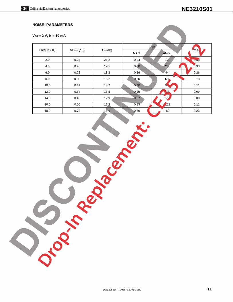
NOISE PARAMETERS
VDS = 2 V, ID = 10 mA
ΓoptFreq. (GHz) NFmin. (dB) Ga (dB)
MAG. ANG.Rn/50
2.0 0.25 21.2 0.94 12 0.38
4.0 0.26 19.5 0.80 26 0.33
6.0 0.28 18.2 0.66 44 0.26
8.0 0.30 16.2 0.50 68 0.18
10.0 0.32 14.7 0.38 97 0.11
12.0 0.34 13.5 0.29 133 0.09
14.0 0.42 12.9 0.27 177 0.08
16.0 0.56 12.3 0.33 –129 0.11
18.0 0.72 11.9 0.39 –82 0.23
DISCONTI
NUED
Drop-In
Rep
lace
men
t: CE3512K2
Data Sheet P14067EJ2V0DS0012
NE3210S01
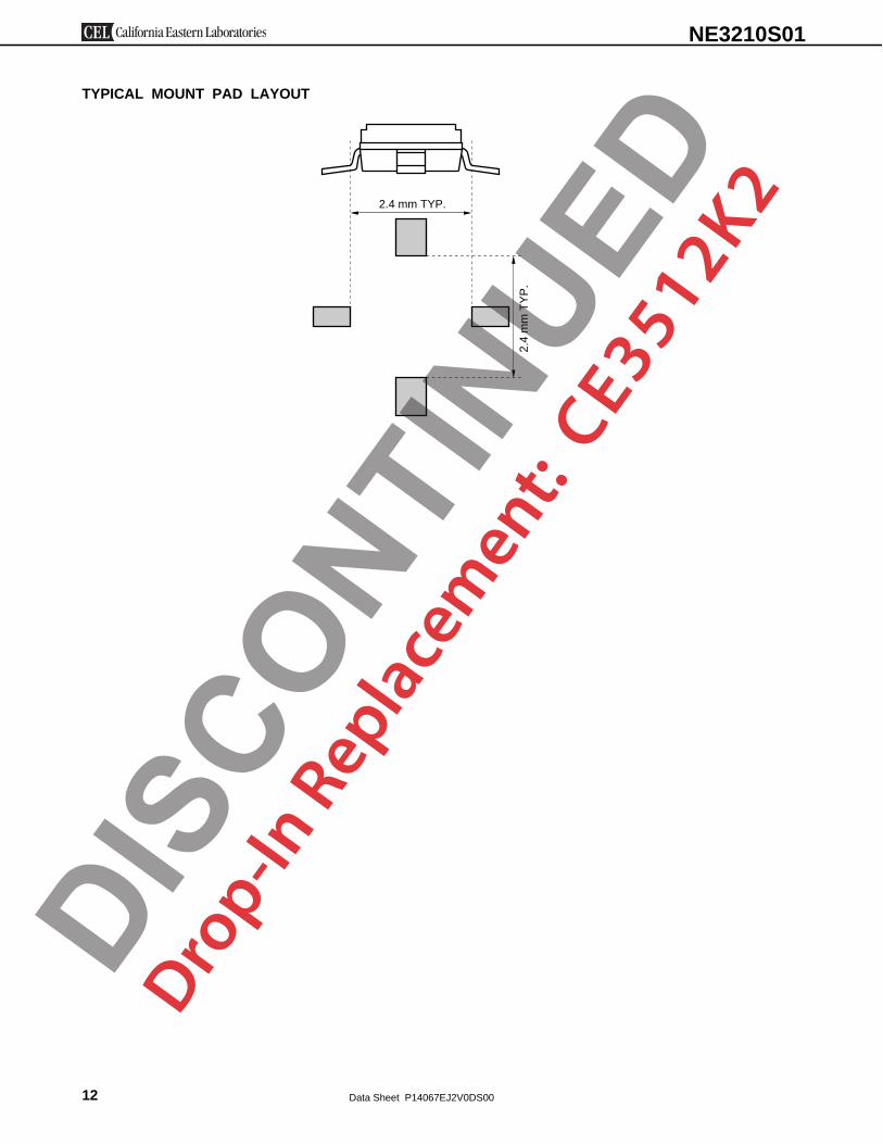
TYPICAL MOUNT PAD LAYOUT
2.4 mm TYP.
2.4
mm
TY
P.
DISCONTI
NUED
Drop-In
Rep
lace
men
t: CE3512K2
Data Sheet P14067EJ2V0DS00 13
NE3210S01
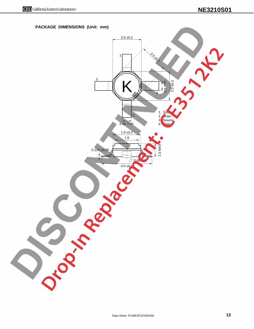
PACKAGE DIMENSIONS (Unit: mm)
0.5
TY
P.
2.0
±0.2
4
0.65 TYP.
3
2
1
2.0 ±0.2
2.0 ±0.2
K
1.9 ±0.2
1.6
4.0 ±0.2
0.125 ±0.05
1.5
MA
X0.4MAX
1. Source2. Drain3. Source4. Gate
DISCONTI
NUED
Drop-In
Rep
lace
men
t: CE3512K2
Data Sheet P14067EJ2V0DS0014
NE3210S01
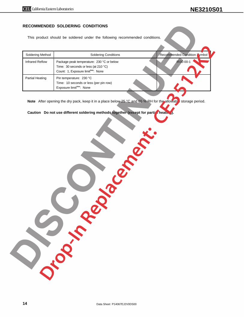
RECOMMENDED SOLDERING CONDITIONS
This product should be soldered under the following recommended conditions.
Soldering Method Soldering Conditions Recommended Condition Symbol
Infrared Reflow Package peak temperature: 230 °C or below
Time: 30 seconds or less (at 210 °C)
Count: 1, Exposure limitNote: None
IR30-00-1
Partial Heating Pin temperature: 230 °C
Time: 10 seconds or less (per pin row)
Exposure limitNote: None
–
Note After opening the dry pack, keep it in a place below 25 °C and 65 % RH for the allowable storage period.
Caution Do not use different soldering methods together (except for partial heating).
DISCONTI
NUED
Drop-In
Rep
lace
men
t: CE3512K2
NOTICE
1. Descriptions of circuits, software and other related information in this document are provided only to illustrate the operation of semiconductor products andapplication examples. You are fully responsible for the incorporation of these circuits, software, and information in the design of your equipment. CaliforniaEastern Laboratories and Renesas Electronics assumes no responsibility for any losses incurred by you or third parties arising from the use of these circuits, software, or information.
2. California Eastern Laboratories has used reasonable care in preparing the information included in this document, but California Eastern Laboratories doesnot warrant that such information is error free. California Eastern Laboratories and Renesas Electronics assumes no liability whatsoever for any damagesincurred by you resulting from errors in or omissions from the information included herein.
3. California Eastern Laboratories and Renesas Electronics do not assume any liability for infringement of patents, copyrights, or other intellectual propertyrights of third parties by or arising from the use of Renesas Electronics products or technical information described in this document. No license, express,implied or otherwise, is granted hereby under any patents, copyrights or other intellectual property rights of California Eastern Laboratories or RenesasElectronics or others.
4. You should not alter, modify, copy, or otherwise misappropriate any Renesas Electronics product, whether in whole or in part. California EasternLaboratories and Renesas Electronics assume no responsibility for any losses incurred by you or third parties arising from such alteration, modification, copyor otherwise misappropriation of Renesas Electronics product.
5. Renesas Electronics products are classified according to the following two quality grades: “Standard” and “High Quality”. The recommended applicationsfor each Renesas Electronics product depends on the product’s quality grade, as indicated below. “Standard”: Computers; office equipment; communicationsequipment; test and measurement equipment; audio and visual equipment; home electronic appliances; machine tools; personal electronic equipment; and industrial robots etc. “High Quality”: Transportation equipment (automobiles, trains, ships, etc.); traffic control systems; anti-disaster systems; anti-crime systems; and safety equipment etc. Renesas Electronics products are neither intended nor authorized for use in products or systems that may pose a direct threat to human life or bodily injury (artificial life support devices or systems, surgical implantations etc.), or may cause serious property damages (nuclearreactor control systems, military equipment etc.). You must check the quality grade of each Renesas Electronics product before using it in a particularapplication. You may not use any Renesas Electronics product for any application for which it is not intended. California Eastern Laboratories and RenesasElectronics shall not be in any way liable for any damages or losses incurred by you or third parties arising from the use of any Renesas Electronics productfor which the product is not intended by California Eastern Laboratories or Renesas Electronics.
6. You should use the Renesas Electronics products described in this document within the range specified by California Eastern Laboratories, especially with respect to the maximum rating, operating supply voltage range, movement power voltage range, heat radiation characteristics, installation and other productcharacteristics. California Eastern Laboratories shall have no liability for malfunctions or damages arising out of the use of Renesas Electronics productsbeyond such specified ranges.
7. Although Renesas Electronics endeavors to improve the quality and reliability of its products, semiconductor products have specific characteristics such as the occurrence of failure at a certain rate and malfunctions under certain use conditions. Further, Renesas Electronics products are not subject to radiationresistance design. Please be sure to implement safety measures to guard them against the possibility of physical injury, and injury or damage caused by fire in the event of the failure of a Renesas Electronics product, such as safety design for hardware and software including but not limited to redundancy, fire control and malfunction prevention, appropriate treatment for aging degradation or any other appropriate measures. Because the evaluation ofmicrocomputer software alone is very difficult, please evaluate the safety of the final products or systems manufactured by you.
8. Please contact a California Eastern Laboratories sales office for details as to environmental matters such as the environmental compatibility of each Renesas Electronics product. Please use Renesas Electronics products in compliance with all applicable laws and regulations that regulate the inclusion or use of controlled substances, including without limitation, the EU RoHS Directive. California Eastern Laboratories and Renesas Electronics assume no liability for damages or losses occurring as a result of your noncompliance with applicable laws and regulations.
9. Renesas Electronics products and technology may not be used for or incorporated into any products or systems whose manufacture, use, or sale is prohibited under any applicable domestic or foreign laws or regulations. You should not use Renesas Electronics products or technology described in this document for any purpose relating to military applications or use by the military, including but not limited to the development of weapons of mass destruction. Whenexporting the Renesas Electronics products or technology described in this document, you should comply with the applicable export control laws and regulations and follow the procedures required by such laws and regulations.
10. It is the responsibility of the buyer or distributor of California Eastern Laboratories, who distributes, disposes of, or otherwise places the Renesas Electronicsproduct with a third party, to notify such third party in advance of the contents and conditions set forth in this document, California Eastern Laboratories andRenesas Electronics assume no responsibility for any losses incurred by you or third parties as a result of unauthorized use of Renesas Electronics products.
11. This document may not be reproduced or duplicated in any form, in whole or in part, without prior written consent of California Eastern Laboratories.12. Please contact a California Eastern Laboratories sales office if you have any questions regarding the information contained in this document or Renesas
Electronics products, or if you have any other inquiries.
NOTE 1: “Renesas Electronics” as used in this document means Renesas Electronics Corporation and also includes its majority-owned subsidiaries.NOTE 2: “Renesas Electronics product(s)” means any product developed or manufactured by or for Renesas Electronics.NOTE 3: Products and product information are subject to change without notice.
CEL Headquarters • 4590 Patrick Henry Drive, Santa Clara, CA 95054 • Phone (408) 919-2500 • www.cel.com
For a complete list of sales offices, representatives and distributors,Please visit our website: www.cel.com/contactusDISCONTI
NUED
Drop-In
Rep
lace
men
t: CE3512K2