
Hello and welcome to the 3rd Generation HF Packerfredsforum.nl/pdf/HFPackerAmp3.227113959.pdfMay 26,...
49
HF PROJECTS - K5OOR - Virgil Stamps Web: www.hfprojects.com Email: [email protected] Cell: 281-4679424 Fax: 214 242-5080 Address: 5802 Miller Valley Drive Houston, TX 77066 Hello and welcome to the 3rd Generation HF Packer- Amp Home Construction Project. This is version 3 of the popular HF Packer-Amp. Significant changes to improve construction have been incorporated in this revision. I went through and revised the artworks for the HF Packer-Amp. The changes are primarily to fix part foot prints and to improve the silk screen lettering. Everything is backwards compatible with the existing HF Packer-Amp. The goal is to make everything go together more smoothly. Here is a list of the improvements: Rev 2 Amplifier board changes • Improved Silkscreen and circuit board routing • Now using a 3rd generation design relay used in the SuperPacker Pro • Added a jack for an external switch to change the T/R hold time for CW or SSB (optional - add user supplied toggle switch and wires mounted on the rear panel). • Added 10-turn pots to set the bias current. This change removes the sensitivity of a 1-turn pot. PSU Rev 3 board changes • Improved Silkscreen and circuit board routing • Added 5V local regulator so the PSU may be tested without being attached to the amp board. • Changed spacing on 1uH inductor • Improved routing to eliminate potential shorts to standoffs. • 3-pin Header now the proper length (no modification required). LowPass Filter board changes • Improved Silkscreen and circuit board routing • Increased size slightly and improved part placement • Corrected parts spacing and better placement identification Case • The case has been re-tooled for an excellent fit and a dazzling finish! Construction Manual • Restructured layout to provide a section for each module and a final assembly steps with more photos. Get in on the HF (Having Fun) Projects experience with this 3rd generation. Happy Building! 73 K5OOR - Virgil
Transcript of Hello and welcome to the 3rd Generation HF Packerfredsforum.nl/pdf/HFPackerAmp3.227113959.pdfMay 26,...

HF PROJECTS - K5OOR - Virgil Stamps
Web: www.hfprojects.com Email: [email protected] Cell: 281-4679424 Fax: 214 242-5080 Address: 5802 Miller Valley Drive Houston, TX 77066
Hello and welcome to the 3rd Generation HF Packer-Amp Home Construction Project. This is version 3 of the popular HF Packer-Amp. Significant changes to improve construction have been incorporated in this revision. I went through and revised the artworks for the HF Packer-Amp. The changes are primarily to fix part foot prints and to improve the silk screen lettering. Everything is backwards compatible with the existing HF Packer-Amp. The goal is to make everything go together more smoothly. Here is a list of the improvements:
Rev 2 Amplifier board changes • Improved Silkscreen and circuit board routing • Now using a 3rd generation design relay used in the SuperPacker
Pro • Added a jack for an external switch to change the T/R hold time
for CW or SSB (optional - add user supplied toggle switch and wires mounted on the rear panel).
• Added 10-turn pots to set the bias current. This change removes the sensitivity of a 1-turn pot.
PSU Rev 3 board changes • Improved Silkscreen and circuit board routing • Added 5V local regulator so the PSU may be tested without being
attached to the amp board. • Changed spacing on 1uH inductor • Improved routing to eliminate potential shorts to standoffs. • 3-pin Header now the proper length (no modification required).
LowPass Filter board changes • Improved Silkscreen and circuit board routing • Increased size slightly and improved part placement • Corrected parts spacing and better placement identification
Case • The case has been re-tooled for an excellent fit and a dazzling
finish!
Construction Manual • Restructured layout to provide a section for each module and a
final assembly steps with more photos. Get in on the HF (Having Fun) Projects experience with this 3rd generation. Happy Building! 73 K5OOR - Virgil

Hfpacker–Amp Rev 2 Assembly
HFpacker-Amp 1
(Manual version: May 26, 2007)
Virgil Stamps K5OOR

IntroductionWelcome all builders to the homebrew Hfpacker-Amp Project.This project parts and your efforts will eventually provide you witha compact 2.5 watt input to 35 watt output linear amplifier for usewith QRP SSB/CW transmitters on the amateur bands 160 through10 meters and which can be powered from a 12 volt DC supply. Inthis section, you are building the Amplifier Module. The design isa good balance between output power, physical size and batterypower consumption. The completed amplifier will reward thebuilder with a clean, more powerful output signal for a QRP rigwhen radio conditions become marginal.
This project is not a beginner's project and requires a medium skilllevel to complete it successfully. Builders require soldering, handtool, basic electronics and component identification skills. Thisproject manual is not included with the kit in order to keep kit coststo a minimum. All builders will thus require Internet access todownload this PDF document file fromhttp://www.hfprojects.com. The manual is produced in landscapeformat to allow more readable text per screen. This manualprovides all you will need to successfully complete the amplifierproject, however, some additional PDF files are provided at theabove website for those interested in seeing more pictures of theproject at various stages of construction.
The genesis of this circuit is fully described in the 2001 ARRLHandbook and in reprint articles from the ARRL. If you are anARRL member, you can view the amplifier articles on-line at:http://www.arrl.org/members-only/tis/info/pdf/9903040.pdf andhttp://www.arrl.org/members-only/tis/info/pdf/9903043.pdf. Fulldesign credit is given to Mike Kossor, WA2EBY. The amplifiermodule is mounted to the inside bottom of the chassis box and itsMOSFETs are attached to a heat sink. The power supply board is
fastened above the amplifier board, while the filter board ismounted vertically along one side end of the chassis.
Circuit Details
The amplifier module is a push-pull design, biased for Class ABlinear operation and uses low-cost power MOSFETs in its outputstage. Maximum efficiency is at 10 MHz and develops over 70watts output. QRP transmitter RF input is first sensed, which tripsa relay, feeding RF through an RF attenuator pad. The signal isthen applied to the primary of T3 via an input impedance-matchingnet- work consisting of L2. T3 is a 1:1 balun that splits the RFsignal into two outputs 180 degrees out of phase. One of thesesignals is applied by C3 to Q1's gate. The other signal is routed viaC8 to Q2's gate. The drains of Q1 and Q2 are connected to theprimary of output transformer T1, where the two signals arerecombined in phase to produce a single output. T1 also providesimpedance transformation from the low output impedance of theMOSFETs to the 50Ω antenna port. DC power is provided to thedrains of Q1 and Q2 by phase-reversal choke, T2. This is a veryeffective method to provide power to Q1 and Q2 while presenting ahigh impedance to the RF signal over a broad range of frequencies.The drain chokes for Q1 and Q2 are wound on the same core, andthe phase of one of the chokes is reversed. C7 increases thebandwidth of impedance transformation provided by T1, especiallyat 21 MHz. The 5 V bias supply voltage is derived from a 78L05regulator. Bypass capacitors C5, C6, C10 and C11 remove RFvoltages from the bias supply voltage. Gate bias for Q1 and Q2 iscontrolled independently. VR1 adjusts Q1's gate-bias voltage viaR1 and L1. VR2 works similarly for Q2 via R5 and L3. At lowfrequencies, the amplifier's input impedance is essentially equal tothe series value of R1 and R5. L1 and L3 improve the input-impedance match at higher frequencies. The low value of seriesresistance provided by R1 and R5 also reduces the Q.
HFpacker-Amp 2

The switch-mode power supply module plugs into the top of theamplifier board and boosts the nominal 13.6VDC input to 24VDCat 4-5 amperes during voice peaks. The power supply is normallyoff unless commanded to be on by the TR Relay, which senses RF,so that during receive or standby its standby current is very low.There is an approximate 7 mA current draw when power supply isoff, 66 mA current draw when power supply is on and 3-10Acurrent draw when the amplifier is keyed by a transceiver.
Performance
The chart shows the typical gain vs frequency you can expect fromthe HF Packer-Amp. The average power out is approximately35W. The fall off in performance at 30MHz is due to the MOSFETcharacteristics. This chart was made with a constant 2.5W input.
PreparationThe most important preparation step before building is to
completely and thoroughly read this section of the manual. Thiswill familiarize you with the circuitry, building requirements and
components.
After reading this document and prior to assembly youshould do an inventory of parts (Appendix A). In the unlikely eventthat you appear to have missing parts, duplicates or wrong partsplease first double check for the parts in all bags, recheck theinventory and if this fails please contact the project organizers.This might also be the time to re-acquaint yourself with how toidentify resistors and capacitors by the standard codings (AppendixE), if you have forgotten.
Construction TechniquesIt is a fact that 90-95% of problems with completed
electronics/radio kits are due to either component misplacement orsoldering faults. We cannot stress highly enough the importance ofdouble checking component installation before soldering and thengood soldering technique in order to have a working amplifier atthe end of this project. Other builder faults are active componentdamage due to over-heating and damage to circuit board pads andtracks caused by poor desoldering, too high a wattage of solderingiron or carelessness. It is very rare to have initially faultycomponents or printed circuit boards (PCBs).
Good Soldering Technique
• use a 12-25 watt soldering iron with a clean, non-corroded,well-tinned, fine tip
• keep the tip clean by frequently rubbing it along a wet sponge• keep the tip tinned• ensure all circuit board pads and component leads are clean (not
a problem with this project because boards and components arenew)
• ensure the soldering iron tip is at its working temperature and is
HFpacker-Amp 3
HF PA POUT TEST #1
0
2
4
6
8
10
12
14
0 5 10 15 20 25 30
F MHz
Gai
n dB
and
Am
ps D
C
DC IGain 1

in contact simultaneously with both surfaces to be soldered (thepad and the component)
• let the contact zones heat before applying only electronics graderosin cored solder (usually 3-6 seconds will do)
• apply the solder to the two surfaces (not the iron tip) and onlyenough solder to coat both surfaces
• ensure that the joint does not move after you remove thesoldering iron tip and until the solder has solidified
• the resultant good solder joint should be shiny, in perfectcontact with pad and wire and often has a concave upwardsappearance
• special care for toroid coils: the toroids and inductors you willwind and solder in this project use enamel coated magnet wire.You must remove this insulation coating at the ends of the wiresprior to soldering. Two techniques are: 1) use a small butanecigarette lighter to burn off the insulation material or 2) take alarge drop of hot solder on your soldering iron tip and run thewire end through the hot solder blob to remove the insulation(this may not work with low wattage irons). Other methods suchas using sandpaper or a razor knife will work but you maydamage the wire or the toroid windings if you are not careful.
Suggested Tools
• 12-25 watt electronics soldering iron, electronics grade solder,iron stand and sponge
• desoldering braid and/or desoldering pump or bulb• fine needle nose pliers, small fine wire cutters, wire stripper• hobby drill and small drill bits,electric drill and drill bits, drill
punch or awl, reamer• drill bits: #60, #43, 1/16, 1/8, 3/16, 1/4, 5/16, 3/8, 5/8, 1” (last
two may be boring bits, punches or reamer) [1.58, 3.18, 4.76,6.35, 7.94, 9.52, 15.88, 25.4mm]
• 4-40 NC size tap with tap handle [M 2.2 x 0.45 1.75mm drill]• small screwdrivers including jewelers screwdrivers, small file• multi-meter, scissors, tape or glue stick, ruler, test leads
• 50 ohm 35 watt dummy load, 50 ohm resistors
Component Installation
For each component, our word “Install” always means:1. Pick the correct part to start with – in the assembly notes that
follow we often provide a part number only. You must matchthis part number with the correct component using the parts lists(Appendix A). Some parts may be in bags other than their ownmodule bags.
2. Insert the component into the correct PCB position. Refer to thePCB component outline (silkscreen) and Appendix D for thefilter module.
3. Orient it correctly, following the PC board outline. This is vitalfor active components, electrolytic and tantalum capacitors anddiodes. Also, it is good practice to mount resistors andcapacitors in identical orientations (for resistors normally readcolor code left to right in same direction as the silkscreen on thePC board). This makes component checks easier.
4. Install all low profile components first: usually resistors,capacitors, diodes, then electrolytics and active components.
5. Resistors should be mounted about 1/8” above the board. 6. Mount all capacitors, relays and connectors as flush to the board
as possible.7. Bend the wires of the components at the bottom side slightly
outwards in order to hold the component in place for soldering.8. Solder as per techniques described above.9. Trim excess wire leads. 10.Mark off each installation step in sequence as you complete it,
in the box provided (e.g. ).11.Warnings and important points are posted with a symbol.
Care of the IRF-510 MOSFET's
HFpacker-Amp 4

MOSFETs are susceptible to electrostatic discharge damage(ESD). It is important to use proper grounding techniques whilehandling the amp circuit board and the MOSFETs in particular.While working with MOSFETs you should wear a grounding strapand have an antistatic mat at your feet. At the very least you shouldfrequently ground your hands to the nearest ground point. TheIRF510 is a good compromise MOSFET that will work up to 30MHz but has poor thermal characteristics of 3.5°C/Watt. Whenused in intermittent SSB and CW service forced-air cooling is notrequired. Tuning time with full power should be limited to less
than 30 seconds with 1-2 minutes between cycles to preventoverheating. Operating at 24VDC does not press the MOSFET totheir limits. The Sil-Pad TO220 mounting kit has excellent thermalperformance and provides a greaseless thermal interface betweenthe MOSFET and the heatsink. Users report that this amplifier canbe safely used for contest CW operation without further cooling.For PSK/RTTY forced air cooling is necessary or a reduction ofpower by reducing the input drive.
HFpacker-Amp 5

.
MOSFET Amplifier Module Board Assembly
Install resistors R1 through R7.__R1 __R5: 27Ω, ½ W (red, viol, blk) __R2: 24Ω, 3 W (red, yel, blk)__R3 __ R4: 220Ω, 3W (red, red, brn)__R6: 1.2K, ¼ W (brn, red, red)__R7: 4.7K, ¼ W (ylw, viol, red)
Install ceramic disc capacitors C1, C3, C4, C5, C6, C8, C9, C10and C11 (all 0.1 uF (104)).__C1 __C3 __C4 __C5 __C6__C8 __C9 __C10 __C11
Install C14 (0.01uF, 103). Install C12 and C15 (.001uF, 102). Install C7 (47pF). Install C2, a radial electrolytic capacitor (106). This cap is
polarized. Insert + lead in the square pad at C2 outline on. The +lead is longest.
Install dip molded capacitor C13 (0.68uF), also polarized. Install dip molded capacitor C16 (1.5uF), also polarized. Install diodes D1 and D3 (1N4148). The black ring on the diode
is the cathode. Form the diode leads with approximately 3/16-inchlead on each side of the body. Use a pair of needle-nose pliers andmake a 90- degree bend. The white line on the PCB outline is thecathode end. D3 needs to be mounted towards the edge of theboard to clear the connector jack J4, installed later.
Install diode D2 (1N4004). The cathode band on the diodealigns with the white stripe of the component outline.
Install the multi-turn potentiometers VR1 and VR2. A littlecircle indicates where the adjustment screw is located..
Using a small bladed screwdriver, turn both pots fullycounter-clockwise. This will be the starting position whenadjusting the MOSFET transistor bias later. Fully counter-clockwise places the wiper of the potentiometer at ground or zerobias voltage.
Install K1. Make certain the pins are straight. Two pins on theend of the relay are spaced further apart from the other pins. Orientthe relay to align with the pattern on the board. Insert the relay andensure that all 8 leads are visible on the solder side. Solder onecorner pin making sure relay is flush to the board. Press down onthe relay while quickly re-heating the pin just soldered to ensurerelay is flush to the board. Solder the remaining pins.
Install U1 (78L05). Ensure the flat of the IC matches the flat ofthe component outline. The body of U1 should be spaced about 1/4inch away from the board.
Install J6 (5-pin connector). Ensure connector is flush againstthe board and perpendicular. Solder one pin. Inspect alignment.Re-flow the soldered pin for final position. Solder the remainingpins.
Install J1 (3-pin connector), as above. Install Q3 (2N5809). Spread the leads of the transistor just
slightly to match the hole pattern on the board. Ensure that the flatof the transistor matches the flat of the component outline. Q3should be spaced about 1/4 inch away from the board.
Install TP1, TP2, TP3. Install J2, J3, J4, J5,J7. The locking ramps are identified on the
silkscreen part outlines.
T1 Transformer Construction
T1 has a primary and secondary winding on the BN-43 3312 baluncore (the large 2 hole ferrite core). Use the two #20 AWG Tefloncovered wires to construct T1. See picture below for a photo of acompleted T1.
HFpacker-Amp 6

Prepare two wires. The first primary wire is 7 inch [178 mm]YLW. The second secondary wire is 10 inch [254 mm] WHT. Theprimary will be two loops while the secondary will be three fullloops.
Run the primary wire through first. Make sure to keep the wiresfrom crossing over and unnecessarily blocking the wiring tube.
Run the secondary wires through. Be careful to organize thepath the wire takes so as to not block the wiring path. It mayappear difficult to pass the last wire through the tube but it can bedone. After you complete the windings, you will have primarywires on one end and secondary wires on the other end.
Strip the wires within ¼ inch [6.35mm] of the tube hole. Place the primary wires on the right side of the rectangle near
capacitor C7 on the amplifier PCB. The secondary wires go to theleft side of the rectangle near J2.
Feed the primary wires into the board and pull them up tightinto the holes. You should not have any strands of wires showingwhen you pull the wire tight into the hole. Solder the primarywires.
Feed the secondary wires into the board and pull them up tightinto the holes. A tiny bit of solder right at the very tip end of thestrands will hold them together as you push them through theholes. Solder the secondary wires.
Position the transformer over the T1 outline. The transformer isnow suspended by the four wires and hovering possibly 1/8 inch[3.18 mm] above the board. Press the transformer down to theboard. The leads will hold the transformer in this position.
T2 Transformer Construction Metric conversions: #22 = [0.6452 mm] #24 = [0.5105 mm]T2 uses two stacked FT-50-43 cores and has ten bifilar turns of #22wire.
Measure and cut two #22 wires[0.6542 mm], each 15 inches
Pass the wire through the center of the two cores. Find thecenter of the wire and bend around the cores in a U shape. Holdone half wire set steady and wind the other wire half through thecenter of the cores 4 additional times for a total of 5 times..
Pass the remaining wire end through the center 5 more times.You now have a total of ten (10) turns through the center of thecores.
Equally distribute the windings on the cores. Trim the ends so that only 3/8-inch [9.52 mm] leads remain. Use a butane cigarette lighter, hot blob of solder, sandpaper,
emery board or small file to remove the enamel from the 4 wires.Tin these leads.
Use an ohmmeter to determine the two windings. On theschematic diagram (Appendix C) the first winding is labeled pins 1and 2 (there should be zero ohms reading between pins 1 and 2).
HFpacker-Amp 7
T1 with Yellow Primary, WhiteSecondary

The second winding is labeled pins 3 and 4 (zero ohms readingbetween pins 3 and 4). Make certain the two windings are notshorted. The circuit board has a square pad identifying lead 1 of thetransformer.
Lay the board flat in front of you with T1 at the top. TP1 shouldbe in your upper left corner.
Viewing the windings of T2 orient T2 so the wires run verticallythrough the cores on the board. When oriented in this position, T2will fit the component outline. See Figures below.
With the PCB oriented such that T1 is in the left hand corner thenLead 1 is upper right, with square pad, Lead 2 is lower right, Lead3 is upper left and Lead 4 is lower left.
Put the 4 leads through the board and snug up T2 tight to theboard. Solder. Inspect your joints to make certain that solder flowsonto the wire and into the holes.
T3 Transformer Construction
T3 uses one FT-50-43 core and has ten (10) bifilar turns of #24wire [0.5105 mm].
Measure and cut two #24 wires, each 11 inches [279 mm] long.It is not necessary to twist the wires together. Just keep themtogether.
Wind 10 turns exactly as explained in the section above fortransformer T2.
Equally distribute the windings on the core. Trim these ends sothat only 3/8-inch [9.52 mm] leads remain.
Remove the enamel insulation (see “Soldering Techniques”)from the 4 wire ends. Tin the leads thoroughly.
Use an ohmmeter to determine the two windings. The firstwinding is labeled pins 1 and 2 (there should be a zero ohmsreading between pins 1 and 2). The second winding is labeled pins3 and 4 (zero ohms reading between pins 3 and 4). Make certainthe two windings are not shorted. The circuit board has a square
pad identifying lead 1 of the transformer. Lay the board flat in front of you with T1 at the top. TP1 should
be in your upper left corner. Viewing the windings of T3 now,orient T3 so the wires run vertically through the cores on the board.When oriented in this position, T3 will fit the component outline.
Orient the PCB oriented such that T1 is in the left hand corner:lead 1 is lower left with the square pad, lead 2 is upper left, lead 3is lower right and lead 4 is upper right.
Put the 4 leads through the board and snug up T3 tight to the
board. Solder. Inspect your joints to make certain that solder flowsonto the wire and into the holes. It will take a little more heat toflow pin 3 since it is the ground plane.
HFpacker-Amp 8

Inductors Assembly
NOTE : Frequent questions concerning 10 or 9 1/2 inductor turns are answered in Figure 7. The next series of steps fabricateL1, L2 and L3 using #24 enameled transformer wire. L1 and L3have 9 ½ turns of #24 close wound on a 0.25 inch ID. These twoinductors are identical in size and are formed by wrapping the turnsover the shaft of a ¼ inch drill bit.
Cut two 12 inch [305 mm] lengths of #24 AWG enameledmagnet wire. Wrap each wire around a ¼” [6.35 mm] drill bit shaft
10 times to make two separate inductors. By wrapping the wirearound the shaft 10 times you will get 9 turns. The last turn arcsonly ½ turn before entering the circuit board.
Trim the excess leads to 3/16 inch [4.76 mm]. Burn or scrapethe insulation off the ends of the wires, tin with solder and insertinto the circuit board. The wires poking through on the circuit sideshould be adjusted to protrude only about 1/8 inch [3.18 mm].Solder.
Align the inductors directly over the L1 and L3 outline on theboard using tweezers. The windings should remain close wound.
Cut a 4-inch [101 mm] length of #24 AWG [0.5105 mm]enameled magnet wire. L2 has 3 ½ turns of #24 close wound on a0.19 inch ID [4.83 mm]. Form the inductor by wrapping the turnsover the body of a .187 [4.75 mm] aluminum spacer. Wrap the wirearound the spacer 4 times. Trim the excess leads to 3/16 inch [4.76mm]. Burn or scrape the insulation off the ends of the wires, tinwith solder and insert into the circuit board. Solder.
Adjust the inductor position to be directly over the L2 outline onthe board. The windings should remain close wound.
MOSFET Installation
HFpacker-Amp 9

Be aware that the sensitivity of a MOSFET’s gate makesthem vulnerable to damage by ESD. If possible, use a solderingiron with a grounded tip. It is recommended the builder wear awrist strap and use an anti-static mat. At the very least, you shouldfrequently ground your hands to the nearest ground point.
Attach four .187 x .25 inch [4.75 x 6.35 mm] male/femalespacers temporarily on the bottom side of the circuit board withfour 4-40 [M2.2] nuts. The male/female spacers are in the chassisparts bag.
Install the MOSFET’s under the circuit board. Bend the leads 90degrees up (away from the mounting surface of the MOSFET)about 0.25 inch [5 mm] away from the body. Push the leads upthrough the pads on the circuit board.
Ensure the MOSFET is flat against the bench with the circuitboard sitting on the spacers and flat on top of the bench. Note also,that the thickness of the chassis (0.06 inch) [1.5 mm] needs to beaccounted for. Sandwich the chassis and heat sink together to getthe proper spacing.
Solder the leads from the component side of the board. Do notbend the leads. Trim the leads flush with the board after soldering.
Center the hole in the tab of MOSFET with the access hole onthe circuit board. You can adjust the MOSFET position slightly byplacing the end of small file through the holes to leverage themovement.
The MOSFETs will be secured to the heat sink during final chassisassembly. Alternately, you may mount the MOSFETs to thechassis, bend the leads up and then thread the leads through theholes of the circuit board. You would do this when the amp boardis mounted to the chassis.
HFpacker-Amp 10

Appendix A – Parts Lists
The parts for the Hfpacker-Amp Module are located in one bag for the module assembly.
HFpacker-Amp 11

Appendix A AMPLIFIER MODULE PARTS LISTDesignator Description QTY.
C1, C3, C4, C5, C6, C8, C9, C10, C11 Capacitor, 0.1uF, 100V, 10% 9C2 Capacitor, 10uF, 35V, radial 1C7 Capacitor, 47pF, 500V (470) 1C12, C15 Capacitor, 0.001uF, 50V, 10% 2C13 Capacitor, 0.68uF, 35V 1C16 Capacitor, 1.5uF, 35V 1C14 Capacitor, 0.01uF, 100V, 10% 1D1, D3 Diode, 1N4148 2D2 Diode, 1N4004 1A 400V 1J1 Connector, 3 pin female, 0.2” PPSS-03-01-T-S 1J2, J3, J4, J5,J7 Header, friction lock 2 CKT male, 0.100 5J6 Connector, 5 pin female, SSW-105-02-S-S 1K1 Relay, DPDT 1L1, L3 Coil (to be wound by builder), 9 1/2T #24AWG 0.25 ID 2L2 Coil (to be wound by builder), 3 1/2T #24AWG 0.19 ID 1Misc. Printed circuit board for amp module, Rev 2 1Misc. Wire, #24 AWG magnet wire [0.5105 mm] 60 in.Misc. Wire, #20 AWG [0.8128 mm] teflon covered Yellow (7 inch) 1Misc. Wire, #20 AWG teflon covered White (10 inch) [254 mm] 1Misc. Wire, #22 AWG [0.6452 mm] magnet wire 36 in.Q1, Q2 IRF-510 MOSFET (static sensitive!) 2Q3 Transistor, 2N5089 1R1, R5 Resistor, 27Ω, ½ W (red, viol, blk) 2R2 Resistor, 24Ω, 3W (red, yel, blk) 1R3, R4 Resistor, 220Ω, 3W (red, red, brn) 1R6 Resistor, 1.2K, ¼ W (brn, red, red) 1R7 Resistor, 4.7K, ¼ W (yel, viol, red) 1T1 Core, balun BN-43-3312 (2 holes) 1T2, T3 Core, FT50-43 ferrite 3TP1, TP2, TP3 Test Point, glass bead insulated (white) 3U1 Regulator, LM78L05ACZ, 5 volts 1VR1, VR2 Resistor, variable potentiometer, 10K 2
HFpacker-Amp 12

HFpacker-Amp 13

Appendix E: Resistor and Capacitor Identification
HFpacker-Amp 14
Identifying Capacitors
Small-value fixed capacitors (such as the silver micacapacitors for the filter module) are usually markedwith one, two, or three digits and no decimal point. Ifone or two digits are used, that is always the value inpicofarads (pF). If there are three digits, the third digitis a multiplier. For example, a capacitor marked "330"would be 33 pF (33 with a multiplier of 0). Similarly,"151" would be 150 pF, and "102" would be 1000 pF(or .001 µF). Fixed capacitors with values of 1000 pFor higher often use a decimal point in the value, such as.001 or .02. This is the value in microfarads (µF).

5
5
4
4
3
3
2
2
1
1
D D
C C
B B
A A
84uH
170uH
BN-43-3312 BALUN COREPRI: 2T, SEC: 3T #20TEFLON COVERED WIRE
T2 = 2 STACKED FT-50-4310 BIFILAR TURNS #22
T3 = FT-50-4310 BIFILARTURNS #24
L1 and L39 1/2 T #24CLOSE WOUND0.25 INCHID
3 1/2 T #24CLOSE WOUND0.19 INCH ID
BIAS SET:ADJUST CURRENTTO 10MA QUIESCENTFOR EACH MOSFET
FILTER-A
FILTER-B
ANTENNAXCVR
CONTROL
POWER
INPUT ATTENUATOR TABLEDB R3 R2 R4 IN OUT RIG3 300 18 300 2.0 1 K24 220 24 220 2.5 1 FT-8175 130 43 130 5.0 1 OTHER
HFpacker-Amp K5OORHF AMPLIFIER MODULEWWW.HFPROJECTS.COM
REV 2.0 6/23/2007
SSB
Q1D
Q2D
TUNE
SWV
SWV
VCC
VCC
+BAT
+BAT SWV
+BAT
VCC
VCC
Q2
IRF510
2
1
3
T1
1 3
2 4
T21 3
2 4
T31
3
2
4
L1
L3
C3.1uF
J312
J512
VR210K
13
2
J2
12
VR110K
13
2
R5 27
+
C161.5uF
J7
1 2
C10.1uF
C12.001uF
C4.1uF
C5.1uF
L2
TP2
1
R74.7K
TP1
1
TP3
1
R224 R4
220R3220
Q1IRF510
2
1
3
J4
12
D1
1N4148
D21N4004
+
C210uF
C11.1uF
C1.1uF
+
C130.68uF
C14.01uF
R1 27
D31N4148
C9.1uF
Q32N5089
R61.2K
J1
123
J6
CON5
12345
C15
.001uF
C747 pF
K1
32
4
67
518
C6.1uF
U178L05
1
3
2VIN
GN
D VOUT
C8.1uF

MOSFET AMP BILL OF MATERIALSAmp Version 2 Revise 6/23/2007
ITEM DESCRIPTION QTY MOSFET AMP 1 010-140-500N5-470J Cap, 47 Pf 500V 5% NPO XICON 1 2 010-80-C320C102K5R Cap, .001uF KEMET 50V 10% 2 3 010-581-SR151C103K Cap, .01uF AVX 100V 10% 1 4 010-581-SR201C104K Cap, .1uF AVX 100V 10% 9 5 010-80T350A684K035AT Cap, 0.68 uF 25V 1 6 010-140-MLRL50V10 CAP 10UF 35V 20% RADIAL ELECTROLYTIC 1 7 015-AMP_VER1.0 MOSFET AMP Circuit Board Rev 2 1 8 020-PSS-03-01-T-S Connector 3-pin .2" pitch SAMTEC (modified) 1 9 020 SSW-105-02-S-S Connector, 5-pin SAMTEC 1 10 020-538-22-23-2021 Header .100 K.K. Friction lock 2 CKT Molex 5 11 035-151-201 Test Point, glass bead ins. (white) 3 12 045-FT50-43 Core, FT50-43 3 13 045-BN-43-3312 Balun Core, BN-43-3312 1 14 050-512-LM78L05ACZ 5V Regulator, Fairchild 1 15 070-655-V23079A1003B301 Relay, 12VDC Non-latching Single coil 1 16 075-283-24 Resistor, 24 ohm 3W 1 17 075-293-27 Resistor 27 ohm 1/2W 2 18 075-283-220 Resistor 220 ohm 3W 2 19 075-291-1.2K Resistor 1.2K 1/4W 5% CF 1 20 075-291-4.7K Resistor 4.7K 1/4W 5% CF 1 21 072-T93YA-10K Pot, 10K ohm Sealed 3/8 inch Multi-Turn Trimmer 2 22 080-512-IRF510 MOSFET, TO-220AB N-Ch Power Fairchild 2 23 080-610-2N5089 NPN, 2N5089 (TO92) 1 24 080-512-1N4148 Diode, 1N4148 2 25 080-583-1N4004 Diode, 1N4004 1A 400V DO41 1 26 095-602-5856-100-05 TEF-20 Wire, Teflon covered #20 AWG YEL 7” 27 095-602-5856-100-05 TEF-20 Wire, Teflon covered #20 AWG WHT 10”28 095-566-8051 Wire, #22 AWG magnet wire, Poly-Thermaleze 1-ft 3 29 095-566-8052 Wire, #24 AWG magnet wire, Poly-Thermaleze 1-ft 5 30 010-74-199D351.5 Cap, 1.5 uF 35V 1

HF PROJECTS
HF PACKER-AMPASSEMBLED CABLE SET
7-8-2006HF Packer-Amp construction reliabilitydepends, in large measure, on how wellthe interconnecting devices arefabricated. In many cases the use ofspecial crimping tools are needed but notavailable to the average builder. Thispurchased option provides all the laborintensive fabricated cables required. Allthe connectors are crimped. See figures8 and 9 for detail of a typical connection.The connector parts normally suppliedwith your HF Packer-Amp bags of partsare used to fabricate the cables in thesecable assemblies.
Assembled Items Included inthe Kit:
1. Filter – A: RG174 Cable withconnector to J1 Filter board.
2. Filter – B: RG174 Cable withconnector to J2 Filter board.
3. RF Input: RG174 Cable withfour 23-77 beads and connectorto BNC.
4. Antenna Cable: RG174 cablewith four 23-77 beads, connectorand lug to SO-239.
5. DC Power Input #14 Cable withtwo FT50-43 cores and crimpedconnectors.
6. Switch Cable: #24 Teflon withswitch to J5 (Tune)
7. LED Cable with LED to D4 (redto pin 1)
Figure 1 FILTER - A CABLEConnecting cable between the amplifieroutput and the Filter input.
Figure 2 FILTER - B CABLEConnecting cable between the filteroutput and the T/R Relay input.
Figure 3 RF INPUT CABLEConnecting cable between the BNCconnector and the amplifier input.
Figure 4 ANTENNA CABLEConnecting cable between the Antennaconnector and the T/R Relay output.

Figure 5 DC POWER INPUT CABLEDC Cable with RFI Cores and crimpconnections each end. Red and blackPower Pole housings included.
Figure 6 SWITCH CABLETune/Operate Cable from front panel toPower Supply Module jack.
Figure 7 LED CABLEThe pins are inserted into the 2-pinhousing after the LED is installedthrough the front panel. The cableterminates at a Power Supply Modulejack.
Assembly Detail for a typicalcable connector.
Figure 8 PIG TAIL ASSEMBLYThe RJ174 cable is stripped back 1 inchand the coax shield trimmed. A 1 inchconnection wire is soldered to the shield.
Figure 9 CONNECTOR ASSEMBLYA length of heat shrink tubing is placedover the exposed wire. The pins areinserted into the housing. The coaxcenter wire always go to pin 1 on thecircuit boards.

CHASSIS MODULE BILL OF MATERIALS7/26/2007
ITEM DESCRIPTION QTY CHKCHASSIS ASSEMBLY
1 Finished case – Fabricated, Drilled, Painted and Silk Screened 12 Drilled and Tapped Heat Sink Aavid 646903B04600 13 35-5167-211 Grommet, Rubber 5167-211 14 35-534-8714 Spacer, Threaded Keystone male/female .187x.250 534-8714 45 35-3049K-ND WASHERS/BUSHING #4 X .031 Keystone 3049K-ND 26 35-BER183-ND HEATSINK SIL-PAD 900 TO-220 ADHV BER183-ND 27 35-H781-ND Screw 4-40 x 3/8 PHILLIPS PANHEAD H781-ND 28 35-H216-ND Nut 4-40 H216-ND 39 35-MSPP0404 Pan Head Machine Screw 4-40 x ¼ 610 35-H343-ND Screw 4-40 x 5/16 PHIL PAN 311 35-H236-ND Washer internal tooth 4-40 H236-ND 312 35-WIT-18R Ty-wrap, 4 inch WIT-18R 113 55-450-1017 EAGLE PLASTICS KNOBS BLACK 1.04"D X .62"H 450-1017 114 20-530-CP-1094-AST Connector, BNC Jack w/tabs CP-1094-AST 115 20-510-7350 SO239 Panel Mtg SO-239-1 116 35-543-8403 Standoff, Hex Male/Female Threaded, ¾ inch 217 35-534-2029 Spacer, RND 0.187 x 0.75 inch ALUM (amp Board) 218 35-537-F2 Foot 4

Low Pass Filter ModuleAssembly Project Manual
HFpacker-Amp 1
(Manual version: June 23, 2007)
Virgil Stamps K5OOR
and volunteers

IntroductionWelcome all builders to the homebrew Hfpacker-Amp FilterModule Assembly Project. This project parts and your efforts willeventually provide you with a compact 160-10M Low-pass FilterModule. This is a subset of the HF Packer-Amp HomeConstruction Project supplied for those who build the FilterModule only or in conjunction with the SlimGem Project.
This project is not a beginner's project and requires a medium skilllevel to complete it successfully. Builders require soldering, handtool, basic electronics and component identification skills. Thisproject manual is not included with the kit in order to keep kit coststo a minimum. All builders will thus require Internet access todownload this PDF document file fromhttp://www.hfprojects.com. The manual is produced in landscapeformat to allow more readable text per screen. This manualprovides all you will need to successfully complete the filtermodule assembly, however, some additional PDF files areprovided at the above website for those interested in seeing morepictures of the project at various stages of construction.
Circuit Details
The filter module board attaches to one internal side of the chassiswith a 6 position rotary switch. It has 6 low-pass filters coveringthe amateur bands 160 through 10 meters for bandpass filtering.The design includes 60 meters. These filters suppress harmonicoutput and comply with FCC regulations. Frequency selection ismade using SW4, a 2-pole, 6-position rotary switch.
SpecificationsSize 2.6 x 1.8 x 1.0” (LWD, excluding knob)Weight less than 3 oz.Supply voltage noneFilter Selection 6-position rotary switchFrequencies 160, 80, 60-40, 30-20, 17-15, 12-10 MControl Manual selection by rotary switchInput Coax to J1 (RG174)Indicator Knob position Output Coax to J2 (RG174)Power output (rated) 35 watts 160 – 10 metersDuty cycle Designed for intermittent SSB service
PreparationThe most important preparation step before building is to
completely and thoroughly read this manual. This will familiarizeyou with the project, its circuitry, building requirements andcomponents.
After reading this document and prior to assembly youshould do an inventory of parts (Appendix A). In the unlikely eventthat you appear to have missing parts, duplicates or wrong partsplease first double check for the parts in the bag, recheck theinventory and if this fails please contact the project organizers.
Construction TechniquesIt is a fact that 90-95% of problems with completed
HFpacker-Amp 2

electronics/radio kits are due to either component misplacement orsoldering faults. We cannot stress highly enough the importance ofdouble checking component installation before soldering and thengood soldering technique in order to have a working filter at theend of this project. Other builder faults are damage to circuit boardpads and tracks caused by poor desoldering, too high a wattage ofsoldering iron or carelessness. It is very rare to have initially faultycomponents or printed circuit boards (PCBs).
Good Soldering Technique
• use a 12-25 watt soldering iron with a clean, non-corroded,well-tinned, fine tip
• keep the tip clean by frequently rubbing it along a wet sponge• keep the tip tinned• ensure all circuit board pads and component leads are clean (not
a problem with this project because boards and components arenew)
• ensure the soldering iron tip is at its working temperature and isin contact simultaneously with both surfaces to be soldered (thepad and the component)
• let the contact zones heat before applying only electronics graderosin cored solder (usually 3-6 seconds will do)
• apply the solder to the two surfaces (not the iron tip) and onlyenough solder to coat both surfaces
• ensure that the joint does not move after you remove thesoldering iron tip and until the solder has solidified
• the resultant good solder joint should be shiny, in perfectcontact with pad and wire and often has a concave upwardsappearance
• special care for toroid coils: the toroids and inductors you willwind and solder in this project use enamel coated magnet wire.You must remove this insulation coating at the ends of the wiresprior to soldering. Two techniques are: 1) use a small butanecigarette lighter to burn off the insulation material or 2) take alarge drop of hot solder on your soldering iron tip and run the
wire end through the hot solder blob to remove the insulation(this may not work with low wattage irons). Other methods suchas using sandpaper or a razor knife will work but you maydamage the wire or the toroid windings if you are not careful.
Suggested Tools
• 12-25 watt electronics soldering iron, electronics grade solder,iron stand and sponge
• desoldering braid and/or desoldering pump or bulb• fine needle nose pliers, small fine wire cutters, wire stripper
Component Installation
For each component, our word “Install” always means:1. Pick the correct part to start with – in the assembly notes that
follow we often provide a part number only. You must matchthis part number with the correct component using the parts lists(Appendix A).
2. Insert the component into the correct PCB position. Refer to thePCB component outline (silkscreen) and Appendix D for thefilter module.
3. Orient it correctly, following the PC board outline. 4. Install components in the order listed.5. Mark off each installation step in sequence as you complete it,
in the box provided (e.g. ).6. Warnings and important points are posted with a symbol.
Winding Toroids
To wind a toroidal inductor, pull the correct wire lengththrough the toroid core center, dividing the wire length in half.Wrap half the turns with one wire end and then wrap the remaining
HFpacker-Amp 3

turns with the other end. Each pass through the center of the corecounts as one turn (e.g., in Figure 1 there are 3 turns). Afterwinding, the turns should be evenly spaced around most of thecore, leaving a small (about 30º) gap between the first and lastturns (i.e. about 85% of the circumference of the toroidal coreshould contain evenly spaced wire turns). You must then removethe insulation coating the ends of the two toroid wire ends usingtechniques described above. All coils are started in the directionshown in Figure 1.
Filter Module Board AssemblyThe assembly of the filter module PCB comprises 5 steps:1. wind and prepare all the toroids2. install the silver mica capacitors3. install all the toroids4. install the rotary switch5. perform a continuity test
It is important that the above steps be done in order. It is alsosuggested that the builder refer to Appendix B for toroid andcapacitor placement positions, because the solder pads on thisboard are very close together and components are soldered to bothsides of this PCB. To avoid winding the coils again, wind in thedirection shown in Figure 1.
Toroids Construction Wind L1: cut 16" [381 mm] piece of 24 ga. enameled wire,select BLUE T50-1 core, wind 21 turns. Used on 160 meters.
Wind L2: cut 16" [381 mm] piece of 24 ga. enameled wire,select BLUE T50-1 core, wind 21 turns. Used on 160 meters. Wind L3: cut 11" [228 mm] piece of 24 ga. enameled wire,select RED T50-2 core, wind 10 turns. Used on 30-20 meters. Wind L4: cut 10" [203 mm] piece of 24 ga. enameled wire,select RED T50-2 core, wind 9 turns. Used on 30-20 meters. Wind L5: cut 9" [178 mm] piece of 24 ga. enameled wire, selectRED T50-2 core, wind 8 turns. Used on 30-20 meters. Wind L6: cut 15" [381 mm] piece of 24 ga. enameled wire,select RED T50-2 core, wind 20 turns. Used on 80 meters. Wind L7: cut 15" [381 mm] piece of 24 ga. enameled wire,select RED T50-2 core,. wind 20 turns. Used on 80 meters. Wind L8: cut 10" [279 mm] piece of 24 ga. enameled wire,select BLACK T50-10 core, wind 11 turns. Used on 17/15 meters. Wind L9: cut 10" [254 mm] piece of 24 ga. enameled wire,select BLACK T50-10 core, wind 10 turns. Used on 17-15 meters. Wind L10: cut 13" [330 mm] piece of 24 ga. enameled wire,select RED T50-2 core, wind 15 turns, Used on 60 and 40 meters. Wind L11: cut 12" [330 mm] piece of 24 ga. enameledwire, select RED T50-2 core, wind 13 turns. Used on 60 and 40meters.
Wind L12: cut 9" [254 mm] piece of 24 ga. enameled wire,select BLACK T50-10 core, wind 8 turns. Used on 12-10 meters.
Wind L13: cut 8" [228 mm] piece of 24 ga. enameled wire,
HFpacker-Amp 4

select BLACK T50-10 core, wind 7 turns. Used on 12-10 meters For all toroids:
Verify the # of turns are correct and the windings are evenlyspaced about 80% of the core..
Cut the tail of the toroid leads to about 1/2 inch [12.7 mm]long.
Remove completely the enamel insulation from the leads towithin 1/8 inch [3.18 mm] of the core. Use a butane lighter to burnit off or a blob of hot solder to aid in removal of the enamel, orscrape it off carefully with a file or sandpaper.
Do not yet install these toroid inductors. Installation is afterinstallation of the capacitors on the bottom side of the circuitboard.
Bottom-side Capacitor Assembly
All but three of the silver mica capacitors are installed on thebottom side of the filter PCB. Arrange the capacitors on the tablein the order shown for easy assembly.
Capacitors are installed from top to bottom and from right toleft. Push the capacitor through and flush with the board. Bend theleads at a very slight angle and cut the leads short. Solder one lead,making sure capacitor is still flush with the board and then solderthe other lead. Trim the residual leads short as possible.
Install in order :__C23 330 pF (330) __C13 1200 pF (1200) __C9 220 pF (220) __C17 220 pF (220)__C8 220 pF (220) __C14 12 pF (12) __C2 150 pF (150) __C1 27 pF (27)
__C28 110 pF (110)__C19 10 pF (10) __C16 150 pF (150) __C24 82 pF (82)__C7 100 pF (100) __C25 150 pF (150)__ C27 39 pF (39) __C26 68 pF (68) __C20 33 pF (33)__C10 47 pF (47) __C3 120 pF (120) __C15 39 pF (39) __C18 100 pF (100) __C12 1800 pF (1800) __C11 1200 pF (1200) __C21 390 pF (390) __C22 680 pF (680)
Top-side Toroid Assembly
Figure 9 is a photo of the toroids and some capacitors mounted onthe top layer of the filter module circuit board. Appendix D alsohas a good parts placement diagram. The builder should refer toboth in order to assist in correct toroid installation. In order toremove excess toroid leads in confined areas where wire cutterscannot be positioned properly grasp the end of the soldered toroidlead with long-nose pliers. Slowly bend the lead back and forthuntil it breaks off.
Install toroids in the following order, proceed from left to rightand from top to bottom along the PCB:__L3 (red, 10 turns) 0.63 uH__L4 (red, 9 turns) 0.48 uH__L8 (black, 11 turns) 0.47 uH__L2 (blue, 21 turns) 5.08 uH
HFpacker-Amp 5
__L12 (black, 8 turns) 0.47 uH__L7 (red, 20 turns) 2.51 uH__L11 (red, 13 turns) 1.17 uH__L10 (red, 15 turns) 1.37 uH (Solder top side)__L6 (red, 20 turns) 2.51 uH (Solder top side)__L1 (blue, 21 turns) 5.08 uH__L13 (black, 7 turns) 0.26 uH__L9 (black, 10 turns) 0.43 uH__L5 (red, 8 turns) 0.43 uH
Install the remaining silver mica capacitors on the top layer: __C5 2700 pF (2700) __C6 1500 pF (1500) __C4 1500 pF (1500) Clip 1 lead to 1/8 inch. Solder cap side whilepressing cap lead into hole.
Rotary Switch Installation A small rectangle on the component outline for SW4 identifies
how the switch is to be aligned for insertion. The key (plastic tip)should align with this rectangle of the component outline.
Mount SW4 to the circuit board. Space the board away from theswitch body such that the tips of the switch just come through thecircuit board. This will provide the proper spacing between theinductors and a chassis. Make sure the board is parallel with thefront panel.
You can remove and discard the internal tooth washer on theswitch but do not disturb the position of the switch keying tab onthe shaft of the switch. This is the switch locking device set for a 2-pole 6-position switch.
Toroid Continuity/Short Tests
In this section we will use an ohmmeter to assure the builderof toroid continuity and that there are no shorts to ground on thetoroids, which could destroy Q1 and Q2 amplifier MOSFETs whenthe amplifier is powered up.
Connect multimeter between J1, pin 1 and J2, pin 1 on filterboard. Zero ohms must be read as SW4 (the rotary band switch) isswitched through all 6 positions.
If your meter does not read zero ohms, check the filterschematic to see which toroids are installed in that particularswitch position. Re-flow the associated toroid solder joints, orremove and re-work that toroid.
Connect multimeter between pins 1 and 2 of J1 on filter board.There should be no reading, i.e. No shorts to ground as SW4 isrotated through its 6 positions. Any shorts must be repaired/
Connecting Cables A 10 inch coax cable is connected to J2. Attach to the capacitor
side of the circuit board. The center conductor connects to pin 1.
A 4 inch coax cable is connected to J1. Attach to the capacitorside of the circuit board. The center conductor connects to pin 1.
HFpacker-Amp 6

Appendix A – Parts Lists
HFpacker-Amp 7

Appendix A FILTER MODULE PARTS LISTDesignator Description QTY.
C1 Capacitor, 27pF, 500V, silver mica 1C2, C16, C25 Capacitor, 150pF, 500V, silver mica 3C20 Capacitor, 33pF, 500V, silver mica 1C3 Capacitor, 120pF, 500V, silver mica 1C4, C6 Capacitor, 1500pF, 500V, silver mica 2C5 Capacitor, 2700pF, 500V, silver mica 1C7, C18 Capacitor, 100pF, 500V, silver mica 2C8, C9, C17 Capacitor, 220pF, 500V, silver mica 3C10 Capacitor, 47pF, 500V, silver mica 1C23 Capacitor, 330pF, 500V, silver mica 1C22 Capacitor, 680pF, 500V, silver mica 1C21 Capacitor, 390pF, 500V, silver mica 1C28 Capacitor, 110pF, 500V, silver mica 1C11, C13 Capacitor, 1200pF, 500V, silver mica 2C12 Capacitor, 1800pF, 500V, silver mica 1C14 Capacitor, 12pF, 500V, silver mica 1C15, C27 Capacitor, 39pF, 500V, silver mica 2C19 Capacitor, 10pF, 500V, silver mica 1C24 Capacitor, 82pF, 500V, silver mica 1C26 Capacitor, 68pF, 500V, silver mica 1L1, L2 Toroid core, T50-1 (blue) 2L3, L4, L5, L6, L7, L10, L11 Toroid core, T50-2 (red) 7L8, L9, L12, L13 Toroid core, T50-10 (black) 4Misc. Printed circuit board for filter module Rev 2 1Misc. Wire, #24 AWG magnet wire 15.0'SW4 Switch, rotary, 6 position, 10WA175 1
HFpacker-Amp 8
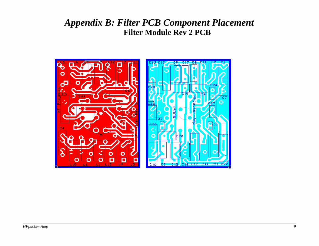
Appendix B: Filter PCB Component PlacementFilter Module Rev 2 PCB
HFpacker-Amp 9

5
5
4
4
3
3
2
2
1
1
D D
C C
B B
A A
160
80
60/40
30/20
17/15
12/10
BAND
HFpacker-Amp Filter Module Rev 2HF Projects by K5OOR 2007
B40
A80
A160 B160
B80
A40
A1715
B3020A3020
B1715
B1210A1210
A40
A30
20
B16
0
B30
20
A17
15
A16
0
B40
A80
B17
15
A12
10
B12
10
B80
SW4SW 2P-6W 10WA175
A2 3
6
4 589
1
1011
12 7
C
C2150pF
C127pF
C2739pF
C28110pF
J2
FILTER-B
1 2J1
FILTER-A
1 2
C17220pF
L8 .47uH
C18100pF
L9 .43uH
C16150pF
C3120pF
L5 .43uHL4 .48uH
C7100pF
C1047pF
L3 .63uH
C8220pF
C9220pF
C22680pF
C2033pF
L2 5.08uH
C61500pF
L1 5.08uH
C41500pF
C52700pF
C121800pF
L7 2.51uH
C131200pF
L6 2.51uH
C111200pF
C1539pF
C1412pF
L11 1.17uHL10 1.37uH
C23330pF
C21390pF
C2482pF
L12 .32uH L13 .26uH
C1910pF
C25150pF
C2668pF


FILTER MODULE BILL OF MATERIALS REV 26/22/2007
ITEM DESCRIPTION QTY CHK1 10-5982-10-500V10 Cap, 10 pF C19 12 10-5982-10-500V12 Cap, 12 pF C14 13 10-5982-10-500V27 Cap, 27 pF C1 14 10-5982-10-500V33 Cap, 33 pF, C20 15 10-5982-10-500V39 Cap, 39 pF C15, C27 26 10-5982-10-500V47 Cap, 47 pF C10 17 10-5982-10-500V110 Cap, 110 pF C28 18 10-5982-15-500V68 Cap, 68 pF C26 19 10-5982-15-500V82 Cap, 82 pF C24 110 10-5982-10-500V100 Cap, 100pF C7, C18 211 10-5982-15-500V120 Cap, 120 pF C3 112 10-5982-10-500V150 Cap, 150 pF C2, C16, C25 313 10-5982-15-500v220 Cap, 220 Pf C8, C9, C17 314 10-5982-15-500V330 Cap, 330 pF C23 115 10-5982-15-500V390 Cap, 390 pF C21 116 10-5982-19-500V680 Cap, 680 pF C22 117 10-5982-19-500V1200 Cap, 1200 pF C11, C13 218 10-5982-19-500V1500 Cap, 1500 pF C4, C6 219 10-5982-19-500V1800 Cap, 1800 pF C12 120 10-5982-19-500V2700 Cap, 2700 pF C5 121 15-FilterModuleRev2 Circuit Board REV 2 122 45-T50-1 Toroid T50-1 (BLUE) L1, L2 223 45-T50-2 Toroid T50-2 (RED) L3, L4, L5, L6, L7, L10, L11 724 45-T50-10 Toroid T50-10 (BLACK) L8, L9, L12, L13 425 85-10WA175 Switch, Rotary, SW4 126 95-566-8052 Wire, #24 AWG magnet wire, Poly-Thermaleze 1 ft 15'

PSU REV 3
HF PROJECTS

PSU REV 3
HF PROJECTS

Power Supply Module Board Assembly
The Power Supply Unit (PSU) Rev 3 develops 24V with a maximum current of 5A from a 12VDCsupply. The PSU is controlled by the signal on pin 2 of J4. Grounding this pin activates the powersupply. A two pin test header (J6) is provided for test purposes to manually turn the PSU on duringcheckout. U1 is a switching regulator. U2 is a switch and over-current shutoff device. If currentexceeds 5A, the U2 part will heat up and thermally open circuit the connection to the J3 connector(load). It is an auto-reset device. The purpose is to provide short-circuit protection for U1.
This version includes a local 5V regulator. Refer to the picture, parts layout, bill of materials andschematic to aid in assembly.
Install all resistors:__R2: 1.0Ω ¼ W (brn, blk, gold)__R3 __R9 __R12 __R15: 4.7K ¼ W (ylw, viol, red)__R4 __R14: 22K ¼ W (red, red, org)__R5 __R8: 100K ¼ W (brn, blk, ylw)__R6 __R7: 1.2K ¼ W (brn, red, red)__R16: 2.7K ¼ W (red, viol, red)
Install four 0.1uF capacitors __C6, __C7, __C10, __C11 Install one 1.0uF capacitors__C8, Observe the lead with the stripe identifying the + lead.. Insert the
+ lead in the hole with the + symbol (square pad). Install two 0.47uF capacitors__C24, __C25. Observe the lead with the stripe identifying the + lead.
Insert the + lead in the hole with the + symbol (square pad).
Install Dl (RL251). The silver band of the diode aligns with the white stripe of the componentoutline.It is ok to stand this part and 1/8th inch above the board surface.
Install __D3, __D5 (1N4148). The black bands of the diodes align with the white stripe of thecomponent outline.
Install __D6, __D7 (1N753A). The color bands of these zener diodes align with the white stripe ofthe component outline. The zener is slightly larger than the 1N4148 diode. The two zener diodes areattached to a tape strip and have a Z written on the tape.
Install inductor L2 , 1.0 uH
Install U1. This part requires that the leads be formed in a specific way. It is advisable to work on astatic free pad with a ground strap to your wrist. You will note that the leads are pre-bent in a staggerconfiguration for vertical mounting. However, we are going to mount the device flush against theboard. The first step is to straighten the leads so they are all flat. Holding the tab in one hand and with apair on needle-nose pliers in the other, squeeze the five leads about ¼ inch from the body. All 5 leadsshould now be flat. Hold U1 near its PCB outline position. Notice that leads 2 and 4 will have a shorterbend than leads 1, 3 and 5. A recessed dimple marks pin 1 on the device that will go into the square padhole. Pins 2 and 4 are bent at a right-angle 1/8 inch [3.18 mm] from the body. Temporarily place thepart on the board with pins 2 and 4 through the board. Observe where pins 1, 3 and 5 need to be bent togo through their pads. Insert the 5 leads through the holes.

Place 4-40 screw [M2.2] from the backside through the board and through the tab of the device.Place an internal tooth washer over the threads. Fasten a 4-40 nut [M2.2] and tighten the component tothe board. Make certain while tightening that the body is flush against the board and that the leads arenot under strain when in final position. The leads should be parallel with the device and then downthrough the board. It is only necessary to trim leads 2 and 4 on the backside so that all 5 lead tips stickslightly through the board. An insulating shoulder washer is not needed for the screw since thepotential of the tab and the board is ground. Solder.
Install TP1, TP2, TP3, TP4. Orient the wire of the test points in the same direction for consistency. Install CB1 (Thermal Circuit Breaker- a yellow lozenge-like component). Leave the lead length of
the part maximum. Fly the part above the board for thermal isolation. Install TABS at J1, J2. Flush mount. Tack one lead. Make certain the tab is perpendicular to the
board. Repeat for the other tab. Install J5 (TUNE). This is a 2-pin friction lock header. Solder one pin. Ensure header is flush with
board. Reheat connection if necessary. Install J6 (TEST), a 2-pin header (no friction lock). Install Q2, Q3 (2N5089) transistors. Spread the leads of the transistors just slightly to match the hole
pattern on the board. Make certain that the flat of the transistor matches the flat of the componentoutline. Q2 and Q3 should be spaced about 1/4 inch [6.35 mm] away from the board.
Install Q1 (2N3906) transistor, as above. Install U3 (78L05) transistor, as above. Install electrolytic capacitors (100uF):
__C2, __C3, __C5, __C9 The positive leads are longest. Insert these leads in square pads marked (+).
Install C4 (339uF). The positive lead is longest. Insert in square pad marked (+) and solder flush. Install L1 (50uH). Flush mount to the board. See picture at right. Form the leads out just a bit to fit
the two holes on the board. There are two extra holes (diagonal also connected to the L1 circuit. Ignorethese extra holes.
Install U2 (IPS511). This is a 5-lead TO220 device. Pin 1 goes to the square pad. The leads areinitially straight. You must slope pins 2 and 4 forward so the device will match the component footprinton the board. The device stands up off the board about 1/8 inch.
Install D2 (MBR1060G) vertically and matching the component footprint on board. Insert header J3 mounted on the backside of the circuit board. Insert headers J3 and J4, mounted on the backside of the circuit board. Install a 2-pin friction lock header at D4. Place the friction lock to the outside as shown below.
Solder one pin. Ensure header is flush with board. Reheat connection if necessary.

POWER SUPPLY MODULE BILL OF MATERIALPSU Version 3 Revised 5/16/2007
ITEM POWER SUPPLY MODULE QTY 1 010-581-SR201C104K Cap, 0.1uF AVX 100V 10% 4 2 010-80-T350A105K035 Cap, 1 uF 25V 1 3 010-80-T350A474K035 Cap, 0.47uf 10% 35V 2 4 010-140-ESRL50V100 Cap, 100 uF 50V LOW ESR 4 5 010-140-ESRL50V330 Cap, 330 uF 50V LOW ESR 1 6 015-PS_V2 Circuit Board, Power Supply REV 3 1 7 020-FWS-03-04-T-S Header, SAMTEC 3-pin .2" pitch 1 8 020- MTSW-105-09-S-S-540 Header, SAMTEC 5-pin .1" pitch 1 9 020-538-22-23-2021 Friction Lock Header 2P MOLEX 2 10 020-571-638241 TYCO/AMP PRODUCTS .25 PCB TAB 032TPBR 2 11 020-538-22-03-2021 Header .100 K.K. Connector 2 CKT Molex 1 12 035-151-201 Test Point, glass bead ins. (white) 4 13 045-70-IH-5-50 INDUCTOR RADIAL HI CUR 50uH DALE/VISHAY 1 14 045-434-09-1R0M Inductor, 1 uH 4A 1 15 050-LT1270ACT Integrated Circuit, 10 AMP PWR SWITCH REG 1 16 050-IPS511-ND Power MOSFET Switch International Rectifier 1 17 073-650-RGE700 Circuit breaker 16V, 7A Hold 11.9A Trip 1 18 075-291-1.0 Resistor 1 ohm 1/4W 5% CF 1 19 075-2K 291-1.2K Resistor 1.2K 1/4W 5% CF 2 20 075-291-2.7K Resistor, 2.7K 1/4W 5% CF 1 21 075-291-4.7K Resistor 4.7K 1/4W 5% CF 4 22 075-291-22K Resistor 22K 1/4W 5% CF 2 23 075-291-100K Resistor 100K 1/4W 5% CF 2 24 081-610-2N5089 Transistor NPN 2 25 080-512-2N3906 Transistor 2N3906 1 26 080-MBR1060G Diode, Schottky 10A 60V 1 27 083-610-1N753A Zener Diode 1N753A 2 28 080-512-1N4148 Diode, 1N4148 2 29 800-583-RL252 Diode, 2.5A 100 PRV DO41 1 30 050-512-78L05ACZ IC, 5V Regulator 78L05 131 036-H343 Screw, 4-40 X 5/16 PHIL PAN 132 036-H236 Washer internal tooth 4-40 133 036-H216 Nut, 4-40 1

5
5
4
4
3
3
2
2
1
1
D D
C C
B B
A A
13.6 VDC
PACONTROL
+24V
HFpacker-Amp Power Supply K5OORWWW.HFPROJECTS.COM
POWER
HIGH SIDE POWERMOSFET SWITCH
TEST
SWITCHING REGULATOR24V 4A 5A TRIP SETPOINT
SHORT-CIRCUIT ANDOVER-TEMPERATUREPROTECTION
XMIT
TUNE
REV 3.0
CB1 Self-Reset Fuse 7A Hold 11.9A Trip
Note: R10,11,13,17 removed
VSW1
DC-IN
TUNE-
SWV
VSW2
DC-SW
+BAT
VCC
VCC
VCC
D2
MBR1060G
3 1
L2 1 uH
CB1
D1
RL251TP21
R2 1
TP31
C6.1uF
Q12N3906
R1422K
R34.7K
L1 50 uH
+
C5100uF+
C4330uF
+ C250.47uF
+ C240.47uF
Q22N5089
R61.2K
R8 100K
U2
IPS511
1
23
45
GROUND
INV
+
DG
OU
T
D71N753A
D6 1N753A
R154.7K
J3
123
TP41
+ C81uF
J512
C10.1uF
R162.7K
D4PANEL-MTG LED
+
C9
100uF
C11.1uF
J612
Q32N5089
R94.7K
R12
4.7K
J1
PWR+12
J2
PWR-12
R5 100K
U1LT1270A
1
2
3
45
6
VC
FB GN
D
VSWVIN
GN
D
D3 1N4148
D5 1N4148
R422K
R71.2K
U378L05
1
3
2VIN
GN
D VOUT
+C2
100uF
+
C3
100uF
TP11
J412345
C7.1uF

Assembly Steps for a HF Packer Amp by HF Projects Virgil Stamps K5OOR
Web site: http://www.hfprojects.com Email: [email protected] Virgil Stamps K5OOR Cell: 281 467-9424
7/2/2007 Page 1of 6
The following pictures and descriptions are intended to show the steps required to assemble your HF Packer-Amp and provide assembly tips. The boards shown are revised.
Use the heat sink and spacers as a mounting jig to aid in installing the MOSFETs to the proper depth. Screw the MOSFETs to the heatsink and solder in place the leads on the top side of the amp. This will pre-align the MOSFETs and make it easier during final installation. Join the two modules with the interconnecting headers in place. Screw together with best alignment. Solder the headers and connectors to achieve a good match between the two modules.
The pots should be turned fully counter-clockwise before applying power in final checkout. These are multi-turn pots so turn until you hear a clicking sound or feel that you have the pots both fully counter-clockwise.
After jig alignments are complete, disassemble setup.

Assembly Steps for a HF Packer Amp by HF Projects Virgil Stamps K5OOR
Web site: http://www.hfprojects.com Email: [email protected] Virgil Stamps K5OOR Cell: 281 467-9424
7/2/2007 Page 2of 6
Start with the bare chassis. You will next install the LED and switch assembly. Remove all washers and nuts except for one on the switch. You will want it close mounted to the panel.
Thread the wires of the LED through the panel and seat the LED into the mounting hole. It is a press fit. Install the toggle switch above the LED. The wires will want to run down to the bottom surface in the picture (left). I use a small strip of black electrical tape to hold the wires where I want them. You want the wires to pass between the two holes as shown. Insert the LP Filter. Note that the two coax cables are soldered to the backside of this circuit board. The 10 inch cable is connected to J2 and the 4 inch cable is connected to J1.

Assembly Steps for a HF Packer Amp by HF Projects Virgil Stamps K5OOR
Web site: http://www.hfprojects.com Email: [email protected] Virgil Stamps K5OOR Cell: 281 467-9424
7/2/2007 Page 3of 6
Add the 10 inch cable to the bundle of wires running from front to back. The use of a short strip of black electrical tape holds the wires where you want them. Otherwise, they might get under a screw head and cause a problem. Attach the Heat Sink to the case using the 4 male female ¼ inch spacers. The holes allow for some tolerance but best alignment is with the holes perfectly aligned. Snug the spacers but do not over-tighten since they are aluminum and will twist off.
Place the SIL PADS over the holes where the MOSFETs will be attached. You could also place the SIL PADS on the MOSFETs. I prefer this method. The wires should not interfere with the MOSFETs when they are installed. A short strip of black electrical tape will hold the wires where you want them.

Assembly Steps for a HF Packer Amp by HF Projects Virgil Stamps K5OOR
Web site: http://www.hfprojects.com Email: [email protected] Virgil Stamps K5OOR Cell: 281 467-9424
7/2/2007 Page 4of 6
Install the AMP module. Work with the alignment so that the ¾ inch hex spacers screw in and do not bind. Use 4-40 x 5/16 inch screws with the small shoulder washers to fasten the MOSFETs to the heat sink. Do not tighten completely yet. Install the 4-40 x ¼ inch screws in the two remaining mounting holes for the AMP. Achieve best alignment so no binding is evident. Firm up the screws in the MOSFETs and other mounting hardware.
Use a hobby knife or other means to remove the paint at the RF IN, RF OUT and mounting screws for the RF OUT. Do this on both sides of the panel. You are doing this to insure that these two RF ground connections are physically tied to the chassis. Measure an open circuit from any circuit on the amp to chassis.
Attach the SO-239 connector using 4-40 x 3/8 inch screws, lock washers and nuts. Attach the lug of the RF OUT cable under the nut of the SO-239 mounting screw as shown (left). Solder the center conductor of the cable to the center pin of the connector. This cable should plug in the ANT position and the cable held is a tight formation directly below the RF OUT connector.

Assembly Steps for a HF Packer Amp by HF Projects Virgil Stamps K5OOR
Web site: http://www.hfprojects.com Email: [email protected] Virgil Stamps K5OOR Cell: 281 467-9424
7/2/2007 Page 5of 6
Do prep work on the BNC connector before installing it in the chassis. Scrape on the ground connection to break through the plating so that solder will adhere to the surface. Work with it until you are able to get a good bead of solder on the ground connection. Install in the panel. Snug to the panel with a ½ inch wrench. Position the ground lug as shown in the picture. Attach the RF IN cable to the BNC connector. Plug the cable in and keep the cable in tight formation directly below the RF IN connector.
Plug the PSU on the AMP module. Plug in the switch and LED. The LED red wire should be in the position shown. The two pins crimped to the leads of the LED are snapped into the 2 pin housing. Install the grommet in the DC IN hole.
Thread the two power leads through the grommet. The two cores should be close to the grommet but allow room to maneuver the cores to not interfere with the box closing. Install the red and black lead with the flag connectors on the flag posts on the circuit board. Position the DC leads approximately as shown in the picture (left).

Assembly Steps for a HF Packer Amp by HF Projects Virgil Stamps K5OOR
Web site: http://www.hfprojects.com Email: [email protected] Virgil Stamps K5OOR Cell: 281 467-9424
7/2/2007 Page 6of 6
Attach the Power Pole contacts to the RED and BLACK housing. Join the housing together. Looking at the connector end, the red connector should be on the left with the tab at the bottom. Use a roll pin to hold the plastic housing together. Attach the knob to the shaft of the rotary switch.
Install the 4 rubber feet in the bottom of the case.

Hfpacker–Amp Project Construction Manual
HFpacker-Amp 1
(Manual version: July 28, 2007)
Virgil Stamps K5OOR
and volunteers

Testing and AlignmentFor this exercise the builder will require the following:• a small flat bladed screwdriver for potentiometer adjustments• larger flat blade screw driver for case screws• multimeter to measure volts, ohms and amperes • dummy load to handle 35 watts• 12VDC, 10A power source• cable to connect 12v power source to the power cable.
Power Supply Module Tests
Set the multimeter to measure DC voltage. Monitor TP3 (+) and TP2 (-) with multimeter. Jumper J6 (Test) while testing (clip lead sufficient). Connect the power cable to 12VDC while observing the meter
and the power supply. Measure 24 volts (+/- 0.5V). Removejumper after testing complete.
Remove J6 (Test) jumper.An unsuccessful test will require a thorough check of components,component placement, connectors and solder joints on the powersupply module.
MOSFET Amplifier Bias Adjustment
Ensure that the two potentiometers (VR1, VR2) are both inthe fully counter-clockwise position. Failure to do so can lead toexcess current in the MOSFETs and their consequent failure.
Measure resistance between J1 pin 1 (+) to J1 pin 2 (-) on theamp board. The reading should be very high or infinite.
Plug the power supply module on to the MOSFET amplifier
board. Make certain the cables to the filter board are not in the way or
pinched between the transformers below and the board above. Ensure that J3 (male 3 pin header) and J4 (male 5 pin header) on
circuit side of power supply board are correctly plugged in to J1(female 3 pin connector) and J6 (female 5 pin connector) on theMOSFET amplifier board.
Put the multimeter in series with the power source and thepower cable in order to measure current. Plug in 12VDC power.The T-R relay will click closed for about 1 second then it will openagain. The amp will have a fast surge current that will blow a200mA fuse in your multimeter on the most sensitive scale. Usethe higher amp scale or jumper across the meter during plug-in.
Measure in-line current of __ mA. (7.0 mA typical referencecurrent). Unplug power.
Measure voltage from TP2 on the power supply module to theVOUT pin of U1 on the MOSFET amplifier board. U1 is locatedclose to the 5-pin board-to-board connector. Capacitor C1 is just tothe right of U1. Plug-in power again. The reading should be 5VDC(+/- 0.1 VDC). _____ VDC. Unplug power.
Put the meter in series with the power source and the powercable to measure current. Connect the test clips from pin 1 to pin 2of J6 (TEST) on the power supply module. This will activate thepower supply. Plug it in.
Allow 30 seconds for current stabilization. Record the quiescent(idle) current. _____ mA, (46 mA typical quiescent current). TheT-R relay will click closed. Unplug power.
Allow 30 seconds time for current stabilization. Pass a small blade screwdriver through one of the BIAS access
holes after a stable reading has been obtained. Monitor the currentvery carefully. Turn the potentiometer clockwise slowly until you see the current begin to increase. Increase thecurrent for 10 mA additional current. Keep tweaking the readingfor the target current equaling quiescent + 10mA. For example, ifthe reading is 46 mA, adjust BIAS pot for 56 mA.
HFpacker-Amp 2

Turn the other bias pot clockwise to increase the current by10mA. If the reading is 56 mA, adjust BIAS pot for 66 mA.
You are now finished setting the bias for both MOSFETs. The totalcurrent should be 20mA above the quiescent (66 mA typical). Do not attempt to run more bias current than 10 mA for eachMOSFET device.
Final Tests
Ensure that the QRP transmitter you will be using with theHfpacker-Amp has an RF power output of about 2.5 watts or less.If more than 2.5 watts, the RF attenuation pad resistors (R2, R3,R4) on the amplifier module board will have to be changedaccordingly. See the RF amplifier module schematic which has aninput attenuator table.
Connect a 35 watt, 50 ohm dummy load to the SO-239 jack,preferably also with an inline wattmeter. (A homebrew dummyload can easily be constructed with appropriate high wattageparallel resistors mounted in a small container with mineral oil, e.g.
4 – 200Ω, 10 W resistors in parallel). Connect your QRP transmitter to the BNC jack. Connect the amp power cable to a 11.5-14VDC, 10A power
source. Place SW1 in the operate position. Key your transmitter and check for approximately 35 watts
average output on each band during voice peaks and for a cleansounding signal on a nearby receiver. Expect about 15W out on10M.
No output power on any band suggests power supply or chassisinterconnect problems.
Significantly inconsistent watts out dependent upon the bandyou choose suggests problems with the filter module. If you havelow output on 20M, try squeezing the windings together on L4.
Consistently poor output across all bands suggests problemswith the amplifier module.
Any problems encountered need to be traced back to their likelymodule using standard troubleshooting techniques, along withstudying the schematics. Assistance is also available through theuser forums at http://www.hfprojects.com.
HFpacker-Amp 3


![[HF] FREEWEIGHT PRODUCTS - HOIST Fitness · [hf] flat bench hf-5163 [hf] 7-position folding f.i.d. bench hf-5167 new! warranty new! warranty [hf] 7-position f.i.d. olympic bench hf-5170](https://static.fdocuments.net/doc/165x107/5b5909d87f8b9ad0048c899a/hf-freeweight-products-hoist-fitness-hf-flat-bench-hf-5163-hf-7-position.jpg)