HD44780U (LCD-II), (Dot Matrix Liquid Crystal Display ... · (Dot Matrix Liquid Crystal Display...
60
1 HD44780U (LCD-II) (Dot Matrix Liquid Crystal Display Controller/Driver) ADE-207-272(Z) '99.9 Rev. 0.0 Description The HD44780U dot-matrix liquid crystal display controller and driver LSI displays alphanumerics, Japanese kana characters, and symbols. It can be configured to drive a dot-matrix liquid crystal display under the control of a 4- or 8-bit microprocessor. Since all the functions such as display RAM, character generator, and liquid crystal driver, required for driving a dot-matrix liquid crystal display are internally provided on one chip, a minimal system can be interfaced with this controller/driver. A single HD44780U can display up to one 8-character line or two 8-character lines. The HD44780U has pin function compatibility with the HD44780S which allows the user to easily replace an LCD-II with an HD44780U. The HD44780U character generator ROM is extended to generate 208 5 × 8 dot character fonts and 32 5 × 10 dot character fonts for a total of 240 different character fonts. The low power supply (2.7V to 5.5V) of the HD44780U is suitable for any portable battery-driven product requiring low power dissipation. Features • 5 × 8 and 5 × 10 dot matrix possible • Low power operation support: 2.7 to 5.5V • Wide range of liquid crystal display driver power 3.0 to 11V • Liquid crystal drive waveform A (One line frequency AC waveform) • Correspond to high speed MPU bus interface 2 MHz (when V CC = 5V) • 4-bit or 8-bit MPU interface enabled • 80 × 8-bit display RAM (80 characters max.) • 9,920-bit character generator ROM for a total of 240 character fonts 208 character fonts (5 × 8 dot) 32 character fonts (5 × 10 dot)
Transcript of HD44780U (LCD-II), (Dot Matrix Liquid Crystal Display ... · (Dot Matrix Liquid Crystal Display...

HD44780U (LCD-II)
(Dot Matrix Liquid Crystal Display Controller/Driver)
ADE-207-272(Z)'99.9
Rev. 0.0
Description
The HD44780U dot-matrix liquid crystal display controller and driver LSI displays alphanumerics,Japanese kana characters, and symbols. It can be configured to drive a dot-matrix liquid crystal displayunder the control of a 4- or 8-bit microprocessor. Since all the functions such as display RAM, charactergenerator, and liquid crystal driver, required for driving a dot-matrix liquid crystal display are internallyprovided on one chip, a minimal system can be interfaced with this controller/driver.
A single HD44780U can display up to one 8-character line or two 8-character lines.
The HD44780U has pin function compatibility with the HD44780S which allows the user to easily replacean LCD-II with an HD44780U. The HD44780U character generator ROM is extended to generate 208 5 ×8 dot character fonts and 32 5 × 10 dot character fonts for a total of 240 different character fonts.
The low power supply (2.7V to 5.5V) of the HD44780U is suitable for any portable battery-driven productrequiring low power dissipation.
Features
• 5 × 8 and 5 × 10 dot matrix possible
• Low power operation support:
2.7 to 5.5V
• Wide range of liquid crystal display driver power
3.0 to 11V
• Liquid crystal drive waveform
A (One line frequency AC waveform)
• Correspond to high speed MPU bus interface
2 MHz (when VCC = 5V)
• 4-bit or 8-bit MPU interface enabled
• 80 × 8-bit display RAM (80 characters max.)
• 9,920-bit character generator ROM for a total of 240 character fonts
208 character fonts (5 × 8 dot)
1
32 character fonts (5 × 10 dot)

HD44780U
• 64 × 8-bit character generator RAM
8 character fonts (5 × 8 dot)
4 character fonts (5 × 10 dot)
• 16-common × 40-segment liquid crystal display driver
• Programmable duty cycles
1/8 for one line of 5 × 8 dots with cursor
1/11 for one line of 5 × 10 dots with cursor
1/16 for two lines of 5 × 8 dots with cursor
• Wide range of instruction functions:
Display clear, cursor home, display on/off, cursor on/off, display character blink, cursor shift,display shift
• Pin function compatibility with HD44780S
• Automatic reset circuit that initializes the controller/driver after power on
• Internal oscillator with external resistors
• Low power consumption
Ordering Information
Type No. Package CGROM
HD44780UA00FSHCD44780UA00HD44780UA00TF
FP-80BChipTFP-80F
Japanese standard font
HD44780UA02FSHCD44780UA02HD44780UA02TF
FP-80BChipTFP-80F
European standard font
HD44780UBxxFSHCD44780UBxxHD44780UBxxTF
FP-80BChipTFP-80F
Custom font
2
Note: xx: ROM code No.

HD44780U
HD44780U Block Diagram
Displaydata RAM(DDRAM)80 × 8 bits
Charactergenerator
ROM(CGROM)9,920 bits
Charactergenerator
RAM(CGRAM)64 bytes
Instructionregister (IR)
Timinggenerator
Commonsignaldriver
16-bitshift
register
Segmentsignaldriver
40-bitlatchcircuit
40-bitshift
register
Parallel/serial converterand
attribute circuit
LCD drivevoltageselector
Addresscounter
MPUinter-face
Input/outputbuffer
Dataregister
(DR)
Cursorandblink
controller
CPG
CL1CL2
M
D
RSR/W
DB4 to DB7
E
Instructiondecoder
OSC1 OSC2
COM1 toCOM16
SEG1 toSEG40
8
8 8
7
40
55
7
8
7
8
7
VCC
GND
V1 V2 V3 V4 V5
DB0 to DB3
ResetcircuitACL
8
Busyflag
3

HD44780U
HD44780U Pin Arrangement (FP-80B)
1
2
3
4
5
6
7
8
9
10
11
12
13
14
15
16
17
18
19
20
21
22
23
24
80 79 78 77 76 75 74 73 72 71 70 69 68 67 66 65
64
63
62
61
60
59
58
57
56
55
54
53
52
51
50
49
48
47
46
45
44
43
42
41
25 26 27 28 29 30 31 32 33 34 35 36 37 38 39 40
FP-80B(Top view)
SEG39SEG40COM16COM15COM14COM13COM12COM11COM10COM9COM8COM7COM6COM5COM4COM3COM2COM1DB7DB6DB5DB4DB3DB2
SEG22SEG21SEG20SEG19SEG18SEG17SEG16SEG15SEG14SEG13SEG12SEG11SEG10SEG9SEG8SEG7SEG6SEG5SEG4SEG3SEG2SEG1GND
OSC1
SE
G23
SE
G24
SE
G25
SE
G26
SE
G27
SE
G28
SE
G29
SE
G30
SE
G31
SE
G32
SE
G33
SE
G34
SE
G35
SE
G36
SE
G37
OS
C2
V1
V2
V3
V4
V5
CL1
CL2
VC
C M DR
SR
/W ED
B0
DB
1S
EG
38
4
HD44780U
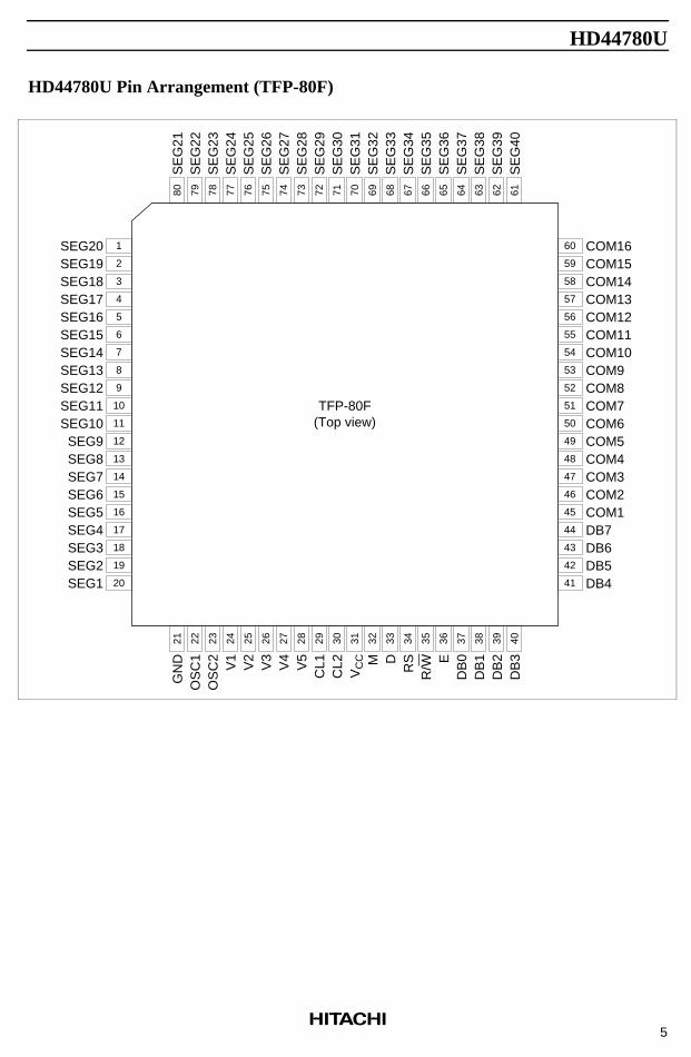
HD44780U Pin Arrangement (TFP-80F)
1
2
3
4
5
6
7
8
9
10
11
12
13
14
15
16
17
18
19
20
80 79 78 77 76 75 74 73 72 71 70 69 68 67 66 65 64 63 62 61
60
59
58
57
56
55
54
53
52
51
50
49
48
47
46
45
44
43
42
41
21 22 23 24 25 26 27 28 29 30 31 32 33 34 35 36 37 38 39 40
TFP-80F(Top view)
COM16COM15COM14COM13COM12COM11COM10COM9COM8COM7COM6COM5COM4COM3COM2COM1DB7DB6DB5DB4
SEG20SEG19SEG18SEG17SEG16SEG15SEG14SEG13SEG12SEG11SEG10SEG9SEG8SEG7SEG6SEG5SEG4SEG3SEG2SEG1
SE
G21
SE
G22
SE
G23
SE
G24
SE
G25
SE
G26
SE
G27
SE
G28
SE
G29
SE
G30
SE
G31
SE
G32
SE
G33
SE
G34
SE
G35
SE
G36
SE
G37
SE
G38
SE
G39
SE
G40
GN
DO
SC
1O
SC
2V
1V
2V
3V
4V
5C
L1C
L2V
CC M D
RS
R/W E
DB
0D
B1
DB
2D
B3
5

HD44780U
HD44780U Pad Arrangement
HD44780U
Type code
23
X
Y
42
2 1 80 63
Chip size:
Coordinate:
Origin:
Pad size:
4.90 × 4.90 mm2
Pad center (µm)
Chip center
114 × 114 µm2
6
HD44780U
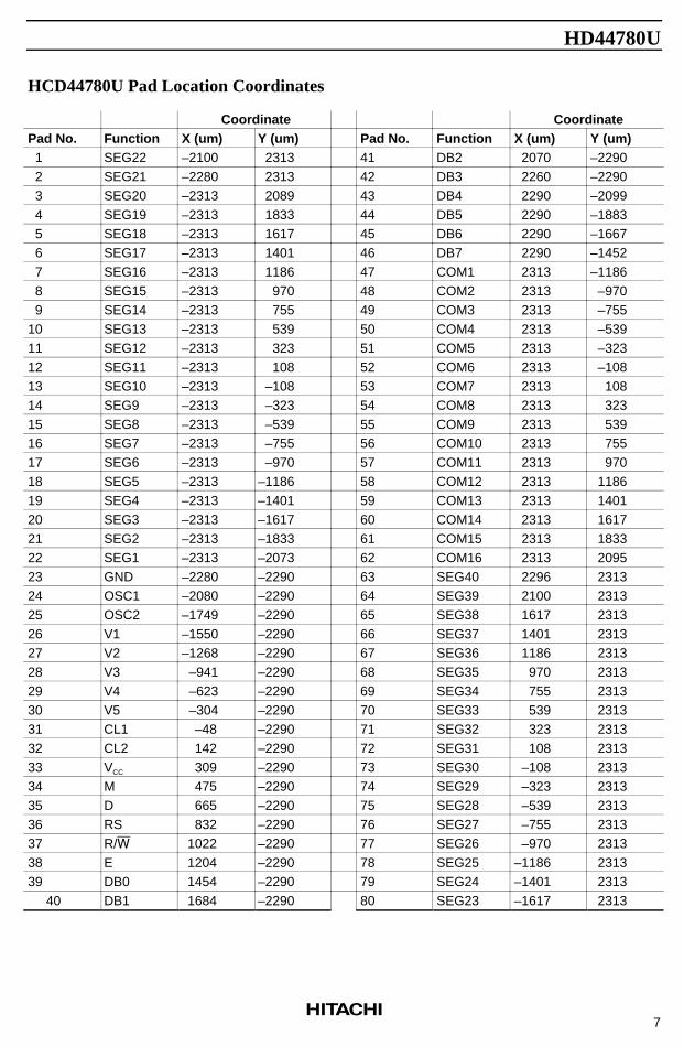
HCD44780U Pad Location Coordinates
Coordinate CoordinatePad No. Function X (um) Y (um) Pad No. Function X (um) Y (um)1 SEG22 –2100 2313 41 DB2 2070 –22902 SEG21 –2280 2313 42 DB3 2260 –22903 SEG20 –2313 2089 43 DB4 2290 –20994 SEG19 –2313 1833 44 DB5 2290 –18835 SEG18 –2313 1617 45 DB6 2290 –16676 SEG17 –2313 1401 46 DB7 2290 –14527 SEG16 –2313 1186 47 COM1 2313 –11868 SEG15 –2313 970 48 COM2 2313 –9709 SEG14 –2313 755 49 COM3 2313 –755
10 SEG13 –2313 539 50 COM4 2313 –53911 SEG12 –2313 323 51 COM5 2313 –32312 SEG11 –2313 108 52 COM6 2313 –10813 SEG10 –2313 –108 53 COM7 2313 10814 SEG9 –2313 –323 54 COM8 2313 32315 SEG8 –2313 –539 55 COM9 2313 53916 SEG7 –2313 –755 56 COM10 2313 75517 SEG6 –2313 –970 57 COM11 2313 97018 SEG5 –2313 –1186 58 COM12 2313 118619 SEG4 –2313 –1401 59 COM13 2313 140120 SEG3 –2313 –1617 60 COM14 2313 161721 SEG2 –2313 –1833 61 COM15 2313 183322 SEG1 –2313 –2073 62 COM16 2313 209523 GND –2280 –2290 63 SEG40 2296 231324 OSC1 –2080 –2290 64 SEG39 2100 231325 OSC2 –1749 –2290 65 SEG38 1617 231326 V1 –1550 –2290 66 SEG37 1401 231327 V2 –1268 –2290 67 SEG36 1186 231328 V3 –941 –2290 68 SEG35 970 231329 V4 –623 –2290 69 SEG34 755 231330 V5 –304 –2290 70 SEG33 539 231331 CL1 –48 –2290 71 SEG32 323 231332 CL2 142 –2290 72 SEG31 108 231333 VCC 309 –2290 73 SEG30 –108 231334 M 475 –2290 74 SEG29 –323 231335 D 665 –2290 75 SEG28 –539 231336 RS 832 –2290 76 SEG27 –755 231337 R/W 1022 –2290 77 SEG26 –970 231338 E 1204 –2290 78 SEG25 –1186 231339 DB0 1454 –2290 79 SEG24 –1401 2313 40 DB1 1684 –2290 80 SEG23 –1617 2313
7

HD44780U
Pin Functions
SignalNo. ofLines I/O
DeviceInterfaced with Function
RS 1 I MPU Selects registers.0: Instruction register (for write) Busy flag:
address counter (for read)1: Data register (for write and read)
R/W 1 I MPU Selects read or write.0: Write1: Read
E 1 I MPU Starts data read/write.
DB4 to DB7 4 I/O MPU Four high order bidirectional tristate data buspins. Used for data transfer and receive betweenthe MPU and the HD44780U. DB7 can be usedas a busy flag.
DB0 to DB3 4 I/O MPU Four low order bidirectional tristate data bus pins.Used for data transfer and receive between theMPU and the HD44780U.These pins are not used during 4-bit operation.
CL1 1 O Extension driver Clock to latch serial data D sent to the extensiondriver
CL2 1 O Extension driver Clock to shift serial data D
M 1 O Extension driver Switch signal for converting the liquid crystaldrive waveform to AC
D 1 O Extension driver Character pattern data corresponding to eachsegment signal
COM1 to COM16 16 O LCD Common signals that are not used are changedto non-selection waveforms. COM9 to COM16are non-selection waveforms at 1/8 duty factorand COM12 to COM16 are non-selectionwaveforms at 1/11 duty factor.
SEG1 to SEG40 40 O LCD Segment signals
V1 to V5 5 — Power supply Power supply for LCD driveVCC –V5 = 11 V (max)
VCC, GND 2 — Power supply VCC: 2.7V to 5.5V, GND: 0V
OSC1, OSC2 2 — Oscillationresistor clock
When crystal oscillation is performed, a resistormust be connected externally. When the pin inputis an external clock, it must be input to OSC1.
8

HD44780U
Function Description
Registers
The HD44780U has two 8-bit registers, an instruction register (IR) and a data register (DR).
The IR stores instruction codes, such as display clear and cursor shift, and address information for displaydata RAM (DDRAM) and character generator RAM (CGRAM). The IR can only be written from the MPU.
The DR temporarily stores data to be written into DDRAM or CGRAM and temporarily stores data to beread from DDRAM or CGRAM. Data written into the DR from the MPU is automatically written intoDDRAM or CGRAM by an internal operation. The DR is also used for data storage when reading datafrom DDRAM or CGRAM. When address information is written into the IR, data is read and then storedinto the DR from DDRAM or CGRAM by an internal operation. Data transfer between the MPU is thencompleted when the MPU reads the DR. After the read, data in DDRAM or CGRAM at the next address issent to the DR for the next read from the MPU. By the register selector (RS) signal, these two registers canbe selected (Table 1).
Busy Flag (BF)
When the busy flag is 1, the HD44780U is in the internal operation mode, and the next instruction will notbe accepted. When RS = 0 and R/W = 1 (Table 1), the busy flag is output to DB7. The next instructionmust be written after ensuring that the busy flag is 0.
Address Counter (AC)
The address counter (AC) assigns addresses to both DDRAM and CGRAM. When an address of aninstruction is written into the IR, the address information is sent from the IR to the AC. Selection of eitherDDRAM or CGRAM is also determined concurrently by the instruction.
After writing into (reading from) DDRAM or CGRAM, the AC is automatically incremented by 1(decremented by 1). The AC contents are then output to DB0 to DB6 when RS = 0 and R/W = 1 (Table 1).
Table 1 Register Selection
RS R/W Operation
0 0 IR write as an internal operation (display clear, etc.)
0 1 Read busy flag (DB7) and address counter (DB0 to DB6)
1 0 DR write as an internal operation (DR to DDRAM or CGRAM)
1 1 DR read as an internal operation (DDRAM or CGRAM to DR)
9
HD44780U
Display Data RAM (DDRAM)
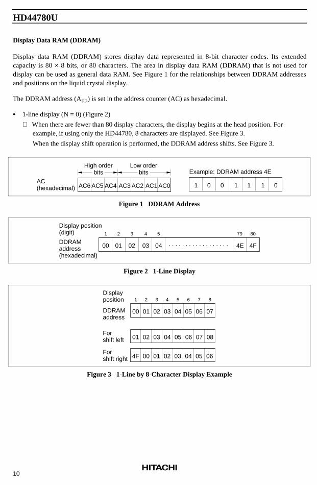
Display data RAM (DDRAM) stores display data represented in 8-bit character codes. Its extendedcapacity is 80 × 8 bits, or 80 characters. The area in display data RAM (DDRAM) that is not used fordisplay can be used as general data RAM. See Figure 1 for the relationships between DDRAM addressesand positions on the liquid crystal display.
The DDRAM address (ADD) is set in the address counter (AC) as hexadecimal.
• 1-line display (N = 0) (Figure 2)
When there are fewer than 80 display characters, the display begins at the head position. Forexample, if using only the HD44780, 8 characters are displayed. See Figure 3.
When the display shift operation is performed, the DDRAM address shifts. See Figure 3.
AC6 AC5 AC4 AC3 AC2 AC1 AC0 1 0 0 1 1 1 0AC(hexadecimal)
Example: DDRAM address 4EHigh order
bitsLow order
bits
Figure 1 DDRAM Address
00 01 02 03 04 4E 4FDDRAMaddress(hexadecimal)
Display position(digit) 1 2 3 4 5 79 80
. . . . . . . . . . . . . . . . . .
Figure 2 1-Line Display
DDRAMaddress
Displayposition 1 2 3 4 5 6 7 8
00 01 02 03 04 05 06 07
Forshift left
Forshift right 00 01 02 03 04 05 06
01 02 03 04 05 06 07 08
4F
Figure 3 1-Line by 8-Character Display Example
10
HD44780U
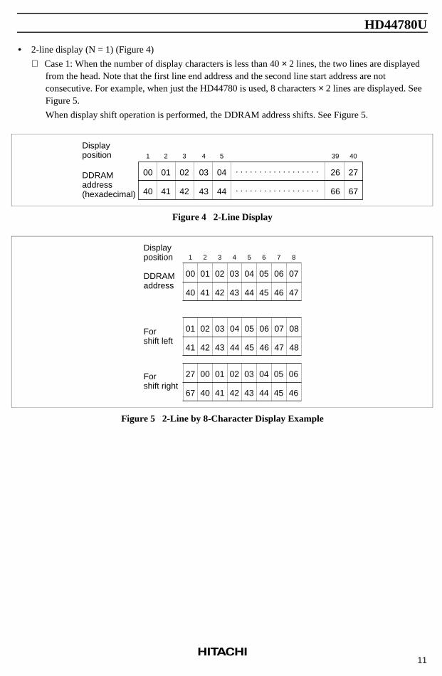
• 2-line display (N = 1) (Figure 4)
Case 1: When the number of display characters is less than 40 × 2 lines, the two lines are displayedfrom the head. Note that the first line end address and the second line start address are notconsecutive. For example, when just the HD44780 is used, 8 characters × 2 lines are displayed. SeeFigure 5.
When display shift operation is performed, the DDRAM address shifts. See Figure 5.
00 01 02 03 04 26 27DDRAMaddress(hexadecimal)
Displayposition 1 2 3 4 5 39 40
. . . . . . . . . . . . . . . . . .
40 41 42 43 44 66 67. . . . . . . . . . . . . . . . . .
Figure 4 2-Line Display
DDRAMaddress
Displayposition 1 2 3 4 5 6 7 8
00 01 02 03 04 05 06 07
Forshift left
Forshift right
40 41 42 43 44 45 46 47
01 02 03 04 05 06 07 08
41 42 43 44 45 46 47 48
00 01 02 03 04 05 06
40 41 42 43 44 45 46
27
67
Figure 5 2-Line by 8-Character Display Example
11

HD44780U
Case 2: For a 16-character × 2-line display, the HD44780 can be extended using one 40-outputextension driver. See Figure 6.
When display shift operation is performed, the DDRAM address shifts. See Figure 6.
DDRAMaddress
Displayposition 1 2 3 4 5 6 7 8 9 10 11 12 13 14 15 16
00 01 02 03 04 05 06 07 08 09 0A 0B0C0D 0E 0F
Forshift left
00 01 02 03 04 05 06 07 08 09 0A 0B0C0D 0E27
40 41 42 43 44 45 46 47 48 49 4A 4B4C4D 4E 4F
HD44780U display Extension driverdisplay
0201 03 04 05 06 07 08 09 0A 0B0C0D 0E 0F10
Forshift right
41 42 43 44 45 46 47 48 49 4A 4B4C4D 4E 4F 50
40 41 42 43 44 45 46 47 48 49 4A 4B4C4D 4E67
Figure 6 2-Line by 16-Character Display Example
12

HD44780U
Character Generator ROM (CGROM)
The character generator ROM generates 5 × 8 dot or 5 × 10 dot character patterns from 8-bit charactercodes (Table 4). It can generate 208 5 × 8 dot character patterns and 32 5 × 10 dot character patterns. User-defined character patterns are also available by mask-programmed ROM.
Character Generator RAM (CGRAM)
In the character generator RAM, the user can rewrite character patterns by program. For 5 × 8 dots, eightcharacter patterns can be written, and for 5 × 10 dots, four character patterns can be written.
Write into DDRAM the character codes at the addresses shown as the left column of Table 4 to show thecharacter patterns stored in CGRAM.
See Table 5 for the relationship between CGRAM addresses and data and display patterns.
Areas that are not used for display can be used as general data RAM.
Modifying Character Patterns
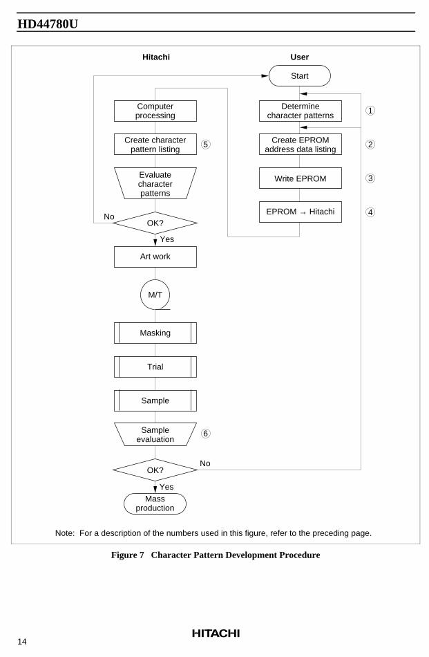
• Character pattern development procedure
The following operations correspond to the numbers listed in Figure 7:
1. Determine the correspondence between character codes and character patterns.
2. Create a listing indicating the correspondence between EPROM addresses and data.
3. Program the character patterns into the EPROM.
4. Send the EPROM to Hitachi.
5. Computer processing on the EPROM is performed at Hitachi to create a character pattern listing, whichis sent to the user.
6. If there are no problems within the character pattern listing, a trial LSI is created at Hitachi and samplesare sent to the user for evaluation. When it is confirmed by the user that the character patterns are
13
correctly written, mass production of the LSI proceeds at Hitachi.
HD44780U
Determinecharacter patterns
Create EPROMaddress data listing
Write EPROM
EPROM → Hitachi
Computerprocessing
Create characterpattern listing
Evaluatecharacterpatterns
OK?
Art work
Sampleevaluation
OK?
Masking
Trial
Sample
No
Yes
No
Yes
M/T
1
3
2
4
5
6
Note: For a description of the numbers used in this figure, refer to the preceding page.
UserHitachi
Massproduction
Start
14
Figure 7 Character Pattern Development Procedure

HD44780U
• Programming character patterns
This section explains the correspondence between addresses and data used to program character patternsin EPROM. The HD44780U character generator ROM can generate 208 5 × 8 dot character patterns and32 5 × 10 dot character patterns for a total of 240 different character patterns.
Character patterns
EPROM address data and character pattern data correspond with each other to form a 5 × 8 or 5 ×10 dot character pattern (Tables 2 and 3).
Table 2 Example of Correspondence between EPROM Address Data and Character Pattern(5 × 8 Dots)
Data
O4 O3 O2 O1 O0
0 0 0 1
0 0 1 0
0 0 1 1
0 1 0 0
0 1 1 0 0 0 1 0
EPROM Address
Character code Lineposition
LSB
0 1 0 1
0 1 1 0
0 1 1 1
0 0 0 0
1 0 0 1
1 0 1 0
1 0 1 1
1 1 0 0
1 1 0 1
1 1 1 0
1 1 1 1
1 0 0 0
1 1 0 0 1
1 0 0 0 1
1 0 0 0 1
1 0 0 0 0
1 0 0 0 0
1 0 1 1 0
Cursor position
1 1 1 1 0
0 0 0 0 0
0 0 0 0 0
0 0 0 0 0
0 0 0 0 0
0 0 0 0 0
0 0 0 0 0
0 0 0 0 0
0 0 0 0 0
0 0 0 0 0
A10 A9 A8 A7 A6 A5 A4 A3 A2 A1 A0A11
Notes: 1. EPROM addresses A11 to A4 correspond to a character code.2. EPROM addresses A3 to A0 specify a line position of the character pattern.3. EPROM data O4 to O0 correspond to character pattern data.4. EPROM data O5 to O7 must be specified as 0.5. A lit display position (black) corresponds to a 1.6. Line 9 and the following lines must be blanked with 0s for a 5 × 8 dot character fonts.
15

HD44780U
Handling unused character patterns
1. EPROM data outside the character pattern area: Always input 0s.
2. EPROM data in CGRAM area: Always input 0s. (Input 0s to EPROM addresses 00H to FFH.)
3. EPROM data used when the user does not use any HD44780U character pattern: According to the userapplication, handled in one of the two ways listed as follows.
a. When unused character patterns are not programmed: If an unused character code is written intoDDRAM, all its dots are lit. By not programing a character pattern, all of its bits become lit. (This isdue to the EPROM being filled with 1s after it is erased.)
b. When unused character patterns are programmed as 0s: Nothing is displayed even if unusedcharacter codes are written into DDRAM. (This is equivalent to a space.)
Table 3 Example of Correspondence between EPROM Address Data and Character Pattern(5 × 10 Dots)
A10 A9 A8 A7 A6 A5 A4 A3 A2 A1 A0
Data
O4 O3 O2 O1 O0
0 0 0 1
0 0 1 0
0 0 1 1
0 1 0 0
0 1 0 1 0 0 1 0
EPROM Address
Character code Lineposition
LSB
0 1 0 1
0 1 1 0
0 1 1 1
0 0 0 0 0
0 0 0 0 0
0 1 1 0 1
1 0 0 1 1
1 0 0 0 1
1 0 0 0 1
0 0 0 0
A11
1 0 0 1
1 0 1 0
1 0 1 1
1 1 0 0
1 1 0 1
1 1 1 0
1 1 1 1
1 0 0 0
Cursor position0 0 0 0 0
0 0 0 0 0
0 0 0 0 0
0 0 0 0 0
0 0 0 0 0
0 0 0 0 0
0 0 0 0 1
0 0 0 0 1
0 0 0 0 1
0 1 1 1 1
Notes: 1. EPROM addresses A11 to A3 correspond to a character code.2. EPROM addresses A3 to A0 specify a line position of the character pattern.3. EPROM data O4 to O0 correspond to character pattern data.4. EPROM data O5 to O7 must be specified as 0.5. A lit display position (black) corresponds to a 1.
16
6. Line 11 and the following lines must be blanked with 0s for a 5 × 10 dot character fonts.
HD44780U
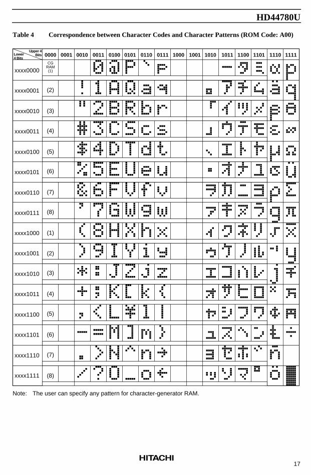
Table 4 Correspondence between Character Codes and Character Patterns (ROM Code: A00)
xxxx0000
xxxx0001
xxxx0010
xxxx0011
xxxx0100
xxxx0101
xxxx0110
xxxx0111
xxxx1000
xxxx1001
xxxx1010
xxxx1011
xxxx1100
xxxx1101
xxxx1110
xxxx1111
0000 0010 0011 0100 0101 0110 0111 1010 1011 1100 1101 1110 1111Upper 4
BitsLower 4 Bits
CGRAM(1)
(2)
(3)
(4)
(5)
(6)
(7)
(8)
(1)
(2)
(3)
(4)
(5)
(6)
(7)
(8)
0001 1000 1001
Note: The user can specify any pattern for character-generator RAM.
17
HD44780U
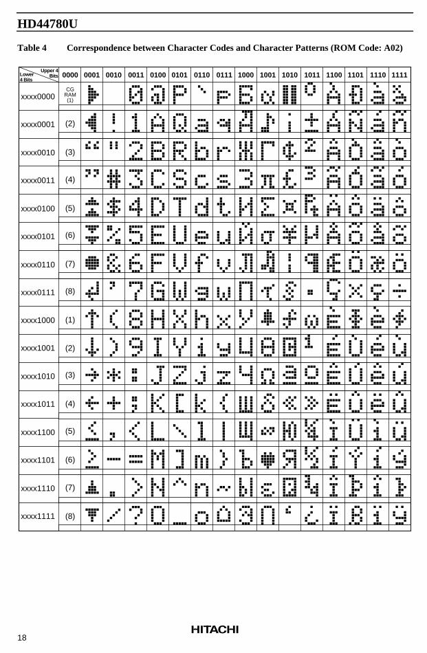
Table 4 Correspondence between Character Codes and Character Patterns (ROM Code: A02)
xxxx0000
xxxx0001
xxxx0010
xxxx0011
xxxx0100
xxxx0101
xxxx0110
xxxx0111
xxxx1000
xxxx1001
xxxx1010
xxxx1011
xxxx1100
xxxx1101
xxxx1110
xxxx1111
0000 0010 0011 0100 0101 0110 0111 1010 1011 1100 1101 1110 1111Upper 4
BitsLower 4 Bits
CGRAM(1)
(2)
(3)
(4)
(5)
(6)
(7)
(8)
(1)
(2)
(3)
(4)
(5)
(6)
(7)
(8)
0001 1000 1001
18
HD44780U
Table 5 Relationship between CGRAM Addresses, Character Codes (DDRAM) and CharacterPatterns (CGRAM Data)
Character Codes(DDRAM data) CGRAM Address
Character Patterns(CGRAM data)
7 6 5 4 3 2 1 0
0 0 0 0 * 0 0 0
0 0 0 0 * 0 0 1
0 0 0 0 * 1 1 1
5 4 3 2 1 0
0 0 0
0 0 1
1 1 1
7 6 5 4 3 2 1 0
0
0
0
0
1
1
1
1
0
0
0
0
1
1
1
1
0
0
1
1
1
1
0
0
1
1
0
0
1
1
0
0
1
1
0
0
1
1
0
0
0
0
1
1
0
1
0
1
0
1
0
1
0
1
0
1
0
1
0
1
0
1
0
1
0
1
*
*
*
*
*
*
*
*
*
*
*
*
*
*
*
*
*
*
High Low High Low High Low
Characterpattern (1)
Cursor position
1
1
1
1
1
1
1
0
1
0
1
0
1
0
0
0
0
1
1
0
0
0
1
0
1
0
1
0
1
0
0
0
1
0
0
1
0
0
0
0
0
1
1
0
1
0
0
0
1
0
0
1
1
0
0
0
0
0
1
1
1
1
1
0
1
0
0
1
0
1
0
0
0
1
1
0
1
0
0
0
Characterpattern (2)
Cursor position
For 5 × 8 dot character patterns
Notes: 1. Character code bits 0 to 2 correspond to CGRAM address bits 3 to 5 (3 bits: 8 types).2. CGRAM address bits 0 to 2 designate the character pattern line position. The 8th line is the
cursor position and its display is formed by a logical OR with the cursor.Maintain the 8th line data, corresponding to the cursor display position, at 0 as the cursor display.If the 8th line data is 1, 1 bits will light up the 8th line regardless of the cursor presence.
3. Character pattern row positions correspond to CGRAM data bits 0 to 4 (bit 4 being at the left).4. As shown Table 5, CGRAM character patterns are selected when character code bits 4 to 7 are
all 0. However, since character code bit 3 has no effect, the R display example above can beselected by either character code 00H or 08H.
5. 1 for CGRAM data corresponds to display selection and 0 to non-selection.* Indicates no effect.
19

HD44780U
Table 5 Relationship between CGRAM Addresses, Character Codes (DDRAM) and CharacterPatterns (CGRAM Data) (cont)
Character Codes(DDRAM data) CGRAM Address
Character Patterns(CGRAM data)
7 6 5 4 3 2 1 0
0 0 0 0 * 0 0
0 0 0 0 1 1
5 4 3 2 1 0
0 0
1 1
7 6 5 4 3 2 1 0
*
*
*
*
*
*
*
*
*
*
*
*
*
*
*
*
*
*
*
*
*
*
*
*
High Low High Low High Low
Characterpattern
Cursor position
0
0
0
0
1
1
1
1
0
0
0
0
1
1
1
1
0
0
0
0
0
1
1
1
1
0
0
1
1
0
0
1
1
0
0
1
1
0
0
1
1
0
0
0
1
1
0
0
1
1
0
1
0
1
0
1
0
1
0
1
0
1
0
1
0
1
0
1
1
0
1
0
1
0
1
0
0
0
0
0
0
0
0
1
1
1
1
1
1
1
1
0
0
1
1
1
1
1
1
1
*
*
*
*
*
* *
0
0
1
1
1
1
1
1
1
1
0
0
0
0
1
0
0
1
0
0
0
0
0
0
1
0
0
0
1
0
0
0
0
0
0
1
0
0
0
1
0
0
0
0
0
0
0
1
1
1
0
0
0
0
0
*
*
*
*
*
*
*
*
*
*
*
*
*
*
*
*
For 5 × 10 dot character patterns
Notes: 1. Character code bits 1 and 2 correspond to CGRAM address bits 4 and 5 (2 bits: 4 types).2. CGRAM address bits 0 to 3 designate the character pattern line position. The 11th line is the
cursor position and its display is formed by a logical OR with the cursor.Maintain the 11th line data corresponding to the cursor display positon at 0 as the cursor display.If the 11th line data is “1”, “1” bits will light up the 11th line regardless of the cursor presence.Since lines 12 to 16 are not used for display, they can be used for general data RAM.
3. Character pattern row positions are the same as 5 × 8 dot character pattern positions.4. CGRAM character patterns are selected when character code bits 4 to 7 are all 0.
However, since character code bits 0 and 3 have no effect, the P display example above can beselected by character codes 00H, 01H, 08H, and 09H.
5. 1 for CGRAM data corresponds to display selection and 0 to non-selection.* Indicates no effect.
20

HD44780U
Timing Generation Circuit
The timing generation circuit generates timing signals for the operation of internal circuits such asDDRAM, CGROM and CGRAM. RAM read timing for display and internal operation timing by MPUaccess are generated separately to avoid interfering with each other. Therefore, when writing data toDDRAM, for example, there will be no undesirable interferences, such as flickering, in areas other than thedisplay area.
Liquid Crystal Display Driver Circuit
The liquid crystal display driver circuit consists of 16 common signal drivers and 40 segment signaldrivers. When the character font and number of lines are selected by a program, the required commonsignal drivers automatically output drive waveforms, while the other common signal drivers continue tooutput non-selection waveforms.
Sending serial data always starts at the display data character pattern corresponding to the last address ofthe display data RAM (DDRAM).
Since serial data is latched when the display data character pattern corresponding to the starting addressenters the internal shift register, the HD44780U drives from the head display.
Cursor/Blink Control Circuit
The cursor/blink control circuit generates the cursor or character blinking. The cursor or the blinking willappear with the digit located at the display data RAM (DDRAM) address set in the address counter (AC).
For example (Figure 8), when the address counter is 08H, the cursor position is displayed at DDRAMaddress 08H.
AC6
0
AC5
0
AC4
0
AC3
1
AC2
0
AC1
0
AC0
0
1
00
2
01
3
02
4
03
5
04
6
05
7
06
8
07
9
08
10
09
11
0A
1
00
40
2
01
41
3
02
42
4
03
43
5
04
44
6
05
45
7
06
46
8
07
47
9
08
48
10
09
49
11
0A
4A
AC
cursor position
cursor position
Display position
DDRAM address(hexadecimal)
Display position
DDRAM address(hexadecimal)
For a 1-line display
For a 2-line display
Note: The cursor or blinking appears when the address counter (AC) selects the character generator RAM (CGRAM). However, the cursor and blinking become meaningless.The cursor or blinking is displayed in the meaningless position when the AC is a CGRAM address.
21
Figure 8 Cursor/Blink Display Example
HD44780U
Interfacing to the MPU
The HD44780U can send data in either two 4-bit operations or one 8-bit operation, thus allowinginterfacing with 4- or 8-bit MPUs.
• For 4-bit interface data, only four bus lines (DB4 to DB7) are used for transfer. Bus lines DB0 to DB3are disabled. The data transfer between the HD44780U and the MPU is completed after the 4-bit datahas been transferred twice. As for the order of data transfer, the four high order bits (for 8-bit operation,DB4 to DB7) are transferred before the four low order bits (for 8-bit operation, DB0 to DB3).
The busy flag must be checked (one instruction) after the 4-bit data has been transferred twice. Twomore 4-bit operations then transfer the busy flag and address counter data.
• For 8-bit interface data, all eight bus lines (DB0 to DB7) are used.
RS
R/W
E
IR7
IR6
IR5
IR4
BF
AC6
AC5
AC4
DB7
DB6
DB5
DB4
Instruction register (IR)write
Busy flag (BF) andaddress counter (AC)read
Data register (DR)read
IR3
IR2
IR1
IR0
AC3
AC2
AC1
AC0
DR7
DR6
DR5
DR4
DR3
DR2
DR1
DR0
Figure 9 4-Bit Transfer Example
22

HD44780U
Reset Function
Initializing by Internal Reset Circuit
An internal reset circuit automatically initializes the HD44780U when the power is turned on. Thefollowing instructions are executed during the initialization. The busy flag (BF) is kept in the busy stateuntil the initialization ends (BF = 1). The busy state lasts for 10 ms after VCC rises to 4.5 V.
1. Display clear
2. Function set:
DL = 1; 8-bit interface data
N = 0; 1-line display
F = 0; 5 × 8 dot character font
3. Display on/off control:
D = 0; Display off
C = 0; Cursor off
B = 0; Blinking off
4. Entry mode set:
I/D = 1; Increment by 1
S = 0; No shift
Note: If the electrical characteristics conditions listed under the table Power Supply Conditions UsingInternal Reset Circuit are not met, the internal reset circuit will not operate normally and will fail toinitialize the HD44780U. For such a case, initial-ization must be performed by the MPU asexplained in the section, Initializing by Instruction.
Instructions
Outline
Only the instruction register (IR) and the data register (DR) of the HD44780U can be controlled by theMPU. Before starting the internal operation of the HD44780U, control information is temporarily storedinto these registers to allow interfacing with various MPUs, which operate at different speeds, or variousperipheral control devices. The internal operation of the HD44780U is determined by signals sent from theMPU. These signals, which include register selection signal (RS), read/
write signal (R/W), and the data bus (DB0 to DB7), make up the HD44780U instructions (Table 6). Thereare four categories of instructions that:
• Designate HD44780U functions, such as display format, data length, etc.
• Set internal RAM addresses
• Perform data transfer with internal RAM
• Perform miscellaneous functions
23

HD44780U
Normally, instructions that perform data transfer with internal RAM are used the most. However, auto-incrementation by 1 (or auto-decrementation by 1) of internal HD44780U RAM addresses after each datawrite can lighten the program load of the MPU. Since the display shift instruction (Table 11) can performconcurrently with display data write, the user can minimize system development time with maximumprogramming efficiency.
When an instruction is being executed for internal operation, no instruction other than the busy flag/addressread instruction can be executed.
Because the busy flag is set to 1 while an instruction is being executed, check it to make sure it is 0 beforesending another instruction from the MPU.
Note: Be sure the HD44780U is not in the busy state (BF = 0) before sending an instruction from theMPU to the HD44780U. If an instruction is sent without checking the busy flag, the time betweenthe first instruction and next instruction will take much longer than the instruction time itself. Referto Table 6 for the list of each instruc-tion execution time.
Table 6 Instructions
Code Execution Time(max) (when fcp or
Instruction RS R/W DB7 DB6 DB5 DB4 DB3 DB2 DB1 DB0 Description fOSC is 270 kHz)
Cleardisplay
0 0 0 0 0 0 0 0 0 1 Clears entire display andsets DDRAM address 0 inaddress counter.
Returnhome
0 0 0 0 0 0 0 0 1 — Sets DDRAM address 0 inaddress counter. Alsoreturns display from beingshifted to original position.DDRAM contents remainunchanged.
1.52 ms
Entrymode set
0 0 0 0 0 0 0 1 I/D S Sets cursor move directionand specifies display shift.These operations areperformed during data writeand read.
37 µs
Displayon/offcontrol
0 0 0 0 0 0 1 D C B Sets entire display (D) on/off,cursor on/off (C), andblinking of cursor positioncharacter (B).
37 µs
Cursor ordisplayshift
0 0 0 0 0 1 S/C R/L — — Moves cursor and shiftsdisplay without changingDDRAM contents.
37 µs
Functionset
0 0 0 0 1 DL N F — — Sets interface data length(DL), number of display lines(N), and character font (F).
37 µs
SetCGRAMaddress
0 0 0 1 ACG ACG ACG ACG ACG ACG Sets CGRAM address.CGRAM data is sent andreceived after this setting.
37 µs
SetDDRAMaddress
0 0 1 ADD ADD ADD ADD ADD ADD ADD Sets DDRAM address.DDRAM data is sent andreceived after this setting.
37 µs
Read busyflag &address
0 1 BF AC AC AC AC AC AC AC Reads busy flag (BF)indicating internal operationis being performed andreads address countercontents.
0 µs
24

HD44780U
Table 6 Instructions (cont)
CodeExecution Time(max) (when fcp or
Instruction RS R/W DB7 DB6 DB5 DB4 DB3 DB2 DB1 DB0 Description fOSC is 270 kHz)
Write datato CG orDDRAM
1 0 Write data Writes data into DDRAM orCGRAM.
37 µstADD = 4 µs*
Read datafrom CG orDDRAM
1 1 Read data Reads data from DDRAM orCGRAM.
37 µstADD = 4 µs*
I/D = 1: IncrementI/D = 0: DecrementS = 1: Accompanies display shiftS/C = 1: Display shiftS/C = 0: Cursor moveR/L = 1: Shift to the rightR/L = 0: Shift to the leftDL = 1: 8 bits, DL = 0: 4 bitsN = 1: 2 lines, N = 0: 1 lineF = 1: 5 × 10 dots, F = 0: 5 × 8 dotsBF = 1: Internally operatingBF = 0: Instructions acceptable
DDRAM: Display data RAMCGRAM: Character generator
RAMACG: CGRAM addressADD: DDRAM address
(corresponds to cursoraddress)
AC: Address counter used forboth DD and CGRAMaddresses
Execution timechanges whenfrequency changesExample:When fcp or fOSC is250 kHz,
37 µs × = 40 µs270 250
Note: — indicates no effect.* After execution of the CGRAM/DDRAM data write or read instruction, the RAM address counter
is incremented or decremented by 1. The RAM address counter is updated after the busy flagturns off. In Figure 10, tADD is the time elapsed after the busy flag turns off until the addresscounter is updated.
Busy stateBusy signal(DB7 pin)
Address counter(DB0 to DB6 pins)
t ADD
A A + 1
Note: t depends on the operation frequencyt = 1.5/(f or f ) seconds
ADD
ADD cp OSC
Figure 10 Address Counter Update
25

HD44780U
Instruction Description
Clear Display
Clear display writes space code 20H (character pattern for character code 20H must be a blank pattern) intoall DDRAM addresses. It then sets DDRAM address 0 into the address counter, and returns the display toits original status if it was shifted. In other words, the display disappears and the cursor or blinking goes tothe left edge of the display (in the first line if 2 lines are displayed). It also sets I/D to 1 (increment mode)in entry mode. S of entry mode does not change.
Return Home
Return home sets DDRAM address 0 into the address counter, and returns the display to its original statusif it was shifted. The DDRAM contents do not change.
The cursor or blinking go to the left edge of the display (in the first line if 2 lines are displayed).
Entry Mode Set
I/D: Increments (I/D = 1) or decrements (I/D = 0) the DDRAM address by 1 when a character code iswritten into or read from DDRAM.
The cursor or blinking moves to the right when incremented by 1 and to the left when decremented by 1.The same applies to writing and reading of CGRAM.
S: Shifts the entire display either to the right (I/D = 0) or to the left (I/D = 1) when S is 1. The display doesnot shift if S is 0.
If S is 1, it will seem as if the cursor does not move but the display does. The display does not shift whenreading from DDRAM. Also, writing into or reading out from CGRAM does not shift the display.
Display On/Off Control
D: The display is on when D is 1 and off when D is 0. When off, the display data remains in DDRAM, butcan be displayed instantly by setting D to 1.
C: The cursor is displayed when C is 1 and not displayed when C is 0. Even if the cursor disappears, thefunction of I/D or other specifications will not change during display data write. The cursor is displayedusing 5 dots in the 8th line for 5 × 8 dot character font selection and in the 11th line for the 5 × 10 dotcharacter font selection (Figure 13).
B: The character indicated by the cursor blinks when B is 1 (Figure 13). The blinking is displayed asswitching between all blank dots and displayed characters at a speed of 409.6-ms intervals when fcp or fOSC
is 250 kHz. The cursor and blinking can be set to display simultaneously. (The blinking frequency changesaccording to fOSC or the reciprocal of fcp. For example, when fcp is 270 kHz, 409.6 × 250/270 = 379.2 ms.)
26
HD44780U
Cursor or Display Shift
Cursor or display shift shifts the cursor position or display to the right or left without writing or readingdisplay data (Table 7). This function is used to correct or search the display. In a 2-line display, the cursormoves to the second line when it passes the 40th digit of the first line. Note that the first and second linedisplays will shift at the same time.
When the displayed data is shifted repeatedly each line moves only horizontally. The second line displaydoes not shift into the first line position.
The address counter (AC) contents will not change if the only action performed is a display shift.
Function Set
DL: Sets the interface data length. Data is sent or received in 8-bit lengths (DB7 to DB0) when DL is 1,and in 4-bit lengths (DB7 to DB4) when DL is 0.When 4-bit length is selected, data must be sent orreceived twice.
N: Sets the number of display lines.
F: Sets the character font.
Note: Perform the function at the head of the program before executing any instructions (except for theread busy flag and address instruction). From this point, the function set instruction cannot beexecuted unless the interface data length is changed.
Set CGRAM Address
Set CGRAM address sets the CGRAM address binary AAAAAA into the address counter.
Data is then written to or read from the MPU for CGRAM.
27

HD44780U
Code Note: Don’t care.*
Code
Code
Code
RS
0
R/W
0
DB7
0
DB6
0
DB5
0
DB4
0
DB3
0
DB2
0
DB1
0
DB0
1
RS
0
R/W
0
DB7
0
DB6
0
DB5
0
DB4
0
DB3
0
DB2
0
DB1
1
DB0
*
RS
0
R/W
0
DB7
0
DB6
0
DB5
0
DB4
0
DB3
0
DB2
1
DB1
I/D
DB0
S
RS
0
R/W
0
DB7
0
DB6
0
DB5
0
DB4
0
DB3
1
DB2
D
DB1
C
DB0
B
Return home
Clear display
Entry mode set
Display on/off control
RS
0
R/W
0
DB7
0
DB6
0
DB5
0
DB4
1
DB3
S/CCode
DB2
R/L
DB1 DB0
Code
Code
Higherorder bit
Lowerorder bit
*Cursor ordisplay shift
Function set
Set CGRAM address
*
RS
0
R/W
0
DB7
0
DB6
0
DB5
1
DB4
DL
DB3
N
DB2
F
DB1 DB0
* *
RS
0
R/W
0
DB7
0
DB6
1
DB5
A
DB4
A
DB3
A
DB2
A
DB1 DB0
A A
Note: Don’t care.*
Figure 11 Instruction (1)
28

HD44780U
Set DDRAM Address
Set DDRAM address sets the DDRAM address binary AAAAAAA into the address counter.
Data is then written to or read from the MPU for DDRAM.
However, when N is 0 (1-line display), AAAAAAA can be 00H to 4FH. When N is 1 (2-line display),AAAAAAA can be 00H to 27H for the first line, and 40H to 67H for the second line.
Read Busy Flag and Address
Read busy flag and address reads the busy flag (BF) indicating that the system is now internally operatingon a previously received instruction. If BF is 1, the internal operation is in progress. The next instructionwill not be accepted until BF is reset to 0. Check the BF status before the next write operation. At the sametime, the value of the address counter in binary AAAAAAA is read out. This address counter is used byboth CG and DDRAM addresses, and its value is determined by the previous instruction. The addresscontents are the same as for instructions set CGRAM address and set DDRAM address.
Table 7 Shift Function
S/C R/L
0 0 Shifts the cursor position to the left. (AC is decremented by one.)
0 1 Shifts the cursor position to the right. (AC is incremented by one.)
1 0 Shifts the entire display to the left. The cursor follows the display shift.
1 1 Shifts the entire display to the right. The cursor follows the display shift.
Table 8 Function Set
N F
No. ofDisplayLines Character Font
DutyFactor Remarks
0 0 1 5 × 8 dots 1/8
0 1 1 5 × 10 dots 1/11
1 * 2 5 × 8 dots 1/16 Cannot display two lines for 5 × 10 dot character font
Note: * Indicates don’t care.
29

HD44780U
Cursor
5 8 dotcharacter font
5 10 dotcharacter font
× × Alternating display
Blink display exampleCursor display example
Figure 12 Cursor and Blinking
RS
0
R/W
0
DB7
1
DB6
A
DB5
A
DB4
A
DB3
ACode
DB2
A
DB1
A
DB0
A
Higherorder bit
Lowerorder bit
RS
0
R/W
1
DB7
BF
DB6
A
DB5
A
DB4
A
DB3
ACode
DB2
A
DB1
A
DB0
A
Higherorder bit
Lowerorder bit
Set DDRAM address
Read busy flagand address
Figure 13 Instruction (2)
30
HD44780U
Write Data to CG or DDRAM
Write data to CG or DDRAM writes 8-bit binary data DDDDDDDD to CG or DDRAM.
To write into CG or DDRAM is determined by the previous specification of the CGRAM or DDRAMaddress setting. After a write, the address is automatically incremented or decremented by 1 according tothe entry mode. The entry mode also determines the display shift.
Read Data from CG or DDRAM
Read data from CG or DDRAM reads 8-bit binary data DDDDDDDD from CG or DDRAM.
The previous designation determines whether CG or DDRAM is to be read. Before entering this readinstruction, either CGRAM or DDRAM address set instruction must be executed. If not executed, the firstread data will be invalid. When serially executing read instructions, the next address data is normally readfrom the second read. The address set instructions need not be executed just before this read instructionwhen shifting the cursor by the cursor shift instruction (when reading out DDRAM). The operation of thecursor shift instruction is the same as the set DDRAM address instruction.
After a read, the entry mode automatically increases or decreases the address by 1. However, display shiftis not executed regardless of the entry mode.
Note: The address counter (AC) is automatically incremented or decremented by 1 after the writeinstructions to CGRAM or DDRAM are executed. The RAM data selected by the AC cannot beread out at this time even if read instructions are executed. Therefore, to correctly read data,execute either the address set instruction or cursor shift instruction (only with DDRAM), then justbefore reading the desired data, execute the read instruction from the second time the readinstruction is sent.
RS
1
R/W
1
DB7
D
DB6
D
DB5
D
DB4
D
DB3
DCode
DB2
D
DB1
D
DB0
D
Higherorder bits
Lowerorder bits
RS
1
R/W
0
DB7
D
DB6
D
DB5
D
DB4
D
DB3
DCode
DB2
D
DB1
D
DB0
D
Higherorder bits
Lowerorder bits
Read data fromCG or DDRAM
Write data toCG or DDRAM
Figure 14 Instruction (3)
31

#*
HD44780U
Interfacing the HD44780U
Interface to MPUs
• Interfacing to an 8-bit MPU
See Figure 16 for an example of using a I/O port (for a single-chip microcomputer) as an interfacedevice.
In this example, P30 to P37 are connected to the data bus DB0 to DB7, and P75 to P77 are connected toE, R/W, and RS, respectively.
%&,+,
RS
R/W
E
Internaloperation
DB7
Functioning
Data Busy BusyNotbusy Data
Instructionwrite
Busy flagcheck
Busy flagcheck
Busy flagcheck
Instructionwrite
Figure 15 Example of Busy Flag Check Timing Sequence
P30 to P37
P77 P76P75
16
40
H8/325 HD44780U
8DB0 to DB7
ERSR/W
LCD
COM1 toCOM16
SEG1 toSEG40
Figure 16 H8/325 Interface (Single-Chip Mode)
32
)0

HD44780U
• Interfacing to a 4-bit MPU
The HD44780U can be connected to the I/O port of a 4-bit MPU. If the I/O port has enough bits, 8-bitdata can be transferred. Otherwise, one data transfer must be made in two operations for 4-bit data. Inthis case, the timing sequence becomes somewhat complex. (See Figure 17.)
See Figure 18 for an interface example to the HMCS4019R.
Note that two cycles are needed for the busy flag check as well as for the data transfer. The 4-bitoperation is selected by the program.
#$*'./!"()
RS
R/W
E
Internaloperation
DB7 IR7 IR3 Busy AC3Not
busy AC3 D7 D3
Instructionwrite
Busy flagcheck
Busy flagcheck
Instructionwrite
Note: IR7 , IR3 are the 7th and 3rd bits of the instruction.AC3 is the 3rd bit of the address counter.
Functioning
Figure 17 Example of 4-Bit Data Transfer Timing Sequence
D15
D14
D13
R10 to R13
RS
R/W
E
DB4 to DB7
COM1 toCOM16
SEG1 toSEG40
4 40
16
LCD
HMCS4019R HD44780
33
Figure 18 Example of Interface to HMCS4019R

HD44780U
Interface to Liquid Crystal Display
Character Font and Number of Lines: The HD44780U can perform two types of displays, 5 × 8 dot and5 × 10 dot character fonts, each with a cursor.
Up to two lines are displayed for 5 × 8 dots and one line for 5 × 10 dots. Therefore, a total of three
types of common signals are available (Table 9).
The number of lines and font types can be selected by the program. (See Table 6, Instructions.)
Connection to HD44780 and Liquid Crystal Display: See Figure 19 for the connection examples.
Table 9 Common Signals
Number of Lines Character Font Number of Common Signals Duty Factor
1 5 × 8 dots + cursor 8 1/8
1 5 × 10 dots + cursor 11 1/11
2 5 × 8 dots + cursor 16 1/16
COM1
COM8
SEG1
SEG40
COM1
COM11
SEG1
SEG40
HD44780
Example of a 5 × 8 dot, 8-character × 1-line display (1/4 bias, 1/8 duty cycle)
Example of a 5 × 10 dot, 8-character × 1-line display (1/4 bias, 1/11 duty cycle)
HD44780
Figure 19 Liquid Crystal Display and HD44780 Connections
34

HD44780U
Since five segment signal lines can display one digit, one HD44780U can display up to 8 digits for a 1-linedisplay and 16 digits for a 2-line display.
The examples in Figure 19 have unused common signal pins, which always output non-selectionwaveforms. When the liquid crystal display panel has unused extra scanning lines, connect the extrascanning lines to these common signal pins to avoid any undesirable effects due to crosstalk during thefloating state.
COM1
COM8
SEG1
SEG40
HD44780
COM9
COM16
Example of a 5 × 8 dot, 8-character × 2-line display (1/5 bias, 1/16 duty cycle)
Figure 19 Liquid Crystal Display and HD44780 Connections (cont)
35

HD44780U
Connection of Changed Matrix Layout: In the preceding examples, the number of lines correspond to thescanning lines. However, the following display examples (Figure 20) are made possible by altering thematrix layout of the liquid crystal display panel. In either case, the only change is the layout. The displaycharacteristics and the number of liquid crystal display characters depend on the number of commonsignals or on duty factor. Note that the display data RAM (DDRAM) addresses for 4 characters × 2 linesand for 16 characters × 1 line are the same as in Figure 19.
COM1
COM8
SEG1
SEG40
COM9
COM16
HD44780
5 × 8 dot, 16-character × 1-line display(1/5 bias, 1/16 duty cycle)
Figure 20 Changed Matrix Layout Displays
36

HD44780U
Power Supply for Liquid Crystal Display Drive
Various voltage levels must be applied to pins V1 to V5 of the HD44780U to obtain the liquid crystaldisplay drive waveforms. The voltages must be changed according to the duty factor (Table 10).
VLCD is the peak value for the liquid crystal display drive waveforms, and resistance dividing providesvoltages V1 to V5 (Figure 21).
Table 10 Duty Factor and Power Supply for Liquid Crystal Display Drive
Duty Factor
1/8, 1/11 1/16
Bias
Power Supply 1/4 1/5
V1 VCC–1/4 VLCD VCC–1/5 VLCD
V2 VCC–1/2 VLCD VCC–2/5 VLCD
V3 VCC–1/2 VLCD VCC–3/5 VLCD
V4 VCC–3/4 VLCD VCC–4/5 VLCD
V5 VCC–VLCD VCC–VLCD
VCC
V1
V4
V5
V2
V3
VCC
V1
V2
V3
V4
V5
R
R
R
R
VR
–5 V
VCC (+5 V)
–5 V
VCC (+5 V)
R
R
R
R
R
VR
VLCDVLCD
1/4 bias(1/8, 1/11 duty cycle)
1/5 bias(1/16, duty cycle)
37
Figure 21 Drive Voltage Supply Example

HD44780U
Relationship between Oscillation Frequency and Liquid Crystal Display FrameFrequency
The liquid crystal display frame frequencies of Figure 22 apply only when the oscillation frequency is 270kHz (one clock pulse of 3.7 µs).
1 2 3 4 8 1 2
1 2 3 4 11 1 2
1 2 3 4 16 1 2
400 clocks
400 clocks
200 clocks
1 frame
1 frame
1 frame
1/8 duty cycle
1/11 duty cycle
1/16 duty cycle
VCC
V1
V2 (V3)
V4
V5
VCC
V1
V2 (V3)
V4
V5
VCC
V1
V2
V3
V4
V5
COM1
COM1
COM1
1 frame = 3.7 µs × 400 × 8 = 11850 µs = 11.9 ms
Frame frequency = = 84.3 Hz111.9 ms
1 frame = 3.7 µs × 400 × 11 = 16300 µs = 16.3 ms
Frame frequency = = 61.4 Hz116.3 ms
1 frame = 3.7 µs × 200 × 16 = 11850 µs = 11.9 ms
Frame frequency = = 84.3 Hz111.9 ms
Figure 22 Frame Frequency
38

HD44780U
Instruction and Display Correspondence
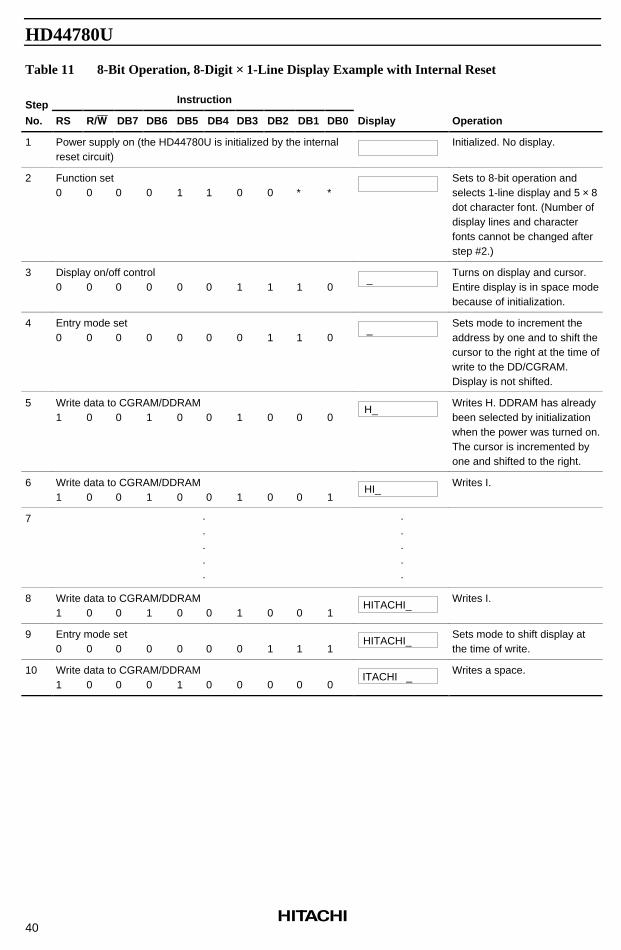
• 8-bit operation, 8-digit × 1-line display with internal reset
Refer to Table 11 for an example of an 8-digit × 1-line display in 8-bit operation. The HD44780Ufunctions must be set by the function set instruction prior to the display. Since the display data RAMcan store data for 80 characters, as explained before, the RAM can be used for displays such as foradvertising when combined with the display shift operation.
Since the display shift operation changes only the display position with DDRAM contents unchanged,the first display data entered into DDRAM can be output when the return home operation is performed.
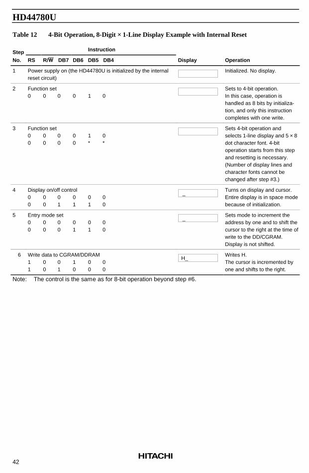
• 4-bit operation, 8-digit × 1-line display with internal reset
The program must set all functions prior to the 4-bit operation (Table 12). When the power is turned on,8-bit operation is automatically selected and the first write is performed as an 8-bit operation. SinceDB0 to DB3 are not connected, a rewrite is then required. However, since one operation is completed intwo accesses for 4-bit operation, a rewrite is needed to set the functions (see Table 12). Thus, DB4 toDB7 of the function set instruction is written twice.
• 8-bit operation, 8-digit × 2-line display
For a 2-line display, the cursor automatically moves from the first to the second line after the 40th digitof the first line has been written. Thus, if there are only 8 characters in the first line, the DDRAMaddress must be again set after the 8th character is completed. (See Table 13.) Note that the display shiftoperation is performed for the first and second lines. In the example of Table 13, the display shift isperformed when the cursor is on the second line. However, if the shift operation is performed when thecursor is on the first line, both the first and second lines move together. If the shift is repeated, thedisplay of the second line will not move to the first line. The same display will only shift within its ownline for the number of times the shift is repeated.
Note: When using the internal reset, the electrical characteristics in the Power Supply Conditions UsingInternal Reset Circuit table must be satisfied. If not, the HD44780U must be initialized by
39
instructions. See the section, Initializing by Instruction.
HD44780U
Table 11 8-Bit Operation, 8-Digit × 1-Line Display Example with Internal Reset
Step Instruction
No. RS R/W DB7 DB6 DB5 DB4 DB3 DB2 DB1 DB0 Display Operation
1 Power supply on (the HD44780U is initialized by the internalreset circuit)
Initialized. No display.
2 Function set0 0 0 0 1 1 0 0 * *
Sets to 8-bit operation andselects 1-line display and 5 × 8dot character font. (Number ofdisplay lines and characterfonts cannot be changed afterstep #2.)
3 Display on/off control0 0 0 0 0 0 1 1 1 0
_ Turns on display and cursor.Entire display is in space modebecause of initialization.
4 Entry mode set0 0 0 0 0 0 0 1 1 0
_ Sets mode to increment theaddress by one and to shift thecursor to the right at the time ofwrite to the DD/CGRAM.Display is not shifted.
5 Write data to CGRAM/DDRAM1 0 0 1 0 0 1 0 0 0
H_ Writes H. DDRAM has alreadybeen selected by initializationwhen the power was turned on.The cursor is incremented byone and shifted to the right.
6 Write data to CGRAM/DDRAM1 0 0 1 0 0 1 0 0 1
HI_ Writes I.
7 ·····
·····
8 Write data to CGRAM/DDRAM1 0 0 1 0 0 1 0 0 1
HITACHI_ Writes I.
9 Entry mode set0 0 0 0 0 0 0 1 1 1
HITACHI_ Sets mode to shift display atthe time of write.
10 Write data to CGRAM/DDRAM1 0 0 0 1 0 0 0 0 0
ITACHI _ Writes a space.
40

HD44780U
Table 11 8-Bit Operation, 8-Digit × 1-Line Display Example with Internal Reset (cont)
Step Instruction
No. RS R/W DB7 DB6 DB5 DB4 DB3 DB2 DB1 DB0 Display Operation
11 Write data to CGRAM/DDRAM1 0 0 1 0 0 1 1 0 1
TACHI M_ Writes M.
12 ·····
·····
13 Write data to CGRAM/DDRAM1 0 0 1 0 0 1 1 1 1
MICROKO_ Writes O.
14 Cursor or display shift0 0 0 0 0 1 0 0 * *
MICROKO _Shifts only the cursor positionto the left.
15 Cursor or display shift0 0 0 0 0 1 0 0 * *
MICROKO _Shifts only the cursor positionto the left.
16 Write data to CGRAM/DDRAM1 0 0 1 0 0 0 0 1 1
ICROCO _Writes C over K.The display moves to the left.
17 Cursor or display shift0 0 0 0 0 1 1 1 * *
MICROCO _Shifts the display and cursorposition to the right.
18 Cursor or display shift0 0 0 0 0 1 0 1 * *
MICROCO_ Shifts the display and cursorposition to the right.
19 Write data to CGRAM/DDRAM1 0 0 1 0 0 1 1 0 1
ICROCOM_ Writes M.
20 ·····
·····
21 Return home0 0 0 0 0 0 0 0 1 0
HITACHI _ Returns both display andcursor to the original position(address 0).
41
HD44780U
Table 12 4-Bit Operation, 8-Digit × 1-Line Display Example with Internal Reset
Step Instruction
No. RS R/W DB7 DB6 DB5 DB4 Display Operation
1 Power supply on (the HD44780U is initialized by the internalreset circuit)
Initialized. No display.
2 Function set0 0 0 0 1 0
Sets to 4-bit operation.In this case, operation ishandled as 8 bits by initializa-tion, and only this instructioncompletes with one write.
3 Function set0 0 0 0 1 00 0 0 0 * *
Sets 4-bit operation andselects 1-line display and 5 × 8dot character font. 4-bitoperation starts from this stepand resetting is necessary.(Number of display lines andcharacter fonts cannot bechanged after step #3.)
4 Display on/off control0 0 0 0 0 00 0 1 1 1 0
_ Turns on display and cursor.Entire display is in space modebecause of initialization.
5 Entry mode set0 0 0 0 0 00 0 0 1 1 0
_ Sets mode to increment theaddress by one and to shift thecursor to the right at the time ofwrite to the DD/CGRAM.Display is not shifted.
6 Write data to CGRAM/DDRAM1 0 0 1 0 01 0 1 0 0 0
H_ Writes H.The cursor is incremented byone and shifts to the right.
Note: The control is the same as for 8-bit operation beyond step #6.
42

HD44780U
Table 13 8-Bit Operation, 8-Digit × 2-Line Display Example with Internal Reset
Step Instruction
No. RS R/W DB7 DB6 DB5 DB4 DB3 DB2 DB1 DB0 Display Operation
1 Power supply on (the HD44780U is initialized by the internalreset circuit)
Initialized. No display.
2 Function set0 0 0 0 1 1 1 0 * *
Sets to 8-bit operation andselects 2-line display and 5 × 8dot character font.
3 Display on/off control0 0 0 0 0 0 1 1 1 0
_ Turns on display and cursor.All display is in space modebecause of initialization.
4 Entry mode set0 0 0 0 0 0 0 1 1 0
_ Sets mode to increment theaddress by one and to shift thecursor to the right at the time ofwrite to the DD/CGRAM.Display is not shifted.
5 Write data to CGRAM/DDRAM1 0 0 1 0 0 1 0 0 0
H_ Writes H. DDRAM has alreadybeen selected by initializationwhen the power was turned on.The cursor is incremented byone and shifted to the right.
6 ·····
·····
7 Write data to CGRAM/DDRAM1 0 0 1 0 0 1 0 0 1
HITACHI_ Writes I.
8 Set DDRAM address0 0 1 1 0 0 0 0 0 0
HITACHI _
Sets DDRAM address so thatthe cursor is positioned at thehead of the second line.
43

HD44780U
Table 13 8-Bit Operation, 8-Digit × 2-Line Display Example with Internal Reset (cont)
Step Instruction
No. RS R/W DB7 DB6 DB5 DB4 DB3 DB2 DB1 DB0 Display Operation
9 Write data to CGRAM/DDRAM1 0 0 1 0 0 1 1 0 1
HITACHI M_
Writes M.
10 ·····
·····
11 Write data to CGRAM/DDRAM1 0 0 1 0 0 1 1 1 1
HITACHI MICROCO_
Writes O.
12 Entry mode set0 0 0 0 0 0 0 1 1 1
HITACHI MICROCO_
Sets mode to shift display atthe time of write.
13 Write data to CGRAM/DDRAM1 0 0 1 0 0 1 1 0 1
ITACHI ICROCOM_
Writes M. Display is shifted tothe left. The first and secondlines both shift at the sametime.
14 ·····
·····
15 Return home0 0 0 0 0 0 0 0 1 0
HITACHI MICROCOM _
Returns both display andcursor to the original position(address 0).
44

HD44780U
Initializing by Instruction
If the power supply conditions for correctly operating the internal reset circuit are not met, initialization byinstructions becomes necessary.
Refer to Figures 23 and 24 for the procedures on 8-bit and 4-bit initializations, respectively.
Power on
Wait for more than 15 msafter VCC rises to 4.5 V
Wait for more than 4.1 ms
Wait for more than 100 µs
RS0
R/W0
DB7 0
DB6 0
DB5 1
DB4 1
DB3DB2 DB1 DB0 * * * *
RS0
R/W0
DB7 0
DB6 0
DB51
DB4 1
DB3DB2DB1DB0* * * *
RS0
R/W0
DB7 0
DB6 0
DB5 1
DB4 1
DB3DB2DB1* * *
DB0*
RS0
R/W0
DB7 0
DB6 0
DB5 1
DB4 1
DB3 N
DB2F
DB1DB0* *
0
0
0
0
0
0
0
0
0
0
0
0
0
0
0
0
0
0
1
0
0
0
0
1
0
0
I/D
0
1
S
Initialization ends
BF cannot be checked before this instruction.
Function set (Interface is 8 bits long.)
BF cannot be checked before this instruction.
Function set (Interface is 8 bits long.)
BF cannot be checked before this instruction.
Function set (Interface is 8 bits long.)
BF can be checked after the following instructions. When BF is not checked, the waiting time between instructions is longer than the execution instuction time. (See Table 6.)
Function set (Interface is 8 bits long. Specify the number of display lines and character font.)The number of display lines and character fontcannot be changed after this point.
Display off
Display clear
Entry mode set
Wait for more than 40 msafter VCC rises to 2.7 V
45
Figure 23 8-Bit Interface
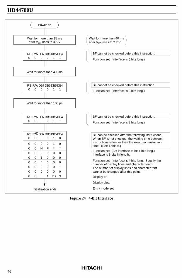
HD44780U
Initialization ends
Wait for more than 15 msafter VCC rises to 4.5 V
Wait for more than 40 msafter VCC rises to 2.7 V
BF cannot be checked before this instruction.
Function set (Interface is 8 bits long.)
BF cannot be checked before this instruction.
Function set (Interface is 8 bits long.)
BF cannot be checked before this instruction.
Function set (Interface is 8 bits long.)
DB70
DB60
DB51
DB41
RS0
R/W0
Wait for more than 4.1 ms
DB70
DB60
DB51
DB41
RS0
R/W0
Wait for more than 100 µs
DB70
DB60
DB51
DB41
RS0
R/W0
DB70
DB60
DB51
DB40
RS0
R/W0
0
N
0
1
0
0
0
0
0
F
0
0
0
0
0
1
1
0
0
0
0
0
I/D
0
0
0
0
1
0
S
0
0
0
0
0
0
0
0
0
0
0
0
0
0
0
0
* *
BF can be checked after the following instructions. When BF is not checked, the waiting time between instructions is longer than the execution instuction time. (See Table 6.)
Function set (Set interface to be 4 bits long.)Interface is 8 bits in length.
Display off
Display clear
Entry mode set
Function set (Interface is 4 bits long. Specify the number of display lines and character font.)The number of display lines and character fontcannot be changed after this point.
Power on
Figure 24 4-Bit Interface
46

HD44780U
Absolute Maximum Ratings*
Item Symbol Value Unit Notes
Power supply voltage (1) VCC–GND –0.3 to +7.0 V 1
Power supply voltage (2) VCC–V5 –0.3 to +13.0 V 1, 2
Input voltage Vt –0.3 to VCC +0.3 V 1
Operating temperature Topr –30 to +75 °C
Storage temperature Tstg –55 to +125 °C 4
Note: * If the LSI is used above these absolute maximum ratings, it may become permanently damaged.Using the LSI within the following electrical characteristic limits is strongly recommended fornormal operation. If these electrical characteristic conditions are also exceeded, the LSI willmalfunction and cause poor reliability.
47

HD44780U
DC Characteristics (VCC = 2.7 to 4.5 V, Ta = –30 to +75°C*3)
Item Symbol Min Typ Max Unit Test Condition Notes*
Input high voltage (1)(except OSC1)
VIH1 0.7VCC — VCC V 6
Input low voltage (1)(except OSC1)
VIL1 –0.3 — 0.55 V 6
Input high voltage (2)(OSC1)
VIH2 0.7VCC — VCC V 15
Input low voltage (2)(OSC1)
VIL2 — — 0.2VCC V 15
Output high voltage (1)(DB0–DB7)
VOH1 0.75VCC — — V –IOH = 0.1 mA 7
Output low voltage (1)(DB0–DB7)
VOL1 — — 0.2VCC V IOL = 0.1 mA 7
Output high voltage (2)(except DB0–DB7)
VOH2 0.8VCC — — V –IOH = 0.04 mA 8
Output low voltage (2)(except DB0–DB7)
VOL2 — — 0.2VCC V IOL = 0.04 mA 8
Driver on resistance(COM)
RCOM — 2 20 kΩ ±Id = 0.05 mA,VLCD = 4 V
13
Driver on resistance(SEG)
RSEG — 2 30 kΩ ±Id = 0.05 mA,VLCD = 4 V
13
Input leakage current ILI –1 — 1 µA VIN = 0 to VCC 9
Pull-up MOS current(DB0–DB7, RS, R/W)
–Ip 10 50 120 µA VCC = 3 V
Power supply current ICC — 150 300 µA Rf oscillation,external clockVCC = 3 V,fOSC = 270 kHz
10, 14
LCD voltage VLCD1 3.0 — 11.0 V VCC–V5, 1/5 bias 16
VLCD2 3.0 — 11.0 V VCC–V5, 1/4 bias 16
Note: * Refer to the Electrical Characteristics Notes section following these tables.
48

HD44780U
AC Characteristics (VCC = 2.7 to 4.5 V, Ta = –30 to +75°C*3)
Clock Characteristics
Item Symbol Min Typ Max Unit Test Condition Note*
External External clock frequency fcp 125 250 350 kHz 11clock External clock duty Duty 45 50 55 %operation
External clock rise time trcp — — 0.2 µs
External clock fall time tfcp — — 0.2 µs
Rf
oscillationClock oscillation frequency fOSC 190 270 350 kHz Rf = 75 kΩ,
VCC = 3 V12
Note: * Refer to the Electrical Characteristics Notes section following these tables.
Bus Timing Characteristics
Write Operation
Item Symbol Min Typ Max Unit Test Condition
Enable cycle time tcycE 1000 — — ns Figure 25
Enable pulse width (high level) PWEH 450 — —
Enable rise/fall time tEr, tEf — — 25
Address set-up time (RS, R/W to E) tAS 60 — —
Address hold time tAH 20 — —
Data set-up time tDSW 195 — —
Data hold time tH 10 — —
Read Operation
Item Symbol Min Typ Max Unit Test Condition
Enable cycle time tcycE 1000 — — ns Figure 26
Enable pulse width (high level) PWEH 450 — —
Enable rise/fall time tEr, tEf — — 25
Address set-up time (RS, R/W to E) tAS 60 — —
Address hold time tAH 20 — —
Data delay time tDDR — — 360
Data hold time tDHR 5 — —
49
HD44780U
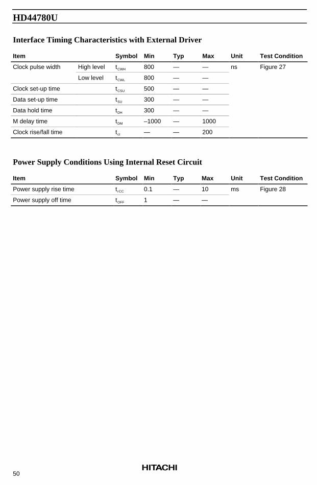
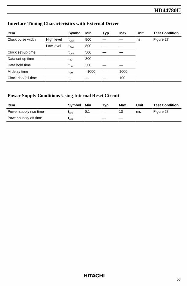
Interface Timing Characteristics with External Driver
Item Symbol Min Typ Max Unit Test Condition
Clock pulse width High level tCWH 800 — — ns Figure 27
Low level tCWL 800 — —
Clock set-up time tCSU 500 — —
Data set-up time tSU 300 — —
Data hold time tDH 300 — —
M delay time tDM –1000 — 1000
Clock rise/fall time tct — — 200
Power Supply Conditions Using Internal Reset Circuit
Item Symbol Min Typ Max Unit Test Condition
Power supply rise time t r CC 0.1 — 10 ms Figure 28
Power supply off time tOFF 1 — —
50

HD44780U
DC Characteristics (VCC = 4.5 to 5.5 V, Ta = –30 to +75°C*3)
Item Symbol Min Typ Max Unit Test Condition Notes*
Input high voltage (1)(except OSC1)
VIH1 2.2 — VCC V 6
Input low voltage (1)(except OSC1)
VIL1 –0.3 — 0.6 V 6
Input high voltage (2)(OSC1)
VIH2 VCC–1.0 — VCC V 15
Input low voltage (2)(OSC1)
VIL2 — — 1.0 V 15
Output high voltage (1)(DB0–DB7)
VOH1 2.4 — — V –IOH = 0.205 mA 7
Output low voltage (1)(DB0–DB7)
VOL1 — — 0.4 V IOL = 1.2 mA 7
Output high voltage (2)(except DB0–DB7)
VOH2 0.9 VCC — — V –IOH = 0.04 mA 8
Output low voltage (2)(except DB0–DB7)
VOL2 — — 0.1 VCC V IOL = 0.04 mA 8
Driver on resistance(COM)
RCOM — 2 20 kΩ ±Id = 0.05 mA,VLCD = 4 V
13
Driver on resistance(SEG)
RSEG — 2 30 kΩ ±Id = 0.05 mA,VLCD = 4 V
13
Input leakage current ILI –1 — 1 µA VIN = 0 to VCC 9
Pull-up MOS current(DB0–DB7, RS, R/W)
–Ip 50 125 250 µA VCC = 5 V
Power supply current ICC — 350 600 µA Rf oscillation,external clockVCC = 5 V,fOSC = 270 kHz
10, 14
LCD voltage VLCD1 3.0 — 11.0 V VCC–V5, 1/5 bias 16
VLCD2 3.0 — 11.0 V VCC–V5, 1/4 bias 16
Note: * Refer to the Electrical Characteristics Notes section following these tables.
51

HD44780U
AC Characteristics (VCC = 4.5 to 5.5 V, Ta = –30 to +75°C*3)
Clock Characteristics
Item Symbol Min Typ Max Unit Test Condition Notes*
External External clock frequency fcp 125 250 350 kHz 11clock External clock duty Duty 45 50 55 % 11operation
External clock rise time trcp — — 0.2 µs 11
External clock fall time tfcp — — 0.2 µs 11
Rf
oscillationClock oscillation frequency fOSC 190 270 350 kHz Rf = 91 kΩ
VCC = 5.0 V12
Note: * Refer to the Electrical Characteristics Notes section following these tables.
Bus Timing Characteristics
Write Operation
Item Symbol Min Typ Max Unit Test Condition
Enable cycle time tcycE 500 — — ns Figure 25
Enable pulse width (high level) PWEH 230 — —
Enable rise/fall time tEr, tEf — — 20
Address set-up time (RS, R/W to E) tAS 40 — —
Address hold time tAH 10 — —
Data set-up time tDSW 80 — —
Data hold time tH 10 — —
Read Operation
Item Symbol Min Typ Max Unit Test Condition
Enable cycle time tcycE 500 — — ns Figure 26
Enable pulse width (high level) PWEH 230 — —
Enable rise/fall time tEr, tEf — — 20
Address set-up time (RS, R/W to E) tAS 40 — —
Address hold time tAH 10 — —
Data delay time tDDR — — 160
Data hold time tDHR 5 — —
52
HD44780U
Interface Timing Characteristics with External Driver
Item Symbol Min Typ Max Unit Test Condition
Clock pulse width High level tCWH 800 — — ns Figure 27
Low level tCWL 800 — —
Clock set-up time tCSU 500 — —
Data set-up time tSU 300 — —
Data hold time tDH 300 — —
M delay time tDM –1000 — 1000
Clock rise/fall time tct — — 100
Power Supply Conditions Using Internal Reset Circuit
Item Symbol Min Typ Max Unit Test Condition
Power supply rise time trCC 0.1 — 10 ms Figure 28
Power supply off time tOFF 1 — —
53

HD44780U
Electrical Characteristics Notes
1. All voltage values are referred to GND = 0 V.
VCC
A
B
A 1.5 VB 0.25 × A ≥ ≤
The conditions of V1 and V5 voltages are for properoperation of the LSI and not for the LCD output level.The LCD drive voltage condition for the LCD outputlevel is specified as LCD voltage VLCD.
A =B =
VCC –V5VCC –V1
V1
V5
2. VCC ≥ V1 ≥ V2 ≥ V3 ≥ V4 ≥ V5 must be maintained.
3. For die products, specified at 75°C.
4. For die products, specified by the die shipment specification.
5. The following four circuits are I/O pin configurations except for liquid crystal display output.
PMOS
NMOS
VCC VCC
PMOS
NMOS
(pull up MOS)
PMOS
VCC
PMOS
NMOS
VCC
NMOS
NMOS
VCC
PMOS
NMOS
(output circuit)
Output enable Data
(pull-up MOS)
I/O PinPins: DB0 –DB7(MOS with pull-up)
Input pinPin: E (MOS without pull-up) Pins: RS, R/W (MOS with pull-up)
Output pinPins: CL1, CL2, M, D
VCC
(input circuit)
PMOSPMOS
Input enable
54
(tristate)

HD44780U
6. Applies to input pins and I/O pins, excluding the OSC1 pin.
7. Applies to I/O pins.
8. Applies to output pins.
9. Current flowing through pull–up MOSs, excluding output drive MOSs.
10. Input/output current is excluded. When input is at an intermediate level with CMOS, the excessivecurrent flows through the input circuit to the power supply. To avoid this from happening, the inputlevel must be fixed high or low.
11. Applies only to external clock operation.
Oscillator OSC1
OSC2
0.7 VCC0.5 VCC0.3 VCC
Th Tl
t rcp t fcp
Duty = 100%ThTh + Tl
×
Open
12. Applies only to the internal oscillator operation using oscillation resistor Rf.
OSC1
OSC2
Rf
R :R :
f
f
75 k ± 2% (when VCC = 3 V)91 k ± 2% (when VCC = 5 V)Ω
500
400
300
200
10050 100 150(91)
R (k )Ω
f
(k
Hz)
OS
C
VCC = 5 V500
400
300
200
10050 100 150
R (k )Ω
f
(k
Hz)
OS
C
VCC = 3 V
typ.
Since the oscillation frequency varies depending on the OSC1 and OSC2 pin capacitance, the wiring length to these pins should be minimized.
(270) (270)
Ω
(75)
typ.
max.
min.
max.
min.
55
f f
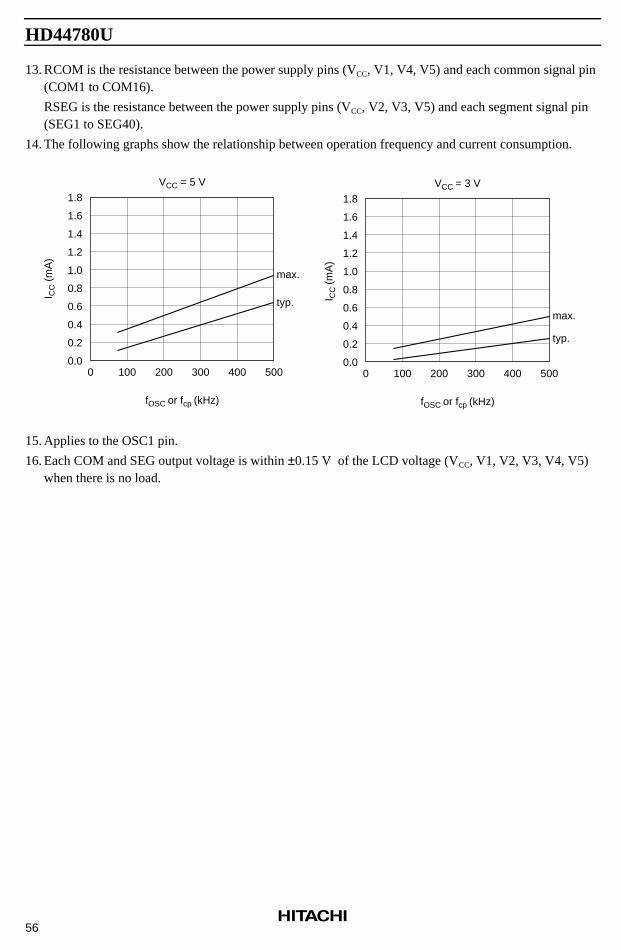
HD44780U
13. RCOM is the resistance between the power supply pins (VCC, V1, V4, V5) and each common signal pin(COM1 to COM16).
RSEG is the resistance between the power supply pins (VCC, V2, V3, V5) and each segment signal pin(SEG1 to SEG40).
14. The following graphs show the relationship between operation frequency and current consumption.
1.8
1.6
1.4
1.2
1.0
0.8
0.6
0.4
0.2
0.0
1.8
1.6
1.4
1.2
1.0
0.8
0.6
0.4
0.2
0.00 100 200 300 400 500
VCC = 5 V
0 100 200 300 400 500
VCC = 3 V
fOSC or fcp (kHz) fOSC or fcp (kHz)
I CC (
mA
)
I CC
(mA
)
max.
typ.max.
typ.
15. Applies to the OSC1 pin.
16. Each COM and SEG output voltage is within ±0.15 V of the LCD voltage (VCC, V1, V2, V3, V4, V5)
56
when there is no load.

HD44780U
Load Circuits
Data Bus DB0 to DB7
For V = 4.5 to 5.5 VCC
Testpoint
90 pF 11 kΩ
V = 5 VCC
3.9 kΩ
IS2074diodes
H
For V = 2.7 to 4.5 VCC
Testpoint
50 pF
External Driver Control Signals: CL1, CL2, D, M
Testpoint
30 pF
57
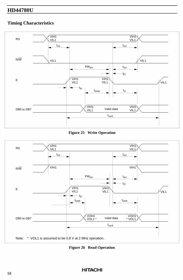
HD44780U
Timing Characteristics
RS
R/W
E
DB0 to DB7
VIH1VIL1
VIH1VIL1
tAS tAH
VIL1 VIL1
tAHPWEH
tEf
VIH1VIL1
VIH1VIL1
tErtDSW tH
VIH1VIL1
VIH1VIL1
tcycE
VIL1
Valid data
Figure 25 Write Operation
RS
R/W
E
DB0 to DB7
VIH1VIL1
VIH1VIL1
tAS tAH
VIH1 VIH1
tAHPWEH
tEf
VIH1VIL1
VIH1VIL1
tDDR tDHR
tEr
VIL1
VOH1VOL1 *
VOH1* VOL1Valid data
tcycE
Note: * VOL1 is assumed to be 0.8 V at 2 MHz operation.
58
Figure 26 Read Operation
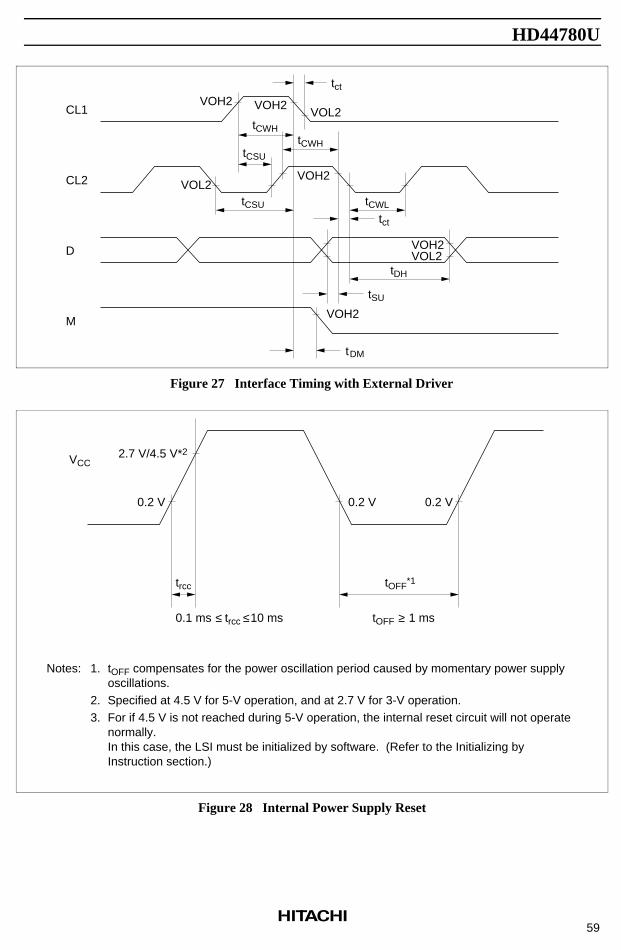
HD44780U
CL1
CL2
D
M
VOH2 VOH2VOL2
tct
tCWH
tCWH
tCSU
VOH2
tCSU tCWL
tct
tDH
tSU
VOH2
tDM
VOH2VOL2
VOL2
Figure 27 Interface Timing with External Driver
VCC
0.2 V
2.7 V/4.5 V*2
0.2 V 0.2 V
trcc tOFF*1
0.1 ms trcc 10 ms≤ ≤ tOFF 1 ms≥
Notes: 1.
2.3.
tOFF compensates for the power oscillation period caused by momentary power supply oscillations.Specified at 4.5 V for 5-V operation, and at 2.7 V for 3-V operation.For if 4.5 V is not reached during 5-V operation, the internal reset circuit will not operate normally. In this case, the LSI must be initialized by software. (Refer to the Initializing by Instruction section.)
59
Figure 28 Internal Power Supply Reset

HD44780U
Cautions
1. Hitachi neither warrants nor grants licenses of any rights of Hitachi’s or any third party’s patent,copyright, trademark, or other intellectual property rights for information contained in this document.Hitachi bears no responsibility for problems that may arise with third party’s rights, includingintellectual property rights, in connection with use of the information contained in this document.
2. Products and product specifications may be subject to change without notice. Confirm that you havereceived the latest product standards or specifications before final design, purchase or use.
3. Hitachi makes every attempt to ensure that its products are of high quality and reliability. However,contact Hitachi’s sales office before using the product in an application that demands especially highquality and reliability or where its failure or malfunction may directly threaten human life or cause riskof bodily injury, such as aerospace, aeronautics, nuclear power, combustion control, transportation,traffic, safety equipment or medical equipment for life support.
4. Design your application so that the product is used within the ranges guaranteed by Hitachi particularlyfor maximum rating, operating supply voltage range, heat radiation characteristics, installationconditions and other characteristics. Hitachi bears no responsibility for failure or damage when usedbeyond the guaranteed ranges. Even within the guaranteed ranges, consider normally foreseeablefailure rates or failure modes in semiconductor devices and employ systemic measures such as fail-safes, so that the equipment incorporating Hitachi product does not cause bodily injury, fire or otherconsequential damage due to operation of the Hitachi product.
5. This product is not designed to be radiation resistant.
6. No one is permitted to reproduce or duplicate, in any form, the whole or part of this document withoutwritten approval from Hitachi.
7. Contact Hitachi’s sales office for any questions regarding this document or Hitachi semiconductorproducts.
Hitachi, Ltd.Semiconductor & Integrated Circuits.Nippon Bldg., 2-6-2, Ohte-machi, Chiyoda-ku, Tokyo 100-0004, JapanTel: Tokyo (03) 3270-2111 Fax: (03) 3270-5109
Hitachi Asia Pte. Ltd.16 Collyer Quay #20-00Hitachi TowerSingapore 049318Tel: 535-2100Fax: 535-1533
URL NorthAmerica : http:semiconductor.hitachi.com/Europe : http://www.hitachi-eu.com/hel/ecgAsia (Singapore) : http://www.has.hitachi.com.sg/grp3/sicd/index.htmAsia (Taiwan) : http://www.hitachi.com.tw/E/Product/SICD_Frame.htmAsia (HongKong) : http://www.hitachi.com.hk/eng/bo/grp3/index.htmJapan : http://www.hitachi.co.jp/Sicd/indx.htm
Hitachi Asia Ltd.Taipei Branch Office3F, Hung Kuo Building. No.167, Tun-Hwa North Road, Taipei (105)Tel: <886> (2) 2718-3666Fax: <886> (2) 2718-8180
Hitachi Asia (Hong Kong) Ltd.Group III (Electronic Components)7/F., North Tower, World Finance Centre,Harbour City, Canton Road, Tsim Sha Tsui,Kowloon, Hong KongTel: <852> (2) 735 9218Fax: <852> (2) 730 0281 Telex: 40815 HITEC HXHitachi Europe Ltd.
Electronic Components Group.Whitebrook ParkLower Cookham RoadMaidenheadBerkshire SL6 8YA, United KingdomTel: <44> (1628) 585000Fax: <44> (1628) 778322
Hitachi Europe GmbHElectronic components GroupDornacher Straße 3D-85622 Feldkirchen, MunichGermanyTel: <49> (89) 9 9180-0Fax: <49> (89) 9 29 30 00
Hitachi Semiconductor (America) Inc.179 East Tasman Drive,San Jose,CA 95134 Tel: <1> (408) 433-1990Fax: <1>(408) 433-0223
For further information write to:
60
Copyright © Hitachi, Ltd., 1998. All rights reserved. Printed in Japan.