Harvesting Waste Energy: Bicycle Power Generation RIT-MSD-I Detailed Design Review Winter/Spring...
34
Harvesting Waste Energy: Bicycle Power Generation RIT-MSD-I Detailed Design Review Winter/Spring 2011-2012 P12414
-
Upload
leo-carson -
Category
Documents
-
view
226 -
download
0
Transcript of Harvesting Waste Energy: Bicycle Power Generation RIT-MSD-I Detailed Design Review Winter/Spring...

Harvesting Waste Energy:Bicycle Power Generation
RIT-MSD-I Detailed Design Review
Winter/Spring 2011-2012P12414

Team Members
• Daniel Tobin (ME)▫ Project Manager
• Amina Purak (ISE)▫ Facilitator
• Aaron Sieczkarek (ME)▫ Chief Engineer
• Brenda Lisitano (ME)
• Zheng (Flora) Li (EE)
GUIDE: Professor Brownell

Design Review Agenda•P

One Page Project Summary 1. Project Background
People in countries with inadequate infrastructure have an unmet need for electricity. A bicycle rotation energy harvesting system is a possible source for creating and storing power.
This system could provide the energy required for light, communication, or water treatment by converting kinetic energy to electrical energy for small electronic devices.
2. Problem Statement
Our goal is to transform kinetic energy within a bicycle into an electric power source intended to charge a cell phone. Our device is expected to be cheap to build, easy to install, maintain and use.

Customer Requirements

Specifications

Assembly

Motor SelectionVoltage Output Testing on the MIT device
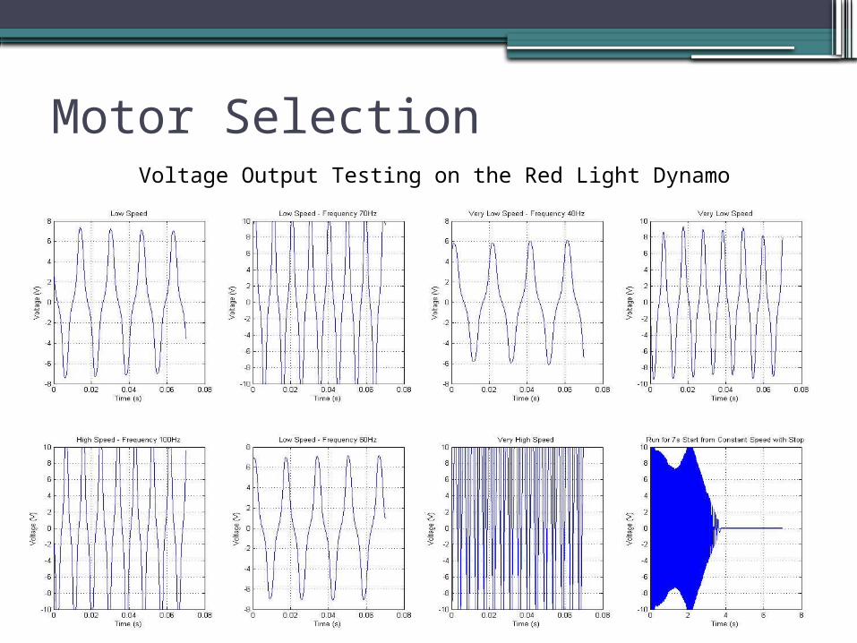
Motor SelectionVoltage Output Testing on the Red Light Dynamo

Motor SelectionVoltage Output Testing on the White Light Dynamo

Circuits Overview
C 1 14 7 0 u
-
+
12V DC motorTo Cell Phone
+
-
6V VoltageRegulator
Circuit Diagram for the MIT Device
The MIT device uses a 12 V DC motor, a 6V voltage regulator and a 470uF Capacitor. The circuit diagram is shown above.The function of this circuit is to stabilize the DC output from the DC motor and regulate it to a 6V constant output.

Circuits Overview• The voltage supplied by a USB port is nominally 5V. In practical, the
output is between 4.75V and 5.25V. A constant DC output of 5V is needed for the design.
Circuit
Non-linear oscillating
voltage inputConstant 5V DC
output
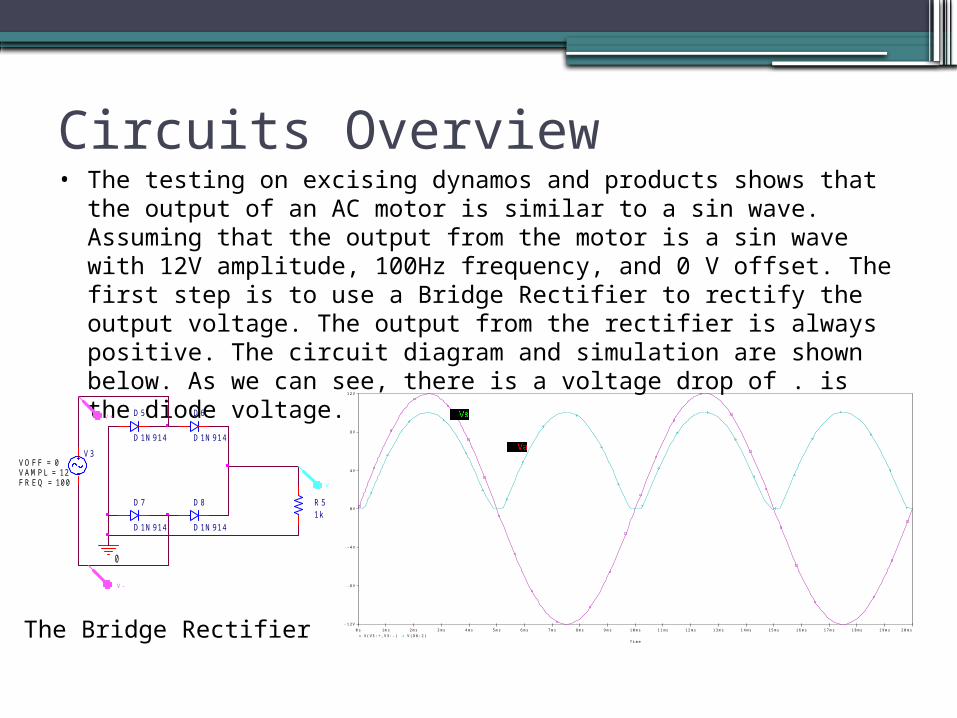
Circuits Overview• The testing on excising dynamos and products shows that the
output of an AC motor is similar to a sin wave. Assuming that the output from the motor is a sin wave with 12V amplitude, 100Hz frequency, and 0 V offset. The first step is to use a Bridge Rectifier to rectify the output voltage. The output from the rectifier is always positive. The circuit diagram and simulation are shown below. As we can see, there is a voltage drop of . is the diode voltage.
V 3
F R E Q = 1 0 0V A M P L = 1 2V O F F = 0
0
D 5
D 1 N 9 1 4
D 6
D 1 N 9 1 4
D 7
D 1 N 9 1 4
D 8
D 1 N 9 1 4
R 51 k
V
V-
V+
Time
0s 1ms 2ms 3ms 4ms 5ms 6ms 7ms 8ms 9ms 10ms 11ms 12ms 13ms 14ms 15ms 16ms 17ms 18ms 19ms 20msV(V3:+,V3:-) V(D8:2)
-12V
-8V
-4V
0V
4V
8V
12V
The Bridge Rectifier

Circuits Overview• The second step is stabilize the voltage output in a smaller range
then it is regulated to 5V constant DC output using a voltage regulator. The circuit diagram and simulations are shown. Capacitor C8 and C9 are used to additionally stabilize the voltage.
V 4
F R E Q = 1 0 0V A M P L = 1 2V O F F = 0
0
D 9
D 1 N 9 1 4
D 1 0
D 1 N 9 1 4
D 1 1
D 1 N 9 1 4
D 1 2
D 1 N 9 1 4
U 3L M 3 4 0 -5
I N1
O U T2
GN
D3
0
C 71 0 u
C 81 0 u
C 9. 1 u R 6
1 0 0 k
VV
Time
0s 1ms 2ms 3ms 4ms 5ms 6ms 7ms 8ms 9ms 10ms 11ms 12ms 13ms 14ms 15ms 16ms 17ms 18ms 19ms 20msV(D12:2) V(R6:2)
0V
2V
4V
6V
8V
10V
12V

Circuits Overview
Time
0s 1ms 2ms 3ms 4ms 5ms 6ms 7ms 8ms 9ms 10ms 11ms 12ms 13ms 14ms 15ms 16ms 17ms 18ms 19ms 20msV(V3:+,V3:-) V(D8:2) V(D12:2) V(R6:2)
-12V
-8V
-4V
0V
4V
8V
12V
Overall Waveform of the simulations
12V AC Positive Output
Positive Output in
Range5V DC
Cellphone
AC motor

Circuits Overview
V 4
F R E Q = 1 0 0V A M P L = 1 2V O F F = 0
0
D 9
D 1 N 9 1 4
D 1 0
D 1 N 9 1 4
D 1 1
D 1 N 9 1 4
D 1 2
D 1 N 9 1 4
U 3L M 3 4 0 -5
I N1
O U T2
GN
D3
0
C 71 0 u
C 81 0 u
C 9. 1 u R 6
1 0 0 k
D 1 4D 0 2 C Z 1 0
Additional Zener diode Circuit
As shown in circuit above, a 10V Zener diode is added. The Zener diode does not affect the function of the circuit. It is used to prevent high voltage input damage the voltage regulator. It is not necessary if the output of the motor is always lower than 25V.

Circuits Overview• At the end, after we get the 5V constant output. The
output pins will connect to a standard A-type USB connector. The pin 1 and 4 will be connected to the positive 5V pin and the ground of the circuit. The data transfer pins will also be grounded.
• Using the pin out below, all different kinds of USB to cellphone connectors can be made.

Circuits Overview• In the design process, we decided to use a DC motor instead of
an AC motor because of the price of the motors. The bridge rectifier is no longer necessary.
• Assume the 12V DC motor is used in our design. The output from the motor is approximately 5V DC voltage with ripples. The design shown below is used to regulate the voltage output.
C 81 0 u
12V DC motor C 9. 1 u
A-type USBConnector
4
1
U 4L M 3 4 0 -5
I N1
O U T2
GN
D3
0
C 71 0 u
Circuit diagram for 12V DC motor

Circuits Overview
Time
0s 1ms 2ms 3ms 4ms 5ms 6ms 7ms 8ms 9ms 10ms 11ms 12ms 13ms 14ms 15ms 16ms 17ms 18ms 19ms 20msV(V5:+,0) V(R9:2,0)
4V
5V
6V
7V
8V
9V
10V
11V
12V
13V
Time
0s 1ms 2ms 3ms 4ms 5ms 6ms 7ms 8ms 9ms 10ms 11ms 12ms 13ms 14ms 15ms 16ms 17ms 18ms 19ms 20msV(V5:+,0) V(R9:2,0)
4.8V
5.2V
5.6V
6.0V
6.4V
6.8V
7.2V
7.6V
8.0V
8.4V
Simulation of 12V DC motor with 12V motor output with ripples.
Simulation of 12V DC motor with 8V motor output with ripples.

Circuits Overview• Assume the waveform below is generated by a person riding
for 20s with two stops.
Time
0s 1s 2s 3s 4s 5s 6s 7s 8s 9s 10s 11s 12s 13s 14s 15s 16s 17s 18s 19s 20sV(V5:+,0) V(R9:2)
0V
2V
4V
6V
8V
10V
12V
• According to the simulation, the output of the circuit maintain at 5V when the motor’s output is between 6V to 12V.

BOM

Selected Parts Specs

Cost/Worth Analysis

Calculations …
Shaft Attachment
Motor Attachment

Box Attachment

RPM Calculation

Risks

Test Plan

Example Test Sheet

Gantt Chart for MSDII

Concerns Next Steps

We Welcome Your
Questions & Feedback