Hardware interfacing basics using AVR
146
Prepared by: Mohamed AbdAllah HW Interfacing Using AVR 1
-
Upload
mohamed-abdallah -
Category
Engineering
-
view
451 -
download
5
Transcript of Hardware interfacing basics using AVR

Prepared by: Mohamed AbdAllah
HW Interfacing
Using AVR
1

Agenda
Hardware Interfacing concept.
GPIO for simple I/O.
Polling vs. Interrupts.
Timer.
PWM (Pulse Width Modulation).
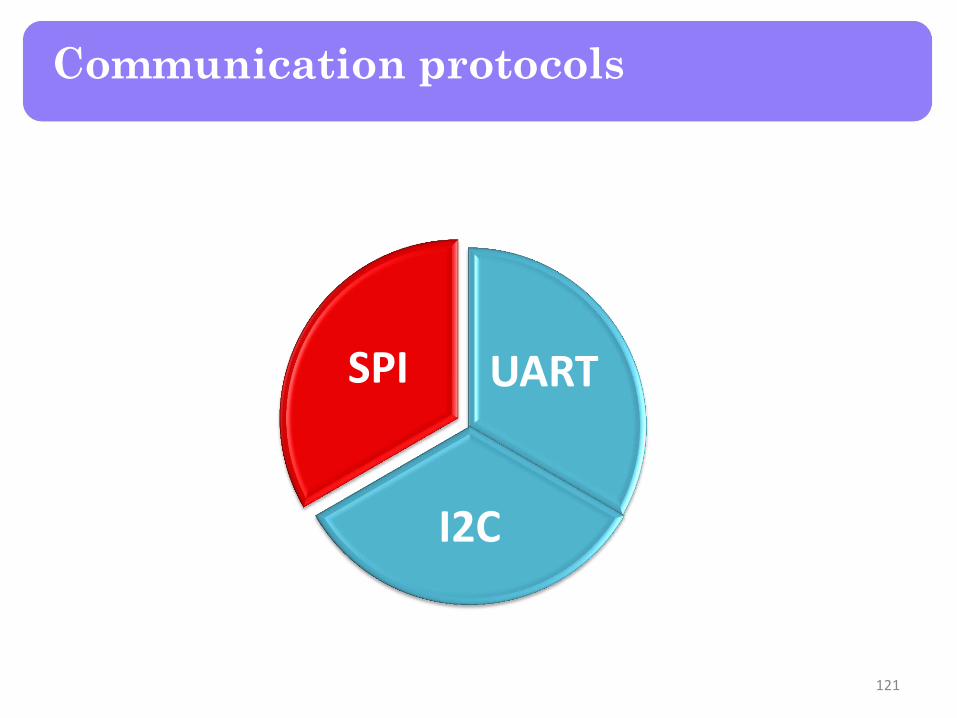
Communication protocols (UART, SPI, I2C).
ADC (Analog to Digital Converter).
2

Agenda
3

HW Interfacing concept
4

Embedded system is usually embedded as part of a complete device often including hardware and mechanical parts, which makes it necessary to make the embedded system micro-controller communicate (interface) with other parts of the complete system.
Hardware interfaces exist in many of the components such as the various buses, storage devices, other I/O devices, etc. A hardware interface is described by the mechanical, electrical and logical signals at the interface and the protocol for sequencing them.
5
HW Interfacing concept
sensor
switch
actuator
indicator

Important note
For all next slides we take only a specific examples on the ATMega16L, but you should read the full description of each module and its registers from the datasheet to know the full functionality of each module.
Read the datasheet
6
HW Interfacing concept

GPIO
7

What is GPIO
General-purpose input/output (GPIO) is a generic pin on an integrated circuit whose behavior -including whether it is an input or output pin- is controllable by the user at run time.
GPIO pins have no predefined purpose, and go unused by default.
Many embedded systems will provide a series of input/output pins for transmitting data from or to the outside world. These pins are arranged into groups called "ports". Ports will frequently (but not always) consist of a power-of-2 number of pins. For instance, common ports might be 4 pins, 8 pins, 16 pins, etc.
8
GPIO

What is GPIO
GPIO capabilities may include:
• GPIO pins can be configured to be input or output.
• GPIO pins can be enabled/disabled.
• Input values are readable (typically high=1, low=0).
• Output values are writable/readable.
• Input values can often be used as IRQs (Interrupt requests) (typically for wakeup events).
9
GPIO
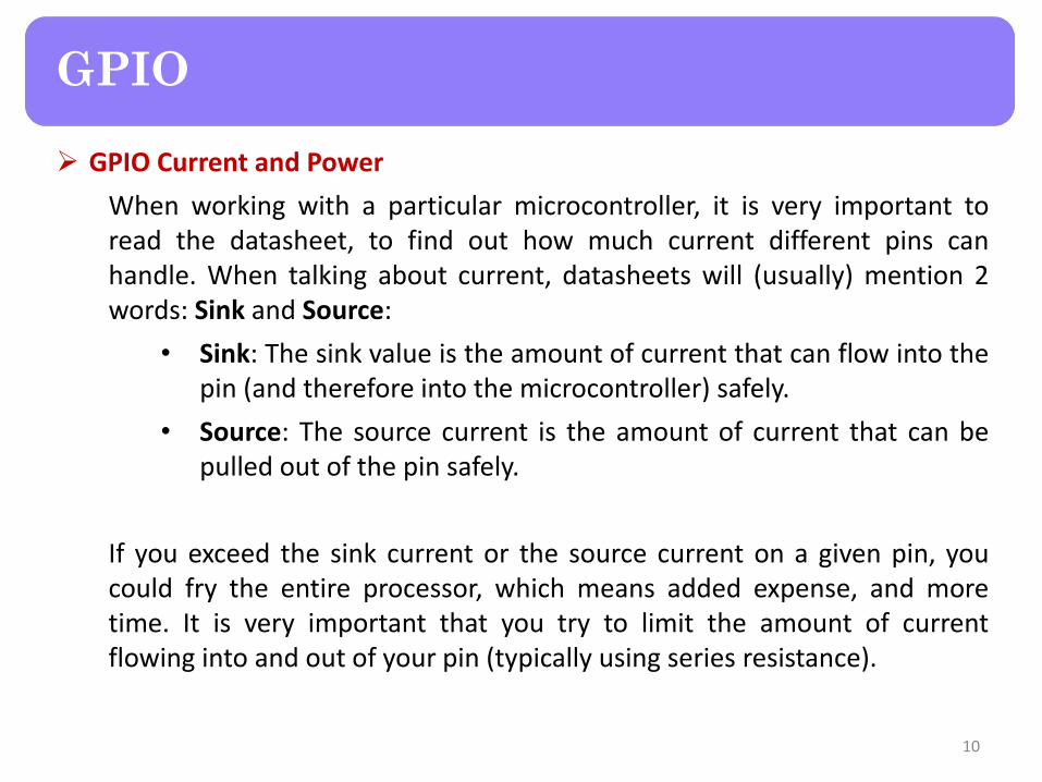
GPIO Current and Power
When working with a particular microcontroller, it is very important to read the datasheet, to find out how much current different pins can handle. When talking about current, datasheets will (usually) mention 2 words: Sink and Source:
• Sink: The sink value is the amount of current that can flow into the pin (and therefore into the microcontroller) safely.
• Source: The source current is the amount of current that can be pulled out of the pin safely.
If you exceed the sink current or the source current on a given pin, you could fry the entire processor, which means added expense, and more time. It is very important that you try to limit the amount of current flowing into and out of your pin (typically using series resistance).
10
GPIO

GPIO Ports for AVR – ATMega16L
ATMega16L has 32 programmable GPIO pins divided into 4 groups (ports) as appears in the picture:
11
GPIO

Memory mapping concept
Device drivers (Code that controls a particular type of device that is attached to your) communicate with peripheral devices through device registers (registers internal to each device).
A driver sends commands or data to a device by storing into its device register, or retrieves status or data from a device by reading from its device register.
The code can deal with these registers directly through assembly instructions, but it can’t do so directly with C code.
12
GPIO

Memory mapping concept
Many processors use memory-mapped I/O, which maps device registers to fixed addresses in the conventional memory space. To a C or C++ programmer, a memory-mapped device register looks very much like an ordinary data object. Programs can use ordinary assignment operators to move values to or from memory-mapped device registers.
By these memory mapped registers the C code can read or change the state of the device through its memory mapped registers.
Example on Arm-CortexM4 processor:
#define GPIO_PORTF_DATA_R (*((volatile unsigned long *)0x400253FC))
Previous line defined a macro to be used with PORTF register using its memory mapped address, then when typing:
GPIO_PORTF_DATA_R |= 0x01;
It will output logic high on pin0 of PORTF.
13
GPIO

Memory mapping concept
The same concept exists in our ATMega16L for different I/O registers, The first 96 locations of memory address the Register file and I/O Memory mapped registers, and the next 1024 locations address the internal data SRAM.
14
GPIO

Using GPIO
AVR is 8-bit microcontroller. All its ports are 8 bit wide. Every port has 3 registers associated with it each one with 8 bits. Every bit in those registers configure pins of particular port. Bit0 of these registers is associated with Pin0 of the port, Bit1 of these registers is associated with Pin1 of the port, and like wise for other bits.
These three registers are as follows (x can be replaced by A,B,C,D as per the AVR we are using) :
• DDRx register.
• PORTx register.
• PINx register.
15
GPIO

DDRx register
DDRx (Data Direction Register) configures data direction of port pins (input or output).
Configure pin as input: Write 0 to pin corresponding bit in DDRx.
Configure pin as output: Write 1 to pin corresponding bit in DDRx.
examples:
• to make all pins of PORTA as input pins :
DDRA = 0b00000000;
• to make all pins of PORTA as output pins :
DDRA = 0b11111111;
• to make lower nibble of PORTB as output and higher nibble as input :
DDRB = 0b00001111;
16
GPIO

Burn the code to controller
The process of putting your code on the controller is called Burning or Flashing, this step happens after compiling your code (You can download and use Atmel Studio IDE to write and compile your code), and is done using a special hardware to connect your controller to your PC (Search internet for USBasp) and a special software program on your PC (Search internet for eXtreme burner or any other software).
You can search the internet for tutorials about using each of aforementioned HW/SW as it differs depending on the used hardware and software and will not be covered here.
17
GPIO

PINx register
PINx (Port IN) used to read data from port pins. In order to read the data from port pin, first you have to change port’s data direction to input. This is done by setting bits in DDRx to zero. If port is made output, then reading PINx register will give you data that has been output on port pins.
Now there are two input modes. Either you can use port pins as tri stated inputs or you can activate internal pull up. It will be explained shortly.
example :
• to read data from PORTA.
DDRA = 0x00; //Set PORTA as input
x = PINA; //Read contents of PORTA
18
GPIO

PINx register
Pin can be connected through external pull up/down resistors as shown:
19
GPIO
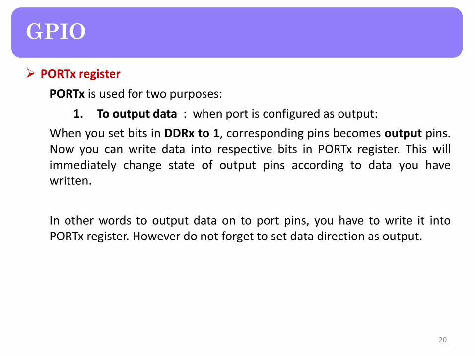
PORTx register
PORTx is used for two purposes:
1. To output data : when port is configured as output:
When you set bits in DDRx to 1, corresponding pins becomes output pins. Now you can write data into respective bits in PORTx register. This will immediately change state of output pins according to data you have written.
In other words to output data on to port pins, you have to write it into PORTx register. However do not forget to set data direction as output.
20
GPIO

PORTx register
examples:
• to output 0xFF data on PORTB
DDRB = 0b11111111; //set all pins of PORTB as outputs
PORTB = 0xFF; //write data on PORTB
• to output data in variable x on PORTA
DDRA = 0xFF; //make PORTA as output
PORTA = x; //output variable on PORTA
• to output data on only pin2 of PORTC
DDRC |= 1 << 2; //set only pin2 of PORTC as output
PORTC |= 1 << 2; //make it high.
21
GPIO

PORTx register
2. To activate/deactivate pull up resistors: when port is configured as input:
When you set bits in DDRx to 0, i.e. make port pins as inputs, then corresponding bits in PORTx register are used to activate/deactivate pull-up registers associated with that pin. In order to activate pull-up resister, set bit in PORTx to 1, and to deactivate (i.e to make port pin tri stated) set it to 0.
22
GPIO
PORTx register
In input mode, when pull-up is enabled, default state of pin becomes ‘1’. So even if you don’t connect anything to pin and if you try to read it, it will read as 1. Now, when you externally drive that pin to zero(i.e. connect to ground / or pull-down), only then it will be read as 0.
However, if you configure pin as tri state. Then pin goes into state of high impedance. We can say, it is now simply connected to input of some OpAmp inside the uC and no other circuit is driving it from uC. Thus pin has very high impedance. In this case, if pin is left floating (i.e. kept unconnected) then even small static charge present on surrounding objects can change logic state of pin. If you try to read corresponding bit in pin register, its state cannot be predicted. This may cause your program to go haywire, if it depends on input from that particular pin.
Thus while taking inputs from pins using micro-switches to take input, always enable pull-up resistors on input pins.
23
GPIO
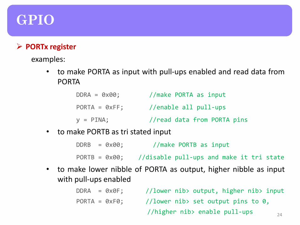
PORTx register
examples:
• to make PORTA as input with pull-ups enabled and read data from PORTA
DDRA = 0x00; //make PORTA as input
PORTA = 0xFF; //enable all pull-ups
y = PINA; //read data from PORTA pins
• to make PORTB as tri stated input
DDRB = 0x00; //make PORTB as input
PORTB = 0x00; //disable pull-ups and make it tri state
• to make lower nibble of PORTA as output, higher nibble as input with pull-ups enabled
DDRA = 0x0F; //lower nib> output, higher nib> input
PORTA = 0xF0; //lower nib> set output pins to 0,
//higher nib> enable pull-ups 24
GPIO

Notes
• To use the GPIO features inside AtmelStudio, avr/io.h header file should be included.
• To use the delay feature, util/delay.h header file should be included, then we can write:
_delay_ms(1000); //Delay 1 second
_delay_us(100); //Delay 100 micro second
25
GPIO

Polling vs. Interrupts
26

Polling vs. Interrupt
A single microcontroller can serve several devices, there are two ways to do that: interrupts or polling
• Polling: In the Polling method, the microcontroller must "access by himself" the device and “ask” for the information it needs for processing. In fact we see that in the Polling method the external devices are not independent systems, they depend on the microcontroller, and only the micro is entitled to obtain access to the information it needs.
The main drawback of this method when writing program is waste of time of microcontroller, which needs to wait and check whether the new information has arrived.
The microcontroller continuously monitors the status of a given device until required information is ready. After that, it moves on to monitor the next device until everyone is serviced. The microcontroller checks all devices in a round robin fashion.
27
Polling vs. Interrupts

Polling vs. Interrupt
• Interrupt: Interrupt is the signal sent to the micro to mark the event that requires immediate attention.
Interrupt is “requesting" the processor to stop performing the current program and to “make time” to execute a special code. Whenever any device needs its service, the device notifies the microcontroller by sending it an interrupt signal.
Upon receiving an interrupt signal, the microcontroller interrupts whatever it is doing and serves the device. The program which is associated with the interrupt is called the interrupt service routine (ISR) or interrupt handler.
28
Polling vs. Interrupts

Polling vs. Interrupt
29
Is info ready
?
No
yes
Process information
Polling Interrupt
Polling vs. Interrupts

Polling vs. Interrupt on ATMega16L
Polling and interrupts concept exists on AVR not only for the GPIO but also for other modules as illustrated later.
The previous method of handling GPIO input was “Polling” as the user asks explicitly for the PINx state.
In the “Interrupt” mode the user will not ask for the PINx state, but instead configures the input pin to work in interrupt mode, then when the pin state changes the program stops execution then the corresponding ISR will be called then after the ISR finishes, the program will continue execution from were it was left.
30
Polling vs. Interrupts
Interrupt Vector Table (IVT)
An interrupt vector table (IVT) is a data structure that associates a list of interrupt handlers with a list of interrupt requests in a table of interrupt vectors. An entry in the interrupt vector is the address of the interrupt handler.
So when interrupt occurs, depending on which interrupt occurred (interrupt request), the processor takes from the IVT the address of the ISR that it will jump to.
If multiple interrupts occurred on the same time, the CPU handles the higher priority interrupt, which in the AVR is determined from the ISR location inside the IVT, the first entry is the highest interrupt (Reset interrupt) as shown in the flowing table.
Note: to use the AVR interrupt functionality, avr/interrupt.h header file should be included.
31
Polling vs. Interrupts
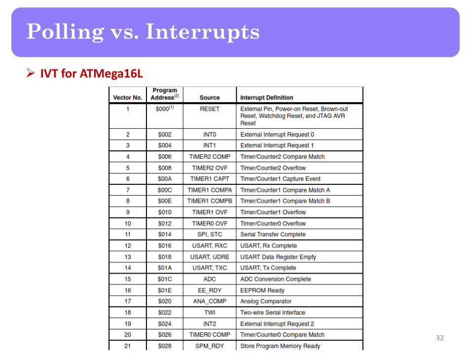
IVT for ATMega16L
32
Polling vs. Interrupts

Pins with interrupt mode
33
Polling vs. Interrupts

Steps to work with GPIO interrupts
1. Disable global interrupts:
Inside SREG register (status register), there is a bit to enable/disable all interrupts in the AVR, at initialization it is better to disable all interrupts to avoid unexpected interrupts behavior, then enable it again after initialization steps:
Note that SREG register contains other useful information about the result of the most recently executed arithmetic instruction (carry flag, zero flag, etc…). This information can be used for altering program flow in order to perform conditional operations.
34
Polling vs. Interrupts

Steps to work with GPIO interrupts
1. Disable global interrupts:
To disable the global interrupt, the I-bit should be cleared:
SREG &= ~(1<<7);
OR: we can use the built in macro:
cli();
35
Polling vs. Interrupts

Steps to work with GPIO interrupts
2. Make the corresponding pin to be input:
To work with INT0 (PD2):
DDRD &= ~(1<<3);
3. Choose pin interrupt mode of operation:
For INT0 and INT1, use the MCUCR register:
36
Polling vs. Interrupts

Steps to work with GPIO interrupts
3. Choose pin interrupt mode of operation:
37
Polling vs. Interrupts
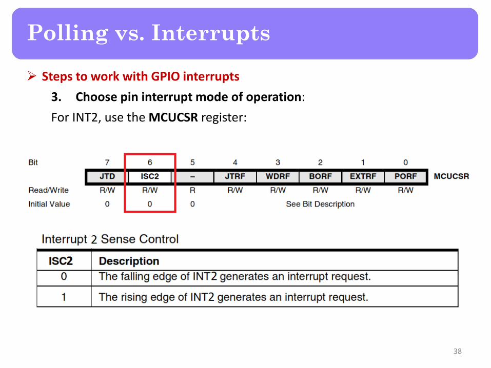
Steps to work with GPIO interrupts
3. Choose pin interrupt mode of operation:
For INT2, use the MCUCSR register:
38
Polling vs. Interrupts

Steps to work with GPIO interrupts
4. Enable the required interrupt:
The required interrupt (ex. INT0) should be enabled, this is done through GICR register, writing 1 to the bit enable the interrupt:
Example: to enable INT0 only:
GICR |= 1<<6;
39
Polling vs. Interrupts

Steps to work with GPIO interrupts
5. Enable global interrupts:
To enable the global interrupt, the I-bit should be set to 1:
SREG |= 1<<7;
OR: we can use the built in macro:
sei();
40
Polling vs. Interrupts

Steps to work with GPIO interrupts
6. Write your ISR body for the required INTx:
For example, to write the INT0 ISR body:
ISR(INT0_vect) {
Flag = 1; /* Any short code */
}
41
Polling vs. Interrupts

Nested interrupts
After any interrupt occurs, the I-bit is cleared automatically when entering the ISR and set to 1 automatically when leaving the ISR.
If nested interrupts is enabled, the interrupt behavior will be as follows:
42
Polling vs. Interrupts

Nested interrupts
To enable the nested interrupts, set the I-bit inside the ISR itself, so if any other higher priority interrupt occurred, the current ISR will be interrupted also and another ISR will be called, then after the second ISR finishes the control goes back to the first ISR to continue, then after that to the original interrupted code.
ISR(INT0_vect) {
sei(); /* Then Any short code */
}
But this still leaves few instructions inside the compiler-generated function prologue to run with global interrupts disabled. The compiler can be instructed to insert an SEI instruction right at the beginning of an interrupt handler by declaring the handler the following way:
ISR(INT0_vect, ISR_NOBLOCK) {
/* Any short code */
} 43
Polling vs. Interrupts

Timer
44

What is a timer ?
A timer in simplest term is a register. Timers generally have a resolution of 8 or 16 Bits. So a 8 bit timer is 8Bits wide so capable of holding value within 0-255. But this register has a special property, Its value increases/decreases automatically at a predefined rate (supplied by user). This is the timer clock. And this operation does not need CPU’s intervention.
Since Timer works independently of CPU it can be used to measure time accurately. Timer upon certain conditions take some action automatically or inform CPU. One of the basic condition is the situation when timer overflows i.e. it counts up to its maximum value (255 for 8-bit timers) and rolled back to 0. In this situation timer can issue an interrupt and you must write an Interrupt Service Routine (ISR) to handle the event.
45
Timer

Timers in ATMega16L
In ATMega16L we have three different kinds of timers:
• TIMER0: 8-bit timer.
• TIMER1: 16-bit timer.
• TIMER2: 8-bit timer.
The best part is that the timer is totally independent of the CPU. Thus, it runs parallel to the CPU and there is no CPU’s intervention, which makes the timer quite accurate.
Apart from normal operation, these three timers can be either operated in normal mode (Timer is cleared after it overflows), CTC mode (Timer is cleared after matching a specific value) or PWM mode (Will be discussed later). We will discuss them one by one.
46
Timer

Timer frequency
Using time-frequency formula:
𝑇𝑖𝑚𝑒 𝑝𝑒𝑟𝑖𝑜𝑑 = 1
𝐹𝑟𝑒𝑞𝑢𝑒𝑛𝑐𝑦
Now suppose, we need to flash an LED every 10 ms. This implies that its frequency is 1/10ms = 100 Hz. Now let’s assume that we have an external crystal XTAL of 4 MHz. Hence, the CPU clock frequency is 4 MHz. Now, as we said that the timer counts from 0 to TOP. For an 8-bit timer, it counts from 0 to 255 whereas for a 16-bit timer it counts from 0 to 65535. After that, they overflow. This value changes at every clock pulse.
47
Timer

Timer frequency
Let’s say the timer’s value is zero now. To go from 0 to 1, it takes one clock pulse. To go from 1 to 2, it takes another clock pulse. To go from 2 to 3, it takes one more clock pulse. And so on. For CPU frequency F_CPU = 4 MHz, time period T = 1/4M = 0.00025 ms. Thus for every transition (0 to 1, 1 to 2, etc), it takes only 0.00025 ms!
Now, as stated above, we need a delay of 10 ms. This maybe a very short delay, but for the microcontroller which has a resolution of 0.00025 ms, its quite a long delay! To get an idea of how long it takes, let’s calculate the timer count from the following formula:
𝑇𝑖𝑚𝑒𝑟 𝑐𝑜𝑢𝑛𝑡 = 𝑅𝑒𝑞𝑢𝑖𝑟𝑒𝑑 𝑑𝑒𝑙𝑎𝑦
𝐶𝑙𝑜𝑐𝑘 𝑡𝑖𝑚𝑒 𝑝𝑒𝑟𝑖𝑜𝑑 − 1
The -1 is for the fact that timer starts from zero not 1.
48
Timer

Timer frequency
Substitute Required Delay = 10 ms and Clock Time Period = 0.00025 ms, and you get Timer Count = 39999. The clock has already ticked 39999 times to give a delay of only 10 ms !
Now, to achieve this, we definitely cannot use an 8-bit timer (as it has an upper limit of 255, after which it overflows). Hence, we use a 16-bit timer (which is capable of counting up to 65535) to achieve this delay.
49
Timer

Using prescaler
Assuming F_CPU = 4 MHz and a 16-bit timer (MAX = 65535), and substituting in the above formula, we can get a maximum delay of 16.384 ms. Now what if we need a greater delay, say 20 ms? We are stuck.
Hopefully, there lies a solution to this. Suppose if we decrease the F_CPU from 4 MHz to 0.5 MHz (i.e. 500 kHz), then the clock time period increases to 1/500k = 0.002 ms. Now if we substitute Required Delay = 20 ms and Clock Time Period = 0.002 ms, we get Timer Count = 9999. As we can see, this can easily be achieved using a 16-bit timer. At this frequency, a maximum delay of 131.072 ms can be achieved.
This technique of frequency division is called prescaling. We do not reduce the actual F_CPU. The actual F_CPU remains the same (at 4 MHz in this case). So basically, we derive a frequency from it to run the timer. Thus, while doing so, we divide the frequency and use it.
50
Timer

Using prescaler
But prescaler comes at a cost. There is a trade-off between resolution and duration.
As we have seen above, the overall duration of measurement has increased from 16.384 ms to 131.072 ms. So has the resolution. The resolution has also increased from 0.00025 ms to 0.002 ms (technically the resolution has actually decreased). This means each tick will take 0.002 ms.
So, what’s the problem with this? The problem is that the accuracy has decreased. Earlier, you were able to measure duration like 0.1125 ms accurately (0.1125/0.00025 = 450), but now we cannot (0.1125/0.002 = 56.25). The new timer can measure 0.112 ms and then 0.114 ms. No other value in between.
51
Timer

Choosing prescaler value
Let’s take an example. We need a delay of 184 ms (Any random number). We have F_CPU = 4 MHz. The AVR offers us the following prescaler values to choose from: 8, 64, 256 and 1024. A prescaler of 8 means the effective clock frequency will be F_CPU/8. Now substituting each of these values into the above formula, we get different values of timer value. The results are summarized as below:
52
Timer
prescaler Clock frequency Timer count
8 500 KHz 91999
64 62.5 KHz 11499
256 15.625 KHz 2874
1024 3906.25 Hz 717.25

Choosing prescaler value
Now out of these four prescalers, 8 cannot be used as the timer value exceeds the limit of 65535. Also, since the timer always takes up integer values, we cannot choose 1024 as the timer count is a decimal digit. Hence, we see that prescaler values of 64 and 256 are feasible. But out of these two, we choose 64 as it provides us with greater resolution. We can choose 256 if we need the timer for a greater duration elsewhere.
Thus, we always choose prescaler which gives the counter value within the feasible limit (255 or 65535) and the counter value should always be an integer.
Sometimes we don’t find any prescaler that gives integer counter value, which means that the timing will not be very accurate then.
53
Timer

Working with TIMER0 steps
We will take TIMER0 as an example, we will work in CTC mode (Clear Timer on Compare match) with interrupt enabled.
Thus, we always choose prescaler which gives the counter value within the feasible limit (255 or 65535) and the counter value should always be an integer.
Sometimes we don’t find any prescaler that gives integer counter value, which means that the timing will not be very accurate then.
54
Timer

Working with TIMER0 steps
1. Disable global interrupts.
2. Initialize Timer/Counter0 value to be 0:
This is the initial actual timer value, we want to start from 0, and this register is incremented each timer clock:
TCNT0 = 0;
55
Timer

Working with TIMER0 steps
3. Set the required compare value:
Set the compare value that we need to always compare to it after each timer count:
OCR0 = 230; /* We want to stop counting at 230 */
56
Timer

Working with TIMER0 steps
4. Enable the required interrupt:
The required interrupt for CTC mode should be enabled, this is done through TIMSK register, writing 1 to the bit enable the interrupt:
TIMSK |= (1<<OCIE0);
57
Timer

Working with TIMER0 steps
5. Enable global interrupts.
6. Set Timer0 operation mode and set the prescaler value, this will start timer counting:
From the data sheet we can find that we must:
• Set FOC0 to operate in none PWM mode (PWM will be discussed later).
• Set WGM01 to operate in CTC mode.
• Set CS00 and CS02 to set the prescaler to be 1024 after this step the timer will start counting.
58
Timer

Working with TIMER0 steps
The step in one line of code:
TCCR0 = (1<<FOC0) | (1<<WGM01) | (1<<CS00) | (1<<CS02);
59
Timer

Working with TIMER0 steps
7. Write your ISR body for TIMER0:
ISR(TIMER0_COMP_vect) {
/* Any short code */
}
Note: If we set the CS00:02 to be all zeros, this will disconnect the clock from the timer which means stopping the timer from counting.
60
Timer

PWM
61

What is PWM?
• Pulse-width modulation (PWM), or pulse-duration modulation (PDM), is a
technique for getting analog results with digital means.
Digital control is used to create a square wave, a signal switched between ON
and OFF. This ON-OFF pattern can simulate voltages in between full ON (5
Volts) and OFF (0 Volts) by changing the portion of the time the signal spends
ON versus the time that the signal spends OFF. The duration of “ON time" is
called the pulse width. To get varying analog values, you change, or
modulate, that pulse width. If you repeat this ON-OFF pattern fast enough
with an LED for example, the result is as if the signal is a steady voltage
between 0 and 5v controlling the brightness of the LED. 62
PWM

What is PWM?
• The average value of voltage (and current) fed to the load is controlled by
turning the switch between supply and load ON and OFF at a fast rate.
The longer the switch is ON compared to the OFF periods, the higher the
total power supplied to the load.
For the 0-5V example, if ON duration is 75% of the period, then if we
connected a LED it will feel like as if it is 3.75V (75% * 5V).
63
PWM

What is PWM?
• The PWM switching frequency has to be much higher than what would
affect the load (the device that uses the power), which is to say that the
resultant waveform perceived by the load must be as smooth as possible.
Typically switching has to be done several times a minute in an electric
stove, 120 Hz in a lamp dimmer, from few kilohertz (kHz) to tens of kHz
for a motor drive and well into the tens or hundreds of kHz in audio
amplifiers and computer power supplies.
64
PWM
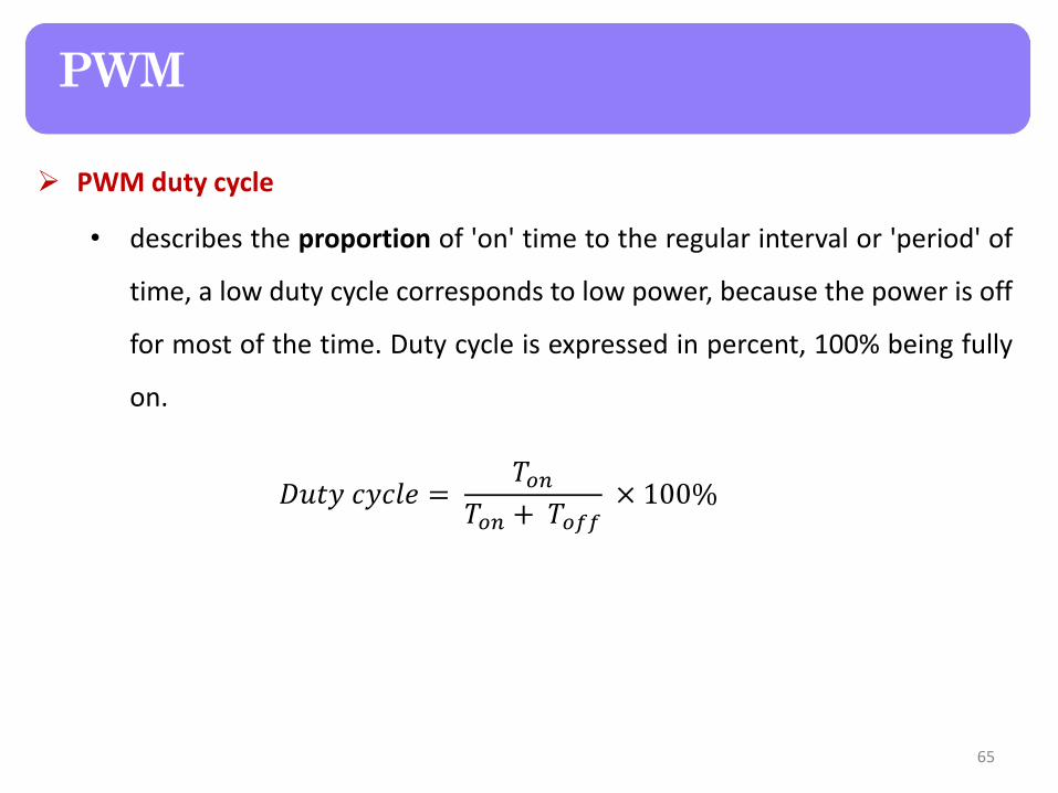
PWM duty cycle
• describes the proportion of 'on' time to the regular interval or 'period' of
time, a low duty cycle corresponds to low power, because the power is off
for most of the time. Duty cycle is expressed in percent, 100% being fully
on.
𝐷𝑢𝑡𝑦 𝑐𝑦𝑐𝑙𝑒 = 𝑇𝑜𝑛
𝑇𝑜𝑛 + 𝑇𝑜𝑓𝑓 × 100%
65
PWM

PWM duty cycle
66
PWM

Fast PWM mode in ATMega16L as an example
ATMega16L has many ways to generate PWM signal, we will take “Fast PWM” as an example.
We will be using one of our timers (TIMER0 as our example) to count and the counter value will determine which signal to send on a specific bin High or Low.
PWM signal can be generated in two forms, inverted and non-inverted:
• Inverted PWM: Signal is Low till reaching a compare match then it is inverted to High till reaching the TOP value of the timer then inverted to low and repeats again.
• Non-inverted PWM: Signal is High till reaching a compare match then it is inverted to Low till reaching the TOP value of the timer then inverted to low and repeats again.
67
PWM

Fast PWM mode in ATMega16L as an example
68
PWM
Timer
Inverted
Non-inverted

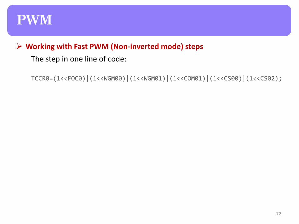
Working with Fast PWM (Non-inverted mode) steps
1. Set PB3 as output:
We will be working with OC0 output pin which is on PB3, so we need to set this pin as output first:
DDRB |= (1<<PINB3);
2. Initialize Timer/Counter0 value to be 0:
This is the initial actual timer value, we want to start from 0:
TCNT0 = 0;
69
PWM

Working with Fast PWM (Non-inverted mode) steps
3. Set the required compare value:
Set the compare value that we need to always compare to it after each timer count, not that now after a compare match the timer will continue counting up till reaching TOP value, not like CTC mode that clears the timer after compare match, this way operation is the reason that we can output PWM signal.
The OCR0 value is determined in Non-inverted mode by the following formula:
𝑂𝐶𝑅0 = 𝐷𝑢𝑡𝑦 𝑐𝑦𝑐𝑙𝑒
100 × 255
We multiplied by 255 as we will use TIMER0 which has a maximum of 255 count, and we want to know how many ticks we need to go before clearing the PWM signal to LOW.
Duty cycle can have any value from 0 to 100, note that doing this equation in code on integer operations may lead to zero value so do it on float or do the multiply first.
70
PWM

Working with Fast PWM (Non-inverted mode) steps
4. Set Timer0 operation mode and set the prescaler value, this will start timer counting:
From the data sheet we can find that we must:
• Set FOC0 also in PWM mode (required from datasheet).
• Set WGM00 and WGM01 to operate in Fast PWM mode.
• Set COM01 to clear OC0 on compare match (Non-inverted PWM).
• Set CS00 and CS02 to set the prescaler to be 1024 after this step the timer will start counting.
71
PWM
Working with Fast PWM (Non-inverted mode) steps
The step in one line of code:
TCCR0=(1<<FOC0)|(1<<WGM00)|(1<<WGM01)|(1<<COM01)|(1<<CS00)|(1<<CS02);
72
PWM

In Normal Mode, the timer triggers interrupt handlers. These can do practically any function you want, but the ISR runs on the CPU, which prevents anything else from running at the same time.
In CTC mode, you can also trigger interrupts, but it is also possible not to use interrupts and still toggle an output pin (OC0 for example). Using it this way, the functionality occurs parallel to the CPU and doesn't interrupt anything.
PWM runs in the background like CTC, but the timing of the output on the pin is different. It is more suited to devices like servos that take pulse-width modulation as input as we can choose any duty cycle (Not only 50% like OC0 toggle in CTC mode).
73
Timer and PWM summary

Communication protocols
74

What is communication in embedded systems ?
• It is a way of exchanging data or commands between 2 or more different
embedded systems devices.
• Communication protocols are standards that contains data exchange
rules and format between embedded systems.
Communication protocols examples in embedded systems
• UART.
• I2C.
• SPI.
• CAN.
• LIN.
75
Communication protocols

Bit rate
• It is the number of bits that are sent per unit of time usually bits/sec.
Baud rate
• It is the number of symbols that are sent per unit of time usually, symbol
can be combination of any number of bits according to design choice.
• In case that symbol is only 1 bit, then baud rate will equal the bit rate.
76
Communication protocols

Serial communication
Sending bit by bit.
Parallel Communication
Sending multiple bits simultaneously.
77
Communication protocols

78
Communication protocols

Synchronous serial communication
• Synchronous serial communication describes a serial communication
protocol in which data is sent in a continuous stream at a constant rate.
• Synchronous communication requires that the clocks in the transmitting
and receiving devices are synchronized – running at the same rate – so
the receiver can sample the signal at the same time intervals used by the
transmitter so that there is an extra wire for clock carrying.
Sender Receiver
Tx
Rx
Clck
79
Communication protocols

Asynchronous serial communication
• Asynchronous serial communication is a form serial communication in
which the communicating endpoints' interfaces are not continuously
synchronized by a common clock signal.
• Instead of a common synchronization signal, the data stream contains
synchronization information in form of start and stop signals, before and
after each unit of transmission, respectively. The start signal prepares the
receiver for arrival of data and the stop signal resets its state to enable
triggering of a new sequence.
Sender Receiver
Tx
Rx 80
Communication protocols

UART
I2C
SPI
81
Communication protocols

UART
I2C
SPI
82
Communication protocols

What is UART ?
• UART stands for Universal Asynchronous Receiver Transmitter. There is
one wire for transmitting data, and one wire to receive data. A common
parameter is the baud rate known as "bps" which stands for bits per
second. If a transmitter is configured with 9600bps, then the receiver
must be listening on the other end at the same speed.
• UART is a serial communication, so bits must travel on a single wire. If you
wish to send a char (8-bits) over UART, the char is enclosed within a start
and a stop bit, so to send 8-bits of char data, it would require 2-bit
overhead, this 10-bit of information is called a UART frame.
83
Communication protocols

UART frame format
84
Communication protocols

UART frame format
• Start bit: 1 bit indicates the start of a new frame, always logic low.
• Data: 5 to 9 bits of sent data.
• Parity bit: 1 bit for error checking
Even parity: clear parity bit if number of 1s sent is even.
Odd parity: clear parity bit if number of 1s sent is odd.
• Stop bit: 1 or 2 bits indicate end of frame, always logic high.
85
Communication protocols

UART notes
• UART supports PC communication through RS232.
• UART standard baud rate examples (110, 300, 600, 1200, 4800, 9600, ....).
• UART is a full duplex communication protocol.
• UART is point to point communication protocol, which means
communication can be between 2 devices only at the same time.
86
Communication protocols

UART/USART on ATMega16L
ATMega16L supports both normal UART and also USART (Universal Synchronous Asynchronous Receiver/Transmitter) which is the same like UART concepts except that it also supports Synchronous mode through external clock.
It also supports working in polling or interrupt modes for UART Tx and Rx.
We will take UART as an example and we will work in polling mode.
87
Communication protocols

Working with UART steps
1. Set transfer rate mode:
AVR supports 2 different transfer modes: normal and double transfer modes, they differ only in the calculations of the baud rate as follows:
88
Communication protocols

Working with UART steps
Setting the transfer mode is through the U2X bit inside the UCSRA register:
UCSRA |= (1<<U2X);
89
Communication protocols

Working with UART steps
2. Enable Tx and Rx:
Enable the transmitter and receiver through UCSRB register:
UCSRB |= (1<<TXEN) | (1<<RXEN);
90
Communication protocols

Working with UART steps
3. Setup the UART frame:
From the data sheet we can find that we must:
• Set URSEL when writing to UCSRC register.
• Set UCSZ0 and UCSZ1 for 8-bits data frame.
• Clear UMSEL to operate in Asynchronous mode.
• Clear UPM0 and UPM1 to for zero parity bits frame.
• Clear USBS for 1 stop bit frame.
91
Communication protocols

Working with UART steps
The step in one line of code:
UCSRC |= (1<<URSEL) | (1<<UCSZ1) | (1<<UCSZ0);
4. Start sending data:
To start sending data, at each byte we want to send we should wait first until making sure that previous byte was sent (polling mode), then start sending another byte. This is done through polling on UDRE bit inside UCSRA register, when transmitter is ready to send new data the UDRE bit is set to 1.
After making sure that UDRE bit is high, we can start sending through writing the required byte to send inside the UDR register:
while (!((UCSRA) & (1<<UDRE)));
UDR = ‘A’; /* Send A through UART */
92
Communication protocols

Working with UART steps
5. Start receiving data:
To start receiving data, at each byte we want to receive we should wait first until there is new unread bytes in the Rx buffer (polling mode), then start reading the new byte. This is done through polling on RXC bit inside UCSRA register, when receiver has new data the RXC bit is set to 1 and cleared after reading the new data.
After making sure that RXC bit is high, we can read the new byte inside the UDR register:
while (!((UCSRA) & (1<<RXC)));
uint8 data = UDR; /* receive byte through UART */
93
Communication protocols

UART
I2C
SPI
94
Communication protocols

What is I2C?
• I²C (Inter-Integrated Circuit), is a multi-master, multi-slave, serial
computer bus invented by Philips Semiconductor (now NXP
Semiconductors). It is typically used for attaching lower-speed peripheral
ICs to processors and microcontrollers.
• I2C is a synchronous serial communication using two wires, one wire for
data (SDA) and the other wire for clock (SCL).
95
Communication protocols

I2C bus
96
Communication protocols

I2C bus
97
Communication protocols

I2C data validity
• For the data to be valid on the SDA line, it must not change while the SCL
is high. The data on the SDA line should change only and only when the
SCL line goes low.
98
Communication protocols

I2C frame format
99
Communication protocols

I2C frame format
• Start bit: 1 bit indicates the start of a new frame, always logic low.
• Address: 7 bits that decides slave address which is the device that will
process the upcoming sent data by the master.
• R/W̅: 1 bit to decide type of operation, logic high for read, logic low for
write.
• ACK: 1 bit sent by the slave as acknowledge by polling line low.
• Data: each 8-bits of data sent is followed by ACK bit by the receiver.
• Stop bit: 1 bit indicates the end of the frame.
100
Communication protocols

I2C bus arbitration mechanism
• Since the bus structure is a wired AND (if one device pulls a line low it
stays low), you can test if the bus is idle or occupied.
• When a master changes the state of a line to HIGH, it MUST always check
that the line really has gone to HIGH. If it stays low then this is an
indication that the bus is occupied and some other device is pulling the
line low.
• Therefore the general rule is: If a master can't get a certain line to go
high, it lost arbitration and needs to back off and wait until a stop
condition is seen before making another attempt to start transmitting.
101
Communication protocols
I2C bus arbitration mechanism
102
Communication protocols
Case 1: Master (Transmitter) to Slave (Receiver) Data Transfer
• The Master sends the START sequence to begin the transaction.
• It is followed by Master sending 7-bit Slave address and the R/W̅ bit set to zero. We set it to zero because the Master is writing to the Slave.
• The Slave acknowledges by pulling the ACK bit low.
• Once the Slave acknowledges the address, Master can now send data to the Slave byte-by-byte. The Slave has to send the ACK bit after every byte it receives.
• Ā (Non Ack) : This goes on till Slave can no longer receive data and does NOT send the ACK bit.
• P (Stop bit) : This is when the Master realizes that the Slave is not accepting anymore and then STOPs the transaction (or RE-START).
• An example of this case would be like performing page write operations on a EEPROM chip. 103
Communication protocols

Case 1: Master (Transmitter) to Slave (Receiver) Data Transfer
104
Communication protocols

Case 2: Slave (Transmitter) to Master (Receiver) Data Transfer
• The Master sends the START sequence, followed by the 7-bit Slave address and the R/W̅ bit set to 1.
• We set R/W̅ bit to 1 because the Master is reading from the Slave.
• The Slave acknowledges the address, thus ready to send data now.
• Slave keeps on sending data to the Master, and the Master keeps on sending ACK to the Slave after each byte until it can no longer accept any more data.
• When the Master feels like ending the transaction, it does not send the ACK, thus ending with the STOP sequence.
• An example of this case could be an Analog to Digital Converter (ADC) sending data to the microcontroller continuously. The microcontroller accepts data as long as it wants to, after which it stops/finishes execution.
105
Communication protocols

Case 2: Slave (Transmitter) to Master (Receiver) Data Transfer
106
Communication protocols

Case 3: Bi-directional Read and Write in same Data Transfer
• The Master sends out the START sequence, followed by the 7-bit Slave address and the R/W̅ bit, then the Slave acknowledges the address.
• Depending upon the value of the R/W̅ bit, read/write operations are performed (like the previous two cases).
• Whatever the case it may be, it always ends with the receiver not sending the ACK.
• At the end the Master attempts a repeated START and the entire process repeats again, until the Master decides to STOP.
• An example of this case could be performing sequential read from a EEPROM chip. It is bi-directional because the CPU first writes the address from where it would like to start reading, followed by reading from the device.
107
Communication protocols

Case 3: Bi-directional Read and Write in same Data Transfer
108
Communication protocols
I2C notes
• I2C supports a wide range of voltage levels, hence you can provide +5
volts, or +3.3 volts as Vcc easily, and other lower/higher voltages as well.
• This gives us a wide range of choices for the values of the pull-up resistors
Anything within the range of 1k to 47k should be fine, however values
lower than 10k are usually preferred.
• I2C is a half duplex communication protocol.
• I2C supports serial 8-bit data transfers up to a speed of 100 kbps, which is
the standard clock speed of SCL. However, I2C can also operate at higher
speeds – Fast Mode (400 kbps) - High Speed Mode (3.4 Mbps) and Ultra
Fast-mode (5 Mbps) . 109
Communication protocols
I2C notes
• Maximum number of nodes is 112, as address is 7-bits and there are 16
nodes reserved.
• I2C is used for short distance communication.
• The Slave is allowed to hold the clock line low until it is ready to give out
the result. The Master must wait for the clock to go back to high before
continuing with its work, this is called clock stretching.
110
Communication protocols

I2C on ATMega16L
ATMega16L supports I2C (TWI: Two Wire Interface) on PC1 (SDA) and PC0 (SCL).
It supports up to 400 KHz data transfer speed.
Fully Programmable Slave Address with General Call Support.
We will work in polling mode.
111
Communication protocols

Working with TWI steps
1. Set TWI bit rate:
TWI bit rate is set through the following formula:
112
Communication protocols

Working with TWI steps
Where TWBR is the TWI Bit Rate Register, and TWPS is the value of the prescaler bits in the TWI Status Register:
113
Communication protocols

Working with TWI steps
2. Set controller address as a slave:
The controller uses TWAR register to set the slave address of itself when it becomes a slave.
The TWAR should be loaded with the 7-bit slave address (in the seven most significant bits of TWAR) to which the TWI will respond when programmed as a slave transmitter or receiver. In multimaster systems, TWAR must be set in masters which can be addressed as slaves by other masters.
The LSB of TWAR is used to enable recognition of the general call address ($00). There is an associated address comparator that looks for the slave address (or general call address if enabled) in the received serial address.
114
Communication protocols

Working with TWI steps
3. Enable the TWI module:
Enable the TWI module through setting TWEN bit in TWCR register:
115
Communication protocols

Working with TWI steps
Note that the TWI module set the TWINT bit inside TWCR register after it finishes each operation (Whatever operation succeeded or failed), and it will not do any other operation until the software clears the TWINT bit.
This bit is cleared by the software by writing 1 to it.
116
Communication protocols

Working with TWI steps
4. Transmit 1 byte to a specific slave:
Steps to form the required frame:
a) Send start bit: Set the TWSTA bit inside TWCR register to send the start bit, but as mentioned earlier we need to clear the TWINT bit by wrting 1 to it, and also leave the TWEN bit to 1 to leave the TWI module enabled, then wait until the start bit is sent (until TWINT bit is set):
TWCR = (1<<TWINT) | (1<<TWSTA) | (1<<TWEN);
while((!((TWCR) & (1<<(TWINT)))));
117
Communication protocols

Working with TWI steps
Note: because the TWI may lose arbitration at any point, the software must check for the status after each step.
The TWI status register TWSR is updated after each operation:
So after each step (in all upcoming steps)we should read the TWSR register, mask the first 3 bits to get the status value only, compare this value to the available status codes which are described in the datasheet.
According to the compare result, the software should decide to continue in TWI operation or to try again later.
118
Communication protocols

Working with TWI steps
b) Send slave address: Sending any data on the TWI bus is done through the TWDR register:
TWDR = slave_address; /* Replace slave address with the address value of the required slave */
TWCR = (1<<TWINT) | (1<<TWEN);
while((!((TWCR) & (1<<(TWINT)))));
As mentioned after each step we should check for the status, so we should check that the data is sent and Ack is received.
c) Send 1 byte to slave: To send 1 byte to slave the same code as step b is used, but replace the slave address with your byte.
d) Send stop bit: Set the TWSTO bit inside TWCR register to send the stop bit:
TWCR = (1<<TWINT) | (1<<TWSTO) | (1<<TWEN);
119
Communication protocols

Working with TWI steps
5. Receive 1 byte with ACK:
If the TWI module is in the stage of receiving data (after communication is initiated with other slave or master), it can read 1 byte then provide ACK by setting TWEA bit to enable ACK and wait until TWINT is set then it can read the received byte from TWDR register:
TWCR = (1<<TWINT) | (1<<TWEN) | (1<<TWEA);
while((!((TWCR) & (1<<(TWINT)))));
uint8 data = TWDR;
If we want to receive 1 byte without providing ACK bit to sender, just remove setting the TWEA bit in the previous code.
120
Communication protocols
UART
I2C
SPI
121
Communication protocols

What is SPI?
• Serial Peripheral Interface (SPI) bus is a synchronous serial
communication interface specification used for short distance
communication.
• The SPI bus can operate with a single master device and with one or more
slave devices.
122
Communication protocols
SPI connection
123
Communication protocols

SPI connection
• SCLK : Serial Clock (output from master).
• MOSI : Master Output, Slave Input (output from master).
• MISO : Master Input, Slave Output (output from slave).
• SS : Slave Select (active low, output from master).
124
Communication protocols

SPI notes
• SPI is a full duplex communication protocol.
• SPI is single master multiple slaves communication protocol.
• SPI protocol has complete flexibility for the bits transferred as there is no
limit for 8-bit word or message size or purpose.
125
Communication protocols

SPI on ATMega16L
ATMega16L supports SPI on PB5 (MOSI), PB6 (MISO), PB7 (SCK) and PB4 (SS).
It supports seven programmable bit rates.
We will work in polling mode.
126
Communication protocols

Working with SPI steps
1. Initialize the master controller:
To initialize master controller, set PB4, PB5 and PB7 as output pins (SS, MOSI, SCK), enable SPI module through setting SPE bit in SPCR register and set the SPI module in master mode by setting MSTR bit in the same register:
DDRB |= (1<<PB4)|(1<<PB5)|(1<<PB7);
SPCR = (1<<SPE) | (1<<MSTR);
127
Communication protocols

Working with SPI steps
2. Initialize the slave controller:
On the other controller that will operate in slave mode, set PB6 as output pin (MISO) and enable SPI module:
DDRB |= (1<<PB6);
SPCR = (1<<SPE);
When a serial transfer is complete, the SPIF flag in SPSR register is set and it is cleared by hardware when executing the corresponding interrupt handling vector. Alternatively, the SPIF bit is cleared by first reading the SPI Status Register with SPIF set, then accessing the SPI Data Register (SPDR).
128
Communication protocols

Working with SPI steps
3. Send 1 byte:
To send a new byte, we just write the byte in SPDR register and wait until operation is complete (SPIF bit becomes set):
SPDR = data; /* Replace it with your byte value */
while(!(SPSR & (1<<SPIF)));
4. Receive 1 byte:
To receive a new byte, wait until receive operation is complete (SPIF bit becomes set) and read the byte from the SPDR register :
while(!(SPSR & (1<<SPIF)));
uint8 data = SPDR;
129
Communication protocols

ADC
130

What is ADC?
• An analog-to-digital converter (ADC, A/D, or A to D) is a device that converts a continuous physical quantity (usually voltage) to a digital number that represents the quantity's amplitude.
• The conversion involves quantization of the input, so it necessarily introduces a small amount of error.
• Instead of doing a single conversion, an ADC often performs the conversions ("samples" the input) periodically. The result is a sequence of digital values that have been converted from a continuous-time and continuous-amplitude analog signal to a discrete-time and discrete-amplitude digital signal.
131
ADC
What is ADC?
132
ADC

ADC concepts
• Sampling: is the process of taking captures of the signal each specific amount of time.
• Quantization: is the process of rounding the taken value to a specific predefined constant values.
• Sampling rate: the rate at which new digital values are sampled from the analog signal.
133
ADC

ADC concepts
• Resolution: indicates the number of discrete values it can produce over the range of analog values (ex. 8-bits ADC resolution).
Resolution can also be defined electrically, and expressed in volts as the smallest change in analog signal (ΔV) that will result in a change in the digital output.
∆𝑉 = 𝑉𝐻 − 𝑉𝐿
2𝑛
Where: 𝑽𝑯 and 𝑽𝑳 are maximum and minimum analog voltages and n is total number of bits in digital output.
• Quantization error: it is the noise introduced by quantization in the ADC. It is a rounding error between the analog input voltage to the ADC and the output digitized value. The noise is non-linear and signal-dependent.
134
ADC

ADC example: successive-approximation ADC
• uses a comparator to successively narrow a range that contains the input
voltage. At each successive step, the converter compares the input
voltage to the output of an internal digital to analog converter which
might represent the midpoint of a selected voltage range. At each step in
this process, the approximation is stored in a successive approximation
register (SAR). For example, consider an input voltage of 6.3 V and the
initial range is 0 to 16 V. For the first step, the input 6.3 V is compared to 8
V (the midpoint of the 0–16 V range). The comparator reports that the
input voltage is less than 8 V, so the SAR is updated to narrow the range
to 0–8 V.
135
ADC

ADC example: successive-approximation ADC
• For the second step, the input voltage is compared to 4 V (midpoint of 0–
8). The comparator reports the input voltage is above 4 V, so the SAR is
updated to reflect the input voltage is in the range 4–8 V. For the third
step, the input voltage is compared with 6 V (halfway between 4 V and 8
V), the comparator reports the input voltage is greater than 6 volts, and
search range becomes 6–8 V. The steps are continued until the desired
resolution is reached.
136
ADC

ADC on ATMega16L
The ATmega16L features a 10-bit successive approximation ADC. The ADC is connected to an 8-channel Analog Multiplexer which allows 8 single-ended voltage inputs constructed from the pins of Port A.
The ADC contains a Sample and Hold circuit which is an analog device that samples (captures, grabs) the voltage of the continuously varying analog signal and holds (locks, freezes) its value at a constant level for a specified minimum period of time (until Analog to Digital conversion is done), which ensures that the input voltage to the ADC is held at a constant level during conversion.
137
Communication protocols

ADC on ATMega16L
The ADC has a separate analog supply voltage pin, AVCC. AVCC must not differ more than ±0.3 V from VCC.
Internal reference voltages of nominally 2.56V or AVCC are provided On-chip. The voltage reference may be externally decoupled at the AREF pin by a capacitor for better noise performance.
A normal conversion takes 13 ADC clock cycles.
138
Communication protocols

ADC on ATMega16L
There is 2 modes of operation:
• Single ended mode (ADC signal is obtained from one ADC pin).
• Differential mode (ADC signal is obtained from the voltage difference between 2 ADC pins).
An n-bit single-ended ADC converts a voltage linearly between GND and VREF in 2^n steps (LSBs). The lowest code is read as 0, and the highest code is read as 2^n-1.
VREF can be AREF, AVCC or internal 2.56V.
139
Communication protocols

Working with ADC steps
1. Initialize the ADC voltage reference:
To choose between AREF, AVCC or internal 2.56V, REFS1:0 bits in ADMUX register are used:
140
Communication protocols

Working with ADC steps
2. Choose the ADC prescaler:
To choose the ADC prescaler which decides the ADC sampling frequency, ADPS2:0 bits in ADCSRA register are used:
141
Communication protocols

Working with ADC steps
3. Enable the ADC:
To enable the ADC, set ADEN bit in ADCSRA register:
142
Communication protocols

Working with ADC steps
4. Choose the required ADC channel :
To choose the ADC channel, the MUX4:0 bits in ADMUX register are used:
For example to work on single ended channel ADC1:
ADMUX |= (1<<MUX0);
143
Communication protocols

Working with ADC steps
5. Read current ADC value :
To read the ADC channel value, we should start ADC conversion through writing 1 to ADSC bit in ADCSRA register, then wait for the conversion to finish.
When the conversion finishes, ADIF bit in ADCSRA will be set automatically to 1, the software should clear it by writing 1 to it:
ADCSRA |= (1<<ADSC);
while((!((ADCSRA) & (1<<(ADIF)))));
ADCSRA |= (1<<ADIF);
uint16 data = ADC;
144
Communication protocols

Working with ADC steps
Note that after reading the ADC we should take only the least 10 significant bits (10-bits ADC) as the result is right adjusted.
There is another option which is to make the ADC result left adjusted in the ADC register, then the value will be like that:
This is achieved by setting the ADLAR bit in ADMUX register to 1.
145
Communication protocols