HAPTERpcc/Circuits/64180/docs/z180cpu.pdfUM971800200 3-1 3 U SER ’ S M ANUAL C HAPTER 3 T HE P...
40
UM971800200 3-1 3 USER’S MANUAL CHAPTER 3 THE PROCESSOR 3.1 INTRODUCTION This chapter describes the processor core of the Z80185 and Z80195, with particular emphasis on the operational options provided by its various I/O registers. 3.2 CPU OPTIONS 3.2.1 Z80 versus 64180 Compatibility The Z80185 is descended from two different "ancestor" processors, Zilog's original Z80 and the Hitachi 64180. The Operating Mode Control Register (OMCR), shown in Fig- ure 3-1 can be programmed to select between certain dif- ferences between the Z80 and the 64180. M1E (M1 Enable). This bit controls the M1 output and is set to a 1 during reset. When M1E=1, the M1 output is asserted Low during op- code fetch cycles, INT0 acknowledge cycles, and the first machine cycle of the NMI acknowledge. On the Z80185, this choice makes the processor fetch an RETI instruction once, and when fetching an RETI from zero-wait-state memory will use three clock machine cy- cles. This Mode is not fully Z80-timing compatible but is compatible with the on-chip CTCs. When MIE=0, the processor does not drive M1 Low during instruction fetch cycles, and after fetching an RETI instruc- tion once with normal timing, it goes back and re-fetches the instruction using fully Z80-compatible cycles that in- clude driving M1 Low. This may be needed by some exter- nal Z80 peripherals to properly decode the RETI instruc- tion. Figure 3-2 and Table 3-1 show the RETI sequence when MIE=0. Figure 3-1. Operating Mode Control Register (OMCR: I/O Address = 3EH) D7 Reserved D6 D5 -- IOC (R/W) M1TE (W) M1E (R/W) -- -- -- --
Transcript of HAPTERpcc/Circuits/64180/docs/z180cpu.pdfUM971800200 3-1 3 U SER ’ S M ANUAL C HAPTER 3 T HE P...

UM971800200 3-1
3
U
SER
’
S
M
ANUAL
C
HAPTER
3
T
HE
P
ROCESSOR
3.1 INTRODUCTION
This chapter describes the processor core of the Z80185and Z80195, with particular emphasis on the operationaloptions provided by its various I/O registers.
3.2 CPU OPTIONS
3.2.1 Z80 versus 64180 Compatibility
The Z80185 is descended from two different "ancestor"processors, Zilog's original Z80 and the Hitachi 64180. TheOperating Mode Control Register (OMCR), shown in Fig-ure 3-1 can be programmed to select between certain dif-ferences between the Z80 and the 64180.
M1E (M1 Enable).
This bit controls the M1 output and isset to a 1 during reset.
When M1E=1, the M1 output is asserted Low during op-code fetch cycles, INT0 acknowledge cycles, and the firstmachine cycle of the NMI acknowledge.
On the Z80185, this choice makes the processor fetch anRETI instruction once, and when fetching an RETI fromzero-wait-state memory will use three clock machine cy-cles. This Mode is not fully Z80-timing compatible but iscompatible with the on-chip CTCs.
When MIE=0, the processor does not drive M1 Low duringinstruction fetch cycles, and after fetching an RETI instruc-tion once with normal timing, it goes back and re-fetchesthe instruction using fully Z80-compatible cycles that in-clude driving M1 Low. This may be needed by some exter-nal Z80 peripherals to properly decode the RETI instruc-tion. Figure 3-2 and Table 3-1 show the RETI sequencewhen MIE=0.
Figure 3-1. Operating Mode Control Register(OMCR: I/O Address = 3EH)
D7
Reserved
D6 D5 --
IOC (R/W)
M1TE (W)
M1E (R/W)
-- -- -- --

Z80185/195
User’s Manual Zilog
3-2 UM971800200
3.2 CPU OPTIONS
(Continued)
M1TE (M1 Temporary Enable).
This bit controls the tem-porary assertion of the M1 signal. It is always read back asa 1 and is set to 1 during reset.
When M1E is set to 0 to accommodate certain externalZ80 peripheral(s), those same device(s) may require apulse on M1 after programming certain of their registers tocomplete the function being programmed.
For example, when a control word is written to the Z80 PIOto enable interrupts, no enable actually takes place untilthe PIO sees an active M1 signal. When M1TE=1, there isno change in the operation of the M1 signal and M1E con-trols its function. When M1TE=0, the M1 output will be as-serted during the next op-code fetch cycle regardless ofthe state programmed into the M1E bit. This is only mo-mentary (one time) and the user need not reprogram a 1to disable the function (see Figure 3-3).
Figure 3-2. RETI Instruction Sequence with MIE=0
T1 T2 T3 T1 T2 T3 TI TI TI T1 T2 T3 T1 T2 T3TI TI
A0-A18 (A19)
φ
D0-D7
PC PC+1 PC PC+1
EDH 4DH EDH 4DH
MREQ
M1
RD
ST
Table 3-1. RETI Control Signal States with MIE=0
Machine M1Cycle States Address Data RD WR MREQ IORQ IOC=1 IOC=0 HALT ST
1 T1-T3 1st Op-code EDH 0 1 0 1 0 1 1 02 T1-T3 2nd Op-code 4DH 0 1 0 1 0 1 1 0
Ti NA Tri-State 1 1 1 1 1 1 1 1Ti NA Tri-State 1 1 1 1 1 1 1 1Ti NA Tri-State 1 1 1 1 1 1 1 1
3 T1-T3 1st Op-code EDH 0 1 0 1 0 0 1 1Ti NA Tri-State 1 1 1 1 1 1 1 1
4 T1-T3 2nd Op-code 4DH 0 1 0 1 0 1 1 15 T1-T3 SP Data 0 1 0 1 1 1 1 16 T1-T3 SP+1 Data 0 1 0 1 1 1 1 1

Z80185/195
Zilog User’s Manual
UM971800200 3-3
3
IOC.
This bit controls the timing of the IORQ and RD sig-nals. It is set to 1 by reset.
When IOC=1, the IORQ and RD signals function the sameas the Z64180 (Figure 3-4).
Figure 3-3. M1 Temporary Enable Timing
T1 T2 T3 T1 T2 T3
φ
WR
M1
op-code FetchWrite into OMCR
Figure 3-4. I/O Read and Write Cycles with IOC = 1
T1 T2 TW T3
φ
IORQ
RD
WR

Z80185/195
User’s Manual Zilog
3-4 UM971800200
3.2 CPU OPTIONS
(Continued)
When IOC = 0, the timing of the IORQ and RD signalsmatch the timing of the Z80. The IORQ and RD signals goactive as a result of the rising edge of T2. (Figure 3-5.)
3.2.2 I/O Control Register (ICR)
ICR allows relocating of the internal I/O addresses, andalso controls enabling/disabling of the IOSTOP Mode (Fig-ure 3-6).
Figure 3-5. I/O Read and Write Cycles with IOC = 0
T1 T2 TW T3
φ
IORQ
RD
WR
Figure 3-6. I/O Control Register (ICR: I/O Address = 3FH)
IOA7 IOA6 ---- -- --IOSTP
Bit 7 6 5 4 3 2 1 0
--
R/W R/W R/W

Z80185/195
Zilog User’s Manual
UM971800200 3-5
3
IOA7, 6: I/O Address Relocation (bits 7,6).
IOA7 andIOA6 relocate internal I/O as shown in Figure 3-7. Note
that the high-order 8 bits of 16-bit internal I/O address arealways 0. IOA7 and IOA6 are cleared to 0 during Reset.
IOSTP.
IOSTOP Mode (bit 5). IOSTOP Mode is enabledwhen IOSTP is set to 1. Normal I/O operation resumeswhen IOSTOP is reprogrammed or Reset to 0.
3.2.3 CPU Control Register (CCR)
This register controls the basic clock rate, certain aspectsof Power-Down Modes, and output drive/low noise options(Figure 3-8).
Figure 3-7. I/O Address Relocation
Do not use.
IOA7-IOA6 = 1 1
IOA7-IOA6 = 1 0
IOA7- IOA6 = 0 1
IOA7-IOA6 = 0 0
00FFH
00C0H00BFH
0080H007FH
0040H003FH
0000H

Z80185/195
User’s Manual Zilog
3-6 UM971800200
3.2 CPU OPTIONS
(Continued)
Bit 7.
Clock Divide Select.
If this bit is 0, as it is after a Re-set, the Z80185 divides the frequency on the XTAL pin(s)by two to obtain its master clock PHI. If this bit is pro-grammed as 1, the part uses the XTAL frequency as PHIwithout division.
If an external oscillator is used in divide-by-one Mode, theminimum pulse width requirement given in the AC Charac-teristics must be satisfied.
Bits 6 and 3.
Standby/Idle Control.
When these bits areboth 0, a SLP instruction makes the Z80185 enter Sleep orSystem Stop Mode, depending on the IOSTOP bit (ICR5).
When D6 is 0 and D3 is 1, setting the IOSTOP bit (ICR5)and executing a SLP instruction puts the Z80185 into IdleMode, in which the on-chip oscillator runs but its output isblocked from the rest of the part including PHI out.
When D6 is 1 and D3 is 0, setting IOSTOP (ICR5) and ex-ecuting a SLP instruction puts the part into Standby Mode,in which the on-chip oscillator is stopped and the part al-lows 2
17
(128K) clock cycles for the oscillator to stabilizewhen it's restarted.
When D6 and D3 are both 1, setting IOSTOP (ICR5) andexecuting a SLP instruction puts the part into Quick Recov-ery Standby Mode, in which the on-chip oscillator isstopped, and the part allows only 64 clock cycles for theoscillator to stabilize when it's restarted.
The later section, Halt and Low Power Modes, describesthe subject more fully.
Bit 5 BREXT.
This bit controls the ability of theZ80185/Z80195 to honor a bus request during STANDBYMode. If this bit is set to 1 and the part is in STANDBYMode, a BUSREQ is honored after the clock stabilizationtimer is timed out.
Bit 4 LNPHI.
This bit controls the drive capability on thePHI Clock output. If this bit is set to 1, the PHI Clock outputis reduced to 33% of its full drive capability.
Figure 3-8. CPU Control Register (CCR) Address 1FH
D7
LNAD/DATA
D6 D5 D4 D3 D2 D1 D0
CPU Control Register (CCR)
0 = Standard Drive1 = 33% Drive on A19-A0, D7-D0
LNCPUCTL 0 = Standard Drive 1 = 33% Drive on CPU Control Signals
LNIO 0 = Standard Drive 1 = 33% Drive on Group 1 I/O Signals
LNPHI 0 = Standard Drive 1 = 33% Drive on PHI Pin
Clock Divide 0 = XTAL/2 1 = XTAL/1
Standby/Idle Enable 00 = No Standby 01 = Idle After Sleep 10 = Standby After Sleep 11 = Standby After Sleep 64-Cycle Exit (Quick Recovery)
BREXT 0 = Ignore BUSREQ on Standby/Idle 1 = Standby/Idle Exit on BUSREQ

Z80185/195
Zilog User’s Manual
UM971800200 3-7
3
Bit 2 LNIO.
This bit controls the drive capability of certainexternal I/O pins of the Z8S180/Z8L180. When this bit isset to 1, the output drive capability of the following pins isreduced to 33% of the full drive capability:
– /RTSO/TxS– CKA1– CKAO– TXAO– TXAI– TOUT
Bit 1 LNCPUCTL.
This bit controls the drive capability ofthe CPU Control pins. When this bit is set to 1, the outputdrive capability of the following pins is reduced to 33% thefull drive capability:
– /BUSACK– /RD– /WR– /M1– /MREQ– /IORQ– /RFSH– /HALT
Bit 0 LNAD/DATA.
This bit controls the drive capability ofthe Address/Data bus output drivers. If this bit is set to 1,the output drive capability of the Address and Data busoutput is reduced to 33% of its original drive capability.
In addition to the bits in the CCR, if bit 1 of the InterruptEdge Register (IER, address DF) is set to 1, the outputdrive capability of the following pins is reduced to 33% oftheir full drive capability:
– PIA10-13 Busy– PIA14-16 nAcK– PIA27-20 nAutoFd– /ROMCS nFault– /RAMCS nInit– /IOCS nSelectIn– IEO nStrobe– /RTS PError– /DTR Select– TXD– /TRXC
3.2.4 System Configuration Register
This register controls a number of device-level features onthe Z80185 and includes the following control bit, as seenin Figure 3-9.
Figure 3-9. System Configuration Register (I/O Address %ED)
D7 D6 D5 D4 D3 D2 D1 D0
ROM Emulator Mode (RRME)
Daisy-Chain Configuration
0 = /RTS0, /CTS0, CKA0
Disable /ROMCS
0 = Data Bus Normal Mode1 = Data Bus in RRME
0 = ESCC CLK is PHI1 = ESCC CLK IS PHI/2
1 = TxS, RxS, CKS
0 = /ROMCS is Enabled 1 = /ROMCS is Disabled
Daisy-Chain Configuration
Decode High I/O 0 = A15-8 not decoded for "non-180" registers 1 = A15-8 must be 00 to access "non-180" regs.
Z80185/195
User’s Manual Zilog
3-8 UM971800200
Bit 7
Decide High I/O
If this bit is 0, as it is after a Reset,A15-8 are not decoded for the register for which A7-6 are11; that is, the register for the ESCC, CTC, I/O Ports, Bi-centronics Controller. If this bit is 1, A15-8 must all be zeroto access these registers, as for theo other registers in theZ80185. When set to 0 this bit is compatible with theZ80181, and Z80182, and allows shorter, and more basicI/O instructions to be used to access these registers. Al-ternatively, when set to 1, this bit allows more extensiveoffchip I/O.
Bit 6
Daisy Chain Configuration
Bit 2. This bit is describedwith bits 1-0, at end of this section.
Bit 5
Disable /ROMCS
When this bit is 1, /ROMCS isforced to High, regardless of the status of the address de-code logic. This bit Resets to 0 so that /ROMCS is en-abled.
Bit 4
When this bit is 0, the /RTS0/TXS, /CTS0/RXS andCKA0/CKS pins have the /RTS0, /CTS0, and CKA0 func-
tions, respectively. When this bit is 1, the pins have theTXS, RXS and CKS functions, and the CSIO facility can beused. When this bit is 1m if ASCI0 is used, the "CTS auto-enable" function must not be enabled. The multiplexing ofCKA0 is important only with respect to output the same ex-ternal clock could be used for both ASCI0 and CSI0.
Bit 3
When this bit is 0 the PCLK clock of the ESCC is thesame as the processor’s PHI clock. When this bit is 1, theclock is PHI/2. Set this bit tf the PHI clock is too fast for theESCC.
Bit 2 ROM
Emulator Mode Enable.
When this bit is 1 readdata from on-chip sources is driven onto the D7-D0 pins.This bit resets to 0.
Bits 1-0 These bit, plus bit 6, determine the routing of theon-chip interrupt daisy-chain, and thus the relative inter-rupt priority of the on-chip interrupt sources to the daisychain as shown in Table 3-2.
3.3 ON-CHIP ROM
The Z80185 includes 32,768 bytes of Read-Only Memory(ROM), while the Z80195 is a ROMless version. Even witha Z80185, if external logic drives WAIT Low when RESETis Low, on-chip ROM is disabled.
Also, if the contents of the ROM Boundary Register (ROM-BR), described in the next section, are less than 03, the lat-ter portion of the on-chip ROM is disabled as follows:
On-chip ROM requires no wait states, even at the maxi-mum rated clock frequency.
Table 3-2. Interrupt Daisy-Chain Priority Routing
b6 b1 b0 Daisy-Chain Routing
0 0 0 IEI pin => ESCC =>CTC =>Bidirectional Centronics Controller =>IE0 pin 0 0 1 IEI pin => ESCC=> Bidirectional Centronics Controller=>CTC=>IE0 pin0 1 X IEI pin =>Bidirectional Centronics Controller=>ESCC=>CTC=>IE0 pin 1 0 0 IEI pin => CTC=>ESCC=>Bidirectional Centronics Controller=>IE0 pin1 0 1 IEI pin=>CTC=>Bidirectional Centronics Controller=>ESCC=>IE0 pin1 1 X IEI pin => Bidirectional Centronics Controller=>CTC=>ESCC=>IE0 pin
Contents of ROMBR Portion of On-Chip ROM Enabled
00 First 8K, 00000-01FFF01 First 16K, 00000-03FFF10 First 24K, 00000-05FFF

Z80185/195Zilog User’s Manual
UM971800200 3-9
3
3.4 CHIP SELECT OUTPUTS
Z80185 includes flexible address decoding logic that con-trols the ROMCS, RAMCS and IOCS outputs, as well asaffecting the amount of on-chip ROM (if any) that is en-abled. ROMCS, RAMCS and IOCS are active during cy-cles by the on-chip processor, on-chip DMA and by exter-nal masters. ROMCS and RAMCS are active only in cyclesin which MREQ is also active.
The Z80185 drives the /ROMBR (Figure 3-10) pin Low dur-ing a memory access if:
a. Bit 3 of the System Configuration Register is 0,
b. Bits A19-12 are less than or equal to the value in ROMBR, and
c1. The port is a ROMless Z80195, or
c2. External hardware drove /WAIT low during RESET, or
c3. The address is greater than or equal to the size of on-chip ROM (32K, 08000H)
If the contents of ROMBR are less than 03H, and on-chipROM is enabled on a Z80185, then the value in ROMBRalso limits the effective size of on-chip ROM, as describedin the previous section.
The Z801x5 drives the /RAMCS pin low during a memoryaccess if:
a. Bits A19-12 are greater than the contents ofROMBR, and
b. Bits A19-12 are greater than or equal to thecontents of RAMLBR and
c. Bits A19-12 are less than or equal to the contentsof RAMUBR.
IOCS. The Z801x5 drives this output low during an I/O cy-cle if the address does not select an on-chip register. Ac-tually, the decoding is a little less exact than that, extend-ing only down through A3. The decoding includes therelocation of Group 1 registers per the I/O Control Register(ICR) and the Decode High bit in the System ConfigurationRegister.
Figure 3-10. ROM Address Boundary Register(ROMBR, I/O Address ECH)
Figure 3-11. RAM Upper Boundary Register (RAMUBR, I/O address EAH)
1
A19-A12 ROMBR
1 1 1 1 1 1 1
D7 D6 D5 D4 D3 D2 D1 D0
1
A19-A12 RAMUBR
1 1 1 1 1 1 17 6 5 4 3 2 1 0
Figure 3-12. RAM Lower Boundary Register (RAMLBR, I/O Address EBH)
Code High IOA7-6
Address for which IOCS is Driven Low
0 00 0040-00D7, 00F8-01D7, 01F8-02D7, ..., FEF8-FFD7, FFF8-FFFF
0 01 0000-003F, 0080-00D7, 00F8, 01D7, 01F8-02D7, ... , FEF8-FF07, FFF8-FFFF
0 10 0000-007F, 00C0-00D7, 00F8-01D7, 01F8-02D7, ..., FEF8-FFD7, FFF8-FFFF.
1 00 0040-00D7, 00F8-FFFF1 01 0000-003F, 0080-00D7,
00F8-FFFF1 10 0000-007F, 00C0-00D7,
00F8-FFFF
1
A19-A12 RAMLBR
1 1 1 1 1 1 17 6 5 4 3 2 1 0

Z80185/195User’s Manual Zilog
3-10 UM971800200
3.5 WAIT STATE GENERATORS
The Z80185 includes several on-chip wait state generationfacilities. The outputs of these facilities and the external/WAIT input are logically ORed (positive-logic ANDed) toproduce the effective /WAIT input of the processor. Thus,the number of wait states in a cycle is the maximum num-ber requested by any of these sources.
3.5.1 Wait States in I/O CyclesAll accesses to Group 1 registers, those normally in ad-dress range 0000-003F including the MMU, DMA, ASCIs,PRT and CSI/O, have no internally-generated wait states.Thus, unless the /WAIT pin is for some reason pulled Lowduring such cycles, they will execute in 3 PHI cycles.
Bit 7-6. This field controls how many wait states are insert-ed for accesses to external memory in which RAMCS isasserted: 00 = none, 01 = 1, 10 = 2, 11 = 4 wait states.
Bits 5-4. This field controls how many wait states are in-serted for accesses to external memory in which ROMCSis asserted, and is encoded like bits 7-6.
Bits 3-2. This field controls how many wait states are in-serted for accesses to on-chip ROM, and is encoded likebits 7-6.
Note: On-chip ROM is fast enough to support no-wait-state operation at the maximum specified clock rate, butthis field is included as a "hedge" against difficulties in thisarea, as well as to provide timing compatibility in unusualcircumstances.
Bits 1-0. This field controls how many wait states are in-serted for access to external memory in which neitherRAMCS nor ROMCS is asserted, and is encoded thesame as bits 7-6.
All fields in this register reset to 11. The 4-wait state fea-ture is included to allow the use of commodity DRAMs witha clock rate at, or near, the maximum.
All access to Group 2 registers, those in address rangeD8-F1 including the ESCC, parallel ports, BidirectionalCentronics controller, CTCs, chip select and WatchdogTimer and to off-chip I/O devices, have one to four waitstates inserted depending on the IWI1-0 bits in the DMAControl Register (DCTRL5-4):
3.5.2 Wait States in Interrupt Acknowledge CyclesDuring the first cycle of an interrupt acknowledge se-quence (the one in which /M1 is driven low), for Group 2devices (the ESCC, Bidirectional Centronics and CTCs) aswell as off-chip requests via the /INT0 pin, two to six waitstates are inserted by the on-chip wait state generators,depending on the IWI1-0 bits of the DMA Control Register(DCTRL5-4):
During the first cycle of a interrupt acknowledge sequence(the one in which M1 is driven low) for Group 1 devices(PRTs, DMAs, CSI/O and ASCIs) as well as interrupts andoff-chip requests via the INT1 and INT2 pins, two waitstates are inserted by the on-chip wait state generators.
During the first cycle of an NMI sequence (in which M1 andRD are driven low but nothing interesting happens), theon-chip wait state generators do not insert any wait states.
Subsequent cycles of interrupt sequences are categorizedas memory accesses and the internal wait state genera-tors operate as described in the next section.
Figure 3-13. WSG Chip Select Register(I/O Address %D8)
1
Other Memory Wait Insertion
1 1 1 1 1 1 17 6 5 4 3 2 1 0
On-Chip ROM Wait InsertionROMCS Wait InsertionRAMCS Wait Insertion
IWI1 IWI0 Wait States
0 0 10 1 21 0 31 1 4
IWI1 IWI0 Wait State
0 0 20 1 41 0 51 1 6

Z80185/195Zilog User’s Manual
UM971800200 3-11
3
3.5.3 Wait States in Memory-Space CyclesA "global" wait state generator for all memory-space cycles(including memory-mapped I/O) is controlled by the MWI1-0 bits in the DMA Control Registers (DCTRL7-6):
These bits reset to 11 to insert 3 wait states into the initialreset code.
If MWI1-0 are subsequently programmed to 00, the WaitState Generator chip select register (WSGC5 address D8)allows individual wait state generation for four subdivisionsof memory space.
3.6 HALT AND LOW-POWER OPERATING MODES
The Z801x5 can operate in 7 Modes with respect to activityand power consumption:
– Normal Operation– HALT Mode– IOSTOP Mode– SLEEP Mode– SYSTEM STOP Mode– IDLE Mode– STANDBY Mode (with or without Quick Recovery)
3.6.1 Normal OperationThe Z80185 processor is fetching and running a program.All enabled functions and portions of the device are active,and the HALT pin is High.
3.6.2 HALT ModeThis Mode is entered by the HALT instruction. Thereafter,the Z80185 processor continually fetches the following op-code but does not execute it, and drives the HALT, ST andM1 pins all low. The oscillator and PHI pin remain active,interrupts and bus granting to external masters, andDRAM refresh can occur and all on-chip I/O devices con-tinue to operate including the DMA channels.
The Z80185 leaves HALT Mode in response to a low onRESET, or to an interrupt from an enabled on-chip source,an external request on NMI, or an enabled external re-quest on INT0, INT1, or INT2. In case of an interrupt, thereturn address will be the instruction following the HALT in-struction; at that point the program can either branch backto the HALT instruction to wait for another interrupt, or canexamine the new state of the system/application and re-spond appropriately.
MWI1 MWI0 Wait State
0 0 00 1 11 0 21 1 3

Z80185/195User’s Manual Zilog
3-12 UM971800200
3.6 HALT AND LOW-POWER OPERATING MODES (Continued)
3.6.3 SLEEP Mode This Mode is entered by keeping the IOSTOP bit (ICR5)bits 3 and 6 of the CPU Control Register (CCR3, CCR6) allzero and executing the SLP instruction. The oscillator andPHI output continue operating, but are blocked from theCPU core and DMA channels to reduce power consump-tion. DRAM refresh stops but interrupts and granting to ex-ternal masters can occur. Except when the bus is grantedto an external master, A19-0 and all control signals exceptHALT are maintained High. HALT is Low. I/O operationscontinue as before the SLP instruction, except for the DMAchannels.
The Z80185 leaves SLEEP Mode in response to a low onRESET, an interrupt request from an on-chip source, anexternal request on NMI, or an external request on INT0,1, or 2.
If an interrupt source is individually disabled, it cannotbring the Z80185 out of SLEEP Mode. If an interruptsource is individually enabled, and the IEF bit is 1 so thatinterrupts are globally enabled (by an EI instruction), thehighest priority active interrupt will occur, with the returnaddress being the instruction after the SLP instruction. Ifan interrupt source is individually enabled, but the IEF bitis 0 so that interrupts are globally disabled (by a DI instruc-tion), the Z80185 leaves SLEEP Mode by simply executingthe following instruction(s).
This provides a technique for synchronization with highspeed external events without incurring the latency im-posed by an interrupt response sequence.
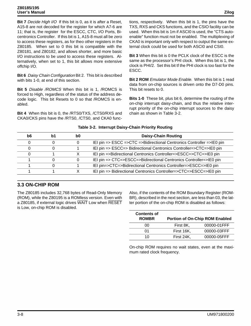
Figure 3-15 shows the timing for exiting SLEEP Mode dueto an interrupt request. Note that the Z80185 takes about1.5 clocks to restart.
Figure 3-14. HALT Timing
HALT Op-code Fetch Cycle HALT Mode
φT2 T3 T1 T2 T3 T1 T2
INTi, NMI
A0-A19
HALT
M1
MREQ
RD
InterruptAcknowledge Cycle
HALT Op-code Address HALT Op-code Address + 1
Z80185/195Zilog User’s Manual
UM971800200 3-13
3
3.6.4 IOSTOP ModeIOSTOP Mode is entered by setting the IOSTOP bit of theI/O Control Register (ICR) to 1. In this case, on-chip I/O(ASCI, CSI/O, PRt) stops operating but the CPU continuesto operate. Recovery from IOSTOP Mode is by resettingthe IOSTOP bit in ICR to 0.
3.6.5 SYSTEM STOP ModeSYSTEM STOP Mode is the combination of SLEEP andIOSTOP Modes. SYSTEM STOP Mode is entered by set-ting the IOSTOP bit in ICR to 1 followed by execution of theSLP instruction. In this Mode, on-chip I/O and CPU stopoperating , reducing power consumption, but the PHI out-put continues to operate. Recovery from SYSTEM STOPMode is the same as recovery from SLEEP Mode exceptthat internal I/O sources (disabled by IOSTOP) cannotgenerate a recovery interrupt.
3.6.6 IDLE ModeSoftware can put the Z80185 into this Mode by setting theIOSTOP bit (ICR5) to 1, CCR6 to 0, CCR3 to 1 and exe-cuting the SLP instruction. The oscillator keeps operatingbut its output is blocked to all circuitry including the PHIpin. DRAM refresh and all internal devices stop, but exter-nal interrupts can occur. Bus granting to external masterscan occur if the BREXT bit in the CPU control Register(CCR5) was set to 1 before Idle Mode was entered.
The Z80185 leaves Idle Mode in response to a low on RE-SET, an external interrupt request on NMI, or an externalinterrupt request on INT0, INT1 or INT2 that is enabled inthe INT/TRAP Control Register. As described above forSLEEP Mode, when the Z80185 leaves Idle Mode due toan NMI, or due to an enabled external interrupt requestwhen the IEF flag is 1 due to an EI instruction, it starts byperforming the interrupt with the return address being thatof the instruction after the SLP instruction.
Figure 3-15. SLEEP Timing
SLP 2nd Op-codeSLEEP Mode
φT2 T3 T1 T2 TS TS T1
INTi, NMI
A0-A19
HALT
M1
Op-code Fetch or InterruptAcknowledge Cycle
SLP 2nd Op-code Address FFFFFH
Fetch Cycle
T2 T3

Z80185/195User’s Manual Zilog
3-14 UM971800200
3.6 HALT AND LOW-POWER OPERATING MODES (Continued)
If the Z80185 leaves Idle Mode due to an external interruptrequest that's enabled in the INT/TRAP Control Registerbut the IEF1 bit is 0 due to a DI instruction, the processorrestarts by executing the instruction(s) following the SLPinstruction.
Figure 3-17 shows the timing for exiting Idle Mode due toan interrupt request. Note that the Z80185 takes about 9.5clocks to restart.
Figure 3-16. Z80185/195 IDLE Mode Exit due to External Interrupt
φT1 T2 T4
NMI
A19-A0
HALT
M1
Op-code Fetch or InterruptAcknowledge Cycle
FFFFFH
Idle Mode
T3
9.5 Cycle Delay from INTi Asserted
INTi
or

Z80185/195Zilog User’s Manual
UM971800200 3-15
3
While the Z80185 is in Idle Mode, it will grant the bus to anexternal master if the BREXT bit (CCR5) is 1. Figure 3-18shows the timing for this sequence. Note that the part
takes 8 clock cycles longer to respond to the Bus Requestthan in normal operation.
After the external master negates the Bus Request, theZ80185 disables the PHI clock and remains in IDLE Mode.
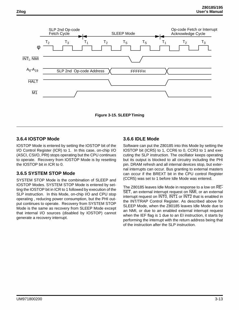
3.6.7 STANDBY Mode (With or without Quick Recovery)Software can put the Z80185 into this Mode by setting theIOSTOP bit (ICR5) to 1 and CCR6 to 1, and executing theSLP instruction. This Mode stops the on-chip oscillator andthus draws the least power of any Mode, less than 10 µA.
As with Idle Mode, the Z80185 will leave Standby Mode inresponse to a Low on RESET or on NMI, or a low on INT0-2 that is enabled by a 1 in the corresponding bit in theINT/TRAP Control Register, and will grant the bus to anexternal master if the BREXT bit in the CPU Control Reg-ister (CCR5) is 1. But the time required to restart is greatlyincreased by the need to restart the on-chip oscillator andensure that it has stabilized to square-wave operation.
When an external clock is connected to the EXTAL pinrather than a crystal to the XTAL and EXTAL pins, and theexternal clock runs continuously, there is little need to useSTANDBY Mode because there is no time required to re-start the oscillator, and other Modes restart faster. Howev-
er, if external logic stops the clock during Standby Mode(e.g., by decoding HALT low and M1 high for several clockcycles), then standby Mode can be useful to allow the ex-ternal clock source to stabilize after it is re-enabled.
When external logic drives RESET low to being a Z80185out of Standby Mode, and a crystal is used or an externalclock source has been stopped, the external logic musthold RESET Low until the on-chip oscillator or externalclock source has restarted and stabilized.
The clock stability requirements of the Z80185 are muchless in the 'divide by two' Mode that's selected by a Resetsequence and thereafter controlled by the Clock Divide bitin the CPU Control Register (CCR7). Because of this, soft-ware should:
a. Program CCR7 to 0 to select "divide by two" Mode, be-fore the SLP instruction that enters Standby Mode,and,
Figure 3-17. Bus Granting to External Master in Idle Mode
φTX
BUSREQ
A19-A0
HALT
M1
Bus Release Mode Idle Mode
FFFFFH
Idle Mode
9.5 Cycle Delay until BUSACK Asserted
BUSACK
TX
High ImpedanceFFFFFH
High
Low
Z80185/195User’s Manual Zilog
3-16 UM971800200
3.6 HALT AND LOW-POWER OPERATING MODES (Continued)
b. After a Reset, interrupt or in-line restart after the SLP01 instruction, delay programming CCR7 back to 1 toset "divide by one" Mode, as long as possible to allowadditional clock stabilization time.
When software program CCR6 to 1 before a SLP instruc-tion that enters Standby Mode, the value that it writes tothe CCR3 bit determines how long the Z80185 will wait foroscillator restart and stabilization, when it leaves standbyMode because of anóexternal interrupt request. If CCR3 is0, the Z80185 waits 217 (131,072) clock cycles, while ifCCR3 is 1, it waits only 64 clock cycles. The latter is called"Quick Recovery" Mode. The same delay applies to grant-ing the bus to an external master during Standby Mode,when the BREXT bit in the CPU Control Register (CCR5)is 1.
As described previously for Sleep and Idle Modes, when aZ801x5 leaves standby Mode due to NMI Low, or when itleaves Standby Mode due to an enabled INT0-2 low whenthe IEF1 flag is 1 due to an IE instruction, it starts by per-forming the interrupt with the return address being that ofthe instruction following the SLP instruction. If the Z80185leaves Standby Mode due to an external interrupt requestthat's enabled in the INT/TRAP Control Register, but theIEF, bit is 0 due to a DI instruction, the processor restartsby executing the instruction(s) following the SLP instruc-tion. If INT0, or INT1 or INT2 goes inactive before the endof the clock stabilization delay, the Z80185 stays in Stand-by Mode.
Figure 3-19 shows the timing for leaving Standby Modedue to an interrupt request. Note that the Z80185 takes ei-ther 64 or 217 (131,072) clocks to restart, depending on theCCR3 bit.
Figure 3-18. Z8S180/Z8L180 STANDBY Mode Exit due to External Interrupt
φT1 T2 T4
NMI
A19-A0
HALT
M1
Op-code Fetch or InterruptAcknowledge Cycle
FFFFFH
Standby Mode
T3
217 or 64 Cycle Delay from INTi Asserted
INTi
or

Z80185/195Zilog User’s Manual
UM971800200 3-17
3
While the Z801x5 is in Standby Mode, it will grant the busto an external master if the BREXT bit (CCR5) is 1. Figure3-20 shows the timing of this sequence. Note that the parttakes 64 or 217 (131,072) clock cycles to grant the bus de-pending on the CCR3 bit.
The latter (non-Quick-Recovery) case may be prohibitivefor many "demand driven" external masters. If so, QuickRecovery or Idle Mode can be used.
3.7 TRAPS AND INTERRUPTS
The Z80185 has 12 priority levels for interrupts. As shownin Figure 3-21, eight of them are assigned to specific on-chip sources. Three levels are assigned to the NMI, INT1and INT2 pins, each of which can be connected to a spe-cific external interrupt source or shared among multiplesources. In the latter case, identification of the source ofan interrupt is left to software polling.
The twelfth interrupt level is shared among several on-chipinterrupt sources (the ESCC, CTCs, and the BidirectionalCentronics controller) and the INT0 pin. INT0 can be con-nected to a specific external interrupt source or sharedamong multiple sources. The on-chip logic associated withthis interrupt level allows for the automatic identification ofthe highest priority interrupting device within the level, bymeans of an interrupt acknowledge daisy chain.
Figure 3-19. Bus Granting to External Master During Standby Mode
φTX TX
BUSREQ
A19-A0
HALT
M1
Standby ModeBus Release Mode
FFFFFH
Standby Mode
64 or 217 Cycle Delay after BUSREQ Asserted
BUSACK
FFFFFH
Low
High

Z80185/195User’s Manual Zilog
3-18 UM971800200
3.7 TRAPS AND INTERRUPTS (Continued)
3.7.1 INT/TRAP Control Register (ITC, I/O Address 34H)This register as seen in Figure 3-21 is used in handlingTRAP interrupts and to enable or disable Maskable Inter-rupt Level 0 and the INT1 and INT2 pins.
TRAP (bit 7). This bit is set to 1 when an undefined op-code is fetched. TRAP can be reset under program controlby writing it with a 0, however, it cannot be written with 1under program control. TRAP is reset to 0 during RESET.
UFO: Undefined Fetch Object (bit 6). When a TRAP in-terrupt occurs the contents of UFO allow determination ofthe starting address of the undefined instruction. This isnecessary since the TRAP may occur on either the secondor third byte of the op-code. UFO allows the stacked PCvalue to be correctly adjusted. If UFO = 0, the first op-codeis at the stacked PC-1. If UFO = 1, the first op-code ad-dress is the stacked PC-2. UFO is Read-Only.
ITE2, 1, 0: Interrupt Enable 2, 1, 0 (bits 2-0). ITE2 andITE1, enable and disable the external interrupt inputs/INT2 and /INT1, respectively. ITE0 enables and disablesinterrupts from the on-chip ESCC, CTCs and BidirectionalCentronics controller as well as the external interrupt input
/INT0. A 1 in a bit enables the corresponding interrupt levelwhile a 0 disables it. A Reset sets ITE0 to 1 and clearsITE1 and ITE2 to 0.
TRAP Interrupt. The Z80180 generates a non-maskable(not affected by the state of IEF1) TRAP interrupt when anundefined op-code fetch occurs. This feature can be usedto increase software reliability, implement an "extended"instruction set, or both. TRAP may occur during op-codefetch cycles and also if an undefined op-code is fetchedduring the interrupt acknowledge cycle for INT0 whenMode 0 is used.
When a TRAP interrupt occurs, the Z80185/195 operatesas follows:
1. The TRAP bit in the Interrupt TRAP/Control (ITC)register is set to 1.
2. The current PC (Program Counter) value, reflectingthe location of the undefined op-code, is saved on thestack.
3. The Z80180 restarts execution at logical address 0.Note that if logical address 0000H is mapped tophysical address 00000H, the vector is the same asfor RESET. In this case, testing the TRAP bit in ITC willreveal whether the restart at physical address 00000Hwas caused by RESET or TRAP.
TRAP interrupts occur after fetching an undefined secondop-code byte following one of the "prefix" op-codes CBH,DDH, EDH, or FDH, or after fetching an undefined third op-code byte following one of the "double prefix" op-codes
Figure 3-20. Interrupt Levels
HigherPriority
LowerPriority
(1) TRAP (Undefined Op-code Trap(2) NMI (Non-Maskable Interrupt)(3) INT0 (Maskable Interrupt Level 0)(4) INT1 (Maskable Interrupt Level 1) (5) INT2 (Maskable Interrupt Level 2)(6) Timer0(7) Timer1(8) DMA Channel 0(9) DMA Channel 1(10) Clocked Serial I/O Port(11) Asynchronous SCI Channel 0(12) Asynchronous SCI Channel 1
InternalExternalInternal and External
External
Internal
Figure 3-21. Int/Trap Control Register
Bit
TRAP UFO
R/W R/W R/W
––
7 6 5 4 3 2 1 0
–– –– ITE2 ITE1 ITE0
R/W R
Z80185/195Zilog User’s Manual
UM971800200 3-19
3
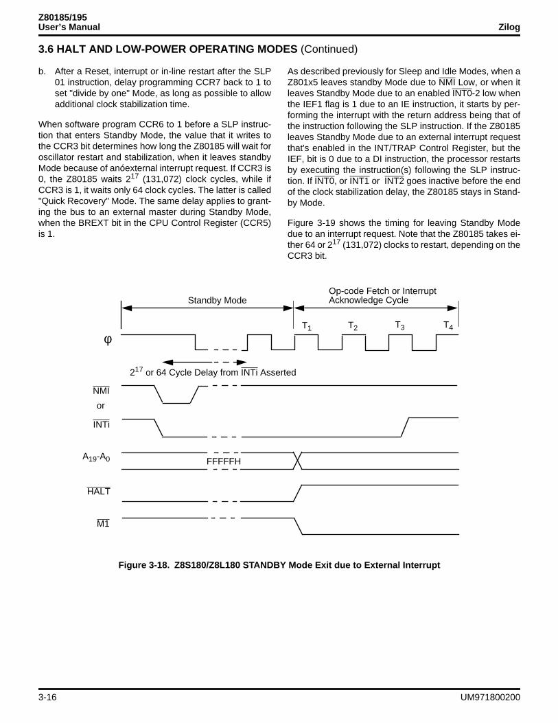
DDCBH or FDCBH. Figures 3-21 and 3-22 show the tim-ing for the two cases of TRAP interrupts.
The state of the UFO (Undefined Fetch Object) bit in ITCallows TRAP software to correctly "adjust" the stacked PC,
depending on whether the second or third byte of the op-code generated the TRAP. If UFO=0, the starting addressof the invalid instruction is equal to the stacked PC-1. IfUFO=1, the starting address of the invalid instruction isequal to the stacked PC-2.
Figure 3-22. TRAP Timing-2nd Op-code Undefined
T1 T2 T3 TTP Ti Ti Ti Ti Ti T1 T2 T3 T2 T3 T1T1 T2
A0-A18 (A19)
φ
D0-D7
PC 0000HSP-1
Undefined
MREQ
M1
RD
WR
T3
SP-2
Op-code
PCH PCL
2nd Op-codeFetch Cycle
PC StackingOp-codeFetch Cycle
Restart from 0000H

Z80185/195User’s Manual Zilog
3-20 UM971800200
3.7 TRAPS AND INTERRUPTS (Continued)
3.7.2 Interrupt Enabling and DisablingAll of the interrupt levels except TRAP and NMI are subjectto "global" enabling and disabling by means of the EI andDI instructions which control two internal bits called IEF1and IEF2.
IEF1 controls the overall enabling and disabling of all inter-nal and external maskable interrupts (in other words, all in-terrupts except NMI and TRAP).
If IEF1 = 0, all maskable interrupts are disabled. IEF1 canbe reset to 0 by the DI (Disable Interrupts) instruction andset to 1 by the EI (Enable Interrupts) instruction.
The purpose of IEF2 is to correctly manage the occurrenceof NMI. During NMI, the prior state is saved by copying thestate of IEF1 into IEF2 and maskable interrupts are thendisabled by clearing IEF1 to 0.
At the end of the NMI interrupt service routine, executionof the RETN (Return from Non-maskable interrupt) will au-tomatically restore the interrupt receiving state (by copyingIEF2 to IEF1) prior to the occurrence of NMI.
The state of IEF2 can be copied to the P/V bit of the CPUStatus Register by executing an LD A, I or LD A, R instruc-tion.
Table 3-4 summarizes the relationship between variousoperations and the IEF1 and IEF2 flags.
Figure 3-23. TRAP Timing-3rd Op-code Undefined
T1 T2 T3 T1 T2 TTP T3 Ti Ti T1 T2 T3 T2 T3 T1T1 T2
A0-A18 (A19)
φ
D0-D7
PC 0000HSP-1
Undefined
MREQ
M1
RD
WR
T3
SP-2
Op-code
PC-1H PC-1L
3nd Op-codeFetch Cycle PC Stacking
Op-codeFetch Cycle
Restart
Memory
IX + d, IY + d
Ti Ti
Read Cycle
from 0000H

Z80185/195Zilog User’s Manual
UM971800200 3-21
3
In addition to the global interrupt enabling and disabling af-forded by the EI and DI instructions and the IEF1 and IEF2bits, each interrupt source in the Z80185 (other than TRAPand NMI) has its own individual enabling/disabling mecha-nism which is described in later sections.
3.7.3 NMI - Non-Maskable InterruptThe NMI interrupt input is edge sensitive and cannot bemasked by software. When NMI is detected, the Z80180operates as follows.
1. DMAC operation is suspended by clearing the DME(DMA Main Enable) bit in DCNTL.
2. The PC is pushed onto the stack.
3. The contents of IEF1 are copied to IEF2. This savesthe interrupt reception state that existed prior to NMI.
4. IEF1 is cleared to 0. This disables all external andinternal maskable interrupts (in other words, allinterrupts except NMI and TRAP).
5. Execution commences at logical address 0066H.
The RETN instruction provides a convenient way to returnfrom a non-maskable interrupt if the software has not doneany EI or DI instructions since the NMI occurred. It copiesthe saved state of IEF2 to IEF1 and restores the return ad-dress from the stack.
Alternatively, the NMI software can sense the state of IEF2by performing an LD A,I or LD A,R instruction, which cop-ies IEF2 to the P/V flag, branching on P/V, and setting astatus bit in memory accordingly. The software can then doEI and DI instructions as needed. When it is time to returnfrom the NMI, the software can test the status bit in mem-ory and use either an IE-RET or DI-RET sequence to re-turn to the interrupted process.
An NMI service routine can protect against multiple edgeson the /NMI line (e.g., contact bounce on a push-button) bymaintaining an "in NMI" status bit in memory. One of thefirst things the service routine should do is to test this sta-tus bit, and do an immediate RETN if the bit is set. If not, itshould set the bit. When it is time to return from the NMI,the software should clear the bit.
Table 3-3. Operations Affecting or Using IEF1 and IEF2
CPU Operation IEF1 IEF2 Remarks
RESET 0 0 Inhibits all interrupts except NMI and TRAPNMI 0 IEF1 Copies the contents of IEF1 to IEF2.
RETN IEF2 Not Affected
Interrupt Except NMI and TRAP 0 0 Inhibits all interrupts except NMI and TRAP.RETI Not Affected Not AffectedTRAP Not Affected Not AffectedEI 1 1DI 0 0LD A, I Not Affected Not Affected Copies the contents of IEF2 to the P/V flag.
LD A, R Not Affected Not Affected Copies the contents of IEF2 to the P/V flag.

Z80185/195User’s Manual Zilog
3-22 UM971800200
3.7 TRAPS AND INTERRUPTS (Continued)
Figure 3-24 shows the timing of a Non-Maskable Interrupt./NMI is edge sensitive – a falling edge sets an internallatch that remains set until the interrupt occurs. This latchis sampled by the falling edge of PHI in the second-last
clock cycle of each instruction. If the latch has been set bythe time of that falling edge, the non-maskable interrupt oc-curs at the end of the instruction.
3.7.4 Maskable Interrupt Level 0 This is the next highest priority interrupt level after NMI andis shared by the on-chip ESCC, CTCs, Bidirectional Cen-tronics interface, and the INT0 pin. The logical OR (posi-tive logic AND) of these four requests is sampled at thefalling edge of PHI in the second-last clock cycle of the ex-ecution of most instructions. (Certain instructions such asEI do not allow an interrupt after them.) If the composite re-quest is Low at such a falling edge, and the ITE0 bit in theINT/TRAP Control Register (ITC0) is 1, and the IEF, bit is1 (due to an EI instruction) then the Z80185 performs aninterrupt after the instruction.
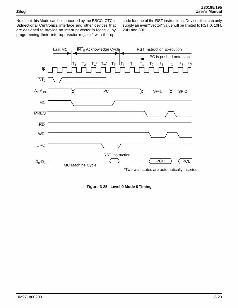
The type of interrupt processing the Z80185 performs foran interrupt at this level is controlled by the Interrupt Mode(IM) instruction. There are three cases called Modes 0, 1,and 2.
Level 0 Mode 0 Interrupts. After a Reset and/or an IM 0instruction, the Z80185 begins an interrupt sequence byclearing the IEF1 and IEF2 bits to disable further interrupts,and fetching an op-code byte from the D7-0 lines using aspecial cycle in which it drives M1 and IORQ both Low, asshown in Figure 3-25.
Often this instruction is one of the eight single-byte RST(Restart) instructions which stack the PC and restart exe-cution at one of the fixed logical addresses 0, 8, ..., 38H.However, multibyte instructions can be processed if thedevice providing the instruction can provide such a multi-byte sequence. Unlike all other interrupts, the Z801x5does not automatically stack the PC in this Mode.
A TRAP interrupt will occur if an invalid multibyte instruc-tion is provided in this Mode.
Figure 3-24. NMI Timing
T1 T2 T3 Ti Ti T1 T2 T3 T1 T1 T2 T3
NMI
φ
A0-A19 PC 0066HSP-1
MREQ
M1
RD
WR
SP-2
Last MC
PC is pushed onto stack
Op-code Fetch
Restart from 0066H
NMI Acknowledge Cycle
T2 T3
D0-D7 PCH PCHInstruction
Z80185/195Zilog User’s Manual
UM971800200 3-23
3
Note that this Mode can be supported by the ESCC, CTCs,Bidirectional Centronics interface and other devices thatare designed to provide an interrupt vector in Mode 2, byprogramming their "interrupt vector register" with the op-
code for one of the RST instructions. Devices that can onlysupply an even" vector" value will be limited to RST 0, 10H,20H and 30H.
Figure 3-25. Level 0 Mode 0 Timing
T1 T2 Tw* Tw* T3 Ti Ti T1 T2 T2 T3
INT0
φ
A0-A19 PC SP-1
MREQ
M1
RD
WR
SP-2
Last MC
PC is pushed onto stack
RST Instruction ExecutionINT0 Acknowledge Cycle
T3 T1
IORQ
RST Instruction
PCH PCLMC Machine Cycle
D0-D7
*Two wait states are automatically inserted.

Z80185/195User’s Manual Zilog
3-24 UM971800200
3.7 TRAPS AND INTERRUPTS (Continued)
Level 0 Mode 1 Interrupts. After an IM 1 instruction, theZ80185 performs a Level 0 interrupt by clearing IEF1 andIEF2, stacking the PC, and beginning execution at logical
address 0038H. In effect this is like a Level 0 Mode 0 inter-rupt, in which the responding device provides an RST 38Hinstruction (FFH) see Figure 3-26.
Before describing Level 0 Mode 2 it will be helpful to de-scribe the I register.
The I Register and LD A<->I instructions. The Z80185includes an internal I register that is used during Level 0Mode 2 interrupts, INT1 and INT2 interrupts and interruptsfrom the on-chip DMAs, ASCIs, PRTs and CSI/0. Ratherthan having an address in I/O space like most registers inthe Z80185, the I register is loaded by the special instruc-tion LD I, A, and can be read back by the LD A, I instruc-tion.
During the interrupts noted above, the Z80185 places thecontents of I on the A15-8 lines while it fetches a two-bytestarting address of the interrupt service routine from mem-ory.
Level 0 Mode 2 Interrupts. After an IM 2 instruction, theZ801x5 starts a Level 0 interrupt by clearing the IEF1 andIEF2 bits to disable further maskable interrupts and per-forming a special interrupt acknowledge cycle in which itdrives M1 and IORQ both Low, as shown in Figure 3-27.
Figure 3-26. Level 0 Mode 1 Timing
T1 T2 Tw* Tw* T3 T1 T2 T3 T1 T1 T2
INT0
φ
A0-A19 PC SP-1
MREQ
M1
RD
WR
SP-2
Last MC
PC is pushed onto stack
Op-code Fetch CycleINT0 Acknowledge Cycle
T2 T3
PCHD0-D7
*Two wait states are automatically inserted.
T3
0038H
IORQ
PCL
ST

Z80185/195Zilog User’s Manual
UM971800200 3-25
3
Through this point, operation is as in Mode 0. But ratherthan treating the byte supplied by the interrupting deviceas an instruction op-code as in Mode 0, in Mode 2 theZ80185 treats the value from the device as an "interruptvector." It automatically stacks the return address from PC,and thereafter fetches two bytes from memory. It fetchesthe first byte from the logical address formed by using thecontents of the I register as the MS byte (A15-8) and the"vector" value obtained from the device as the LS byte (A7-0). It treats this first byte as the LS byte of the starting ad-dress of the interrupt service routine (ISR). It then fetchesa second byte from the next higher address, which it treatsas the MS byte of the starting address of the ISR. Finally,it begins executing the instruction(s) at the address it hasfetched from memory.
Figure 3-28 depicts the process of fetching the vector forLevel 0 Mode 2 Interrupts.
Figure 3-27. Level 0 Interrupt Mode 2 Timing
T1 T2 Tw* Tw* T3 Ti T1 T2 T3 T3 T1
INT0
φ
A0-A19 PC SP-1
MREQ
M1
RD
WR
SP-2
Last MC
PC is pushed
Op-codeAcknowledge Cycle
T1 T2
PCHD0-D7
*Two wait states are automatically inserted.
T2
Vector
IORQ
PCL
ST
T3T1 T2 T3T1 T2T3
Vector Lower
Vector + 1Starting Address
Starting Address(lower address)
Starting Address(upper address)Lower Vector
Fetch Cycle
InterruptAddress Read onto stack Manipulation Cycle

Z80185/195User’s Manual Zilog
3-26 UM971800200
3.7 TRAPS AND INTERRUPTS (Continued)
3.7.5 Interrupt Vector Low (IL) RegistersBits 7-5 of IL are used as bits 7-5 of the synthesized inter-rupt vector during interrupts for the INT1 and INT2 pins
and for the DMAs, ASCIs, PRTs, and CSI/O. These threebits are cleared to 0 during Reset (Figure 3-29).
Figure 3-28. Level 0 Mode 2 Vector Acquisition
16-Bit Vector
Interrupt VectorRegister 1
8-Bit onData Bus
Low-order 8 Bitsof Starting Address
High-order 8 Bitsof Starting Address
Memory
Vector + 1
Vector
256-ByteVector Table
Figure 3-29. Interrupt Vector Low Register (IL: I/O Address = 33H)
Bit
IL 7 IL 6
Interrupt Source Dependent Code
IL 5
7 6 5 4 3 2 1 0
–– ––
R/W R/W
–– –– ––
R/W
Programmable
Z80185/195Zilog User’s Manual
UM971800200 3-27
3
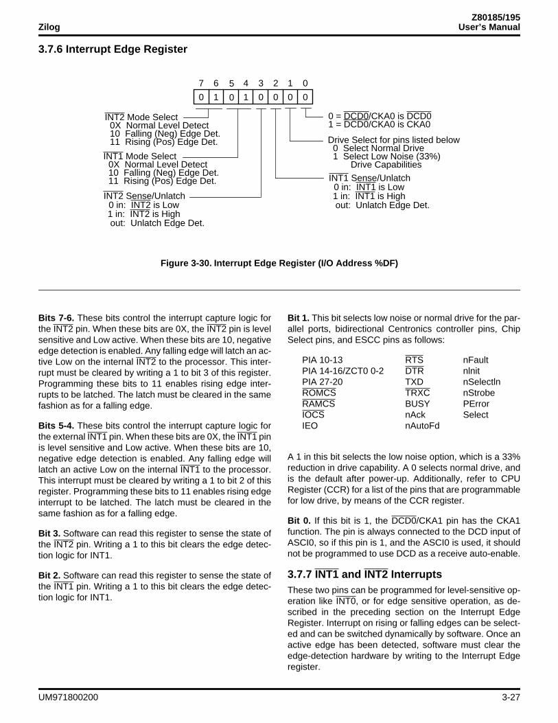
3.7.6 Interrupt Edge Register
Bits 7-6. These bits control the interrupt capture logic forthe INT2 pin. When these bits are 0X, the INT2 pin is levelsensitive and Low active. When these bits are 10, negativeedge detection is enabled. Any falling edge will latch an ac-tive Low on the internal INT2 to the processor. This inter-rupt must be cleared by writing a 1 to bit 3 of this register.Programming these bits to 11 enables rising edge inter-rupts to be latched. The latch must be cleared in the samefashion as for a falling edge.
Bits 5-4. These bits control the interrupt capture logic forthe external INT1 pin. When these bits are 0X, the INT1 pinis level sensitive and Low active. When these bits are 10,negative edge detection is enabled. Any falling edge willlatch an active Low on the internal INT1 to the processor.This interrupt must be cleared by writing a 1 to bit 2 of thisregister. Programming these bits to 11 enables rising edgeinterrupt to be latched. The latch must be cleared in thesame fashion as for a falling edge.
Bit 3. Software can read this register to sense the state ofthe INT2 pin. Writing a 1 to this bit clears the edge detec-tion logic for INT1.
Bit 2. Software can read this register to sense the state ofthe INT1 pin. Writing a 1 to this bit clears the edge detec-tion logic for INT1.
Bit 1. This bit selects low noise or normal drive for the par-allel ports, bidirectional Centronics controller pins, ChipSelect pins, and ESCC pins as follows:
PIA 10-13 RTS nFaultPIA 14-16/ZCT0 0-2 DTR nlnitPIA 27-20 TXD nSelectlnROMCS TRXC nStrobeRAMCS BUSY PErrorIOCS nAck SelectIEO nAutoFd
A 1 in this bit selects the low noise option, which is a 33%reduction in drive capability. A 0 selects normal drive, andis the default after power-up. Additionally, refer to CPURegister (CCR) for a list of the pins that are programmablefor low drive, by means of the CCR register.
Bit 0. If this bit is 1, the DCD0/CKA1 pin has the CKA1function. The pin is always connected to the DCD input ofASCI0, so if this pin is 1, and the ASCI0 is used, it shouldnot be programmed to use DCD as a receive auto-enable.
3.7.7 INT1 and INT2 Interrupts These two pins can be programmed for level-sensitive op-eration like INT0, or for edge sensitive operation, as de-scribed in the preceding section on the Interrupt EdgeRegister. Interrupt on rising or falling edges can be select-ed and can be switched dynamically by software. Once anactive edge has been detected, software must clear theedge-detection hardware by writing to the Interrupt Edgeregister.
Figure 3-30. Interrupt Edge Register (I/O Address %DF)
0
0 = DCD0/CKA0 is DCD0INT2 Mode Select
7
1
6
0
5
1
4
0
3
0
2
0
1
0
0
0X Normal Level Detect 10 Falling (Neg) Edge Det. 11 Rising (Pos) Edge Det.
INT1 Mode Select 0X Normal Level Detect 10 Falling (Neg) Edge Det. 11 Rising (Pos) Edge Det.
INT2 Sense/Unlatch 0 in: INT2 is Low1 in: INT2 is High out: Unlatch Edge Det.
INT1 Sense/Unlatch 0 in: INT1 is Low1 in: INT1 is High out: Unlatch Edge Det.
1 = DCD0/CKA0 is CKA0
Drive Select for pins listed below 0 Select Normal Drive 1 Select Low Noise (33%) Drive Capabilities
Z80185/195User’s Manual Zilog
3-28 UM971800200
3.7 TRAPS AND INTERRUPTS (Continued)
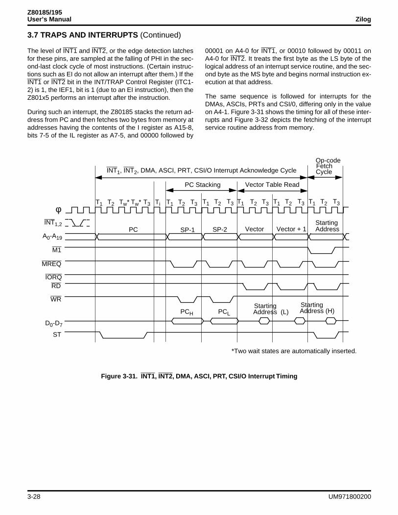
The level of INT1 and INT2, or the edge detection latchesfor these pins, are sampled at the falling of PHI in the sec-ond-last clock cycle of most instructions. (Certain instruc-tions such as EI do not allow an interrupt after them.) If theINT1 or INT2 bit in the INT/TRAP Control Register (ITC1-2) is 1, the IEF1, bit is 1 (due to an EI instruction), then theZ801x5 performs an interrupt after the instruction.
During such an interrupt, the Z80185 stacks the return ad-dress from PC and then fetches two bytes from memory ataddresses having the contents of the I register as A15-8,bits 7-5 of the IL register as A7-5, and 00000 followed by
00001 on A4-0 for INT1, or 00010 followed by 00011 onA4-0 for INT2. It treats the first byte as the LS byte of thelogical address of an interrupt service routine, and the sec-ond byte as the MS byte and begins normal instruction ex-ecution at that address.
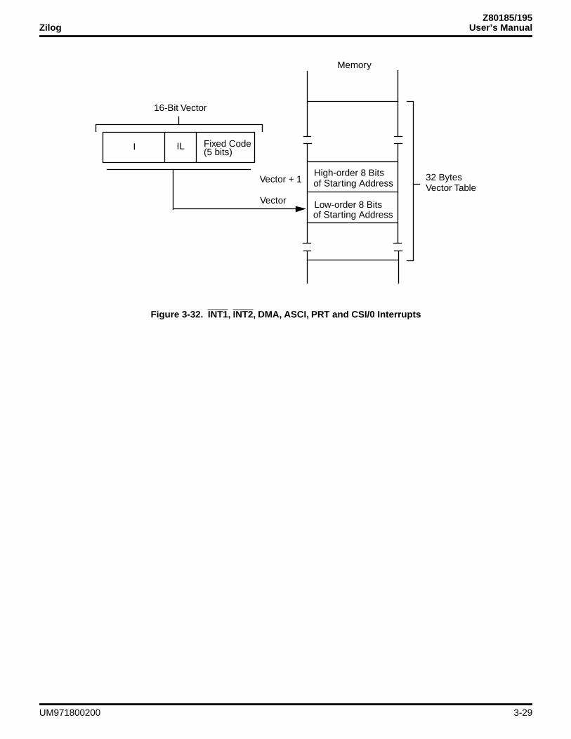
The same sequence is followed for interrupts for theDMAs, ASCIs, PRTs and CSI/0, differing only in the valueon A4-1. Figure 3-31 shows the timing for all of these inter-rupts and Figure 3-32 depicts the fetching of the interruptservice routine address from memory.
Figure 3-31. INT1, INT2, DMA, ASCI, PRT, CSI/O Interrupt Timing
T1 T2 Tw* Tw* T3 Ti T1 T2 T3 T3 T1
INT1,2
φ
A0-A19
PC SP-1
MREQ
M1
RD
WR
SP-2
PC Stacking
Op-code
INT1, INT2, DMA, ASCI, PRT, CSI/O Interrupt Acknowledge Cycle
T1 T2
PCH
D0-D7
*Two wait states are automatically inserted.
T2
Vector
IORQ
PCL
ST
T3T1 T2 T3T1 T2T3
Vector + 1Starting
Starting Starting
Fetch
Vector Table Read
Address
Cycle
Address (L) Address (H)
Z80185/195Zilog User’s Manual
UM971800200 3-29
3
Figure 3-32. INT1, INT2, DMA, ASCI, PRT and CSI/0 Interrupts
16-Bit Vector
I Fixed CodeIL
Low-order 8 Bitsof Starting Address
High-order 8 Bitsof Starting Address
Memory
Vector + 1
Vector
32 BytesVector Table
(5 bits)
Z80185/195User’s Manual Zilog
3-30 UM971800200
3.7.8 DMA, ASCI, PRT and CSI/0 Interrupts Each of these devices includes one or more interrupt con-ditions or sources which can be individually enabled orarmed to interrupt the Z80185 as described in the latersections about these devices. The processor samples "en-abled request" signals from each device, at the fallingedge of PHI in the second-last clock cycle of most instruc-tions. (Certain instructions such as EI do not permit inter-rupts after them.) If an "enable request" line is sampled as
"asserted," and the IEF, bit is 1 (due to an EI instruction),then the Z80185 performs an interrupt after the instruction.
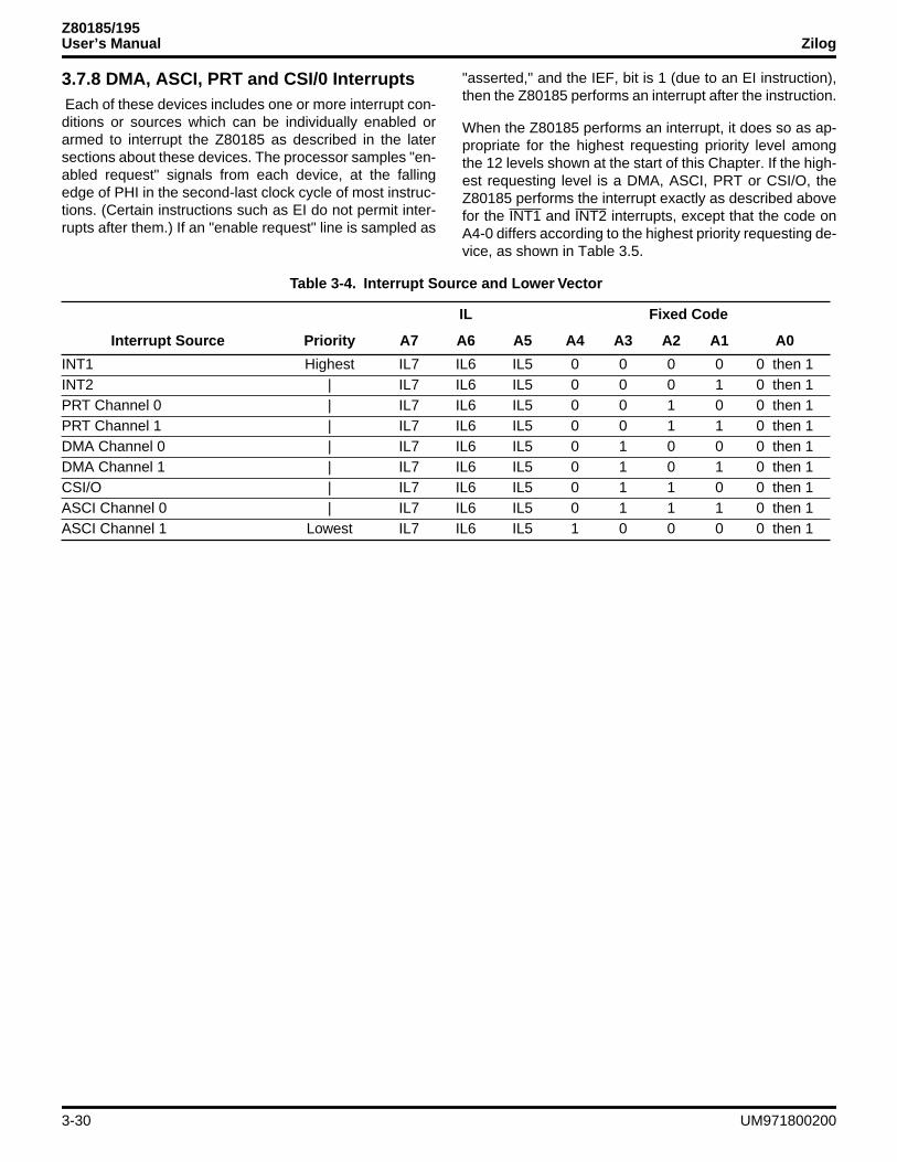
When the Z80185 performs an interrupt, it does so as ap-propriate for the highest requesting priority level amongthe 12 levels shown at the start of this Chapter. If the high-est requesting level is a DMA, ASCI, PRT or CSI/O, theZ80185 performs the interrupt exactly as described abovefor the INT1 and INT2 interrupts, except that the code onA4-0 differs according to the highest priority requesting de-vice, as shown in Table 3.5.
Table 3-4. Interrupt Source and Lower Vector
IL Fixed Code
Interrupt Source Priority A7 A6 A5 A4 A3 A2 A1 A0
INT1 Highest IL7 IL6 IL5 0 0 0 0 0 then 1INT2 | IL7 IL6 IL5 0 0 0 1 0 then 1PRT Channel 0 | IL7 IL6 IL5 0 0 1 0 0 then 1PRT Channel 1 | IL7 IL6 IL5 0 0 1 1 0 then 1DMA Channel 0 | IL7 IL6 IL5 0 1 0 0 0 then 1DMA Channel 1 | IL7 IL6 IL5 0 1 0 1 0 then 1CSI/O | IL7 IL6 IL5 0 1 1 0 0 then 1ASCI Channel 0 | IL7 IL6 IL5 0 1 1 1 0 then 1ASCI Channel 1 Lowest IL7 IL6 IL5 1 0 0 0 0 then 1

Z80185/195Zilog User’s Manual
UM971800200 3-31
3
The interrupt service routine for one of these devicesshould take appropriate action for the current conditions,including register accesses to the device that will typicallycause it to negate its "enabled request" signal, before re-enabling interrupts and returning to the interrupted pro-cess. These actions and register accesses are describedlater, in the sections about the devices.
3.7.9 The RETI Instruction The original Zilog Z80 peripheral chips (PIO, SIO, CTCand DMA) include a special circuit that monitors the in-struction stream being fetched by the Z80 processor andrecognizes the special instruction RETI. To the processor,RETI operates exactly like RET, but to Z80 peripherals, ithas the additional meaning that a peripheral that has its In-terrupt Under Service (IUS) bit set and its IEI input assert-ed, should clear its IUS bit because its interrupt serviceroutine is now concluded.
The CTCs in the Z80185 are compatible with the originalZ80-CTC and interrupt service routines for the CTCsshould end with RETI instructions, as should ISRs for anyexternal Z80-PIO, SIO, CTC or DMA. In ISRs for other on-
chip or external devices, RETI is no different from RET andthe latter is preferred because it is shorter and faster. Notethat RETI does not re-enable interrupts and must be pre-ceded by an EI instruction just like RET.
The IUS mechanism is intended to allow "nested" inter-rupts, wherein a higher priority device can interrupt the in-terrupt service routine for a lower priority device, the prior-ity being determined by the IEO-IEI daisy chain. Morerecent daisy-chainable devices like the ESCC and Bidirec-tional Centronics controller include explicit means to cleartheir IUS bits and do not recognize RETI. Non-daisy-chain-able devices like the DMAs, ASCIs, PRTs and CSI/O donot support nested interrupts at all and interrupt serviceroutines for such devices typically run to completion with-out being interrupted, because they end with an EI directlyfollowed by an RET instruction.
The Z80185 processor performs an RETI instruction in twodifferent ways depending on the MIE bit in the OperatingMode Control Register (OMCR7) as described in the ear-lier section "Z80 versus 64180 Compatibility."
3.8 MEMORY MANAGEMENT UNIT (MMU)
The Z80185/195 includes an on-chip MMU which performsthe translation of the CPU 64 KB (16-bit addresses 0000Hto FFFFH) logical memory address space into a 1024 KB(20-bit addresses 00000H to FFFFFH) physical memoryaddress space. Address translation occurs internally inparallel with other CPU operation.
Logical Address Spaces. The 64 KB CPU logical ad-dress space is interpreted by the MMU as consisting of up
to three separate logical address areas, Common Area 0,Bank Area, and Common Area 1.
As shown in Figure 3-33, a variety of logical memory con-figurations are possible. The boundaries between theCommon and Bank Areas can be programmed with 4 KBresolution.
Figure 3-33. Logical Address Mapping Examples
Common Area 1 Common Area 1 Common Area 1 Common Area 1
Bank Area
Common Area 0Bank Area Common Area 0

Z80185/195User’s Manual Zilog
3-32 UM971800200
3.8 MEMORY MANAGEMENT UNIT (MMU) (Continued)
Logical to Physical Address Translation. Figure 3-34shows an example in which the three logical addressspace portions are mapped into a 1024 KB physical ad-dress space. The important points to note are that Com-
mon and Bank Areas can overlap and that Common Area1 and Bank Area can be freely relocated (on 4 KB physicaladdress boundaries). Common Area 0 (if it exists) is al-ways based at physical address 00000H.
Figure 3-34. Physical Address Translation
Common Area 1
Bank Area
Common Area 0
Common Base
Bank Base
FFFFH
0000H
+
+
+x y z
Logical Address Space
FFFFFH
x
y
z
00000H
Physical Address Space
0

Z80185/195Zilog User’s Manual
UM971800200 3-33
3
MMU Block Diagram. The MMU block diagram is shownin Figure 3-35. The MMU translates internal 16-bit logicaladdresses to external 20-bit physical addresses.
Whether address translation takes place depends on thetype of CPU cycle as follows:
1. Memory Cycles. Address Translation occurs for allmemory access cycles including instruction andoperand fetches, memory data reads and writes,hardware interrupt vector fetch, and software interruptrestarts.
2. I/O Cycles. The MMU is logically bypassed for I/Ocycles. The 16-bit logical I/O address space
corresponds directly with the 16-bit physical I/Oaddress space. The four high-order bits (A16-A19) ofthe physical address are always 0 during I/O cycles(Figure 3-36).
3. DMA Cycles. When the Z80180 on-chip DMAC isusing the external bus, the MMU is physicallybypassed. The 20-bit source and destination registersin the DMAC are directly output on the physicaladdress bus (A19-A0).
Figure 3-35. MMU Block Diagram
Internal Address/Data Bus
MMU Common/Bank AreaRegister; CBAR (8)
MemoryManagement Unit
MMU Common BaseRegister; CBR (7)
MMU Bank BaseRegister; BBR (7)
LA15 – LA124
PA19 – PA128
LA: Logical AddressPA: Physical Address
Figure 3-36. I/O Address Translation
“0000”
LA15 LA0
Logical Address
Physical Address
PA15 PA0PA19 PA16

Z80185/195User’s Manual Zilog
3-34 UM971800200
3.8 MEMORY MANAGEMENT UNIT (MMU) (Continued)
MMU Registers. Three MMU registers are used to pro-gram a specific configuration of logical and physical mem-ory.
1. MMU Common/Bank Area Register (CBAR)
2. MMU Common Base Register (CBR)
3. MMU Bank Base Register (BBR)
CBAR is used to define the logical memory organization,while CBR and BBR are used to relocate logical areaswithin the 1024 KB physical address space. The resolution
for both setting boundaries within the logical space and re-location within the physical space is 4 KB.
The CAR field of CBAR determines the start address ofCommon Area 1 (Upper Common) and by default, the endaddress of the Bank Area. The BAR field determines thestart address of the Bank Area and by default, the end ad-dress of Common Area 0 (Lower Common).
The CA and BA fields of CBAR may be freely programmedsubject only to the restriction that CA may never be lessthan BA. Figures 3-37 and 3-38 show examples of logicalmemory organizations associated with different values ofCA and BA.
Figure 3-37. Logical Memory Organization
Common Area 1
Bank Area
Common Area 0
Common Area 1
Bank Area
Common Area 1 Common Area 1
Common Area 0
Common Area 1Lower limit address
>Bank AreaLower limit address
>
0000H
Common Area 1Lower limit address
>Bank AreaLower limit address
=
0000H
Common Area 1Lower limit address
=Bank AreaLower limit address
>
0000H
Common Area 1Lower limit address
=Bank AreaLower limit address
=
0000H
(Reset condition)
1 2 3 4

Z80185/195Zilog User’s Manual
UM971800200 3-35
3
3.8.1 MMU Register DescriptionMMU Common/Bank Area Register (CBAR). CBARspecifies boundaries within the Z80180 64 KB logical ad-
dress space for up to three areas; Common Area ), BankArea and Common Area 1.
CA3-CA0:CA (bits 7-4). CA specifies the start (Low) ad-dress (on 4 KB boundaries) for the Common Area 1. Thisalso determines the last address of the Bank Area. All bitsof CA are set to 1 during RESET.
BA-BA0 (bits 3-0). BA specifies the start (Low) address(on 4 KB boundaries) for the Bank Area. This also deter-mines the last address of the Common Area 0. All bits ofBA are set to 1 during RESET.
MMU Common Base Register (CBR). CBR specifies thebase address (on 4 KB boundaries) used to generate a 20-bit physical address for Common Area 1 accesses. All bitsof CBR are reset to 0 during RESET.
Figure 3-38. Logical Space Configuration (Example)
Common Area 1
Bank Area
Common Area 0
FFFFH
D000HCFFFH
4000H3FFFH
0000H
MMU Common/Bank Area Register
MMU Common/Bank Area Register
1 1 0 1 DD7 D6 D5 D4
0 1 0 0
D3 D2 D1 D0
4
Figure 3-39. MMU Common/Bank Area Register (CBAR: I/O Address = 3 AH)
Bit
CA3 CA2
R/W
CA1
7 6 5 4 3 2 1 0
CA0 BA2 BA1 BA0
MMU Common/Bank Area Register (CBAR: I/O Address = 3 AH)
R/W
BA3
R/WR/WR/WR/WR/WR/W

Z80185/195User’s Manual Zilog
3-36 UM971800200
3.8 MEMORY MANAGEMENT UNIT (MMU) (Continued)
MMU Bank Base Register (BBR). BBR specifies thebase address (on 4 KB boundaries) used to generate a 19-
bit physical address for Bank Area accesses. All bits ofBBR are reset to 0 during RESET.
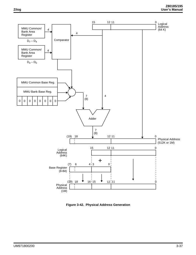
Physical Address Translation. Figure 3-42 shows theway in which physical addresses are generated based onthe contents of CBAR, CBR and BBR. MMU comparatorsclassify an access by logical area as defined by CBAR.Depending on which of the three potential logical areas(Common Area 1, Bank Area, or Common Area 0) is beingaccessed, the appropriate 8-bit base address is added tothe high-order 4 bits of the logical address, yielding a 20-bit physical address. CBR is associated with CommonArea 1 accesses. Common Area 0, if defined, is alwaysbased at physical address 00000H.
MMU and RESET. During RESET, all bits of the CA fieldof CBAR are set to 1 while all bits of the BA field of CBAR,CBR and BBR are reset to 0. The logical 64 KB addressspace corresponds directly with the first 64 KB (0000H toFFFFH) of the 1024 KB (00000H to FFFFFH) physical ad-dress space. Thus, after RESET, the Z80180 will begin ex-ecution at logical and physical address 0.
MMU Register Access Timing. When data is written intoCBAR, CBR or BBR, the value will be effective from the cy-cle immediately following the I/O write cycle which updatesthese registers.
Care must be taken during MMU programming to ensurethat CPU program execution is not disturbed. Observe thatthe next cycle following MMU register programming willnormally be an op-code fetch from the newly translated ad-dress. One simple technique is to localize all MMU pro-gramming routines in a Common Area that is always en-abled.
Figure 3-40. MMU Bank Base Register (BBR: I/O Address = 39H)
Bit
CB7 CB6
R/W
CB5
7 6 5 4 3 2 1 0
CB4 CB2 CB1 CB0
R/W
CB3
R/WR/WR/WR/WR/WR/W
Figure 3-41. MMU Bank Base Register (BBR: I/O Address = 39H)
Bit
BB7 BB6
R/W
BB5
7 6 5 4 3 2 1 0
BB4 BB2 BB1 BB0
R/W
BB3
R/WR/WR/WR/WR/WR/W
Z80185/195Zilog User’s Manual
UM971800200 3-37
3
Figure 3-42. Physical Address Generation
MMU Common/Bank AreaRegister
MMU Common/Bank AreaRegister
D7 – D4
D3 – D0
4
4
Comparator
4
15 12 11 0LogicalAddress(64 K)
MMU Common Base Reg.
MMU Bank Base Reg.
Adder
Physical Address(512K or 1M)
0 0 0 0 0 0 0 0
7(8)
4
(19) 12 11 0
7(8)
18
12 11 0
+
15
(7) 6 04 3Base Register
(8-Bit)
Physical
(1M)
(19) 12 11 018
Address
16 15
LogicalAddress
(64K)

Z80185/195User’s Manual Zilog
3-38 UM971800200
3.9 DYNAMIC RAM REFRESH CONTROL
The Z80185/195 incorporates a dynamic RAM refreshcontrol circuit including 8-bit refresh address generationand programmable refresh timing. This circuit generatesasynchronous refresh cycles inserted at the programma-ble interval independent of CPU program execution. Forsystems which do not use dynamic RAM, the refresh func-tion can be disabled.
When the internal refresh controller determines that a re-fresh cycle should occur, the current instruction is inter-rupted at the first breakpoint between machine cycles. The
refresh cycle is inserted by placing the refresh address onA0-A7 and the RFSH output is driven Low.
Refresh cycles may be programmed to be either 2 or 3clock cycles in duration by programming the REFW (Re-fresh Wait) bit in the Refresh Control Register (RCR). Notethat the external WAIT input and the internal wait stategenerator are not effective during refresh. Figure 3-43shows the timing of a refresh cycle with a refresh wait(TRW) cycle.
Figure 3-43. Refresh Cycle Timing
TR1 TRW* TR2
φ
Refresh
MREQ
RFSH
Refresh Signal
MCi MCi + 1Refresh Cycle
(internal signal)
Address A0-A7
Note: * If three refresh cycles are specified, TRW, is inserted. Otherwise, TRW is not inserted.MC = Machine Cycle

Z80185/195Zilog User’s Manual
UM971800200 3-39
3
Refresh Control Register (RCR). The RCR specifies theinterval and length of refresh cycles, while enabling or dis-abling the refresh function.
REFE: Refresh Enable (bit 7). REFE = disables the re-fresh controller while REFE = 1 enables refresh cycle in-sertion. REFE is set to 1 during RESET.
REFW: Refresh Wait (bit 6). REFW = 0 causes the re-fresh cycle to be two clocks in duration. REFW = 1 causesthe refresh cycle to be three clocks in duration by adding arefresh wait cycle (TRW). REFW is set to 1 during RESET.
Figure 3-44. Refresh Control Register (RCA: I/O Address = 36H)
T1 T2 T3 T1 T2 TTP T3 Ti Ti T1 T2 T3 T2 T3 T1T1 T2
A0-A18 (A19)
φ
D0-D7
PC 0000HSP-1
Undefined
MREQ
M1
RD
WR
T3
SP-2
Op-code
PC-1H PC-1L
3nd Op-codeFetch Cycle PC Stacking
Op-codeFetch Cycle
Restart
Memory
IX + d, IY + d
Ti Ti
Read Cycle
from 0000H

Z80185/195User’s Manual Zilog
3-40 UM971800200
CYC1, 0: Cycle Interval (bit 1,0). CYC1 and CYC0 spec-ify the interval (in clock cycles) between refresh cycles. Inthe case of dynamic RAMs requiring 128 refresh cycles ev-ery 2 ms (0r 256 cycles in every 4 ms), the required refreshinterval is less than or equal to 15.625 µs. Thus, the under-lined values indicate the best refresh interval dependingon CPU clock frequency. CYC0 and CYC1 are cleared to0 during RESET (see Table 3-6).
Refresh Control and Reset. After RESET, based on theinitialized value of RCR, refresh cycles will occur with aninterval of 10 clock cycles and be 3 clock cycles in dura-tion.
Dynamic RAM Refresh Operation Notes
1. Refresh Cycle insertion is stopped when the CPU is inthe following states:
a. During RESET
b. When the bus is released in response toBUSREQ.
c. During SLEEP Mode.
d. During WAIT states.
2. Refresh cycles are suppressed when the bus isreleased in response to BUSREQ. However, therefresh timer continues to operate. Thus, the time atwhich the first refresh cycle occurs after the Z80180re-acquires the bus depends on the refresh timer andhas no timing relationship with the bus exchange.
3. Refresh cycles are suppressed during SLEEP Mode.If a refresh cycle is requested during SLEEP Mode,the refresh cycle request is internally "latched" (untilreplaced with the next refresh request). The "latched"refresh cycle is inserted at the end of the first machinecycle after SLEEP Mode is exited. After this initialcycle, the time at which the next refresh cycle occursdepends on the refresh time and has no relationshipwith the exit from SLEEP Mode.
4. Regarding note 2 and 3 above, the refresh address isincremented by one for each successful refresh cycle,not for each refresh. Thus, independent of the numberof "missed" refresh requests, each refresh bus cyclewill use a refresh address incremented by one fromthat of the previous refresh bus cycles.
© 1998 by Zilog, Inc. All rights reserved. No part of thisdocument may be copied or reproduced in any form or byany means without the prior written consent of Zilog, Inc.The information in this document is subject to changewithout notice. Devices sold by Zilog, Inc. are covered bywarranty and patent indemnification provisions appearingin Zilog, Inc. Terms and Conditions of Sale only.
ZILOG, INC. MAKES NO WARRANTY, EXPRESS,STATUTORY, IMPLIED OR BY DESCRIPTION,REGARDING THE INFORMATION SET FORTH HEREINOR REGARDING THE FREEDOM OF THE DESCRIBEDDEVICES FROM INTELLECTUAL PROPERTYINFRINGEMENT. ZILOG, INC. MAKES NO WARRANTYOF MERCHANTABILITY OR FITNESS FOR ANYPURPOSE.
Zilog, Inc. shall not be responsible for any errors that mayappear in this document. Zilog, Inc. makes no commitmentto update or keep current the information contained in thisdocument.
Zilog’s products are not authorized for use as criticalcomponents in life support devices or systems unless aspecific written agreement pertaining to such intended useis executed between the customer and Zilog prior to use.Life support devices or systems are those which areintended for surgical implantation into the body, or whichsustains life whose failure to perform, when properly usedin accordance with instructions for use provided in thelabeling, can be reasonably expected to result insignificant injury to the user.
Zilog, Inc. 210 East Hacienda Ave.Campbell, CA 95008-6600Telephone (408) 370-8000FAX 408 370-8056Internet: http://www.zilog.com
Table 3-5. DRAM Refresh Intervals
Processor Interval (in microsec)
CYC1 CYC0InsertionInterval 20 MHz
Ø: 10 MHz 8 MHz
0 0 10 states 0.5 1.0 µ 1.250 1 20 states 1.0 2.0 2.5 1 0 40 states 2.0 4.0 5.0 1 1 80 states 4.0 8.0 µ 10.0