Haps-54 March2009 Manual
74
HAPS High-performance ASIC Prototyping System Motherboard HAPS-54
description
ASIC Prototyping
Transcript of Haps-54 March2009 Manual

HAPS
High-performance ASIC Prototyping System
MotherboardHAPS-54

2 HAPS-54High-performance ASIC Prototyping System
Revision History
Date Name Comment
Sep 04, 2007 Bo Nilsson Initial versionSep 05, 2007 Bo Nilsson Corrected GCLK numbering in table 9 and 11Sep 17, 2007 Bo Nilsson Cooling fans are not mounted on delivery (p. 3, 44)
Cut the VCCO wires before connecting together GPIO headers (p. 24, 56)Sep 27, 2007 Bo Nilsson Minor correctionsOct 04, 2007 Bo Nilsson Minor correctionsNov 13, 2007 Bo Nilsson p43: ALERT LED lights green indicating no overheatingNov 14, 2007 Bo Nilsson p69: Added pin numbers for the connectorsNov 23, 2007 Bo Nilsson p59, 60: Corrected bank numbers in HapsTrak connectors 4 and 7Dec 03, 2007 Bo Nilsson p10: Updated fig 3Dec 10, 2007 Bo Nilsson p37: Create lower frequencies with internal PLLs
p41: Updated text about SPI Flash PROMsJan 09, 2008 Bo Nilsson Updated fig 45, 60, 61 and 62Feb 04, 2008 Bo Nilsson Updated table “Global Clocks” on page 66Feb 07, 2008 Bo Nilsson p24: Updated fig 26Mar 18, 2008 Bo Nilsson STB2_1x1 replaces STB1_1x1 – Updated the Self-TestApr 02, 2008 Bo Nilsson p66: Renamed A_RESET, etc to A_RESET_n, etcMay 15, 2008 Bo Nilsson Updated section “Board Setup”Jun 26, 2008 Bo Nilsson p49: OSC2 default is 52 MHz
HAPS SupportNet is moved to http://hapssupportnet.synplicity.comNov 17, 2008 Bo Nilsson p3: Support is now on SolvNet. Documentation is still on SupportNet.Dec 03, 2008 Bo Nilsson p34: Output frequency from single-ended PLL defined up to 266 MHzFeb 26, 2009 Bo Nilsson p43: Updated table 13 (Power Good LED)Mar 11, 2009 Bo Nilsson p17: Updated figure 12; p69: Added delay for global signals between FPGAsMar 20, 2009 Bo Nilsson p63, 64: Corrected the indexes for the tables A-B and D-C
HAPS-54© 2009, Synopsys, Inc. March 20, 2009
S/N

3HAPS-54High-performance ASIC Prototyping System
Synopsys, Inc.
General Information
Contents of the boxA basic HAPS-54 delivery contains the following: This manual The manual “HAPS Interconnect Boards & Cables” The manual “Custom Daughter Boards” The STB2_1x1 User Guide 1 CD with manuals, application notes and design files 1 HAPS-54 board with 4 Xilinx Virtex-5 LX330 devices in FF1760 packages 2 interconnect boards CON_1x2 4 interconnect boards CON_2x1B 1 interconnect board CON_2x2 1 interconnect cable CON_CABLE40 2 TERM-TOP_1x1 1 STB2_1x1 (Self-Test Board) for testing the HAPS-54 board 1 LAB_1x1 experiment board 2 ribbon cables for GPIO, 320 mm [order code: HX-GPIO_CABLE] 7 MMCX coax cables, 300 mm [order code: HX-MMCX_CABLE] 1 RS232/SERIAL cable, [order code: HX-RS232_DATAPORT] 1 RS232/USB cable, [order code: HX-RS232_USB] 4 fans to be mounted on the FPGAs, [order code: HX-EBF42.5] 1 power cable (ATX MiniFit to Phoenix FMC plug), [order code: HX-ATX_ADAPTER] A sample of 5 HapsTrak II socket connectors (ASP-125516-03) 1 wrist strap
Power RequirementA complete system with HAPS-54 and daughter boards may require as much as 40A on 5V.Use a power supply such as TP-II 550PEC from Antec (http://www.antec.com).
Technical SupportThis manual contains all information you need to use the HAPS-54 motherboard. For each standard daughter board you are using, you should refer to the documentation provided with that board. If you want to design your own daughter boards, please see the manual “Custom Daughter Boards”.
Technical support is available on SolvNet at https://solvnet.synopsys.com.
SupportNetFor registered customers we offer complete documentation of all HAPS products. Please register at http://hapssupportnet.synplicity.com.
On SupportNet you will find the latest releases of all HAPS manuals, application notes, board files, HapsMap and other useful information.

4 HAPS-54High-performance ASIC Prototyping System
Synopsys, Inc.
ContentsRevision History ............................................................2
General Information .............................................................3Contents of the box ........................................................3
Power Requirement ..................................................3Technical Support ..........................................................3
SupportNet ................................................................3Overview ................................................................................6
Features ..........................................................................6Concept ..........................................................................8
Daughter Boards .......................................................8Inter-FPGA Connections ...........................................9Height Dimension Rules .........................................10Example of a HAPS System ...................................10HapsTrak .................................................................11
Board Layout Top Side ................................................12Board Layout Bottom Side ..........................................13I/O Signals & Interconnects ........................................15
VCCO Regions .........................................................15I/O Signals ..............................................................15Inter-FPGA Connections .........................................16General Purpose I/Os ..............................................16
Clocks ..........................................................................16Getting Started ....................................................................18
Applying Power the First Time ...................................18Test the Board ..............................................................19Adding Daughter Boards .............................................19Connecting Clocks.......................................................20Board Setup (SETUP switch) ......................................20Power-Up .....................................................................20Board Setup (Advanced Options) ................................20Configuring the Devices ..............................................21Reset & Reconfigure ....................................................22
Expansion and I/Os .............................................................23HapsTrak II Connectors ...............................................23
Signal Levels and I/O Standards .............................24GPIOs ..........................................................................24
Power ....................................................................................25VCCO Regions ..............................................................25VCCO in the HapsTrak II Connectors ..........................27Battery .........................................................................27
Clocks ...................................................................................28Clock Generators .........................................................28Global Single-Ended 1-to-1 Clocks .............................29Global Differential PLL Clocks ...................................31Global Single-Ended PLL Clocks ...............................33

5HAPS-54High-performance ASIC Prototyping System
Synopsys, Inc.
Direct Clocks ...............................................................35Synchronizing Clocks ..................................................36
Direct coax inputs ...................................................37Using a PLL to synchronize clocks ........................37Distributing clock hierarchies .................................37
Local Clocks ................................................................38Configuration.......................................................................39
JTAG Cable .................................................................40SPI Flash PROMs ...................................................41
CompactFlash ..............................................................42Board Status ........................................................................43
Voltage Monitoring ......................................................43Temperature Monitoring ..............................................43Self-Test .......................................................................44
Board Setup .........................................................................46Board Supervisor Registers .........................................47Setup via the Data Port ................................................54
Advanced Options ...............................................................56VCCO in the Bottom Side Connectors ..........................56GCLK_IN – parallel termination .................................57
Design Considerations ........................................................58Part Reference .....................................................................59Pin Tables .............................................................................60
HapsTrak II Connectors 1-3....................................60HapsTrak II Connectors 4-6....................................61HapsTrak II Connector 7 ........................................62Inter-FPGA Connections A-B (fast) .......................63Inter-FPGA Connections A-B (slow) ......................63Inter-FPGA Connections D-C (fast) .......................64Inter-FPGA Connections D-C (slow) .....................64Inter-FPGA Connections A-D (fast) .......................65Inter-FPGA Connections B-C (fast) .......................66HapsTrak CDE In ...................................................67HapsTrak CDE Out .................................................67Global Clocks .........................................................68Direct Differential Clocks .......................................68RESET ....................................................................68GPIO .......................................................................68
Signal Delays........................................................................69Connectors to FPGAs .............................................69FPGA to FPGA .......................................................69
Layout ..................................................................................70Board Dimensions ...............................................................71The Experiment Board LAB_1x1 ......................................72

6 HAPS-54High-performance ASIC Prototyping System
Synopsys, Inc.
OverviewHAPS-54 is a versatile multi-FPGA board intended for ASIC prototyping and HW/SW co-verification. It is designed for all ASIC prototyping needs, including HW/SW co-de-velopment, proof-of-concept studies, IP development and end user evaluations. The flex-ibility allows the same board to be reused in several projects or configurations by replacing daughter boards containing I/O and custom subsystems.
The 26-layer board is carefully designed for maximum performance, with respect to signal integrity, speed and other critical issues. Signals to connectors and between FPGAs are length matched, thus minimizing skew and allowing very high speed signaling.
The modular system with daughter board connectors placed in an equidistant matrix (70x50 mm), as on all HAPS boards, allows any daughter board to be placed anywhere in the matrix.
Several standard daughter boards are available: See http://www.synplicity.com for an up-to-date listing.
Features 4 Xilinx Virtex-5 LX330 devices in FF1760 packages 13 VCCO regions
9 regions can individually be adjusted to: 3.3, 2.5, 1.8, 1.5, or 1.2 V All 13 regions can be sourced externally for other voltages 3632 signals for I/O and inter-FPGA connection 2856 I/Os (LVDS as an option) in 24 HapsTrak II connectors 736 predefined inter-FPGA connections 466 fixed 32 available for SelectMap configuration 238 available in four HapsTrak II connectors for expansion to other motherboards 40 GPIOs 16 global clocks, sourced externally or generated on-board
All clocks can be sourced from the FPGAs 2 PLLs, one single ended and one differential 2 external differential clocks to each FPGA 208 local clocks – differential or single-ended 3 on-board programmable clock generators Configuration via JTAG, on-board SPI Flash PROMs, SelectMAP or
optionally from a CompactFlash card High speed routing – High speed I/O or TDM (Time Domain Multiplexing) of
inter-FPGA signals for high-connectivity designs Configurable routing – The existing buses between pairs of FPGAs are easily
expanded by standard interconnect boards or cables On-board temperature and voltage watchdog Temperature controlled fan drivers Built-in self-test Battery backed-up encryption key Single +5 V power supply HapsTrak I & II compatible

7HAPS-54High-performance ASIC Prototyping System
Synopsys, Inc.
The HAPS-54 motherboard is equipped with 4 Virtex-5 devices, 24 HapsTrak II termi-nal connectors on the top side of the board, and 24 socket connectors on the bottom side. The connectors are divided into 13 different VCCO regions. The voltages are set with DIP switches and are available in terminals for external use. Four additional HapsTrak II ter-minal connectors on the top side form two global buses with 2.5V VCCO.
HAPS-54 requires a single +5 V power supply to operate. All other voltages are gen-erated on-board.
The FPGA devices can be configured either via a JTAG cable or from a Compact-Flash memory. For CompactFlash configuration the board CONF30 can be used (not included in the delivery).
Virtex-5 LX330
GN
D
JTAG out
JTAG CFG
ALERT LEDRESET LED
OSC 1,2,3 out
HapsTrak CDE in
HapsTrak CDE out
DC/DC converters
Glo
bal b
usG
loba
l bus
Glo
bal b
usG
loba
l bus
GPIOGPIO LEDs
5V IN
PW
R o
n LE
D
Batte
ryGlobal clock in
Global clock out
ResetReconfigure
Board Supervisor
Mode select
Configuration LEDs
Select LEDs
Select LEDs
Sel
ect L
ED
s
VCCO LEDsV3a adjust
V1b
adju
st
V2c
adju
stV3b adjust
V3c adjust
V1c
adju
st
V1a adjust
V2a adjust
V2b
adju
st
Frequency select
Optional oscillators
Differential PLL in
Differential PLL out
Single ended PLL in
Single ended PLL out
HapsTrak IIconnectors
JTAG in
CONF
(factory testing)
V3a
in/o
utV
3ax
in
V3c in/outV3cx in
V1a
x in
V1a
in/o
ut
V1c
x in
V1c
in/o
ut
V1b
in/o
ut
V2b in/out
V2c in/out
V3b in/out
V2a in/out
Holes to securedaughter boards
Holes to securedaughter boards
Direct clocks
Fan connectors
Dat
a po
rt
Test
poi
nts
Power-good LED
A
B
D
C
Fig 1. The HAPS-54 motherboard

8 HAPS-54High-performance ASIC Prototyping System
Synopsys, Inc.
ConceptA HAPS system consists of at least one motherboard. The motherboard is merely a logic container with the biggest FPGAs in the biggest packages.
High quality connectors for I/Os and inter-FPGA buses are placed in a regular 70x50 mm matrix. Each FPGA is connected to a group of these connectors. Each connector has dedicated pins for power and for clocks.
Dedicated clock inputs on the FPGA devices are connected to global clocks. The low skew, high-speed clocks are distributed by clock buffers. The clocks can be driven either externally, from the FPGAs or from on-board oscillators.
Fixed buses connects the FPGAs together. Wider buses are easily created by low cost interconnect boards. Parts of the buses are connected to two pairs of HapsTrak connec-tors, which can be used to expand the buses to other motherboards. Each FPGA also has a number of GPIO.
Ordinary daughter boards, like memory boards and interface boards can be placed on any connector. The size of a daughter board is strictly specified. There are no “wasted” connectors on the motherboard.
The dimensions of motherboards follow the same rules as for daughter boards. This means that motherboards can be placed side by side and connected together with standard interconnect boards. Since all HAPS motherboards have mating connectors on the bottom side they can also be stacked together like LEGO® bricks. All connectors conform to the HapsTrak standard.
Daughter Boards
Each daughter board mates with one or several connectors on the motherboard. The con-nectors are spaced evenly, so even a multi-connector daughter board can be moved around freely. This allows you to reconfigure the prototype system as parts of the design moves from one FPGA to another.
Most daughter boards also have a connector on the top side, opposite to the connec-tors that mate the HAPS motherboard. All signals are connected straight through the board. This allows several daughter boards to be stacked on top of each other, and have access to the same FPGA signals. In some boards, certain signals (typically enable signals) are “staggered” through the board stack, so that the motherboard can identify each board even though they share a common bus. Consult each daughter board manual for details.
Stacking of daughter boards also allows you to monitor signals in the connector with a logic analyzer while the system is running and the daughter board is still attached to the HAPS motherboard.
The board LAB_1x1, supplied with HAPS-54, has a prototype area where the signals in the connector are available for use on the board, see page 70.
The LAB_1x1 board alone is probably not sufficient to implement all your I/Os and subsystems. Look at http://www.synplicity.com to find our current list of standard daughter boards and try to find one that suits your needs. For special needs, we can develop custom daughter boards according to your specifications, or provide you with PCB layout templates that enable you to create your own daughter boards. See details about custom daughter boards in the manual “Custom Daughter Boards”.
LEGO® is a trademark of the LEGO Group of companies which does not sponsor, authorize or endorse the HAPS product.

9HAPS-54High-performance ASIC Prototyping System
Synopsys, Inc.
C
HapsTrak
HapsTrak
HapsTrak
HapsTrak
HapsTrak
HapsTrak
HapsTrak
HapsTrak
HapsTrak
HapsTrak
HapsTrak
HapsTrak
HapsTrak
HapsTrak
HapsTrak
HapsTrak
HapsTrak
HapsTrak
HapsTrak
HapsTrak
HapsTrak
HapsTrak
G
G
G
G
FPGA
FPGA
FPGA
FPGA
50 mm
FPG
AFP
GA
70m
m70
mm
70m
m
Global bus
I/Os or inter-FPGAconnections
Fixed inter-FPGAconnections
Local clocks
G
C Global clocks
GPIO
Hap
sTra
kH
apsT
rak
Hap
sTra
kH
apsT
rak
External
Internal
HapsTrak HapsTrak
Fig 2. A HAPS motherboard
Inter-FPGA Connections
All daughter board connectors can be used either for I/O or for creating wider buses be-tween the FPGAs. In fact they can even be used for a combination of both.
A number of standard interconnect boards and cables are available from Synplicity.
CON_2x1B connects 119 signals between two FPGAs perpendicular to the connectors
CON_1x2 as CON_2x1B but along the connectors CON_2x2 creates diagonal buses or a 4-way bus between four FPGAs CON_CABLE connects any daughter board connector to any other
Look at http://www.synplicity.com to find a current list of interconnect boards.

10 HAPS-54High-performance ASIC Prototyping System
Synopsys, Inc.
Height Dimension Rules
70 mm
19 mm
* 5 mm
~ 2.4 mm motherboard
daughter board 1
daughter board 2
max 3 mm
for stackable daughter boardsthere is a height limit
HX-QTH-YYY-05
HX-QSH-YYY-01
* HX-QTH-YYY-XX
* ConnectorHX-QTH-YYY-01
0305
HX-QTH-YYY-HX-QTH-YYY-
Mating height5 mm11 mm19 mm
YYY = 060 or 064YYY = 060 or 064YYY = 060 or 064
Fig 3. Height dimensions
Example of a HAPS System
HAPS boards can be connected together in many ways. Below is an example just to point out some important features with the HAPS concept. Notice the similarity to building with LEGO® bricks.
FPGAFPGA HAPS-54
The physical dimensions fordaughter are strictlyspecified. All connectors canbe used.
boards
Connectors at differentheights can be alignedwith extenders.
Motherboards canbe stacked on topof each other.
Motherboards canbe connected withinterconnect s.board
Boards can bestacked in avariety of ways.
Buses betweenFPGAs are expandedwith interconnect s.board
A Mictor board with logicanalyzer headers canbe placed on top ofeverything.
Daughter boardscan be stacked ontop of each other.
Most boards haveconnectors on bothsides.
Daughter boardsare placed on thesame connectorsused for creatingbuses.
Daughter boards can beplaced on the bottomside of a motherboard.
FPGAFPGA HAPS-34
FPGAFPGA HAPS-54
FPGA HAPS-52 FPGA HAPS-51
Fig 4. Example of a HAPS system
11HAPS-54High-performance ASIC Prototyping System
Synopsys, Inc.
HapsTrak
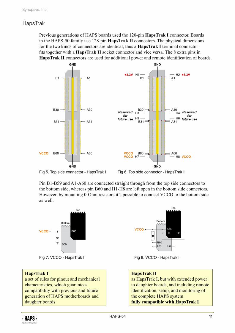
Previous generations of HAPS boards used the 120-pin HapsTrak I connector. Boards in the HAPS-50 family use 128-pin HapsTrak II connectors. The physical dimensions for the two kinds of connectors are identical, thus a HapsTrak I terminal connector fits together with a HapsTrak II socket connector and vice versa. The 8 extra pins in HapsTrak II connectors are used for additional power and remote identification of boards.
Fig 5. Top side connector - HapsTrak I Fig 6. Top side connector - HapsTrak II
Pin B1-B59 and A1-A60 are connected straight through from the top side connectors to the bottom side, whereas pin B60 and H1-H8 are left open in the bottom side connectors. However, by mounting 0-Ohm resistors it’s possible to connect VCCO to the bottom side as well.
B60
0
VCCO
Bottom
B60
Top
H7B60
H8
0
Bottom
H7B60
H8
Top
VCCO
Fig 7. VCCO - HapsTrak I Fig 8. VCCO - HapsTrak II
HapsTrak IIas HapsTrak I, but with extended power to daughter boards, and including remote identification, setup, and monitoring of the complete HAPS systemfully compatible with HapsTrak I
HapsTrak Ia set of rules for pinout and mechanical characteristics, which guarantees compatibility with previous and future generation of HAPS motherboards and daughter boards

12 HAPS-54High-performance ASIC Prototyping System
Synopsys, Inc.
Board Layout Top Side
AXC5VLX330
CXC5VLX330
BXC5VLX330
V3ax
GND
V3a
C7 2.5VB7 2.5V
D7 2.5VA7 2.5V
Frequencyselect
DC/DC3.3V
DC/DC2.5V
DC/DCV2b
DC/DCV2c
DC/DCV1b
DC/DCV1c
DC/DCV3b
DC/DCV3c
DC/DCV2a
DC/DCV1a
DC/DCV3a
X BA CD
X BA CD
X BA CD
RECONFIGURE RESET
OSC
1 102 3 4 5 6 87 9
ON
1 102 3 4 5 6 87 9
ON
1 102 3 4 5 6 87 9
ON
DRIVE
5V
TACH
DRIVE
5V
TACH
DRIVE
5V
TACH
DRIVE
5V
TACH
OSC
OSC
INIT_B
GND
GND
3.3 V
3.3 V
PROG_B
DONE B
DONE A
TMSTCKTDOTDI
+2.5 V
GNDGNDGNDGNDGNDGNDGND
DATAPORT
CTS
RXD
GND
GND
TXD
RTS
2.5VB2 N_B2 P_
B3 N_B3 P_GND
2.5V
GNDJ.A.PU
ALL DONE_
TDOPU
GND
VCCTMSTCKTDOTDI
CHAINED_n
GNDGNDGNDGNDGNDGND
2.5V
1.8V
1.5V
PWR
3.3V
1 2 3 4 5
ON
2.5V
1.8V
1.5V
PWR
3.3V
1 2 3 4 5
ON
2.5V
1.8V
1.5V
PWR
3.3V
1 2 3 4 5
ON
2.5V
1.8V
1.5V
PWR
3.3V
1 2 3 4 5
ON
2.5V
1.8V
1.5V
PWR
3.3V
1 2 3 4 5
ON
2.5V
1.8V
1.5V
PWR
3.3V
1 2 3 4 5
ON
2.5V
1.8V
1.5V
PWR
3.3V
1 2 3 4 5
ON
offon
7 8 9 10654321
OVERRIDESETUP
1 102 3 4 5 6 87 9
ON
DC/DCVCCINT C
DC/DCVCCINT D
DC/DCVCCINT B
2.5V
1.8V
1.5V
PWR
3.3V
1 2 3 4 5
ON
2.5V
1.8V
1.5V
PWR
3.3V
1 2 3 4 5
ON
Battery
DC/DCVCCINT A
GND1
V1cx 2 3 4 5
6 7 8 9 10 GND
V1c
61
GND1V3c 2 3 4 5
6 7 8 9 10 GND
V3cX
61
GND1V3a 2 3 4 5
6 7 8 9 10 GND
V3ax
GND1
V1ax 2 3 4 5
6 7 8 9 10 GND
V1a
61
61
VCCAUX C
Voltage regulator
VCCAUX B
Voltage regulator
VCCAUX D
Voltage regulator
VCCAUX A
Voltage regulator
PWRON
A1
V1ax
A3
V1a
A2
V1b
A4
V1b
A5
V2a
A6
V2b
B2V2b
B1
V2a
B6
V3b
B4
V3b
B5
V3ax
B3
V3a
D1
V1b
D3
V1b
D5
V2b
C1
V2b
C5
V3b
C3
V3b
D2
V1cxD4
V1c
D6
V2c
C2
V2c
C6
V3cx
C4
V3c
V1ax
GND
V1a
V2aGND
V2bGND
V2cGND
V1b
GND
V1cx
GND
V1c
V3b
GND
V3cx
GND
V3c
Fan B Fan C
Fan A FanD
N P
GC_B1
N P
GC_C1
N P
GC_C2
N P
GC_B2
N P
N P
GC_D2
GC_D1
N P
N P
GC_A2
GC_A1
21
345
GCLK_IN
6789
12345
GCLK_OUT
6789
JTAGIN
CONF
JTAGOUT
JTAG CFG
B
Power Good
DONEA
C
D
offon
offon
offon
OVERRIDE
OVERRIDE
OVERRIDEDONE C
DONE D
PWR_GR
factory test only
RESET ALERT
V3a
V2a
V1a
V3b
V2b
V1b
V3c
V2c
V1c
1
2
37 8 9 10654321
a b
a b
DIFFERENTIAL
SINGLE
ENDED
REFp
REFn
FBp
FBn
1p
1n
2p
2n
REF
FB
1
2
3
4
5
6
OUT
OUT
8A
8B
9A
9B
REFB+
REFB-
FBA+
FBA-
REFB+
FBA+
6A
6B
7A
7B
8A
9A
ININ
GBGPIO B
GAGPIO A
GCGPIO C
GDGPIO D
OSC1
OSC2
OSC3
1
2
3
DXC5VLX330
GND 5V
CDEOut
CDEIn
BOARDSUPERVISOR
Fig 9. HAPS-54 - top side

13HAPS-54High-performance ASIC Prototyping System
Synopsys, Inc.
Board Layout Bottom Side
A1
V1ax
A3V1a
A2
V1b
A4
V1b
A5
V2a
A6
V2b
B2
V2b
B1
V2a
B6
V3b
B4
V3b
B5
V3ax
B3
V3aD1
V1b
D3
V1b
D5
V2b
C1
V2b
C5
V3b
C3
V3b
D2
V1cx
D4
V1c
D6
V2c
C2
V2c
C6
V3cx
C4
V3c
AXC5VLX330
CXC5VLX330
BXC5VLX330
DXC5VLX330
U47
UC5
UC13
U135
UC4
U107
U116
UD10
U48
U38
U55
U104
U105
U28
U128
UC12
U66
U98
U120
U82
U61
U29
UD4
UA12
UD11
U39
U134
U97
U32
U78
X3
U123
U68
UA10
U89
U59
U92
U109
UA9
U133
U121
UA11
U103
U72
U9 UA4
U27
UC9
U13
U51
U42
U21
U115
U95
U117
U111
U84
UD5
U57
U71
U45
UB9
U50
U86
U12
U46
U76
U96
U87
U118
U79
UA14
U145
UB8
UB5U127
UA5
U140
U43
U90
U65
U33
U113
U30
UB11
UA13
UB10
U41
U31
U101
U53
U34
U26
U56
U35
U37
U102
UD12
U83
U119
U85
U40
U91
U22
U62
U99
U146
U60
U23
U52
U54
U64
U77
X2
U49
U36
U10
UC11
UB12
UA8
U69
UC8
X1
U14U141
U129
U114
U139
U94
U70
U25
UD13
U24
U108
U93
U110
U122
U67
U88
U126
UD9
U58
UB13
UB4
UD8
UB14
U106
U100
U11
U44
UC10
UC14
UD14
Voltage regulator EEPROM
SIPO
Voltage regulator
Clockselect
Voltageregulator
Voltag eregulator
Temp monitor
14.7456MHz
Clockbuffers
PISO
SU Flash
Clock generator
Clock generator
Clock generator
Voltageregulator
SM-bus
SM-bus buffersTerminationregulator
SIPO
SIPO
Voltageregulator
PLL
PLL
MUX
SIPO
Voltageregulator
SIPO
MUX
RS-232
SPI Flash
SIPO
Buffer
SIPOSPI Flash
Temp monitor
Voltage monitor
SIPOSIPO
PISO
Level shifters
SIPO
SIPO
Temp monitor
PISO
SPI Flash
Buffer
Buffer
SPI Flash
Temp monitor
Fig 10. HAPS-54 - bottom side

14 HAPS-54High-performance ASIC Prototyping System
Synopsys, Inc.
The main components of a HAPS-54 board are:
4 Virtex-5 FPGAs (LX330) 24 HapsTrak II terminal connectors (128 pins, mating height 19 mm) 24 HapsTrak II socket connectors on the bottom side (128 pins) 4 HapsTrak II connectors (128 pins, mating height 11 mm)1
1 HapsTrak CDE In socket connector (60 pins) 1 HapsTrak CDE Out terminal connector (60 pins) 4 headers (2x7) for 4x10 GPIOs 2 headers (2x7) for JTAG, in and out 1 header (2x3) for JTAG configuration 1 header (2x7) for the CONF30 board 1 RJ11 connector for board setup and monitoring (Data Port) 4 headers (1x3) for fan driving 9 MMCX global clock inputs 2x9 MMCX global clock outputs 4 MMCX differential PLL clock inputs 4 MMCX differential PLL clock outputs 2 MMCX single ended PLL clock inputs 6 MMCX single ended PLL clock outputs 4x2 MMCX differential direct clock inputs for each FPGA 3 on-board programmable clock generators 3 sockets for alternative reference oscillators 9 DIP switches (5-pole) to set VCCO 1 DIP switch (10-pole) to set the clock source 3 DIP switches (10-pole) to set oscillator frequencies 1 terminal for +5 V: 5 pins for GND and 5 pins for +5 V 9 terminals for VCCO: 5 of them 2-pole, 4 of them 3-pole 4x11 yellow mini LEDs indicating clock sources 9x4 yellow mini LEDs indicating VCCO voltage levels 17 yellow mini LEDs indicating if DIP switch values are overridden 12 LEDs: 1 +5V, 1 Power Good, 4 DONE, 1 RESET, 1 ALERT, 4 GPIO 1 header (2x7) for factory testing 1 reset button 1 reconfigure button 1 socket for an optional battery
1 Boards with serial number 070647 and above. Previous versions had HapsTrak I connectors!

15HAPS-54High-performance ASIC Prototyping System
Synopsys, Inc.
I/O Signals & Interconnects
V3b
A7 D7
B7 C7
2.5V 2.5V
2.5V 2.5V
119 119
V1b
167167
66
66
B_GPIO
A_GPIO
C_G
PIO
D_G
PIO
10
10
119 119
119 119
119 119
119 119
119 119
119 119
119 119
119 119
119 119
119 119
119 119119 119
10
10
A D
B C
A5
D5
A3
D3
A6
D6
A4
D4
B5
C5
B3
C3
B4
C4
B2
C2
A1
D1
B6
A2
V3b
2.5V
1.8V
1.5V
PWR
3.3V
1 2 3 4 5
ON
GN
D
V3b
V2b2.5V
1.8V
1.5V
PWR
3.3V
1 2 3 4 5
ON
GN
D
V2b
V1b
2.5V
1.8V
1.5V
PWR
3.3V
1 2 3 4 5
ON
GN
D
V1b
B1
C1
C6
D2
29332521
30 342622
28 322420
27312319
34 26
30 22
33 25
29 21
18 12
14 16
17 11
13 15
20 28
24 32
19 27
23 31
34 26
30 22
33 25
29 21
18 12
14 16
17 11
13 15
20 28
24 32
19 27
23 31
8
7
6
5
8
7
6
5
AB AB
34 26
30 22
33 25
29 21
18 12
14 16
17 11
13 15
20 28
24 32
19 27
23 31
34 26
30 22
33 25
29 21
18 12
14 16
17 11
13 15
20 28
24 32
19 27
23 31
8
7
6
5
8
7
6
5
AB AB
29332521
111517 13
27312319
75 31
24 6830 34
2622
161214 18
29332521
111517 13
75 31
24 6830 34
2622
161214 18
28 322420
75 31
27312319
111517 13
293325212
4 68
161214 18
28 322420
75 31
27312319
111517 13
24 6830 34
2622
161214 18
28 322420
20
18
19
17
18
34
17
33
V3c
2.5V
1.8V
1.5V
PWR
3.3V
1 2 3 4 5
ON
GN
D
V3c
V3cx
V3a
2.5V
1.8V
1.5V
PWR
3.3V
1 2 3 4 5
ON
V3ax
GN
D
V3a
V2a
2.5V
1.8V
1.5V
PWR
3.3V
1 2 3 4 5
ON
GN
D
V2a
V1a
2.5V
1.8V
1.5V
PWR
3.3V
1 2 3 4 5
ON
V1ax
GN
D
V1a
V1c
2.5V
1.8V
1.5V
PWR
3.3V
1 2 3 4 5
ON
GN
D
V1c
V1cx
V2c
2.5V
1.8V
1.5V
PWR
3.3V
1 2 3 4 5
ON
GN
D
V2c
33
33
45
111
56
28
28
167 inter-FPGA connects
V1a V3ax
V1ax V3a
V2b
2.5V
V2a
33
33
45
111
56
28
28
167 inter-FPGA connects
V1c V3cx
V1cx V3c
V2b
2.5V
V2c
32 2.5V
Fig 11. I/Os, interconnects, I/O banks and VCCO regions
VCCO Regions
All necessary voltages are generated on-board from a single +5 V power source. DC/DC converters generate the I/O voltages for the HapsTrak II connectors. These are divided into 13 independent VCCO regions, 9 of them individually configurable with DIP switches to 3.3 V, 2.5 V, 1.8 V, 1.5 V or 1.2 V. The regions, V1ax, V3ax, V1cx and V3cx can easily be connected to regions V1a, V3a, V1c, and V3c respectively. Connectors A7, B7, C7 and D7 are fixed at 2.5V.
If a voltage other than the predefined ones is required, the corresponding DC/DC converter can be switched off and the desired I/O voltage supplied from an external source.
I/O Signals
Each HapsTrak II connector is connected to an FPGA via 119 signals and three pins sourc-ing VCCO to daughter boards. Adjacent pins can be used as differential pairs.
16 HAPS-54High-performance ASIC Prototyping System
Synopsys, Inc.
16 of the pins are routed to clock capable inputs to the Virtex-5 devices, while 8 signals are routed to VREF inputs. A daughter board that requires an I/O standard that needs VREF will create the necessary VREF voltage and feed it to HAPS-54 on dedicated pins in the connec-tor. Daughter boards that don’t need VREF can use these pins as ordinary I/O.
Inter-FPGA Connections
The four FPGAs are connected together with totally 736 signals, with slightly different characteristics.
”Buried” Interconnects167 “buried” signals between the FPGAs A and B, and C and D respectively, can be di-vided into two groups: direct and via level shifters.66 “buried” direct signals between the FPGAs A and D, and B and C respectively.
Global BusThe HapsTrak II connectors A7 and B7 are connected together with FPGAs A and B, and connectors C7 and D7 are connected together with FPGAs C and D. These connectors are ideal for creating a global bus, even expanded to several motherboards. Use either cables (CON_CABLE40) or interconnect boards (CON_2x1B) to make the interconnect.
Termination boards (TERM-TOP_1x1) are recommended on the first and last con-nector in the chain. Termination boards TERM-TOP_1x1 are included in the delivery.
SelectMapThe 32 data signals in the SelectMap In bus can also be used as ordinary inter-FPGA bus. These signals are terminated on-board.
General Purpose I/Os
Each FPGA has 10 I/O signals available in headers. Two of the signals also drive a two-colored LED. These are used by the self-test to indicate if the hardware is faultless or not.
ClocksOn HAPS-54, 20 global clock pins (GC inputs, see Xilinx documentation) on each Virtex-5 device are dedicated for clock signals. 16 of these signals drive all FPGAs and are also available externally in MMCX connectors. Each of these 16 clocks can be sourced from either FPGA or externally, selectable with a DIP switch. 9 clocks are driven directly via high-speed clock buffers. 3 clocks are sourced by a PLL in single ended mode, and 2 dif-ferential clocks are driven by another PLL. The 4 remaining clock pins can also be used in differential mode, and are directly connected from MMCX connectors to the FPGAs.
Three on-board programmable clock generators are directly connected to MMCX connec-tors. The frequencies are set with DIP switches, but can also be altered by using reference oscillators with other frequencies. To use the clock signals in your design, just connect coax cables to any of the clock inputs, and do the pin assignment accordingly.

17HAPS-54High-performance ASIC Prototyping System
Synopsys, Inc.
X_GCLK0(1)
X_GCLK0(2)
X_GCLK0(3)
X_GCLK0(4)
X_GCLK0(5)
X_GCLK0(6)
X_GCLK0(7)
X_GCLK0(8)
X_GCLK0(9)
X_PLL_D
X_PLL_SE
Outputs from each FPGA Inputs to each FPGA
GCLK(1)
GCLK(2)
GCLK(3)
GCLK(4)
GCLK(5)
GCLK(6)
GCLK(7)
GCLK(8)
GCLK(9)
GCLK(14)
GCLK(15)
GCLK(16)
GCLK(17)
GCLK(19)
GCLK(18)
GCLK(20)
Same pinning for all FPGAs Same pinning for all FPGAs
GCLK(10)
GCLK(12)
Other FPGAs
D
C
B
A
mux ctrl
X
FB
mux
PLL ctrl
DIFFPLL
Other FPGAs
D
C
B
A
mux ctrl
X
FB
mux
PLL ctrl
SEPLL
Other FPGAs
D
C
B
A
X
mux ctrl
muxclkbuf
1 .. 9
GCLK(11)
GCLK(13)
ClockGenerator
ClockGenerator
ClockGenerator
frequencyselect
frequencyselect
frequencyselect
1 2 3
Fig 12. Clocks
Each FPGA also has 112 local clock pins (CC inputs, see Xilinx documentation) sourced from the HapsTrak II connectors.

18 HAPS-54High-performance ASIC Prototyping System
Synopsys, Inc.
Getting StartedRemember that the HAPS-54 board, as all other electronic equipment, is sensitive to static discharge. Make sure that you’re properly grounded whenever handling the board directly.
All positional references to the motherboard are made assuming that the board is placed in front of you as in the figure in the “Board Layout” section on page 12.
See SupportNet at http://hapssupportnet.synplicity.com for the latest version of this manual.
Applying Power the First TimeThe connector for power supply is the terminal block at the top of the board. The board requires only 5 V. All other voltages are generated on-board. The PWR ON LED indicates when 5 V is available, and the Power Good LED indicates if the on-board generated voltages are within tolerance. Both LEDs should light green.
The power connector is separated in two parts:– the header which is permanently soldered to the HAPS-54 board – the plug in which power (5 V) and ground (GND) cables are inserted
To disconnect the plug, pull firmly. Don’t use any of the HapsTrak connectors as support, as the soldering may break.
Use a small screwdriver to press the orange le-ver next to one of the holes. Insert a suitable (~ 1.5 mm2) cable in the hole and release the lever. This will secure the cable.
Notice that the hole in the middle is unused. This is to clearly separate the 5 V from GND. Five holes may be used as GND and 5 V, respectively.
To connect the plug, press firmly while supporting the board at the opposite end. As before, don’t use any of the HapsTrak connectors as support.
HAPS-54 requires about 4A at start-up and when the FPGA devices are unconfigured. Total power consumption of a configured HAPS board depends on mounted daughter boards, the design and the clock frequency. Consult the Xilinx manuals and web site for details of the FPGA current consumption. The other components on the board require negligible amounts of power in comparison to the FPGA devices.
GND 5V
Fig 13. Power supply connector
Fig 14. Power plug

19HAPS-54High-performance ASIC Prototyping System
Synopsys, Inc.
Adjust the VCCO voltages for the I/O voltage regions V1a, V2a, V3a, V1b, V2b, V3b, V1c, V2c and V3c by setting the nine DIP switches according to the table below. The regions V1ax, V3ax, V1cx and V3cx, are normally connected together with regions V1a, V3a, V1c and V3c, respectively.
Only one of the switches 1, 2, 3 and 4 should be in the on-position.
The voltages are measured by a voltage monitoring curcuit and the corresponding LEDs are turned on. If other voltages are needed, set the switch PWR to off and supply external power via the VCCO connectors.
V1a, V2a, V3a V1b, V2b, V3b V1c, V2c, V3c
DIP switch 1 2 3 4 5 VCCO
3.3V 2.5V 1.8V 1.5V PWR on off off off on 3.3 V off on off off on 2.5 V * off off on off on 1.8 V off off off on on 1.5 V off off off off on 1.2 V – – – – off disabled
* default
Default ondelivery
V2cGND
V1cx
GN
DV1
c
V3ax
GN
DV3
aV1
ax
GN
DV1
a V1b
GN
D
V2bGNDV2a
GND
Default ondelivery
Default ondelivery
V3b
GN
D
V3cx
GN
DV3
c
Default ondelivery
Table 1. VCCO values Fig 16. VCCO connectors
For more information, see section “Power”.
Test the BoardBefore using a complex electronic device like HAPS-54 it’s wise to do a sanity check. A design with a self-test suite is included on the CD. The test suite first checks for short circuits on the board and if the enclosed self-test board (STB2_1x1) is used, also for open circuits in the connectors. For details, see “Self-Test” in section “Board Status”.
The ALERT LED is blinking red if any of the FPGA devices is overheated.
Adding Daughter BoardsA good idea is to power up the board and check all VCCO voltages before plugging in daughter boards. Remember to turn off the power before mounting the daughter boards.
Most daughter boards have connectors placed along one of its edges. The connectors have a small chamfer that prevents the board from being mounted the wrong way. Press the daughter board gently into the selected connectors. If it doesn’t slide in easily, check the orientation of the board again. You have to use very little force, but be firm and make sure
2.5V
1.8V
1.5V
PWR
3.3V
1 2 3 4 5
ON ONOFF
Fig 15. VCCO setting
20 HAPS-54High-performance ASIC Prototyping System
Synopsys, Inc.
that you insert the board straight by pushing on both sides of the connector. A board insert-ed slightly ajar will not have a proper connection in all pins.Most daughter boards are powered through the daughter board connector, but some may need external power, perhaps by supplying power from the corresponding VCCO connector. Refer to the documentation of each board.
Small boards can be attached on a single connector and will stay put without any ad-ditional support. Larger boards are mounted on several connectors for mechanical stabil-ity, or have additional support stands. If needed, the daughter boards can be secured in the mounting holes on the motherboard.
Connecting ClocksConnect external clocks to the MMCX connectors. If you want to use the on-board oscil-lators you must connect a cable (included in the delivery) from one of the OSC outputs to one of the GCLK_IN inputs. If you run the self-test, you must connect a cable from OSC1a or OSC1b to GCLK_IN1.
The coax cables can be a bit tricky to detach from the MMCX connectors. Use a pair of pliers and pull straight upwards without using excessive force.
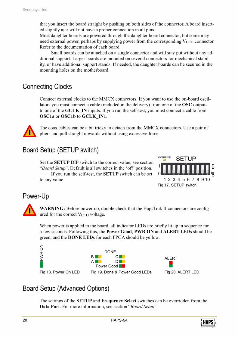
Board Setup (SETUP switch)Set the SETUP DIP switch to the correct value, see section “Board Setup”. Default is all switches in the ‘off’ position.
If you run the self-test, the SETUP switch can be set to any value.
Power-UpWARNING: Before power-up, double check that the HapsTrak II connectors are config-ured for the correct VCCO voltage.
When power is applied to the board, all indicator LEDs are briefly lit up in sequence for a few seconds. Following this, the Power Good, PWR ON and ALERT LEDs should be green, and the DONE LEDs for each FPGA should be yellow.
PWR
ON
B
Power GoodA
CD
DONE
ALERT
Fig 18. Power On LED Fig 19. Done & Power Good LEDs Fig 20. ALERT LED
Board Setup (Advanced Options)The settings of the SETUP and Frequency Select switches can be overridden from the Data Port. For more information, see section “Board Setup”.
off
on
7 8 9 10654321
OVERRIDE SETUP
1 102 3 4 5 6 87 9
ON
10
Fig 17. SETUP switch
21HAPS-54High-performance ASIC Prototyping System
Synopsys, Inc.
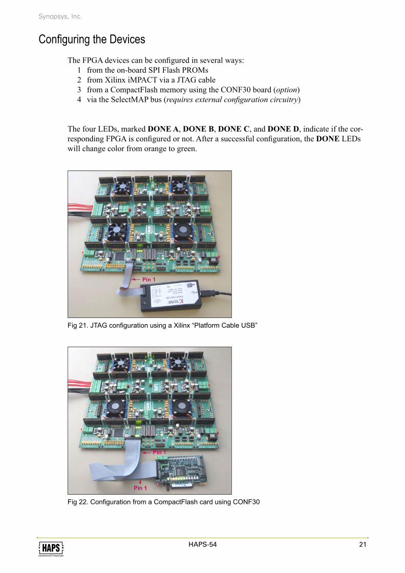
Configuring the DevicesThe FPGA devices can be configured in several ways:
1 from the on-board SPI Flash PROMs2 from Xilinx iMPACT via a JTAG cable3 from a CompactFlash memory using the CONF30 board (option)4 via the SelectMAP bus (requires external configuration circuitry)
The four LEDs, marked DONE A, DONE B, DONE C, and DONE D, indicate if the cor-responding FPGA is configured or not. After a successful configuration, the DONE LEDs will change color from orange to green.
Fig 21. JTAG configuration using a Xilinx “Platform Cable USB”
Fig 22. Configuration from a CompactFlash card using CONF30

22 HAPS-54High-performance ASIC Prototyping System
Synopsys, Inc.
Reset & ReconfigurePressing the RESET button will send an asynchronous reset to all FPGAs on pin L14. Pressing the RECONFIGURE button will empty the configuration memory of the FPGAs. When the button is released, they will read a configuration data stream from the on-board SPI Flash PROMs or the JTAG programming cable.
Fig 23. Reconfigure button Fig 24. Reset button
For a more detailed explanation of reset, configuration schemes and how to daisy-chain several boards, see section “Configuration”.

23HAPS-54High-performance ASIC Prototyping System
Synopsys, Inc.
Expansion and I/OsThe connectors on HAPS-54 are used for expansion of a HAPS system with daughter boards, either supplied by Synplicity or custom-made. See http://www.synplicity.com for a list of standard daughter boards and interconnect boards.
HapsTrak II ConnectorsThe FPGAs on the HAPS-54 board are each connected to seven 128-pin terminal connec-tors, located on the top side of the board. All connectors, except A7 and B7, have mating 128-pin socket connectors mounted on the bottom side.
The HapsTrak II connectors A1-A6, B1-B6, C1-C6 and D1-D6 can be used either as pure I/O or for creating wider buses between the FPGAs. It’s even possible to use the con-nectors as a combination of both. The mating connectors on the bottom side of the board make it possible to stack several motherboards. In fact, boards can be connected together in many different ways since the connectors are symmetrically placed in a matrix.
The HapsTrak II connectors A7 and B7 are connected together, and also wired to FPGA A and B to form a global bus, easily expandable to other motherboards. In the same way, connectors C7 and D7 are connected to FPGA C and D.
ASP-125521-03 Terminal connector, 128 pin; mating height 19 mm Mates with ASP-125516-03 (or HapsTrak I connector QSH-060-XX-L-D-A)
ASP-132424-01 Terminal connector, 128 pin; mating height 11 mm Mates with ASP-125516-03 (or HapsTrak I connector QSH-060-XX-L-D-A)
ASP-125516-03 Socket connector, 128 pin Mates with ASP-125521-03 and ASP-132424-01
(or HapsTrak I connector QTH-060-XX-L-D-A)Manufacturer Samtec Inc.Web http://www.samtec.com
Samtec HAPS 01 A1 02 B1 03 A2 04 B2 … …
117 A59 118 B59 119 A60 120 B60
70.00 mm
50.0
0m
m
Table 2. Pin mapping Samtec – HAPS Fig 25. Physical placement

24 HAPS-54High-performance ASIC Prototyping System
Synopsys, Inc.
Signal Levels and I/O Standards
Any Virtex-5 I/O standard compatible with the chosen voltage can be used. We strongly recommend the use of the different DCI (Digitally Controlled Impedance) variants. They minimize signal reflections and will enable you to run your designs at higher speed. Sig-nal traces on the board are designed as 50 Ohm transmission lines, and DCI resistors that match this impedance are mounted on the board. All VRN-pins are connected to the proper VCCO via 47 Ohm resistors and the VRP-pins to GND via 47 Ohm resistors.
With DCI I/Os, and a carefully designed daughter board, it is possible to run single-ended signaling at over 200 MHz across the connectors. At these speeds, great care must be taken to clock phases. You will almost certainly need to synchronize the daughter board clock with a DCM (Digital Clock Manager).
GPIOsEach FPGA has ten I/O signals connected to 2 mm headers. Two of the ten signals are con-nected to a red/green LED. The LEDs are used by the self-test suite to report if the board is flawless or not, but can of course be used for other purposes as well.
GN
D1V1
ax 2 3 4 5
6 7 8 9 10 GN
D
V1a
GN
D1V3
a 2 3 4 5
6 7 8 9 10 GN
D
V3ax
61
61
61
61
GA
GB
GD
GC
GPIO D
GPIO C
GPIO A
GPIO B
GN
D1V1
cx 2 3 4 5
6 7 8 9 10 GN
D
V1c
GN
D1V3
c 2 3 4 5
6 7 8 9 10 GN
D
V3cx
Fig 26. General purpose I/Os
The number of interconnects between the FPGAs can be expanded by connecting 14-pin ribbon cables (included in the delivery) between the headers. Cut the two VCCO wires in the ribbon cable and make sure the VCCO regions for each group of signals are set to the same voltage before power-up.
Internal pull-up resistors don’t work for the GPIO signals that also drive the red/green LEDs, since these signals are externally pulled down.

25HAPS-54High-performance ASIC Prototyping System
Synopsys, Inc.
PowerThe HAPS-54 board is powered by connecting a single +5 V source to the power terminal. All required voltages are generated on-board from this source.
A complete system with HAPS-54 and daughter boards may require as much as 40A on 5V.Use a power supply such as TP-II 550PEC from Antec (http://www.antec.com).
GND 5V
Fig 27. Power supply connector Fig 28. PWR ON Fig 29. Power Good
The PWR ON LED and the Power Good LED should both light green, indicating that +5 V is supplied and the on-board generated voltages (except the VCCO voltages) are within tolerance.
VCCO RegionsHAPS-54 has 14 different VCCO regions: V1ax, V1a, V2a, V3a, V3ax, V1b, V2b, V3b, V1cx, V1c, V2c, V3c, V3cx and a fixed 2.5V.
V1b
V3a V3cV3b
V2b
V1cV1a
V1ax V1cx
2.5V
V2a V2c
2.5V
V3cxV3ax
A30 342622
75 3
1
27312319
111517 13
293325212
4 68
161214 18
28 322420
B28 322420
29332521
111517 13
27312319
75 3
1
24 6
830 342622
161214 18
D29332521
75 3
1
27312319
111517 13
24 6
830 342622
161214 18
28 322420
0
C27312319
29332521
111517 13
75 3
1
24 6
830 342622
161214 18
28 322420
0
0
0
2.5V2.5V
2.5V2.5V 2.5V2.5V
2.5V 2.5V
Fig 30. Banks and VCCO regions in the Virtex-5 devices

26 HAPS-54High-performance ASIC Prototyping System
Synopsys, Inc.
Voltage regions in the FPGAs
Bank A B C D 0 2.5V 2.5V 2.5V 2.5V
1 – 8 2.5V 2.5V 2.5V 2.5V 11, 13, 15, 17 V1b V3b V3c V1c 12, 14, 16, 18 V1a V3a V3b V1b 19, 23, 27, 31 V2b V3b V3cx V2c 20, 24, 28, 32 V2a V3ax V3b V2b 21, 25, 29, 33 V1b V2b V2c V1cx 22, 26, 30, 34 V1ax V2a V2b V1b
Table 3. Banks and voltage regions
The VCCO voltage for the a, b and c regions are set by DIP switches. The regions V1ax, V3ax, V1cx and V3cx can be set to the same VCCO voltages as regions V1a, V3a, V1c and V3c, respectively, by connecting them together in the terminal blocks. Four terminal plugs for this purpose are included in the delivery.
Only one of the switches 1, 2, 3 and 4 should be in the on-position.
The voltages are measured by a voltage monitoring curcuit and the corresponding LEDs are turned on. If other voltages are needed, set the switch PWR to off and supply external power via the VCCO connectors.
See page 15 for a description of which VCCO region a particular connector belongs to.
Always check the I/O voltages, and make sure they are correct, before attaching daughter boards. The voltages can also be measured in the corresponding terminals.
V1a, V2a, V3a V1b, V2b, V3b V1c, V2c, V3c
DIP switch 1 2 3 4 5 VCCO
3.3V 2.5V 1.8V 1.5V PWR on off off off on 3.3 V off on off off on 2.5 V * off off on off on 1.8 V off off off on on 1.5 V off off off off on 1.2 V – – – – off disabled
* default
Default ondelivery
V2cGND
V1cx
GN
DV1
c
V3ax
GN
DV3
aV1
ax
GN
DV1
a V1b
GN
D
V2bGNDV2a
GND
Default ondelivery
Default ondelivery
V3b
GN
D
V3cx
GN
DV3
c
Default ondelivery
Table 4. VCCO values Fig 32. VCCO connectors
2.5V
1.8V
1.5V
PWR
3.3V
1 2 3 4 5
ON ONOFF
Fig 31. VCCO setting

27HAPS-54High-performance ASIC Prototyping System
Synopsys, Inc.
VCCO in the HapsTrak II ConnectorsVCCO is connected to the terminal connectors placed on the top side of the board. The bot-tom side socket connectors are disconnected from VCCO, which makes it possible to stack motherboards on top of each other.
If power is required in the bottom side connectors, the board has to be modified. Follow the instructions in the section “Advanced Options”.
BatteryA feature in the Virtex-5 devices makes it possible to encrypt bitstreams in order to pro-tect a design. The on-board battery powers the part of the Virtex-5 devices that holds the encryption key. Use a lithium coin cell, diameter 12 mm, e.g. BR1216, CR1216, BR1220, CR1220 or BR1225.

28 HAPS-54High-performance ASIC Prototyping System
Synopsys, Inc.
ClocksEach FPGA on HAPS-54 has 76 clocks connected to dedicated Virtex-5 clock inputs.
9 global single-ended clocks sourced externally or from any FPGA 9 GC inputs 2 global differential clocks sourced from a PLL 4 GC inputs 3 global single-ended clocks sourced from a PLL 3 GC inputs 2 differential direct clock inputs 4 GC inputs 8 differential (or single-ended) clocks from each connector 56 CC inputs
The global clocks can be sourced either externally or from any FPGA. The clock sources are controlled by the Board Setup Controller. Some predefined settings can be selected with the SETUP switch. For other settings see section “Board Setup”.
Clock GeneratorsHAPS-54 has three programmable clock generators (frequency synthesizer). They can be used to source any of the global clock inputs. Simply connect a coax cable from one of the outputs to one of the global clock inputs.
ICS8402 350MHz, Crystal-to-LVCMOS / LVTTL Frequency SynthesizerManufacturer: IDTWeb: http://www.idt.com
ProgrammableClock
Generator
Setup
16 MHz
Frequencyselect
Alt. Clock
OSC1
1a
1b
ProgrammableClock
Generator
Setup
16.67 MHz
Frequencyselect
Alt. Clock
OSC2
2a
2b
16 MHz
SetupFrequency
select
ProgrammableClock
GeneratorAlt. Clock
OSC3
3a
3b
Fig 33. Clock generator 1 Fig 34. Clock generator 2 Fig 35. Clock generator 3
The output frequency for the clock generators is set with DIP switches. If other reference frequencies are required, place an oscillator, e.g. Epson SG8002CE, in the corresponding socket, and set position 1 in the DIP switch to ‘on’.
Freq
uencyselect 1 102 3 4 5 6 87 9
ON
1 102 3 4 5 6 87 9
ON
1 102 3 4 5 6 87 9
ON
offon
offon
offon
OVERRIDE
OVERRIDE
OVERRIDE
1
2
37 8 9 10654321
a b 1
2
3
DIP switch OSC1 – 3 1 2 3 4 5 6 7 8 9 10
*1 M N
6 5 4 3 2 1 0 1 0
*1 off = on-board crystal on = socketed oscillator
Fig 36. Frequency select Table 5. DIP switch positions

29HAPS-54High-performance ASIC Prototyping System
Synopsys, Inc.
The frequency is calculated as below. A comprehensive Excel sheet is available on SupportNet: http://hapssupportnet.synplicity.com
Frequency calculation VCO = Ref_Freq*M
Output frequency = VCO/2N+1 250 MHz < VCO < 700 MHz
OSC Ref_Freq M N VCO Output freq1, 3 16.00 25 3 400.00 25.00 DIP switch = 0 001 1001 11
2 16.66667 30 1 500.00 125.00 DIP switch = 0 001 1110 01
Table 6. Frequency calculation
The clock generators can also be configured by the Board Supervisor device, see “Board Setup”. If this option is used, the “override LED” next to the corresponding switch will be lit, indicating that the switch setting is not used.
Global Single-Ended 1-to-1 ClocksHAPS-54 has 9 global single-ended clocks with a 1-to-1 relation from source to destination.
To FPGAs
Global Clock In
1 1 1
1 1 11 1 11 1 11 1 11 1 1
1 1 11 1 11 1 1
1
11111
111
1 1 1
1 1 11 1 11 1 11 1 11 1 1
1 1 11 1 11 1 1
9 9 9 9
Global Clock Out
A B C D
99 99
From FPGAsC DA B
666666666
GCLK
1
65432
789
1a, 1b
6a, 6b5a, 5b4a, 4b3a, 3b2a, 2b
7a, 7b8a, 8b9a, 9b
SuC
1GCLK_OUT
GC
LK_I
N5
GC
LK_I
N6
GC
LK_I
N7
GC
LK_I
N8
GC
LK_I
N9
GC
LK_I
N4
GC
LK_I
N3
GC
LK_I
N2
GC
LK_I
N1
C_G
CLK
O(1
-9)
A_G
CLK
O(1
-9)
D_G
CLK
O(1
-9)
B_G
CLK
O(1
-9)
Select one source for each row
Fig 37. Global single-ended clocks
The clocks can be sourced either externally or from any FPGA. Some predefined settings are controlled with the SETUP switch. For other settings see section “Board Setup”.
off
on
7 8 9 10654321
OVERRIDE SETUP
1 102 3 4 5 6 87 9
ON10
Clock Source Select
SETUP switch Clock Source
1 2 1 2 3 4 5 6 7 8 9 0 0 X X X X X X X X X 0 1 X X X X A A X X X 1 0 X X X A A A A X X 1 1 X A A A A A A A A
Fig 38. SETUP switch Table 7. Clock sources. X = External, A = FPGA A

30 HAPS-54High-performance ASIC Prototyping System
Synopsys, Inc.
In order to minimize clock skew and reflections, the global clocks are distributed through high-speed clock buffers that drive each FPGA on individual board traces. All clock lines are individually length matched to all FPGAs to reduce skew.
The clock traces on the board are 50 Ohm transmission lines, and all global clock outputs are series terminated at the driving end to avoid reflections. They should drive a single destination, and not be terminated in the receiving end. If parallel termination at the destination is preferred, the series terminating resistor can be removed and replaced by 0-Ohm resistors. See “Advanced Options”.
The global clock inputs are not terminated. However, the inputs from the MMCX connectors are protected against overvoltage with series resistors. If termination is needed for these clock inputs, parallel termination resistors have to be mounted. See “Advanced Options”.
43
43
43
43
A_GCLK( )X
B_GCLK( )X
C_GCLK( )X
D_GCLK( )X
outputimpedance
on
Clock Buffer2.5V
43GCLK_OUT aX
50
50
50
50
50
7
7
7
7
7
7
7
7
43GCLK_OUT bX
50
51k
GCLK_INX
CLKVCC
33Rp
RnRprottrace
impedance
50
B_GCLKO( )X
A_GCLKO( )X
C_GCLKO( )X
D_GCLKO( )X
51k
off
SetupBus SetupBus
Rsa
Rsb
100
100
2.5V
100
100
Fig 39. Clock buffers

31HAPS-54High-performance ASIC Prototyping System
Synopsys, Inc.
Global Differential PLL ClocksOne frequency synthesizer PLL is available on the motherboard to create and distribute a synchronous hierarchy of differential clocks. The PLL will create several output frequen-cies based on a reference input and settings stored in the device. Four different frequency settings, “profiles”, are preconfigured according to table 9, and are selected with SETUP switches 5 and 6. The reference source can be an external coax input or FPGA A, con-trolled by SETUP switch 3. The external reference input is differential, while the FPGA clock sources are single ended signals.
PLL
DIFF
2 210
FB
2 22 22 2
2 22 210
DIFF DIFFD
IFF
12 1212 12
12 1212 12
4 44 4
PLL_
DN
PLL_
DP
C_P
LL_D
A_PL
L_D
D_P
LL_D
B_PL
L_D
D1P, D1N D2P, D2N
11, 13
10, 12
To FPGAsA B C D
From FPGAsCA DB
GlobalClock In
GCLK
Global Clock Out
MMCX connectorsDifferential PLL
Select one source
Fig 40. Differential PLL
ispClock 5620A Enhanced Zero-Delay Clock Generator with Universal Fan-Out BufferManufacturer: Lattice Semiconductor Corp.Web: http://www.latticesemi.com
1 102 3 4 5 6 87 9
ON
off
on
7 8 9 10654321
OVERRIDE SETUP10
Clock Source Select
SETUP switch Clock Source
3 PLL 0 External 1 FPGA A
Fig 41. SETUP switch Table 8. Clock source
SETUP switch 4 controls the PLL function of the synthesizer. If PLL_Enable is set to ‘0’, the reference input will be divided down to create lower output frequencies. The phase of the global clocks will be unrelated to the phase of the incoming clock, but all output clocks will be synchronous.
If PLL_Enable is set to ‘1’, one of the PLL coax outputs carrying the same fre-quency as the reference input must be fed back from a global clock output coax to the FB input through an HX-MMCX_CABLE. In this case, the output frequencies will become multiples of the input reference, and the clocks will arrive at the FPGAs in phase with the incoming reference clock.
For application examples using the PLL to synchronize motherboards, see page 36.

32 HAPS-54High-performance ASIC Prototyping System
Synopsys, Inc.
Differential PLL
SETUP switch Output frequencies
PLL_
enab
le
Prof
ile
GCLK GCLK_OUT Fin range
MHz 4 5 6 10 11 12 13 D1P D1N D2P D2N 0 0 0 F F F/16 F/16 F/16 F/16 F/16 F/16 0 – 400 0 0 1 F F F/4 F/4 F/4 F/4 F/4 F/4 0 – 400 0 1 0 F F F/2 F/2 F/2 F/2 F/2 F/2 0 – 400 0 1 1 F/2 F/2 F F F F F F 0 – 400 1 0 0 16F 16F F F F F F F 10 – 25 1 0 1 4F 4F F F F F F F 40 – 100 1 1 0 2F 2F F F F F F F 80 – 200 1 1 1 F/2 F/2 F F F F F F 160 – 400
Table 9. Differential PLL settings
The source of the reference clock and profile selection can also be done under software control. See “Board Setup”. If this option is used, the “override LED” next to the SETUP switch will be lit, indicating that the switch setting is not used.
The PLL devices can be reprogrammed to create frequencies other than those in table 9. PLL configuration profiles are created using the PAC Designer software, which can be downloaded from http://www.latticesemi.com. The profiles are stored in an internal EEPROM programmed via the JTAG interface. A separate application note describes how to reprogram the PLL if other frequency settings are required. Refer to the schematic in figure 42 when creating the PLL output profiles.
REF_PLL_DP
REF_PLL_DN
FB_PLL_DP
FB_PLL_DN PLLdifferential
A_GCLK(10)
B_GCLK(10)
C_GCLK(10)
D_GCLK(10)
A_GCLK(12)
B_GCLK(12)
C_GCLK(12)
D_GCLK(12)
A_GCLK(11)
B_GCLK(11)
C_GCLK(11)
D_GCLK(11)
A_GCLK(13)
B_GCLK(13)
C_GCLK(13)
D_GCLK(13)
GCLK_OUT_D1P
GCLK_OUT_D2P
GCLK_OUT_D1N
GCLK_OUT_D2N
0A
0B
1A
2A
3A
4A
5A
6A
7A
8A
9A
1B
2B
3B
4B
5B
6B
7B
8B
9B
REFB+
REFB–
FBKA+
FBKA+
P
N
P
N
P
P
P
N
N
N
P
P
P
P
P
N
N
N
N
N
ispClock 5620A
SetupBus
(VCCO = 2.5V)
B_PLL_D
A_PLL_D
C_PLL_D
D_PLL_D
REFA+
REFA-
SetupBus
GND
100
100
2.5V
Fig 42. Differential PLL
Even if the FPGAs aren’t used as a source for the reference frequency, you should make sure that the FPGAs are configured to drive a constant ‘0’ or ‘1’ on the X_PLL_D outputs, to avoid leaving the REFA+ input at an undefined logic level.

33HAPS-54High-performance ASIC Prototyping System
Synopsys, Inc.
Global Single-Ended PLL ClocksOne frequency synthesizer PLL is available on the motherboard to create and distribute a synchronous hierarchy of single-ended clocks. The PLL will create several output frequen-cies based on a reference input and settings stored in the device. Four different frequency settings, “profiles”, are preconfigured according to table 11, and are selected with SETUP switches 8 and 9. The reference source can be an external coax input or FPGA A, con-trolled by SETUP switch 3.
From FPGAsC DA B
FB
To FPGAs
3 3
GlobalClock In
3 3
3 3
3 3
PLL 18 3 313 13
Global Clock Out
PLL_
SE
C_P
LL_S
E
A_PL
L_SE
D_P
LL_S
E
B_PL
L_SE
SE1 SE2 SE5 SE6
Single-ended PLL
GCLK14, 15, 16
SE3 SE4
A B C D
MMCX connectors
Select one source
Fig 43. Single-ended PLL
ispClock 5620A Enhanced Zero-Delay Clock Generator with Universal Fan-Out BufferManufacturer: Lattice Semiconductor Corp.Web: http://www.latticesemi.com
1 102 3 4 5 6 87 9
ON
off
on
7 8 9 10654321
OVERRIDE SETUP10
Clock Source Select
SETUP switch Clock Source
3 PLL 0 External 1 FPGA A
Fig 44. SETUP switch Table 10. Clock source
SETUP switch 7 controls the PLL function of the synthesizer. If PLL_Enable is set to ‘0’, the reference input will be divided down to create lower output frequencies. The phase of the global clocks will be unrelated to the phase of the incoming clock, but all output clocks will be synchronous.
If PLL_Enable is set to ‘1’, one of the PLL coax outputs carrying the same fre-quency as the reference input must be fed back from a global clock output coax to the FB input through an HX-MMCX_CABLE. In this case, the output frequencies will become multiples of the input reference, and the clocks will arrive at the FPGAs in phase with the incoming reference clock.
For application examples using the PLL to synchronize motherboards, see page 36.

34 HAPS-54High-performance ASIC Prototyping System
Synopsys, Inc.
Single-ended PLL
SETUP switch Output frequencies
PLL_
enab
le
Prof
ile
GCLK GCLK_OUT_SE Fin range
MHz 7 8 9 14 15 16 1 2 3 4 5 6 0 0 0 F* F/2 F/4 F/8 F/8 F/8 F/8 F/8 F/8 0 – 400 0 0 1 F/2 F/4 F/8 F/16 F/16 F/16 F/16 F/16 F/16 0 – 400 0 1 0 F* F/2 F/3 F/4 F/4 F/4 F/4 F/12 F/12 0 – 400 0 1 1 F/2 F/3 F/4 F/6 F/6 F/6 F/6 F/2 F/2 0 – 400 1 0 0 8F* 4F 2F F F F F F F 20 – 50 1 0 1 8F 4F 2F F F F F F F 10 – 25 1 1 0 12F* 6F 4F 3F 3F 3F 3F F F 13 – 33.3 1 1 1 F 2/3F F/2 F/3 F/3 F/3 F/3 F F 80 – 200
Table 11. Single-ended PLL settings (* output defined for frequencies up to 266 MHz)
The source of the reference clock and profile selection can also be done under software control. See “Board Setup”. If this option is used, the “override LED” next to the SETUP switch will be lit, indicating that the switch setting is not used.
The PLL device can be reprogrammed to create frequencies other than those in table 11. PLL configuration profiles are created using the PAC Designer software, which can be downloaded from http://www.latticesemi.com. The profiles are stored in an internal EEPROM programmed via the JTAG interface. A separate application note describes how to reprogram the PLL if other frequency settings are required. Refer to the schematic in figure 45 when creating the PLL output profiles.
REF_PLL_SE
FB_PLL_SE
B_PLL_SE
A_PLL_SE
C_PLL_SE
D_PLL_SE
PLLsingle-ended
A_GCLK(14)D_GCLK(14)
C_GCLK(14)B_GCLK(14)
A_GCLK(15)D_GCLK(15)
C_GCLK(15)B_GCLK(15)
A_GCLK(16)D_GCLK(16)
C_GCLK(16)B_GCLK(16)
GCLK_OUT_SE1GCLK_OUT_SE2GCLK_OUT_SE3GCLK_OUT_SE4GCLK_OUT_SE5
GCLK_OUT_SE6
0A0B1A
2A
3A
4A
5A
6A
7A
8A
9A
1B
2B
3B
4B
5B
6B
7B
8B
9B
REFB+REFB-
FBKA+
REFA+REFA-
ispClock 5620A
SetupBus SetupBus
(VCCO = 2.5V)
GND
GND
100
100
2.5V
Fig 45. Single-ended PLL
Even if the FPGAs aren’t used as a source for the reference frequency, you should make sure that the FPGAs are configured to drive a constant ‘0’ or ‘1’ on the X_PLL_SE out-puts, to avoid leaving the REFA+ input at an undefined logic level.

35HAPS-54High-performance ASIC Prototyping System
Synopsys, Inc.
Direct ClocksEach FPGA has two differential pair of clocks directly connected from MMCX connectors.
To FPGAs
Dire
ctC
lock
In
20 20 20 20
A
B
C
D
DIF
FD
IFF
DIF
FD
IFF
DIF
FD
IFF
DIF
FD
IFF
1
1
1
1
1
1
1
1
1
1
1
1
1
1
1
1
A B C D
GC_A1pGC_A1n
GC_A2pGC_A2n
GC_B1p
GC_C1p
GC_D1p
GC_B1n
GC_C1n
GC_D1n
GC_B2p
GC_C2p
GC_D2p
GC_B2n
GC_C2n
GC_D2n
MM
CX
conn
ecto
rs
Fig 46. Direct clocks

36 HAPS-54High-performance ASIC Prototyping System
Synopsys, Inc.
Synchronizing ClocksThe global clock traces on the motherboard are delay matched to the delays in the coax cables (HX-MMCX_CABLE) delivered with the board. This allows synchronization of clocks on several motherboards using several different methods. The figures below show three examples.
B C
D
2X+Y2X+Y
2X+Y2X+Y
IN XXX
B C
A D
Board 1
Board 2
YY
X
X
X
X
X
X
X
X
F
F F
F FA
F
F
Delays: X = 0.44 ns, Y = 1.45 ns
Fig 47. Direct coax inputs
Board 1
Board 2
Y
FB
PLL
Y
X
X X
XX
X
X
IN
B C
D
2X+Y2X+Y
2X+Y2X+Y
IN XXX
X
X
X
XA
B C
D
X
X
X
XA
F
F
F
F
FF
F
F F
F F
F
Y
Y
Y
Y
F
Board 2
FB
PLL
Y
X
X X
XX
X
X
IN B C
D
X
X
X
XA
Board 1FB
PLL
Y
X
X X
XX
X
X
IN B C
D
X
X
X
XA
F F/8
F/8
F, F/2, F4
F, F/2, F4F, F/2, F4
F, F/2, F4F, F/2, F4
F, F/2, F4
F, F/2, F4F, F/2, F4
F/8
F/8
F/8
F/8
F/8
F/8
F/8
F/8
F/8
F/8
Y
Y
2X+Y
2X+Y
2X+Y
2X+Y
2X+Y
2X+Y
2X+Y
2X+Y
Y
Y
Y
Y
Y
Y
Fig 48. Using a PLL to synchronize clocks Fig 49. Distributing clock hierarchies Board 1: SETUP switch(7-9) = xxx Board 1: SETUP switch(7-9) = 000 Board 2: SETUP switch(7-9) = 100 Board 2: SETUP switch(7-9) = 100
37HAPS-54High-performance ASIC Prototyping System
Synopsys, Inc.
Direct coax inputsThe direct coax inputs can be used to input a global clock from another motherboard to one or more FPGAs as shown in figure 47. The global clock buffer distributes clocks on PCB traces to all FPGAs on the first board. The buffer’s coax outpus are connected to direct coax inputs of the FPGA(s) on the second motherboard. Since the delays are matched, the clock will arrive simultaneously at all FPGAs in the figure. The same method can be used to synchronize a global clock on a HAPS-5x board to older generation motherboards.
If the clock signal is needed by more FPGAs on the second board, the FPGA with the direct coax input can redistribute the clock on a global net on the second board, through a DCM loop that removes board delays.
Using a PLL to synchronize clocksIn order to get global clock nets on two or more boards synchronized without using DCMs in the FPGAs, the PLLs can be used as in figure 48. The PLL reference input will be in phase with the global clock on the first board. If PLL_enable is set to ‘1’ and one PLL output is connected back to the FB input, the PLL will output its clocks so the FB input is in phase with the input. Thus, all FPGAs on both boards will receive the clock simultane-ously. The second coax output from the buffer on the first board can be used to synchronize a third board. Further boards can be cascaded by using the remaining PLL outputs as their reference inputs. Make sure that the coax output you feed back to the FB input and pass forward to other motherboards have the same frequency as the original reference signal input.
Distributing clock hierarchiesIn order to synchronizee clock hierarchies across several boards, PLLs can be utilized as in figure 49. Here, the PLL on the first board is run with PLL_enable set to ‘0’, be-cause the phase of the incoming clock is irrelevant. This PLL creates a synchronous hi-erarchy of frequencies as global clocks on the first board. The lowest output frequency is passed on from a coax output to the reference input on the second board. Because the HX-MMCX_CABLE is delay matched to the on board traces, the reference input will be in phase with the global clocks on the first board. PLL_enable is set to ‘1’ on the second board, with feedback taken from one of the coax outputs. The same PLL profile as on the first board is used, to create the same frequency hierarchy on the second board. All FPGAs on both boards will see all clock appear simultaneously.
It is important that the lowest frequency clock is used as a reference passed between boards. If the highest frequency clock is used as reference, lower frequency clocks may run out of phase.
The PLLs have a lowest reference frequency limit of around 10 MHz, depending on profile settings. If lower reference frequencies are necessary, you may be required to create them internally in the FPGAs with internal PLLs.

38 HAPS-54High-performance ASIC Prototyping System
Synopsys, Inc.
Local ClocksIn addition to the global clock nets, each HapsTrak II connector has 8 pairs of differential signals connected to CC (clock capable) inputs on the FPGA. These clocks can also be used in single-ended mode (use the P-side of the pin pair). See section “Pin Tables” to find the corresponding FPGA pin for each con-nector.
The local clock inputs have two signifi-cant usages:
Clocks created by external subsys-tems can be fed onto the FPGA (and perhaps redistributed to a global net if necessary).
As a clock feedback path if a clock sent from the FPGA to the daughter board has to be synchronized with internal FPGA clocks.
Feeding a clock from a daughter board is straightforward: Just use one of the clock pins (*1) in the HapsTrak II connector. Clock feedback is a little trickier. The daughter board should be designed with two pins for the clock signal. One of them should be pin A60 (*1). Send the signal to the daughter board on the other pin, and use the signal on pin A60 as the feedback clock in a DCM loop that synchronizes it with the original clock on the device. Consult the Xilinx manuals for more information on how to do this.
When the daughter board is designed, care should be taken to avoid reflections on the clock line, especially if high-speed OBUFs are used to drive the clock.
Since the local clocks are connected to CC inputs on the Virtex-5 devices, input buffers of type BUFG should not be used. Instead, use a BUFIO buffer, possibly followed by a BUFR.
Regional clock signals (BUFR) in one clock region can drive logic in the exist-ing and adjacent clock regions. Figure 50 shows which clock regions are adjacent in the HapsTrak II connectors.
(*1) HAPS motherboards in the HAPS-10 and -20 families had one clock signal only from each connector. This clock signal was placed on pin A60. If you intend to design your own daughter boards, this pin should be the primary choice for a clock.
Fig 50. Clock regions in the HapsTrak connectors

39HAPS-54High-performance ASIC Prototyping System
Synopsys, Inc.
ConfigurationThe FPGA devices can be configured in several ways:
1 from the on-board SPI Flash PROMs2 from Xilinx iMPACT via a JTAG cable3 from a CompactFlash memory using the CONF30 board (option)4 via the SelectMAP bus (requires external configuration circuitry)
Four headers, four LEDs and two buttons are dedicated for configuration of HAPS-54. Two of these headers, JTAG IN and CONF, connect CONF30 together with HAPS-54.
INIT_B
GNDGND
3.3 V3.3 V
PROG_B
DONE BDONE A
DONE CDONE D
PWR_GR
TMSTCKTDOTDI
+2.5 V
GNDGNDGNDGNDGNDGNDGND
JTAG_ALL Pullup
ALL DONE_
TDO Pullup
GND VCCTMSTCKTDOTDI
CHAINED n_
GNDGNDGNDGNDGNDGND
Fig 51. CONF Fig 52. JTAG IN Fig 53. JTAG CFG Fig 54. JTAG OUT
The four LEDs, marked DONE A, DONE B, DONE C and DONE D indicate if the cor-responding FPGA is configured or not. After a successful configuration, the DONE LED for the corresponding device will change color from orange to green.
The ALERT LED is on when any of the FPGAs is overheated. See section “Board Status”.
BA
CD
DONE
ALERT
RESET
Fig 55. Done LEDs Fig 56. ALERT LED Fig 57. RESET LED
ReconfigurePressing the RECONFIGURE button will empty the configuration memory. When the button is released, the FPGAs will either be automatically configured from the on-board SPI Flash PROMs, or await configuration data from the JTAG IN port.
Reset and ALL_DONEThe ALL_DONE signal in figure 53 is an active high open-collector output indicating that all on-board FPGAs are configured. It is also used as an input to create four active-low asynchronous reset signals, one for each FPGA. The reset signal is available on pin L14 on each FPGA.
The ALL_DONE signals on several boards can be tied together to create an ALL_DONE signal that spans several boards. It can be used to keep the design in the FPGAs waiting until all devices on all boards are configured.
ALL_DONE is released (= pulled high) asynchronously when:- All PLLs with PLL_Enable set to one have locked- The DONE signals of all FPGAs on this motherboard are activeReset to the FPGAs is released (= driven high) asynchronously when:- The ALL_DONE signal is high

40 HAPS-54High-performance ASIC Prototyping System
Synopsys, Inc.
The RESET LED shows the status of the reset signal.
RESET LED Steady Green Reset is released for all FPGAs Steady Red Reset is active because an enabled PLL hasn't locked Steady Yellow Enabled PLLs are locked, but Reset is still active, probably because of an unconfigured FPGA or that the reset button is pressed
Table 12. RESET LED
The RESET button shorts the ALL_DONE signal to GND. Pressing it has the same effect as activating the ALL_DONE signal from an external board.
Fig 58. Reconfigure button Fig 59. Reset button
Under some circumstances, the reset behavior above is not desirable. For instance, if an FPGA on the board is unused, you may want it’s DONE signal to be ignored when the FPGA reset and ALL_DONE signals are generated. You may want one FPGA to start with-out waiting for the PLLs to lock, or you may need a synchronous instead of an asynchro-nous reset. How to accomplish these and other reset behaviors is described in the section “Board setup, Setup registers”.
Note that the reset signals are ordinary inputs to the FPGAs, so your design, or parts of it, may ignore it.
JTAG CableConnect the Xilinx pod to the JTAG IN connector on HAPS-54. Identify the JTAG chain with Xilinx iMPACT software, which should find and recognize the devices. Download the bitfiles to the corresponding FPGAs. After a successful configuration, the DONE LEDs for the programmed devices will change color from orange to green.
For normal operation do not strap JTAG_ALL.
If there is problem with the configuration, try to add a pullup resistor on TDO by strapping the JTAG CFG header. This can improve signal timing.
FPGAC
FPGAB
FPGAA
FPGAD
TDITDITDI TDITDOTDOTDO TDOTDI
TDO
2.5 V
1K
JTAGOUT
JTAGIN
TDO
TDI
TDO Pullup
Fig 60. JTAG chain (no strap on JTAG_ALL)

41HAPS-54High-performance ASIC Prototyping System
Synopsys, Inc.
Several boards can be daisy chained. Connect a 14-pin ribbon cable from JTAG OUT on the first board to JTAG IN on the next board. The TDO return path will automatically be disconnected if it’s not the last board in the chain (the signal CHAINED_n will be ‘0’).
By strapping JTAG_ALL, the supervisor CPLD and the PLLs appear in the JTAG chain, allowing you to reconfigure the PLLs. It will also enable you to upgrade the supervi-sor firmware to the latest version, available on the SupportNet web site.
FPGAC
FPGAB
FPGAA
PLLSingle-ended
PLLDifferential
SetupController
SetupPROM
FPGAD
TDITDITDITDITDITDITDI TDITDOTDOTDOTDOTDOTDOTDO TDOTDI
TDOTDO Pullup
2.5 V
1K
JTAGOUT
JTAGIN
TDO
TDI
Fig 61. JTAG chain when JTAG_ALL is strapped
SPI Flash PROMs
Each FPGA is connected to a 128 Mbit SPI Flash PROM where configuration data for the FPGA can be stored. If a configuration is stored in an SPI PROM, it will load immediately when the board is powered up. An image for the PROM is generated by the Xilinx ISE tools. Program the SPI PROMs using Boundary Scan Mode in iMPACT. When associat-ing a bit file with an FPGA, mark the check box “Enable Programming of SPI FLASH Device...”. You will be prompted for a PROM configuration file. The resulting JTAG chain will look similar to figure 62. Proceed to select the PROM and choose the program opera-tion. Programming takes several minutes.
TDITDITDI TDITDOTDOTDO TDOTDI
TDO
2.5 V
1K
JTAGOUT
JTAGIN
TDO
TDI
TDO Pullup
FPGA
A
FPGA
B
FPGA
C
FPGA
D
SPIFlashPROM
SPIFlashPROM
SPIFlashPROM
SPIFlashPROM
Fig 62. SPI Flash PROMs (M25P128 from STMicroelectronics)
Note: Use ISE 9.2i sp2 or later to handle the 128 MBit SPI Flash PROMs.

42 HAPS-54High-performance ASIC Prototyping System
Synopsys, Inc.
CompactFlashUsing CONF30, a member of the HAPS family, you can configure HAPS-54 from a Com-pactFlash memory. Connect CONF30 to HAPS-54 with the ribbon cable that comes with CONF30.
JTAG IN
CONF
JTAG OUT
CONF
CO
NF3
0
HA
PS-5
4
0 5
9
4
8
3
7
2
6
1
(positions 8 and 9 are not used)Fig 63. Connect CONF30 to HAPS-54 Fig 64. Address select switch on CONF30
A 512 MB CompactFlash card can contain up to eight different designs. Create the config-uration image with Xilinx iMPACT software and program the CompactFlash card. Select which configuration to be used by setting the Address select switch (on CONF30) to the correct position.
When a CompactFlash card is inserted, the ERR LED (on CONF30) will turn off. The STAT LED will blink yellow during configuration. After a successful configuration the DONE LEDs for the programmed devices will change color from yellow to green.

43HAPS-54High-performance ASIC Prototyping System
Synopsys, Inc.
Board StatusBefore using a complex electronic device like HAPS-54 it’s wise to verify that the board is flawless. The first things to check are voltages and temperature. The PWR ON LED and the Power Good LED should both light green, indicating that +5 V is supplied and the on-board generated voltages are within tolerance. The ALERT LED should light green, indicating that the FPGAs are not overheated.
Other failures, like shorts or open circuits, can be detected by downloading some appropri-ate design into the FPGAs. A design intended exactly for this purpose is included in the delivery. See section “Self-Test” below.
Voltage MonitoringA special circuitry monitors the non-adjustable voltages and reports out-of-tolerance values, about ± 4%, by changing color from green to red on the Power Good LED. The ad-justable VCCO voltages are measured with the same tolerance and indicated with the yellow LEDs placed close to the voltage DIP switches.
The 5V input voltage is also monitored. If the input voltage is too high, the Power Good LED will flash RED. If power is subsequently lowered to 5V, the Power Good LED will flash yellow until the board is power-cycled, to indicate the previous power glitch.
Power Good LED Steady Green All voltages are OK. Steady Red Some voltage is incorrect. Flashing Red Overvoltage! Turn off power immediately! Flashing Yellow Overvoltage has been detected, but at the moment all voltages are within tolerance. Flashing Green Some voltage has been incorrect, but everything is currently OK.
Table 13. Power Good LED
Note : See also the command RBS on page 53.
Temperature MonitoringThe Board Supervisor circuit continuously monitors FPGA die temperatures. If an FPGA temperature exceeds 45 degrees C, power is applied to the fan on this FPGA. When die temperature exceeds 85 degrees C, the ALERT LED flashes red and all FPGAs are stopped and held in an unconfigured state. If the FPGAs subsequently cool down, the FPGAs are allowed to reconfigure. The ALERT LED continues to flash yellow until the board is power-cycled, to indicate the previous overheat condition.
ALERT LED Steady Green Temperature is OK. Flashing Red One or more FPGA is overheated. Flashing Yellow Overheating has been detected, but at the moment the temperatures are OK.
Table 14. ALERT LED
Note : See also the command RBS on page 53.

44 HAPS-54High-performance ASIC Prototyping System
Synopsys, Inc.
In order to protect against overheating, mount the speed regulated cooling fans on the FPGA devices.
Fig 65. Cooling fans to protect against excessive heat
Self-TestThe self-test suite on the CD will check HAPS-54 for hardware errors. The first test (Test 0) checks for short circuits on the board and verifies that all pins in the connectors are connected. If errors are found, an additional test (Test 1) may be used to exactly locate the cause of the error.
Checking for short circuits can be done without any additional hardware. Checking for open circuits, i.e. non-connected pins in the connectors, requires that the enclosed self-test board STB2_1x1 is used. The STB2_1x1 board has circuitry to verify that voltages and grounds are available in the tested connector. The other pins are simply connected together.
HapsTrak II
Top
Bottom
B60, H1, H2, H7, H8
B60, H1, H2, H4, H6, H7, H8, G1, G2
PowerDetection
D5
Power and GroundDetection
D4 D3 D2 D1
H1
B60H7
H2
H8
H6
H4
G1
G2
Fig 66. Schematic view of the STB2_1x1 board

45HAPS-54High-performance ASIC Prototyping System
Synopsys, Inc.
Test setup1. Connect a coax cable from clock generator 1 (1a or 1b) to GCLK_IN1.2. Configure the FPGAs with the designs selftest_a.bit, selftest_b.bit, selftest_c.bit and selftest_d.bit respectively.Short circuitsThe red/green LEDs GA, GB, GC and GD on HAPS-54 should all blink green to indicate that no short circuits were found. If errors are found, the corresponding LED will blink red.
Open circuitsTo check for open circuits in the HapsTrak II connectors, the STB2_1x1 board must be used. When the STB2_1x1 board is attached to HAPS-54, the LED for the corresponding FPGA will light steady green to indicate a healthy connector. If errors are found, the LED will light steady red. Note that the LED may momentarily light red before the STB2_1x1 is properly mounted on the connector.
Summary Green blinking No short circuits in any HapsTrak II connector Red blinking Short circuit in at least one HapsTrak II connector Green steady No unconnected pins in the connector where STB2_1x1 is attached Red steady Unconnected pins in the connector where STB2_1x1 is attached
Locating errorsIf errors are found during the test procedure above, an additional test may be used to track down the cause of the error.
Repeat the procedure described in Test Setup using the designs toggletest_a.bit, toggletest_b.bit, toggletest_c.bit and toggletest_d.bit, respectively.This test toggles all pins in all HapsTrak II connectors between ‘0’ and ‘1’. Adjacent pins are in reversed phase. Measure with an oscilloscope on suspicious pins. If the pin is not connected the signal will be missing. If two or more pins are short-circuited, the signal levels on these pins are reduced or zero, depending on how many pins are short-circuited together.
For detailed instructions, see the STB2_1x1 User Guide.
The self-test suite is continually enhanced. The latest version can be downloaded from SupportNet: http://hapssupportnet.synplicity.com

46 HAPS-54High-performance ASIC Prototyping System
Synopsys, Inc.
Board SetupBoard Setup is controlled by several DIP Switches on the board: the SETUP switch, the Frequency Select switches, and the VCCO Select switches. The switches provide a basic mechanism to setup the board in variety of different configurations, as described in other sections of this manual. For most uses, the capabilities of the DIP switches are sufficient, but some applications may require more detailed control of for instance clock distribu-tion or reset behavior. For these cases, HAPS-5x motherboards have a USB interface that allows finer-grain control of many aspects of the board that you can’t accomplish with the simple switches. The interface also allows you to control the board remotely, without ever having to rely on physical access to the board to make sure that switches are set correctly for your application.
A detailed setting, created with the command interface, can be stored in non-volatile memory, and will be retrieved by the board at the next power-up. This allows the board to power-up with a complex setting even if no controlling terminal is available. This is useful if the board is shipped to end-users or used in demo or real-life environments.
Note: Early production boards don’t have non-volatile store. Contact support if this feature is needed and your board doesn’t support it.
Each setup switch that can be overridden by the command interface has a yellow override LED placed next to it. When lit, it indicates that the switch settings are ignored. Switches that can be overridden by the command interface are the following:
SETUPSwitches 1-9 control clock distribution as described in section Clocks. Switch 10 is used in conjunction with the non-volatile store. When the board is powered-up with switch 10 in the ‘on’ position, the remaining switches will be ignored, and setup is retrieved from the non-volatile store.
Frequency SelectThe M and N values of each clock generator can be overridden. The reference oscillator select bit (switch 1) cannot be overridden and must be set manually on the DIP switches.
VCCO SelectThe VCCO switches cannot be overridden by the command interface. They must be set manually.

47HAPS-54High-performance ASIC Prototyping System
Synopsys, Inc.
Board Supervisor RegistersThe supervisor device has an internal array of addressable byte-wide registers controlling different aspects of the board. The registers are as follows:
Board Supervisor Registers Address Control Default Comment 00hex Master control 00hex 01hex GCLK 1 control 00hex 02hex GCLK 2 control 00hex 03hex GCLK 3 control 00hex 04hex GCLK 4 control 00hex 05hex GCLK 5 control 00hex 06hex GCLK 6 control 00hex 07hex GCLK 7 control 00hex 08hex GCLK 8 control 00hex 09hex GCLK 9 control 00hex 0Ahex – 0Fhex – 00hex Reserved 10hex – 00hex Reserved 11hex PLL1 control 00hex 12hex PLL2 control 00hex 13hex – 1Fhex – 00hex Reserved 20hex Osc1 M value 19hex 21hex Osc1 control and N value 83hex 22hex Osc2 M value 19hex 23hex Osc2 control and N value 82hex 24hex Osc3 M value 19hex 25hex Osc3 control and N value 81hex 26hex – 2Chex – 00hex Reserved 2Dhex Fan off temperature 23hex 2Ehex Fan on temperature 2Dhex 2Fhex Communication control 00hex 30hex Master reset control 00hex 31hex FPGA A reset mask 7Fhex 32hex FPGA B reset mask 7Fhex 33hex FPGA C reset mask 7Fhex 34hex FPGA D reset mask 7Fhex 35hex ALL_DONE mask 7Fhex 36hex Board status 1 (read only) N/A 37hex Board status 2 (read only) N/A 38hex – 3Fhex Reserved. Do not write to these registers!
Table 15. Board Supervisor Registers
The Supervisor Registers are accessed from the Data Port. The STORE command will store an image of the registers in a non-volatile memory. Memory contents are copied back to the Supervisor Registers when switch 10 in the SETUP switch is flipped to the ‘on’ position, or if it’s ‘on’ at power-up. This allows a board to power-up in a non-default state without external intervention.
1 102 3 4 5 6 87 9
ON
off
on
7 8 9 10654321
OVERRIDE SETUP10
Note: The non-volatile memory is not available on early production boards.
Fig 67. SETUP switch

48 HAPS-54High-performance ASIC Prototyping System
Synopsys, Inc.
00 : Master control
Master Control Register addr (hex) 7 6 5 4 3 2 1 0
00 RFU RFU RFU RFU RFU RFU OSC Override
GCLK Override
Table 16. Master Control Register (default value: 00hex)
Bit 1 : OSC OverrideWhen ‘1’, the clock generators are controlled from their respective control bytes, 20hex – 25hex.When ‘0’, the clock generators are controlled from their respective DIP switch.The override LEDs for the Frequency Select switches reflect the logical AND between this bit and the indi-vidual override controls in the corresponding OSC Control Register.
Bit 0 : GCLK OverrideWhen ‘1’, The SETUP switch settings are overridden for the global clocks. All GCLKs and PLLs are con-trolled from configuration control bytes 01hex – 09hex and 11hex – 12hex.When ‘0’, global clocks and PLLs are controlled from the SETUP switch.The SETUP switch override LED reflects the value of this control bit.
01 – 09 : GCLK controlThese bytes control the distribution of the global clocks. Each byte controls a specific clock.
GCLK Control Registers addr (hex) 7 6 5 4 3 2 1 0
01 GCLK1 02 GCLK2 03 GCLK3 04 GCLK4 05 GCLK5 06 GCLK6 07 GCLK7 08 GCLK8 09 GCLK9
‘0’ ‘0’ ‘0’ ‘0’ GCLK Source Select
Table 17. GCLK Control Registers (default value: 00hex)
00hex – 07hex => External Coax0Ahex => FPGA A0Bhex => FPGA B0Chex => FPGA C0Dhex => FPGA D
Example: To set the source of GCLK2 to FPGA B => Address 02hex = 0Bhex
Bit 0 in the Master Control Register (address 00hex) must also be set to override the SETUP switch settings. If this bit is not set, the GCLK Control Registers will be ignored, and the GLCKs will be controlled from the SETUP switch.
11 – 12 : PLL controlThese bytes control the PLLs.Address 11 selects PLL1 (the differential PLL), while address 12 selects PLL2 (the single-ended PLL).
PLL Control Registers addr (hex) 7 6 5 4 3 2 1 0
11 PLL1 12 PLL2
PLL Enable RFU PLL Profile Select PLL Clock Source Select
Table 18. Master PLL Registers (default value: 00hex)

49HAPS-54High-performance ASIC Prototyping System
Synopsys, Inc.
Bit 7 : PLL EnableWhen ‘1’, the PLL feedback loop is enabled.When ‘0’, the PLL is bypassed.
Bit 5 – 4 : PLL Profile SelectThese bits are just passed on to the PLLs.
Bit 3 – 0 : PLL Clock Source Select0hex – 7hex => External CoaxAhex => FPGA ABhex => FPGA BChex => FPGA CDhex => FPGA D
A write that changes the value of these registers will cause the corresponding PLL to be reset.
Example: To set the source of the single-ended PLL (PLL2) to FPGA C and use PLL profile 1 while disabling the PLL loop => Address 12hex = 1Chex
Bit 0 in the Master Control Register (address 00hex) must also be set to override the SETUP switch settings. If this bit is not set, the PLL Control Registers will be ignored, and the PLLs will be controlled from the SETUP switch.
20 – 25 : OSC1 – OSC3Each clock generator is controlled by two bytes. The first byte controls the M value (Synthesis Multiplier) programmed into the part. The second byte controls the N value, and also has a separate bit indicating the individual override value for each clock generator.
OSC Control Registers
addr (hex) 7 6 5 4 3 2 1 0
20 OSC1 22 OSC2 24 OSC3
M Value
21 OSC1 23 OSC2 25 OSC3
Override RFU RFU RFU RFU RFU N Value
Table 19. OSC Control Registers(default value: 20hex => 19hex; 21hex => 83hex ; 22hex => 19hex; 23hex => 82hex; 24hex => 19hex; 25hex => 81hex;the default values set the clock generators to run at 25, 52 and 100 MHz respectively)
Bit 7 : OverrideWhen ‘1’, the clock generator is controlled by its control bytes.When ‘0’, the clock generator is controlled by its Frequency Select DIP switch.The value of the Override bit directly controls the override LED placed next to the DIP switch. Note that switch 1 (socketed oscillator / on-board crystal) can’t be overridden and must be set manually on the board.
Example: The following bytes will set OSC1 to 32 MHz. 32 MHz = (Reference Frequency * M) / 2N+1 = (16 * 32) / 23+1
Address 20hex = 20hex (M = 32dec)Address 21hex = 83hex
Bit 1 in the Master Control Register (address 00hex) must also be set to override the Frequency Select switch settings. If this bit is not set, the OSC Control Registers will be ignored, and the clock generators will be controlled from their respective switch.

50 HAPS-54High-performance ASIC Prototyping System
Synopsys, Inc.
2D – 2E : Fan controlThe FPGA is cooled by a fan that is turned on when the temperature of the FPGA is above the “Fan on” tem-perature. The fan stays on until the FPGA has cooled down to the “Fan off” temperature.
Fan Control addr (hex) 7 6 5 4 3 2 1 0
2D Fan off 2E Fan on
Temperature in degrees Centigrade
Table 11. Fan Control Registers(default values: 23hex, 2Dhex; the default values turn on the fan at 45°C and off at 35°C)Example: Turn on the fan at 64°C and off at 32°C. Address 2Dhex = 20hex (32dec)Address 2Ehex = 40hex (64dec)
To turn on the fan unconditionally, set both registers to 0.
2F : Communication controlThis byte controls the Data Port communication mode.
Communication Control addr (hex) 7 6 5 4 3 2 1 0
2F CC No CR No LF Silent RFU RFU RFU RFU RFU
Table 12. Communication Control Registers(default value: 00hex)
Bit 7, 6 : No CR, No LFWhen ‘11’, no <CR><LF>.When ‘10’, the output lines end with <LF> only.When ‘01’, the output lines end with <CR> only.When ‘00’, the output lines end with <CR><LF>.
Bit 5 : SilentWhen ‘1’, command input is not echoed, and output is reduced.When ‘0’, command input is echoed back, and output is verbose.
30 : Master reset controlThis byte controls the reset signal of all FPGAs unconditionally.
Master Reset Register
addr (hex) 7 6 5 4 3 2 1 0
30 RFU RFU RFU Force ResetALL_DONE
Force ResetA
Force ResetB
Force Reset C
Force ResetD
Table 20. Master Reset Register (default value: 00hex)
Bit 4 – 0 : Force Reset xWhen ‘1’, the corresponding reset signal is forced active regardless of other reset conditions.When ‘0’, the corresponding reset signal is released and controlled by “normal” reset conditions according to each Reset Mask Register described below.
Note that forcing ALL_DONE may reset individual FPGAs depending on their Reset Mask settings.

51HAPS-54High-performance ASIC Prototyping System
Synopsys, Inc.
31 – 35 : Reset maskEach FPGA has an individual active low reset input signal that can be triggered from several sources, de-pending on the setting of a “mask” register. The supervisor device also outputs the ALL_DONE open-collec-tor signal which is created similarly as the FPGA reset signals. Each reset/ALL_DONE signal is individually masked by it’s corresponding register. E.g., Reset Mask C is used to create the reset signal for FPGA C.
Note that the ALL_DONE pin is used both as an output generated by reset sources through register 35hex, and also as an input to generate resets for the on-board FPGAs.
Reset Mask Registers
addr (hex) 7 6 5 4 3 2 1 0
31 RMSK A 32 RMSK B 33 RMSK C 34 RMSK D
Sync ALL_DONE
35 RMSK ALL_DONE —
PLL1 Lock PLL2 Lock
—
DONE A DONE B DONE C DONE D
Table 21. Reset Mask Registers (default value: 7Fhex)
Bit 7 : SyncWhen ‘1’, the reset signal is always released synchronous with a positive edge on GCLK1.When ‘0’, the reset signal is asserted and released asynchronously.The ALL_DONE signal is always asserted asynchronously, regardless of the setting of this bit.
Bit 6 – 5 : PLLx LockWhen ‘1’, if PLLx is enabled, the reset signal will be held low until PLLx has locked.When ‘0’, the lock status of PLLx won’t affect the reset signal.Only PLLs that are enabled will affect the reset signal. Disabled PLLs are always considered locked for the purpose of generating reset signals.
Bit 4 : ALL_DONEWhen ‘1’, the reset signal will be held low until the ALL_DONE signal is asserted.When ‘0’, the ALL_DONE signal will be ignored.Note that masking off ALL_DONE will also ignore the reset push-button on the board, since the reset button mimics an ALL_DONE signal.
Also note that if a reset source is masked off for a specific FPGA, that reset source can still affect that FPGA through the ALL_DONE signal. E.g., if Reset Mask B (address 32hex) is set to to 5Fhex to ignore PLL2 Lock, while the ALL_DONE Reset Mask (address 35hex ) is 7Fhex, the lock status of PLL2 may keep ALL_DONE asserted, which will reset FPGA B.
Bit 3 – 0 : DONE XWhen ‘1’, the reset signal will be held low until FPGA x is configured (= DONE).When ‘0’, the reset signal will ignore the DONE signal of FPGA X.These bits are normally set to ‘1’ to keep all FPGAs in reset until all FPGAs are configured. Set the bits to ‘0’ for FPGAs that aren’t used in your project and therefore won’t be configured.

52 HAPS-54High-performance ASIC Prototyping System
Synopsys, Inc.
36 – 37 : Board statusThese bytes are read-only and returns different status aspects of the board.
Board Status Registers
addr (hex) 7 6 5 4 3 2 1 0
36 BST1 PLL1 Lock PLL2 Lock ALL_DN_int ALL_DONE DONE A DONE B DONE C DONE D 37 BST2 RFU RFU RFU OT OT_q Power Fail OV OV_q
Table 22. Board Status Registers (default value: 00hex)
36 : Bit 7 – 6 : PLLx Lock‘1’ when the corresponding PLL has locked.‘0’ when the corresponding PLL has not locked.
36 : Bit 5 : ALL_DN_int‘1’ when this board has released the ALL_DONE pin.‘0’ when this board is pulling the ALL_DONE pin low, signifying that this board is not ready.
36 : Bit 4 : ALL_DONEReturns the value of the ALL_DONE pin, as generated by external or internal sources. ‘1’ indicates that all boards are ready to go and that no one is pressing the reset button.
36 : Bit 3 – 0 : DONE X‘1’ when the corresponding FPGA is configured.‘0’ when the corresponding FPGA is not configured.
37 : Bit 4 : OT‘1’ when one or more FPGAs are above the temperature limit.‘0’ when temperatures are OK.
37 : Bit 3 : OT_q‘1’ if overtemperature has been detected since the last power cycle.‘0’ if no overtemperature event has been detected.
37 : Bit 2 : Power Fail‘1’ when a power regulator has failed or input voltage is too low.‘0’ when all power rails are OK.
37 : Bit 1 : OV‘1’ when the input power supply voltage is too high.‘0’ when the input power supply voltage is within limits.
37 : Bit 0 : OV_q‘1’ when the input power supply has had an overvoltage event since the last power cycle.‘0’ when no overvoltage event has been detected.

53HAPS-54High-performance ASIC Prototyping System
Synopsys, Inc.
This page is intentionally left blank

54 HAPS-54High-performance ASIC Prototyping System
Synopsys, Inc.
Setup via the Data PortThe Data Port connector is a 6-pin modular jack. An adapter cable that converts this jack to a normal RS-232 port is included in the delivery. For computers without an RS-232 port, a USB serial adapter is also included. If you want to use the USB adapter and your computer doesn’t have a suitable driver, download and install the VCP driver from http://www.ftdichip.com.
Connect a terminal to the Data Port. Set your terminal emulator to 38400 baud, 8 bits, no parity. Use the following commands at the “HAPS-54>” prompt:
HELPPrints a command summary
RSVReport Supervisor VersionPrints a version string.
WSR <addr> <data> <data> <data> ... <data>Write Supervisor Register<addr> is a two-digit hex setup register address. <data> are two-digit hex data values that will be written to the supervisor register bank on consecutive addresses starting at address <addr>.Example: The following command will enable GCLK Override and set the GLCK Control Registers for GCLK1 – GCLK5.HAPS-54> wsr 00 01 00 0a 0b 0b 0b
RSR <addr> <count>Read Supervisor Register<addr> is a two-digit hex setup register address. <count> is an optional two-digit hex data value describing the number of consecutive reg-isters to read.Example: The following command will print the values of the six OSC Control Registers.HAPS-54> rsr 20 06
STOREStore supervisor registers in non-volatile memoryThe current register values will be stored.This command doesn’t work for early board versions. Contact support if this feature is needed and is unavailable on your board.
RESTORERestore supervisor registers from non-volatile memoryThis command has the same effect as flipping SETUP switch 10 to the ‘on’ position.This command doesn’t work for early board versions. Contact support if this feature is needed and is unavailable on your board.
RESETReset supervisor registers to their default valuesThe supervisor registers are set to the default values according to table 15.

55HAPS-54High-performance ASIC Prototyping System
Synopsys, Inc.
RBSReport Board StatusMeasured voltages and temperatures are reported.
RBIReport Board IdentityThe board Vendor ID, Product Code, Product Name and Serial Number are reported.This command doesn’t work for early board versions. Contact support if this feature is needed and is unavailable on your board.
RDB <con>Report Daughter Boards<con> is a two-character connector name. The Supervisor will report the board Vendor ID, Product Code, Product Name and Serial Number of one or more HapsTrak II daughter board placed on the selected connector. The connectors are named according to the normal HapsTrak naming rules.
BOARD <nn>Board Select<nn> is a two-digit hex board number. Control boards chained with a CDE_CABLE from a single Data Port connection. BOARD 01 will select the first board in a chain. BOARD 02 the second board, etc. After issu-ing this command, the selected board will print the prompt and will respond to future Data Port commands. If a non-existing board is chosen, no prompt will be printed. If this hap-pens, enter “<CR>BOARD 01<CR>” (characters won’t be echoed) to return to the first board and get the prompt back.
Fig 68. Terminal window

56 HAPS-54High-performance ASIC Prototyping System
Synopsys, Inc.
Advanced OptionsThe HAPS-54 board can be modified from the default configuration to suit most needs.The modifications require resistors (mostly 0-Ohm resistors) to be mounted/dismounted. The location of the resistors can be found in the layout diagram on page 68.
WARNING: Be careful when replacing the resistors. If you are unsure, please contact us and let us do the modification.
Resistors drawn with a dashed line in the following figures are not mounted by default.
VCCO in the Bottom Side ConnectorsVCCO is connected to pin B60, H7 and H8 in the HapsTrak II connectors placed on the top side. The bottom side connectors are disconnected from VCCO, which makes it possible to stack boards on top of each other. By mounting 0-Ohm resistors, VCCO can be supplied to the bottom connectors too.
H7B60
H8
0
Bottom
H7B60
H8
Top
VCCO
Fig 67. VCCO in HapsTrak II connectors

57HAPS-54High-performance ASIC Prototyping System
Synopsys, Inc.
GCLK_IN – parallel terminationThe clock inputs from the 5 MMCX connectors are normally not terminated. If needed, these inputs can be parallel terminated. Replace the protection resistor Rprot with a 0-Ohm resistor and add the resistors Rp and Rn.
43
43
43
43
A_GCLK( )X
B_GCLK( )X
C_GCLK( )X
D_GCLK( )X
outputimpedance
on
Clock Buffer2.5V
43GCLK_OUT aX
50
50
50
50
50
7
7
7
7
7
7
7
7
43GCLK_OUT bX
50
51k
GCLK_INX
CLKVCC
33Rp
RnRprottrace
impedance
50
B_GCLKO( )X
A_GCLKO( )X
C_GCLKO( )X
D_GCLKO( )X
51k
off
SetupBus SetupBus
Rsa
Rsb
100
100
2.5V
100
100
Fig 68. Clock buffers

58 HAPS-54High-performance ASIC Prototyping System
Synopsys, Inc.
Design Considerations The inter-FPGA signals with level shifters, AB(112–167) and DC(112–167), all have
strong pull-up resistors. Internal pull-down don’t work for these signals.
The signals connected to the FPGA in the HapsTrak CDE In bus, D[0–31], RDWR, CS, BUSY and CCLK, all have 100 Ohm pull-up resistors. Internal pull-up/pull-down resistors don’t work for these signals.
The signals driving the internal source to the global clocks, X_GCLKO(1–9), X_PLL_D and X_PLL_SE, where X is A, B, C or D, are parallel terminated and should not be left undriven. Use LVCMOS drivers for these signals. Do not use DCI.
Internal pull-up resistors don’t work for GPIOX1 and GPIOX6, the signals that also drive the red/green LEDs.
Before connecting two GPIO headers together, cut the two VCCO wires in the ribbon cable and make sure the VCCO regions for each group of signals are set to the same voltage.

59HAPS-54High-performance ASIC Prototyping System
Synopsys, Inc.
Part ReferenceFPGA, Virtex-5 XC5VLX330 XilinxBoard Supervisor XC3S200 XilinxConfiguration PROM XCF01S XilinxSPI Flash PROM M25P128 STMicroelectronicsEEPROM IS24C02 ISSIClock generator ICS8402 Integrated Circuit SystemsPLL isp5620A Lattice SemiconductorClock oscillator SG-8002CE PC EpsonXTAL HCX-6FA, 16.00MHz Hosonic HCX-6FA, 16.67MHz HosonicClock buffer ICS8308I IDTTemperature watchdog ADM1033 Analog DevicesVoltage monitor AD7908 Analog DevicesDC/DC converter 10A PTH08T240WAZ Texas InstrumentsLinear regulator LT1963A Linear TechnologyHapsTrak II terminal connector ASP-125521-03 Samtec (Synplicity ASP) (mating height 19 mm)HapsTrak II terminal connector ASP-132424-01 Samtec (Synplicity ASP) (mating height 11 mm)HapsTrak II socket connector ASP-125516-03 Samtec (Synplicity ASP)HapsTrak CDE In QSH-030-01-L-D-A SamtecHapsTrak CDE Out QTH-030-01-L-D-A SamtecCoax connector MMCX 50 Ohm receptacle, straight SamtecVoltage connector MC1.5/X-G3.5 Phoenix FMC 1,5/XX-ST-3,5 PhoenixPin header (2 mm) TMM series SamtecData Port MODS-D-6P6C-L-SM SamtecBattery BR1225 Any brand (optional)
Analog Devices http://www.analog.comEpson http://www.epson.comHosonic http://www.hosonic.comIntegrated Device Technology http://www.idt.comISSI http://www.issi.comLattice Semiconductor http://www.latticesemi.comLinear Technology http://www.linear.comPhoenix http://www.phoenixcontact.comSamtec http://www.samtec.comSTMicroelectronics http://www.st.comTexas Instruments http://www.ti.comXilinx http://www.xilinx.com
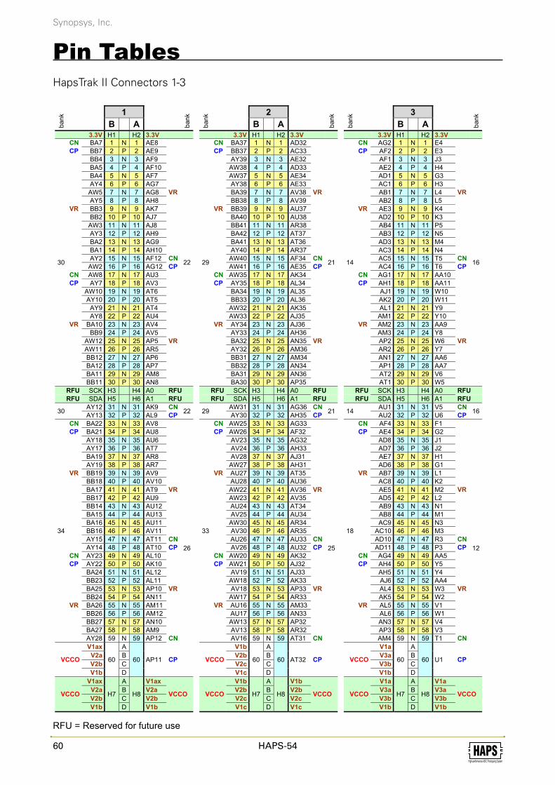
60 HAPS-54High-performance ASIC Prototyping System
Synopsys, Inc.
Pin TablesHapsTrak II Connectors 1-3
bank
1
bank
B A 3.3V H1 H2 3.3V
30
CN BA7 1 N 1 AE8
22
CP BB7 2 P 2 AE9 BB4 3 N 3 AF9 BA5 4 P 4 AF10 BA4 5 N 5 AF7 AY4 6 P 6 AG7 AW5 7 N 7 AG8 VR AY5 8 P 8 AH8 VR BB3 9 N 9 AK7 BB2 10 P 10 AJ7 AW3 11 N 11 AJ8 AY3 12 P 12 AH9 BA2 13 N 13 AG9 BA1 14 P 14 AH10 AY2 15 N 15 AF12 CN AW2 16 P 16 AG12 CP CN AW8 17 N 17 AU3 CP AY7 18 P 18 AV3 AW10 19 N 19 AT6 AY10 20 P 20 AT5 AY9 21 N 21 AT4 AY8 22 P 22 AU4 VR BA10 23 N 23 AV4 BB9 24 P 24 AV5 AW12 25 N 25 AP5 VR AW11 26 P 26 AR5 BB12 27 N 27 AP6 BA12 28 P 28 AP7 BA11 29 N 29 AM8 BB11 30 P 30 AN8
RFU SCK H3 H4 A0 RFU RFU SDA H5 H6 A1 RFU
30 AY12 31 N 31 AK9 CN 22 AY13 32 P 32 AL9 CP
34
CN BA22 33 N 33 AV8
26
CP BA21 34 P 34 AU8 AY18 35 N 35 AU6 AY17 36 P 36 AT7 BA19 37 N 37 AR8 AY19 38 P 38 AR7 VR BB19 39 N 39 AV9 BB18 40 P 40 AV10 BA17 41 N 41 AT9 VR BB17 42 P 42 AU9 BB14 43 N 43 AU12 BA15 44 P 44 AU13 BA16 45 N 45 AU11 BB16 46 P 46 AV11 AY15 47 N 47 AT11 CN AY14 48 P 48 AT10 CP CN AY23 49 N 49 AL10 CP AY22 50 P 50 AK10 BA24 51 N 51 AL12 BB23 52 P 52 AL11 BA25 53 N 53 AP10 VR BB24 54 P 54 AN11 VR BA26 55 N 55 AM11 BB26 56 P 56 AM12 BB27 57 N 57 AN10 BA27 58 P 58 AM9 AY28 59 N 59 AP12 CN
VCCO
V1ax
60
A
60 AP11 CP V2a B V2b C V1b D
VCCO
V1ax
H7
A
H8
V1ax
VCCO V2a B V2a V2b C V2b V1b D V1b
bank
2
bank
B A 3.3V H1 H2 3.3V
29
CN BA37 1 N 1 AD32
21
CP BB37 2 P 2 AC33 AY39 3 N 3 AE32 AW38 4 P 4 AD33 AW37 5 N 5 AE34 AY38 6 P 6 AE33 BA39 7 N 7 AV38 VR BB38 8 P 8 AV39 VR BB39 9 N 9 AU37 BA40 10 P 10 AU38 BB41 11 N 11 AR38 BA42 12 P 12 AT37 BA41 13 N 13 AT36 AY40 14 P 14 AR37 AW40 15 N 15 AF34 CN AW41 16 P 16 AE35 CPCN AW35 17 N 17 AK34 CP AY35 18 P 18 AL34 BA34 19 N 19 AL35 BB33 20 P 20 AL36 AW32 21 N 21 AK35 AW33 22 P 22 AJ35 VR AY34 23 N 23 AJ36 AY33 24 P 24 AH36 BA32 25 N 25 AN35 VR AY32 26 P 26 AM36 BB31 27 N 27 AM34 BB32 28 P 28 AN34 BA31 29 N 29 AN36 BA30 30 P 30 AP35
RFU SCK H3 H4 A0 RFU RFU SDA H5 H6 A1 RFU
29 AW31 31 N 31 AG36 CN 21 AY30 32 P 32 AH35 CP
33
CN AW25 33 N 33 AG33
25
CP AW26 34 P 34 AF32 AV23 35 N 35 AG32 AV24 36 P 36 AH33 AV28 37 N 37 AJ31 AW27 38 P 38 AH31 VR AU27 39 N 39 AT35 AU28 40 P 40 AU36 AW22 41 N 41 AV36 VR AW23 42 P 42 AV35 AU24 43 N 43 AT34 AV25 44 P 44 AU34 AW30 45 N 45 AR34 AV30 46 P 46 AR35 AU26 47 N 47 AU33 CN AV26 48 P 48 AU32 CPCN AW20 49 N 49 AK32 CP AW21 50 P 50 AJ32 AV19 51 N 51 AJ33 AW18 52 P 52 AK33 AV18 53 N 53 AP33 VR AW17 54 P 54 AR33 VR AU16 55 N 55 AM33 AU17 56 P 56 AN33 AW13 57 N 57 AP32 AV13 58 P 58 AR32 AV16 59 N 59 AT31 CN
VCCO
V1b
60
A
60 AT32 CPV2b BV2c CV1c D
VCCO
V1b
H7
A
H8
V1b
VCCO V2b B V2b V2c C V2c V1c D V1c
bank
3
bank
B A 3.3V H1 H2 3.3V
14
CN AG2 1 N 1 E4
16
CP AF2 2 P 2 E3 AF1 3 N 3 J3 AE2 4 P 4 H4 AD1 5 N 5 G3 AC1 6 P 6 H3 AB1 7 N 7 L4 VR AB2 8 P 8 L5 VR AE3 9 N 9 K4 AD2 10 P 10 K3 AB4 11 N 11 P5 AB3 12 P 12 N5 AD3 13 N 13 M4 AC3 14 P 14 N4 AC5 15 N 15 T5 CN AC4 16 P 16 T6 CPCN AG1 17 N 17 AA10 CP AH1 18 P 18 AA11 AJ1 19 N 19 W10 AK2 20 P 20 W11 AL1 21 N 21 Y9 AM1 22 P 22 Y10 VR AM2 23 N 23 AA9 AM3 24 P 24 Y8 AP2 25 N 25 W6 VR AR2 26 P 26 Y7 AN1 27 N 27 AA6 AP1 28 P 28 AA7 AT2 29 N 29 V6 AT1 30 P 30 W5
RFU SCK H3 H4 A0 RFU RFU SDA H5 H6 A1 RFU
14 AU1 31 N 31 V5 CN 16 AU2 32 P 32 U6 CP
18
CN AF4 33 N 33 F1
12
CP AE4 34 P 34 G2 AD8 35 N 35 J1 AD7 36 P 36 J2 AE7 37 N 37 H1 AD6 38 P 38 G1 VR AB7 39 N 39 L1 AC8 40 P 40 K2 AE5 41 N 41 M2 VR AD5 42 P 42 L2 AB9 43 N 43 N1 AB8 44 P 44 M1 AC9 45 N 45 N3 AC10 46 P 46 M3 AD10 47 N 47 R3 CN AD11 48 P 48 P3 CPCN AG4 49 N 49 AA5 CP AH4 50 P 50 Y5 AH5 51 N 51 Y4 AJ6 52 P 52 AA4 AL4 53 N 53 W3 VR AK5 54 P 54 W2 VR AL5 55 N 55 V1 AL6 56 P 56 W1 AN3 57 N 57 V4 AP3 58 P 58 V3 AM4 59 N 59 T1 CN
VCCO
V1a
60
A
60 U1 CPV3a BV3b CV1b D
VCCO
V1a
H7
A
H8
V1a
VCCO V3a B V3a V3b C V3b V1b D V1b
RFU = Reserved for future use

61HAPS-54High-performance ASIC Prototyping System
Synopsys, Inc.
HapsTrak II Connectors 4-6
bank
4
bank
B A 3.3V H1 H2 3.3V
13
CN AB38 1 N 1 G39
15
CP AB37 2 P 2 G38 AJ40 3 N 3 F40 AH40 4 P 4 F39 AJ41 5 N 5 E40 AJ42 6 P 6 E39 AH41 7 N 7 R38 VR AG42 8 P 8 R39 VR AG41 9 N 9 P37 AF40 10 P 10 R37 AF42 11 N 11 N38 AF41 12 P 12 P38 AD41 13 N 13 M39 AE42 14 P 14 N39 AD42 15 N 15 L39 CN AC41 16 P 16 M38 CP CN AC39 17 N 17 W37 CP AC40 18 P 18 W36 AK42 19 N 19 W35 AL41 20 P 20 Y35 AN41 21 N 21 Y34 AM41 22 P 22 AA34 VR AM42 23 N 23 AA36 AL42 24 P 24 AA35 AP41 25 N 25 U39 VR AP42 26 P 26 T39 AT42 27 N 27 W38 AR42 28 P 28 V39 AU41 29 N 29 U38 AT41 30 P 30 T37
RFU SCK H3 H4 A0 RFU RFU SDA H5 H6 A1 RFU
13 AV41 31 N 31 K39 CN 15 AU42 32 P 32 K40 CP
17
CN AP40 33 N 33 G41
11
CP AN40 34 P 34 F41 AF37 35 N 35 J41 AG37 36 P 36 H41 AG38 37 N 37 K42 AF39 38 P 38 J42 VR AD38 39 N 39 M41 AE37 40 P 40 L42 AE38 41 N 41 L41 VR AE39 42 P 42 L40 AD37 43 N 43 N41 AD36 44 P 44 M42 AD35 45 N 45 P40 AC36 46 P 46 N40 AB36 47 N 47 Y40 CN AC35 48 P 48 W40 CP CN AR39 49 N 49 W41 CP AT39 50 P 50 V40 AK39 51 N 51 V41 AJ38 52 P 52 U42 AH38 53 N 53 T41 VR AJ37 54 P 54 T40 VR AK37 55 N 55 U41 AK38 56 P 56 T42 AM39 57 N 57 R40 AL39 58 P 58 P41 AP38 59 N 59 AA37 CN
VCCO
V1b
60
A
60 Y37 CP V3b B V3c C V1c D
VCCO
V1b
H7
A
H8
V1b
VCCO V3b B V3b V3c C V3c V1c D V1c
bank
5
bank
B A 3.3V H1 H2 3.3V
24
CN G13 1 N 1 A26
32
CP H13 2 P 2 B27 J11 3 N 3 C28 J10 4 P 4 C29 J12 5 N 5 A27 K12 6 P 6 B28 L10 7 N 7 A25 VR L11 8 P 8 B24 VR K10 9 N 9 C25 L9 10 P 10 C24 M11 11 N 11 A24 N11 12 P 12 B23 L12 13 N 13 B26 M12 14 P 14 C26 N10 15 N 15 B22 CN P10 16 P 16 C23 CPCN G11 17 N 17 B14 CP F12 18 P 18 B13 H10 19 N 19 C15 H9 20 P 20 C14 G9 21 N 21 C16 F9 22 P 22 B16 VR E9 23 N 23 A15 E10 24 P 24 A14 J8 25 N 25 A17 VR H8 26 P 26 A16 K9 27 N 27 B18 K8 28 P 28 B17 E8 29 N 29 C19 E7 30 P 30 C18
RFU SCK H3 H4 A0 RFU RFU SDA H5 H6 A1 RFU
24 G8 31 N 31 A22 CN 32 F7 32 P 32 A21 CP
20
CN N9 33 N 33 C11
28
CP P8 34 P 34 B11 L6 35 N 35 A12 L7 36 P 36 B12 M6 37 N 37 D12 M7 38 P 38 D11 VR K7 39 N 39 A10 J7 40 P 40 A11 J6 41 N 41 D8 VR K5 42 P 42 C9 H5 43 N 43 D10 J5 44 P 44 C10 H6 45 N 45 B9 G7 46 P 46 A9 E5 47 N 47 B8 CN F5 48 P 48 C8 CPCN P6 49 N 49 B1 CP N6 50 P 50 C1 T9 51 N 51 C3 R9 52 P 52 B3 T7 53 N 53 D5 VR U7 54 P 54 C5 VR R8 55 N 55 C4 R7 56 P 56 D3 U9 57 N 57 A4 U8 58 P 58 B4 T11 59 N 59 B7 CN
VCCO
V2a
60
A
60 A7 CPV3ax BV3b CV2b D
VCCO
V2a
H7
A
H8
V2a
VCCO V3ax B V3ax V3b C V3b V2b D V2b
bank
6
bank
B A 3.3V H1 H2 3.3V
23
CN E35 1 N 1 F14
31
CP F35 2 P 2 E15 J31 3 N 3 D17 H31 4 P 4 D16 G31 5 N 5 F15 G32 6 P 6 F16 H33 7 N 7 E17 VR G33 8 P 8 F17 VR G34 9 N 9 F20 H34 10 P 10 E20 P31 11 N 11 E18 N31 12 P 12 D18 M31 13 N 13 F19 M32 14 P 14 E19 M33 15 N 15 D23 CN M34 16 P 16 D22 CPCN E33 17 N 17 E30 CP E32 18 P 18 D30 J33 19 N 19 F29 K33 20 P 20 F30 L31 21 N 21 D28 L32 22 P 22 D27 VR J32 23 N 23 E28 K32 24 P 24 E29 P32 25 N 25 E27 VR P33 26 P 26 F27 R32 27 N 27 F25 R33 28 P 28 F26 U32 29 N 29 E25 T32 30 P 30 E24
RFU SCK H3 H4 A0 RFU RFU SDA H5 H6 A1 RFU
23 T31 31 N 31 F24 CN 31 U31 32 P 32 E23 CP
19
CN T35 33 N 33 C30
27
CP U34 34 P 34 B31 J37 35 N 35 A31 K37 36 P 36 A30 J36 37 N 37 B32 H35 38 P 38 A32 VR L35 39 N 39 D33 L36 40 P 40 D32 J35 41 N 41 C33 VR K35 42 P 42 B33 P36 43 N 43 B34 N36 44 P 44 C34 M37 45 N 45 A35 L37 46 P 46 A34 M36 47 N 47 D36 CN N35 48 P 48 D35 CPCN V36 49 N 49 C41 CP U36 50 P 50 B42 G36 51 N 51 B41 F36 52 P 52 A41 D37 53 N 53 B38 VR E38 54 P 54 B39 VR E37 55 N 55 A40 F37 56 P 56 A39 V34 57 N 57 C40 V35 58 P 58 C39 W33 59 N 59 B36 CN
VCCO
V2b
60
A
60 B37 CPV3b BV3cx CV2c D
VCCO
V2b
H7
A
H8
V2b
VCCO V3b B V3b V3cx C V3cx V2c D V2c
RFU = Reserved for future use

62 HAPS-54High-performance ASIC Prototyping System
Synopsys, Inc.
HapsTrak II Connector 7
bank
7
bank
B A 3.3V H1 H2 3.3V
6
CN AR29 1 N 1 H14
5
CP AR28 2 P 2 G14 AT15 3 N 3 G16 AT14 4 P 4 H16 AM17 5 N 5 J15 AM18 6 P 6 H15 AM19 7 N 7 J16 AL19 8 P 8 J17 AL17 9 N 9 L17 AK18 10 P 10 M17 AJ18 11 N 11 H18 7 AK19 12 P 12 J18
8 AL20 13 N 13 N19 5 AK20 14 P 14 N18
6
AP17 15 N 15 J23 CN
7
AN18 16 P 16 J22 CP CN AR30 17 N 17 J20 CP AT30 18 P 18 K20
8
AN20 19 N 19 N20 AP20 20 P 20 P20 AT21 21 N 21 L21 AT20 22 P 22 L20
6 AP18 23 N 23 N21 AN19 24 P 24 P21
8
AJ20 25 N 25 M21 AJ21 26 P 26 N22 AT19 27 N 27 H21 AR20 28 P 28 J21 AL21 29 N 29 P22 AM21 30 P 30 P23
RFU SCK H3 H4 A0 RFU RFU SDA H5 H6 A1 RFU
8
AK22 31 N 31 F22 CN
7
AK23 32 P 32 G22 CP CN AT24 33 N 33 M22 CP AT25 34 P 34 L22
6 AK24 35 N 35 K23 AJ25 36 P 36 K22
8
AN24 37 N 37 G24 AP23 38 P 38 H24 AN23 39 N 39 G23 AM23 40 P 40 H23
6
AM24 41 N 41 J25 AL25 42 P 42 H25 AK25 43 N 43 L24
5
AL24 44 P 44 L25
8 AR25 45 N 45 K24 AP25 46 P 46 K25
6 AN25 47 N 47 N25 CN AN26 48 P 48 P25 CP
8 CN AR24 49 N 49 H28 CP AR23 50 P 50 G27
6 AR27 51 N 51 L26 AP26 52 P 52 M26
8 AT26 53 N 53 H26 7 AT27 54 P 54 G26
6
AP27 55 N 55 K27
5
AP28 56 P 56 J28 AT29 57 N 57 G29 AU29 58 P 58 G28
8 AM22 59 N 59 J27 CN
VCCO 2.5V 60
A
60 J26 CP B C D
VCCO 2.5V H7
A
H8 2.5V VCCO B C D
Note Connectors A7, B7, C7 and D7 are HapsTrak II connectors for boards with serial number 070647 and above. Previous versions had HapsTrak I connectors!
Note The VREF pins in connector 7 are not connected to the same pins as other HapsTrak connectors!
RFU = Reserved for future use

63HAPS-54High-performance ASIC Prototyping System
Synopsys, Inc.
Inter-FPGA Connections A-B (fast)
bank
A – B 2.5V
bank
A B
1
R28 1 P 1 R28
1 R27 2 N 2 R27 M13 3 P 3 M13 N13 4 N 4 N13
2
CP AH16 5 P 5 AH16 CP
2
CN AJ15 6 N 6 AJ15 CNCP AH30 7 P 7 AH30 CPCN AH29 8 N 8 AH29 CN
AJ16 9 P 9 AJ16 AJ17 10 N 10 AJ17 AK30 11 P 11 AK30 AJ30 12 N 12 AJ30
7
M23 13 P 13 M23
7
N23 14 N 14 N23 G21 15 P 15 G21 H20 16 N 16 H20 H19 17 P 17 H19 G19 18 N 18 G19
5
M24 19 P 19 M24
5
N24 20 N 20 N24 CP K19 21 P 21 K19 CPCN L19 22 N 22 L19 CNCP M18 23 P 23 M18 CPCN M19 24 N 24 M19 CN
R18 25 P 25 R18 P18 26 N 26 P18 H29 27 P 27 H29 H30 28 N 28 H30
6
AL26 29 P 29 AL26
6
AM26 30 N 30 AM26 AR15 31 P 31 AR15 AP15 32 N 32 AP15
CP AR13 33 P 33 AR13 CPCN AR14 34 N 34 AR14 CN
8
AJ23 35 P 35 AJ23
8
AJ22 36 N 36 AJ22 CP AN21 37 P 37 AN21 CPCN AP21 38 N 38 AP21 CNCP AR18 39 P 39 AR18 CPCN AR19 40 N 40 AR19 CN
AL22 41 41 AL22 AU21 42 P 42 AU21 AT22 43 N 43 AT22 AR22 44 P 44 AR22 AP22 45 N 45 AP22
bank
A – B V2a
bank
A B
32
A29 46 P 46 BA29
34
B29 47 N 47 AY29 CP C21 48 P 48 BA20 CPCN C20 49 N 49 AY20 CNCP A20 50 P 50 BB21 CPCN B21 51 N 51 BB22 CN
28
C13 52 P 52 AJ12
26 D13 53 N 53 AK12 CP B6 54 P 54 AV6 CN C6 55 N 55 AU7 CP D7 56 P 56 AW7 CP 30CN D6 57 N 57 AW6 CN
A2 58 P 58 AK8 CP 22 B2 59 N 59 AL7 CN D1 60 P 60 AV1 30 D2 61 N 61 AW1
24
P12 62 P 62 BB29 34 P11 63 N 63 BB28 CP H11 64 P 64 AR12 CP 26CN G12 65 N 65 AT12 CNCP E12 66 P 66 BB13 34CN E13 67 N 67 BA14
20
G6 68 P 68 BB6 CP 30 F6 69 N 69 BA6 CNCP M8 70 P 70 AJ10
26CN M9 71 N 71 AJ11 CP P7 72 P 72 AR9 CPCN N8 73 N 73 AR10 CN
U11 74 74 AY27 34 V9 75 P 75 AF11
22 V8 76 N 76 AE10 V11 77 P 77 AH11 CP V10 78 N 78 AG11 CN
bank
A – B V2b
bank
A B
31
E14 79 P 79 AU14
33
D15 80 N 80 AV14 CP D21 81 P 81 AW15 CN D20 82 N 82 AV15 CP F21 83 P 83 AV21 CPCN E22 84 N 84 AV20 CN
27
D31 85 P 85 AU23 CP C31 86 N 86 AU22 CN
CP C36 87 P 87 AL32 25CN C35 88 N 88 AM32 CP A37 89 P 89 AB33 21CN A36 90 N 90 AB32
D40 91 P 91 AY37 CP
29 D41 92 N 92 AW36 CN E42 93 P 93 AY42 D42 94 N 94 AW42
23
N33 95 P 95 AV33 CP 25 N34 96 N 96 AV34 CNCP E34 97 P 97 AH34 CP 21CN F34 98 N 98 AG34 CNCP F31 99 P 99 AV31 CP 25CN F32 100 N 100 AU31 CN
19
R34 101 P 101 AF35 CP 21 P35 102 N 102 AF36 CNCP T34 103 P 103 AL31 25CN U33 104 N 104 AM31 CP R35 105 P 105 BB36 CP 29CN T36 106 N 106 BA36 CN
V33 107 107 AW16 33 Y33 108 P 108 AV29
W32 109 N 109 AW28 Y32 110 P 110 AG31 25 AA32 111 N 111 AF31
Inter-FPGA Connections A-B (slow)
A – B
bank
V1axA V3a
B bank
22
AF11 112 G4
16
AE10 113 F4 AH11 114 R5 AG11 115 R4
AK8 116 U4 AL7 117 T4
26
AV6 118 E2
12
AU7 119 F2 AR9 120 P2
AR10 121 P1 AR12 122 R2 AT12 123 T2 AJ10 124 AA1 AJ11 125 AA2 AJ12 126 Y2 AK12 127 Y3
30
AV1 128 AB6
14
AW1 129 AC6 AW7 130 AG3 AW6 131 AH3 BB6 132 AJ2 BA6 133 AJ3
34
BB13 134 AB11
18
BA14 135 AC11 BB21 136 AF6 BB22 137 AF5 BA20 138 AG6 AY20 139 AH6
A – B
bank
V1a A V3ax
B bank
16
G4 140 A29
32
F4 141 B29 R5 142 C21 R4 143 C20 U4 144 A20 T4 145 B21
12
E2 146 C13
28
F2 147 D13 P2 148 B6 P1 149 C6 R2 150 D7 T2 151 D6
AA1 152 A2 AA2 153 B2
Y2 154 D1 Y3 155 D2
14
AB6 156 P12
24
AC6 157 P11 AG3 158 H11 AH3 159 G12 AJ2 160 E12 AJ3 161 E13
18
AB11 162 G6
20
AC11 163 F6 AF6 164 M8 AF5 165 M9 AG6 166 P7 AH6 167 N8
NoteThe inter-FPGA signals with level shifters all have strong pull-up resistors. Internal pull-down don’t work for these signals.

64 HAPS-54High-performance ASIC Prototyping System
Synopsys, Inc.
Inter-FPGA Connections D-C (fast)
bank
D – C 2.5V
bank
D C
1
R28 1 P 1 R28
1 R27 2 N 2 R27 M13 3 P 3 M13 N13 4 N 4 N13
2
CP AH16 5 P 5 AH16 CP
2
CN AJ15 6 N 6 AJ15 CNCP AH30 7 P 7 AH30 CPCN AH29 8 N 8 AH29 CN
AJ16 9 P 9 AJ16 AJ17 10 N 10 AJ17 AK30 11 P 11 AK30 AJ30 12 N 12 AJ30
7
M23 13 P 13 M23
7
N23 14 N 14 N23 G21 15 P 15 G21 H20 16 N 16 H20 H19 17 P 17 H19 G19 18 N 18 G19
5
M24 19 P 19 M24
5
N24 20 N 20 N24 CP K19 21 P 21 K19 CPCN L19 22 N 22 L19 CNCP M18 23 P 23 M18 CPCN M19 24 N 24 M19 CN
R18 25 P 25 R18 P18 26 N 26 P18 H29 27 P 27 H29 H30 28 N 28 H30
6
AL26 29 P 29 AL26
6
AM26 30 N 30 AM26 AR15 31 P 31 AR15 AP15 32 N 32 AP15
CP AR13 33 P 33 AR13 CPCN AR14 34 N 34 AR14 CN
8
AJ23 35 P 35 AJ23
8
AJ22 36 N 36 AJ22 CP AN21 37 P 37 AN21 CPCN AP21 38 N 38 AP21 CNCP AR18 39 P 39 AR18 CPCN AR19 40 N 40 AR19 CN
AL22 41 41 AL22 AU21 42 P 42 AU21 AT22 43 N 43 AT22 AR22 44 P 44 AR22 AP22 45 N 45 AP22
bank
D – C V2b
bank
D C
32
A29 46 P 46 BA29
34
B29 47 N 47 AY29 CP C21 48 P 48 BA20 CPCN C20 49 N 49 AY20 CNCP A20 50 P 50 BB21 CPCN B21 51 N 51 BB22 CN
28
C13 52 P 52 AJ12
26 D13 53 N 53 AK12 CP B6 54 P 54 AV6 CN C6 55 N 55 AU7 CP D7 56 P 56 AW7 CP 30CN D6 57 N 57 AW6 CN
A2 58 P 58 AK8 CP 22 B2 59 N 59 AL7 CN D1 60 P 60 AV1 30 D2 61 N 61 AW1
24
P12 62 P 62 BB29 34 P11 63 N 63 BB28 CP H11 64 P 64 AR12 CP 26CN G12 65 N 65 AT12 CNCP E12 66 P 66 BB13 34CN E13 67 N 67 BA14
20
G6 68 P 68 BB6 CP 30 F6 69 N 69 BA6 CNCP M8 70 P 70 AJ10
26CN M9 71 N 71 AJ11 CP P7 72 P 72 AR9 CPCN N8 73 N 73 AR10 CN
U11 74 74 AY27 34 V9 75 P 75 AF11
22 V8 76 N 76 AE10 V11 77 P 77 AH11 CP V10 78 N 78 AG11 CN
bank
D – C V2c
bank
D C
31
E14 79 P 79 AU14
33
D15 80 N 80 AV14 CP D21 81 P 81 AW15 CN D20 82 N 82 AV15 CP F21 83 P 83 AV21 CPCN E22 84 N 84 AV20 CN
27
D31 85 P 85 AU23 CP C31 86 N 86 AU22 CN
CP C36 87 P 87 AL32 25CN C35 88 N 88 AM32 CP A37 89 P 89 AB33 21CN A36 90 N 90 AB32
D40 91 P 91 AY37 CP
29 D41 92 N 92 AW36 CN E42 93 P 93 AY42 D42 94 N 94 AW42
23
N33 95 P 95 AV33 CP 25 N34 96 N 96 AV34 CNCP E34 97 P 97 AH34 CP 21CN F34 98 N 98 AG34 CNCP F31 99 P 99 AV31 CP 25CN F32 100 N 100 AU31 CN
19
R34 101 P 101 AF35 CP 21 P35 102 N 102 AF36 CNCP T34 103 P 103 AL31 25CN U33 104 N 104 AM31 CP R35 105 P 105 BB36 CP 29CN T36 106 N 106 BA36 CN
V33 107 107 AW16 33 Y33 108 P 108 AV29
W32 109 N 109 AW28 Y32 110 P 110 AG31 25 AA32 111 N 111 AF31
Inter-FPGA Connections D-C (slow)
D – C
bank
V1cxD V3c
C bank
21
AB33 112 H38
15
AB32 113 H39 AF35 114 K38 AF36 115 J38 AH34 116 H40 AG34 117 J40
25
AG31 118 F42
11
AF31 119 G42 AV33 120 AA40 AV34 121 AA39 AV31 122 Y39 AU31 123 Y38 AL32 124 W42
AM32 125 Y42 AL31 126 AA42
AM31 127 AA41
29
AY42 128 AB41
13
AW42 129 AB42 AY37 130 AB39 AW36 131 AC38 BB36 132 AE40 BA36 133 AD40
33
AV29 134 AB34
17
AW28 135 AC34 AU23 136 AR40 AU22 137 AT40 AV21 138 AV40 AV20 139 AU39
D – C
bank
V1c D V3cx
C bank
15
H38 140 E14
31
H39 141 D15 K38 142 D21 J38 143 D20 H40 144 F21 J40 145 E22
11
F42 146 D31
27
G42 147 C31 AA40 148 C36 AA39 149 C35
Y39 150 A37 Y38 151 A36
W42 152 D40 Y42 153 D41
AA42 154 E42 AA41 155 D42
13
AB41 156 N33
23
AB42 157 N34 AB39 158 E34 AC38 159 F34 AE40 160 F31 AD40 161 F32
17
AB34 162 R34
19
AC34 163 P35 AR40 164 T34 AT40 165 U33 AV40 166 R35 AU39 167 T36
NoteThe inter-FPGA signals with level shifters all have strong pull-up resistors. Internal pull-down don’t work for these signals.

65HAPS-54High-performance ASIC Prototyping System
Synopsys, Inc.
Inter-FPGA Connections A-D (fast)
bank
A – D V1b
bank
A D
15
H38 1 P 1 G4
16
H39 2 N 2 F4 CP K38 3 P 3 R5 CPCN J38 4 N 4 R4 CNCP H40 5 P 5 U4 CPCN J40 6 N 6 T4 CN
11
F42 7 P 7 E2
12
G42 8 N 8 F2 CP AA40 9 P 9 P2 CPCN AA39 10 N 10 P1 CNCP Y39 11 P 11 R2 CPCN Y38 12 N 12 T2 CN
W42 13 P 13 AA1 Y42 14 N 14 AA2 AA42 15 P 15 Y2 AA41 16 N 16 Y3
13
AB41 17 P 17 AB6
14
AB42 18 N 18 AC6 CP AB39 19 P 19 AG3 CPCN AC38 20 N 20 AH3 CNCP AE40 21 P 21 AJ2 CPCN AD40 22 N 22 AJ3 CN
17
AB34 23 P 23 AB11
18
AC34 24 N 24 AC11 CP AR40 25 P 25 AF6 CPCN AT40 26 N 26 AF5 CNCP AV40 27 P 27 AG6 CPCN AU39 28 N 28 AH6 CN
AN39 29 29 AN4 AN38 30 P 30 AR3 AM38 31 N 31 AR4 AM37 32 P 32 AM6 AL37 33 N 33 AN5
bank
A – D V1b
bank
A D
21
AB33 34 P 34 AF11
22
AB32 35 N 35 AE10 CP AF35 36 P 36 AH11 CPCN AF36 37 N 37 AG11 CNCP AH34 38 P 38 AK8 CPCN AG34 39 N 39 AL7 CN
25
AG31 40 P 40 AV6
26
AF31 41 N 41 AU7 CP AV33 42 P 42 AR9 CPCN AV34 43 N 43 AR10 CNCP AV31 44 P 44 AR12 CPCN AU31 45 N 45 AT12 CN
AL32 46 P 46 AJ10 AM32 47 N 47 AJ11 AL31 48 P 48 AJ12 AM31 49 N 49 AK12
29
AY42 50 P 50 AV1
30
AW42 51 N 51 AW1 CP AY37 52 P 52 AW7 CPCN AW36 53 N 53 AW6 CNCP BB36 54 P 54 BB6 CPCN BA36 55 N 55 BA6 CN
33
AV29 56 P 56 BB13
34
AW28 57 N 57 BA14 CP AU23 58 P 58 BB21 CPCN AU22 59 N 59 BB22 CNCP AV21 60 P 60 BA20 CPCN AV20 61 N 61 AY20 CN
AW16 62 62 AY27 AU14 63 P 63 BB29 AV14 64 N 64 BB28 AW15 65 P 65 BA29 AV15 66 N 66 AY29

66 HAPS-54High-performance ASIC Prototyping System
Synopsys, Inc.
Inter-FPGA Connections B-C (fast)
bank
B – C V3b
bank
B C
31
E14 1 P 1 A29
32
D15 2 N 2 B29 CP D21 3 P 3 C21 CPCN D20 4 N 4 C20 CNCP F21 5 P 5 A20 CPCN E22 6 N 6 B21 CN
27
D31 7 P 7 C13
28
C31 8 N 8 D13 CP C36 9 P 9 B6 CPCN C35 10 N 10 C6 CNCP A37 11 P 11 D7 CPCN A36 12 N 12 D6 CN
D40 13 P 13 A2 D41 14 N 14 B2 E42 15 P 15 D1 D42 16 N 16 D2
23
N33 17 P 17 P12
24
N34 18 N 18 P11 CP E34 19 P 19 H11 CPCN F34 20 N 20 G12 CNCP F31 21 P 21 E12 CPCN F32 22 N 22 E13 CN
19
R34 23 P 23 G6
20
P35 24 N 24 F6 CP T34 25 P 25 M8 CPCN U33 26 N 26 M9 CNCP R35 27 P 27 P7 CPCN T36 28 N 28 N8 CN
V33 29 29 U11 Y33 30 P 30 V9 W32 31 N 31 V8 Y32 32 P 32 V11 AA32 33 N 33 V10
bank
B – C V3b
bank
B C
15
H38 34 P 34 G4
16
H39 35 N 35 F4 CP K38 36 P 36 R5 CPCN J38 37 N 37 R4 CNCP H40 38 P 38 U4 CPCN J40 39 N 39 T4 CN
11
F42 40 P 40 E2
12
G42 41 N 41 F2 CP AA40 42 P 42 P2 CPCN AA39 43 N 43 P1 CNCP Y39 44 P 44 R2 CPCN Y38 45 N 45 T2 CN
W42 46 P 46 AA1 Y42 47 N 47 AA2 AA42 48 P 48 Y2 AA41 49 N 49 Y3
13
AB41 50 P 50 AB6
14
AB42 51 N 51 AC6 CP AB39 52 P 52 AG3 CPCN AC38 53 N 53 AH3 CNCP AE40 54 P 54 AJ2 CPCN AD40 55 N 55 AJ3 CN
17
AB34 56 P 56 AB11
18
AC34 57 N 57 AC11 CP AR40 58 P 58 AF6 CPCN AT40 59 N 59 AF5 CNCP AV40 60 P 60 AG6 CPCN AU39 61 N 61 AH6 CN
AN39 62 62 AN4 AN38 63 P 63 AR3 AM38 64 N 64 AR4 AM37 65 P 65 AM6 AL37 66 N 66 AN5

67HAPS-54High-performance ASIC Prototyping System
Synopsys, Inc.
HapsTrak CDE In
CDE In
2.5V
bank pin B A pin bank
1
R15 D16 1 1 D0 AJ27
2
P16 D17 2 2 D1 AJ26 N30 D18 3 3 D2 AL14 P30 D19 4 4 D3 AL15 P13 D20 5 5 D4 AK29 N14 D21 6 6 D5 AJ28 M29 D22 7 7 D6 AK13 N29 D23 8 8 D7 AJ13 P15 D24 9 9 D8 AM16
4
N15 D25 10 10 D9 AN16 P28 D26 11 11 D10 AN30 N28 D27 12 12 D11 AM29R17 D28 13 13 D12 AK17 P17 D29 14 14 D13 AL16 P26 D30 15 15 D14 AK27 P27 D31 16 16 D15 AK28
0 R30 RDWR 17 17 BUSY AH15 0 T30 CS 18 18 CCLK AF15 TMS 19 19 CDE_IN_1 TCK 20 20 CDE_IN_2 TDI 21 21 CDE_IN_3 TDO 22 22 CDE_IN_4 2.5V 23 23 Reserved_1 GND 24 24 Reserved_2 ALL_DONE 25 25 Reserved_3 BOARD_INIT_B 26 26 Reserved_4 BOARD_PROG_B 27 27 Reserved_5 Reserved_8 28 28 Reserved_6 Reserved_9 29 29 Reserved_7 2.5V 30 30 (No Connect)
NoteThe signals connected to the FPGAs are all terminated to 1.25V with 100 Ohm resistors. Internal pull-up/pull-down resistors don’t work for these signals.
HapsTrak CDE Out
CDE Out
2.5V B A B_D16 1 1 B_D0 B_D17 2 2 B_D1 B_D18 3 3 B_D2 B_D19 4 4 B_D3 B_D20 5 5 B_D4 B_D21 6 6 B_D5 B_D22 7 7 B_D6 B_D23 8 8 B_D7 B_D24 9 9 B_D8 B_D25 10 10 B_D9 B_D26 11 11 B_D10 B_D27 12 12 B_D11 B_D28 13 13 B_D12 B_D29 14 14 B_D13 B_D30 15 15 B_D14 B_D31 16 16 B_D15 B_RDWR 17 17 B_BUSY B_CS 18 18 B_CCLK TMS_O 19 19 CDE_OUT_1 TCK_O 20 20 CDE_OUT_2 TDI_O 21 21 CDE_OUT_3 TDO_O 22 22 CDE_OUT_4 VCONF 23 23 Reserved_1 CHAINED_n 24 24 Reserved_2 ALL_DONE 25 25 Reserved_3 BOARD_INIT_B 26 26 Reserved_4 BOARD_PROG_B 27 27 Reserved_5 Reserved_8 28 28 Reserved_6 Reserved_9 29 29 Reserved_7 (No Connect) 30 30 2.5V

68 HAPS-54High-performance ASIC Prototyping System
Synopsys, Inc.
Global ClocksGlobal Clocks
Source Destination From MMCX Outputs from FPGAs To MMCX Inputs to FPGAs
2.5V 2.5V External Internal pin / bank External Internal P/N pin / bank
GCLK_IN1
A_GCLKO(1) B_GCLKO(1) C_GCLKO(1) D_GCLKO(1)
AN29
4
GCLK_OUT1a GCLK_OUT1b GCLK(1) P AP30
4
GCLK_IN2
A_GCLKO(2) B_GCLKO(2) C_GCLKO(2) D_GCLKO(2)
AM14 GCLK_OUT2a GCLK_OUT2b GCLK(2) P AM13
GCLK_IN3
A_GCLKO(3) B_GCLKO(3) C_GCLKO(3) D_GCLKO(3)
AN28 GCLK_OUT3a GCLK_OUT3b GCLK(3) P AM28
GCLK_IN4
A_GCLKO(4) B_GCLKO(4) C_GCLKO(4) D_GCLKO(4)
AM27 GCLK_OUT4a GCLK_OUT4b GCLK(4) P AL27
GCLK_IN5
A_GCLKO(5) B_GCLKO(5) C_GCLKO(5) D_GCLKO(5)
AN13 GCLK_OUT5a GCLK_OUT5b GCLK(5) P AP13
GCLK_IN6
A_GCLKO(6) B_GCLKO(6) C_GCLKO(6) D_GCLKO(6)
L16
3
GCLK_OUT6a GCLK_OUT6b GCLK(6) P K28
3
GCLK_IN7
A_GCLKO(7) B_GCLKO(7) C_GCLKO(7) D_GCLKO(7)
K29 GCLK_OUT7a GCLK_OUT7b GCLK(7) P M14
GCLK_IN8
A_GCLKO(8) B_GCLKO(8) C_GCLKO(8) D_GCLKO(8)
AL29
2
GCLK_OUT8a GCLK_OUT8b GCLK(8) P N16
GCLK_IN9
A_GCLKO(9) B_GCLKO(9) C_GCLKO(9) D_GCLKO(9)
AL30 GCLK_OUT9a GCLK_OUT9b GCLK(9) P L29
PLL_DP PLL_DN
A_PLL_D B_PLL_D C_PLL_D D_PLL_D
J13 3
GCLK_OUT_D1P GCLK(10) P K15
3 GCLK_OUT_D1N GCLK(11) N K14GCLK_OUT_D2P GCLK(12) P M27GCLK_OUT_D2N GCLK(13) N N26
PLL_SE
A_PLL_SE B_PLL_SE C_PLL_SE D_PLL_SE
M28 3
GCLK_OUT_SE1 GCLK_OUT_SE2 GCLK(14) P K13
3 GCLK_OUT_SE3 GCLK_OUT_SE4 GCLK(15) P L27
GCLK_OUT_SE5 GCLK(16) P L15GCLK_OUT_SE6
Note The signals driving the internal source are parallel terminated and should not be left undriven. Use LVCMOS drivers for these signals. Do not use DCI.
Direct Differential Clocks RESETDirect Clocks
pin 2.5V N P bank
GC_A1 GC_B1 GC_C1 GC_D1 AN14 AN15 4 GC_A2 GC_B2 GC_C2 GC_D2 K30 J30 3
RESET 2.5V pin bank
A_RESET_n B_RESET_n L14 3
C_RESET_n D_RESET_n
GPIO GPIO
A B C D
pin bank V pin bank V pin bank V pin bank V1 AY27
34 V1ax
AN4
18 V3a
AN39
17 V3c
AW16
33 V1cx
LEDs A, B, C, D : Green 2 BB29 AR3 AN38 AU14 3 BB28 AR4 AM38 AV14 4 BA29 AM6 AM37 AW15 5 AY29 AN5 AL37 AV15 6 AN4
18 V1a
U11
20 V3ax
V33
19 V3cx
AN39
17 V1c
LEDs A, B, C, D : Red 7 AR3 V9 Y33 AN38 8 AR4 V8 W32 AM38 9 AM6 V11 Y32 AM37
10 AN5 V10 AA32 AL37

69HAPS-54High-performance ASIC Prototyping System
Synopsys, Inc.
Signal Delays
Connectors to FPGAs
Average delay in pico-seconds from
connectors to FPGAs
FPGA A FPGA B FPGA C FPGA D Delay +/- Delay +/- Delay +/- Delay +/-
1 724 2 724 2 724 2 724 2 2 721 4 721 4 721 4 721 4 3 356 4 356 4 356 4 356 4 4 293 1 293 1 293 1 293 1 5 694 3 694 3 694 3 694 3 6 710 2 710 2 710 2 710 2 7 490 3 507 4 507 4 490 3
FPGA to FPGA
Average delay in pico-seconds from
FPGA to FPGA
A – B D – C A – D B – C Pin Delay +/- Delay +/- Delay +/- Delay +/- 1 – 66 – – – – 1 199 3 1 199 3 1 – 111 1 197 1 1 197 1 – – – – * 112 – 167 2 787 2 2 787 2 – – – – Global signals
1 – 119 1 197 1 1 197 1 – – – –
* The delay of the transmission gate must be added. This delay depends on the voltage translation. The performance is optimal when the voltage is the same on both sides.

70 HAPS-54High-performance ASIC Prototyping System
Synopsys, Inc.
Layout
A1
V1ax
A3V1a
A2
V1b
A4
V1b
A5
V2a
A6
V2b
B2
V2b
B1
V2a
B6
V3b
B4
V3b
B5
V3ax
B3
V3aD1
V1b
D3
V1b
D5
V2b
C1
V2b
C5
V3b
C3
V3b
D2
V1cx
D4
V1c
D6
V2c
C2
V2c
C6
V3cx
C4
V3c
AXC5VLX330
CXC5VLX330
BXC5VLX330
DXC5VLX330
Rvcco
RC209
Rvcco
R1126
R1122
Rvcco
Rvcco
Rvcco
Rvcco
Rvcco
RC916
RC915
CC950
Rvcco
Rvcco
Rvcco
Rvcco
Rvcco
Rvcco R134
R135
Rvcco
Rvcco
Rvcco R132
R130
Rvcco R139
R138
Rvcco
Rvcco
Rvcco
Rvcco
Rvcco
Rvcco
Rvcco
C463
R740
R741
123456789
Rprot
Rprot
Rprot
Rprot
Rprot
Rprot
Rprot
Rprot
Rprot
Rp
Rsa
Rsb
Rn
Rp
Rsa
Rsb
Rn
Rp
Rsa
Rsb
Rn
Rp
Rsa
Rsb
Rn
Rp
Rsa
Rsb
Rn
Rp
Rsa
Rsb
Rn
Rp
Rsa
Rsb
Rn
Rp
Rsa
Rsb
Rn
C106
C164
C96
C115
C110
C1995
C179
R863
C95
C169
C160
C1981
R927
R923
R872
R925
C1899
C1915
R926
C1985
R924
C112
C1989
C1984
C100
R862
R930
C174
R929
R867
C1916
R873
C1908
R866
C180
C1900
C1991
R928
R870
C1999
C1993
C92
C1892
C1907
C165
C185
R871
C1922
Rp
Rsa
Rsb
Rn
C170C175
C105
R865R864
C102
1
2
3
4
5
6
7
8
9
Rp
Rsb
Rn
Rp
Rsa
Rsb
Rn
C1995
R923
C1915
R924
C1989
R930
R929
C1916
C1908
C1999
C1993
C1922
8
9
VCCO
VCCO
VCCO
VCCO
VCCO
VCCO
GCLK_IN
GCLK_INVCCO
VCCO
VCCO
VCCO
VCCO
VCCO
VCCO
VCCO
VCCO
VCCO
VCCO
VCCO
VCCO
VCCO
VCCO
VCCO
VCCO
VCCO
Placement of 0-Ohm resistors. See “Advanced Options”.

71HAPS-54High-performance ASIC Prototyping System
Synopsys, Inc.
Board Dimensions
C7 2.5VB7 2.5V
D7 2.5VA7 2.5V
A1
V1ax
A3
V1a
A2
V1b
A4
V1b
A5
V2aA6
V2bB2
V2b
B1
V2a
B6
V3b
B4
V3b
B5
V3ax
B3
V3a
D1
V1b
D3
V1b
D5
V2b
C1
V2b
C5
V3b
C3
V3b
D2
V1cx
D4
V1c
D6
V2c
C2
V2c
C6
V3cx
C4
V3c
AXC5VLX330
CXC5VLX330
BXC5VLX330
DXC5VLX330
2.75 mm61.0 mm131.0 mm201.0 mm279.0 mm
2.75
mm
46.2
5m
m49
.5m
m52
.75
mm
299.
0m
m
All mounting holesare 3.2 mm in diameter
0.5
mm
50.0
mm
50.0
mm
50.0
mm
50.0
mm
50.0
mm
50.0
mm
70.0 mm 70.0 mm 70.0 mm0.
5m
m
43.5
mm
43.5
mm
43.5
mm
43.5
mm
43.5
mm
43.5
mm
2.75
mm
H1 H2B1 A1
B60 A60H7 H8
H1
H2
B1A1
B60
A60
H7
H8
B1 A1
B30
A30
B30
A30
B1A1
CD
EO
utC
DE
In

72 HAPS-54High-performance ASIC Prototyping System
Synopsys, Inc.
The Experiment Board LAB_1x1In order to get signals onto and out from your HAPS design, you need some kind of I/O subsystem. The LAB_1x1 board is a simple prototyping board that you can use to break out signals from a HapsTrak connector to a more convenient 0.1” grid, and/or build a simple I/O device or adapter.
DescriptionThe signals in the connector are connected to an area with 4x30 holes with 0.05” mm spac-ing, and also fed through to the top side connector. VCC and GND are available in separate soldering points. VCC is connected to B60 and to a VCC plane on the bottom side of the board. GND is connected to the GND rail in the connector and to a GND plane on the top side.
Be careful so that no device pin is shorted to the GND plane or the VCC plane as you mount it. Don’t forget to mount decoupling capacitors!
GND
Connector
VCC
AB
GND
VCC
TotheVC
Cplane
onthebottomside
Strap to power LAB_1x1from the HAPS connector
A B1 2 21
59 5960
B9B1
4
A10
A13
LAB_1x1 Pinout
Note 1: The numbering, 1 to 60, may be marked wrong. The correct numbering is as in the figure above.
Note 2: The LAB_1x1 board was designed to fit all members of the HAPS family, and thus use HapsTrak I connectors.

73HAPS-54High-performance ASIC Prototyping System
Synopsys, Inc.
Current Members of the HAPS familysee http://www.synplicity.com for an up-to-date listing
MotherboardsHAPS-54 4 Virtex-5 LX330HAPS-52 2 Virtex-5 LX330HAPS-51 1 Virtex-5 LX330HAPS-34 4 Virtex-4 LX100/160/200HAPS-32 2 Virtex-4 LX100/160/200HAPS-31 1 Virtex-4 LX40/60/80/100/160 or SX55
Daughter BoardsSRAM_1x1 Memory: SRAMSDRAM_1x1 Memory: SDRAMDDR_1x1 Memory: DDR SDRAMDDR2_1x2 Memory: DDR2 SDRAMGDDR_1x1 Memory: GDDR SDRAMFLASH_1x1 Memory: Flash PROM
ETH_USB_1x1 Ethernet + USB + RS232GEPHY_1x1 Gigabit Ethernet PHYPCIX PCI/PCIX interfacePCIE-1-KIT PCI Express interface (1-lane)PCIE-1-KIT_LAP PCI Express interface (1-lane) for laptopsPCIE-4-BP PCI Express backplane (4-lane)ADC_1x1 Combined A/D and D/ADVB-OUT_1x1 SPI and ASI-C interfaceLCD1_1x1 Flat panel display interfaceGBx1_1x2 LSI SerDes evaluation board
DVI_1x1A Digital video with HDMI support
CON_2x1 2-way busCON_1x2 2-way busCON_2x2 4-way busCON_1x1 Vertical busCON_CABLE40 2-way busCON_CABLEX40 Extension cable
CONF30 CompactFlash configuration board
CTI_2x2 ARM® Core Tile InterfaceHAPS_CMI ARM® Core Module InterfacePD_1x2 Cadence® Palladium® Interface
BIO1 Basic I/OLAB_1x1 Experiment boardMICT_1x1 Mictor interfaceSTB1_1x1 Self-test board for HapsTrak ISTB2_1x1 Self-test board for HapsTrak IITERM-TOP_1x1 Termination board
MiscellaneousHAPS Case Metal chassis

HAPS – High-performance ASIC Prototyping System
HAPS is a high capacity FPGA based system for ASIC prototyping and emulation. The modular system is built with multi-FPGA motherboards and standard or custom-made daughter boards which can be stacked together in a variety of ways. Amongst the functions available on standard daughter boards are video processing, various memory types, and interfaces to Ethernet, USB, PCI Express and ARM® core modules.
Copyright © 2009 Synopsys, Inc. All rights reserved. Synopsys, Synplicity, the Synplicity logo, and “Simply Better Results”, are registered trademarks of Synopsys, Inc. Confirma, HAPS, HapsTrak, and High-performance ASIC Prototyping System are trademarks of Synopsys, Inc. All other names mentioned herein are trademarks or registered trademarks of their respective companies.
Synopsys, Inc.Synplicity Business Group600 West California AvenueSunnyvale, CA 94086USA


![International Patient Safety Goals-Souzan 23 March2009[1]](https://static.fdocuments.net/doc/165x107/5477a851b4af9f48108b492c/international-patient-safety-goals-souzan-23-march20091.jpg)