Handbook for Robustness Validation - zvei.org · to the Handbook for Robustness Validation ... the...
67
Handbook for Robustness Validation of Semiconductor Devices in Automotive Applications Electronic Components and Systems Division
Transcript of Handbook for Robustness Validation - zvei.org · to the Handbook for Robustness Validation ... the...

Handbook for Robustness Validation
of Semiconductor Devices in Automotive Applications
Electronic Components and Systems Division

Handbook for Robustness Validation of Semiconductor Devices in Automotive Applications
Published by: ZVEI - Zentralverband Elektrotechnik- und Elektronikindustrie e. V. (German Electrical and Electronic Manufacturers‘ Association) Electronic Components and Systems Division Lyoner Straße 9 60528 Frankfurt am Main, Germany
Phone: +49 69 6302-402 Fax: +49 69 6302-407 E-mail: [email protected] www.zvei.org
Contact: Dr.-Ing. Rolf Winter
Editor: ZVEI Robustness Validation Working Group
Any parts of this document may be reproduced free of charge in any format or medium providing it is reproduced accurately and not used in a misleading context. The material must be acknowledged as ZVEI copyright and the title of the document has to be specified. A com-plimentary copy of the document where ZVEI material is quoted has to be provided. Every effort was made to ensure that the information given herein is accurate, but no legal responsibility is accepted for any errors, omissions or misleading statements in this information. The Document and supporting materials can be found on the ZVEI website at: www.zvei.org/RobustnessValidation
First edition: April 2007 Second edition: February 2013 Third edition: May 2015
Homepage Robustness Validation Electronic Components and Systems Division
www.zvei.org/robustnessvalidation

3
Third revised editionIntense communication with AEC about the relationship between the standards AEC Q100/Q101 and this handbook as well as the SAE standard J1897 resulted in an additional annex in Q100 and Q101. The annex describes the decision flow and boundary conditions, whether to apply stress test based qualifica-tion for standard, or extended duration(s), or robustness validation.
The revision of this handbook under sec-tion 9.1, explains the application of the deci-sion flow in the Q100/101 annex in more detail. In addition, other improvements from Robustness Validation practice, new tutorials and publications are subject of this revision.
Andreas Preussger Core Team Leader RV Group Editor in Chief 3rd edition
Second revised editionSince four years Robustness Validation has found its way into the daily business of sem-iconductor product qualification. During that time several working groups of the ZVEI have published supporting documents:
• Knowledge Matrix is published on ZVEI and SAE homepage (yearly update, currently 4th version under review).
• Robustness Validation for MEMS - Appendix to the Handbook for Robustness Validation of Semiconductor Devices in Automotive Applications (2009).
• Handbook for Robustness Validation of Automotive Electrical/Electronic Modules andcontent copy: SAE Standard J1211 (2008, under review).
• Automotive Application Questionnaire for Electronic Control Units and Sensors (2006, Daimler, Robert Bosch, Infineon).
• Pressure Sensor Qualification beyond AEC Q 100 (2008, IFX: S. Vasquez-Borucki).
• Robustness Validation Manual - How to use the Handbook in product engineering (2009, RV Forum).
• How to Measure Lifetime - Robustness Vali-dation Step by Step (will be published Octo-ber 2012).
Especially the Robustness Validation Manual gives guidance in how to apply RV in different scenarios. The specific semiconductor knowl-edge on failure mechanisms has been updated on a yearly basis in the Knowledge Matrix available on the homepages of SAE and ZVEI. The 2nd revision contains topics the commu-nity learned during application of Robustness Valdiation and aligns the document to current practice.
Andreas Preussger Core Team Leader RV Group Editor in Chief 2nd edition
Foreword (second and third revised edition)

4
Can you imagine hiking on a steep mountain trail in the black of night not knowing how close to the edge of the cliff you are? Would you feel safe?
Electronic components, such as semiconduc-tors, have technical limits that might be very close to the edge of the customer’s specifi-cation. When this occurs, the semiconductor can malfunction and possibly cause an opera-tional failure of a critical vehicle system.
As in the hiking analogy, wouldn’t it be better to have the information as to how close the semiconductor actually performs with regard to the specification limits, or better yet, to know that there is a the safety zone, or guard band, between to semiconductor’s perfor-mance and the specification limits?
The basic philosophy behind the Robustness Validation methodology described in this Handbook is to gain knowledge about the size of the guard band by testing the semi-conductor to failure, or end-of-life. The goal of Robustness Validation is to achieve lower ppm-failure rates by ensuring adequate guard band between the ‘real-life’ operating range of the semiconductor and the points at which the semiconductor fails.
The current ‘test-to-pass’ statistical method used to select and qualify semiconductor devices does not provide information regard-ing the amount of guard band. This is very similar to hiking in the dark without knowing where the edge of the cliff is.
The safer way is to use Robustness Validation approach. Please read on.
Preface (first edition from April 2007)
Helmut KellerChairman ZVEIRobustness Validation Committee
Jack SteinChairman SAEAutomotive Electronics Reliability Committee
5
The quality of the vehicles we buy and the competitiveness of the automotive industry depend on being able to make quality and reliability predictions. Qualification measures must provide useful and accurate data to pro-vide added value. Increasingly, manufacturers of semiconductor components must be able to show that they are producing meaningful results for the reliability of their products under defined Mission Profiles from the whole supply chain.
Reliability is the probability that a semicon-ductor component will perform in accordance with expectations for a predetermined period of time in a given environment. To be effi-cient reliability testing has to compress this time scale by accelerated stresses to generate knowledge on the time to fail. To meet any reliability objective requires comprehensive knowledge of the interaction of failure modes, failure mechanisms, the Mission Profile and the design of the product. Ten years ago you could read: “Qualification tests of prototypes must ensure that quality and reliability tar-gets have been reached”.
This approach is no longer sufficient to guar-antee robust electronic products for a failure free life of the car, which is the intention of the Zero-Defect-Approach. The emphasis has now shifted from merely the detection of fail-ures to their prevention.
We started this way by introducing screening methods after the product had been produced after product has successfully survived a standard qualification. Then the focus shifted to reliability methodologies applied on tech-nology level during development.
Now product qualification again changes from the detection of defects based on predefined sample sizes towards the generation of knowl-edge by generating failure mechanisms spe-cific data, combined with the knowledge from the technology field. Now we can generate real knowledge on the robustness of products.
Qualification focuses on intrinsic topics of products and technologies, requiring only small sample sizes. Defectivity issues now put a big load on monitoring measures, which are now needed to demonstrate manufacturability and the control of extrinsic defects.
This handbook should give guidance to engi-neers how to apply Robustness Validation during development and qualification of sem-iconductor components. It was made possible because many companies, semiconductor manufacturers, component manufacturers (Tier1) and car manufacturers (OEMs) worked together in a joint working group to bring in the knowledge of the complete supply chain.
I would like to thank all teams, organizations and colleagues for actively supporting the Robustness Validation approach.
Andreas Preussger Core Team Leader Robustness Validation Group Editor in Chief 1st revision
Foreword (first edition)

6
We would like to thank the team members of various committees and their associates for their important contributions to the completion of the 1st edition of this handbook. Without their commitment, enthusiasm, and dedication, the timely compilation of the handbook would not have been possible.
ZVEI Robustness Validation Committee ChairmanKeller, Helmut – Keller Consulting Engineering Services
SAE Automotive Reliability Committee ChairmanStein, Jack – Transportation
Robustness Validation Core TeamPreussger, Andreas (Team Leader) – Infineon TechnologiesByrne, Colman – Kostal IrelandKanert, Werner – Infineon Technologies and AEC MemberMende, Ole – AudiRickey, Roger – R.E. Rickey & Associates
Representative of ZVEIWinter, Rolf – ZVEI
Representative of SAEMichaels, Caroline – SAE International
Representative of JSAEWakiya, Tadashi – Tokai Rika Co., Ltd
Team Members of Working GroupsBoettger, Eckart – Continental Automotive SystemClarac, Jean – Siemens VDO and AEC MemberCraggs, Dennis – Daimler ChryslerEnser, Bernd – Sanmina-SCIGiroux, Francois – ST MicroelectronicsGehnen, Erwin – HellaHodgson, Keith – FordHrassky, Petr – ST MicroelectronicsIshikawa, Makato – HitachiIto, Masuo – Nissan Motor CompanyJendro, Brian – Siemens VDO and AEC MemberKanekawa, Nobuyasu – HitachiKanemaru, Kenji – Tokai RikaKlauke, Martin – Renesas TechnologyKnoell, Bob – Visteon Corporation and AEC MemberKoch, Herbert – Robert BoschLiang, Zhongning – NXP Semiconductors and AEC MemberLycoudes, Nick – Freescale Semiconductor and AEC MemberMaier, Reinhold – BMWMori, Satoshi – Tokai Rika
Acknowledgement

7
Nakaguro, Kunio – NissanNarumi, Kenji – TramPetersen, Frank – Elmos SemiconductorSchilde, Bernd – Brose FahrzeugteileSchmidt, Ernst – BMWSenske, Wilhelm – Daimler ChryslerTakasu, Yuji – Tokai RikaUnger, Walter – Daimler ChryslerVanzeveren, Vincent – MelexisWilson, Peter – On SemiconductorWulfert, Friedrich-Wilhelm – Freescale Semiconductor
Preussger, Andreas – (Team Leader), Infineon TechnologiesRongen, Rene – NXP SemiconductorsKanert, Werner – Infineon Technologies and AEC Member
We would like to thank the other members of the RV Forum for theircontribution to the 3rd revisionRepresentative of ZVEI:Winter, Rolf – ZVEI
Breibach, Jörg – Robert BoschKeller, Helmut – Representative SAEKessler, Thomas – Freescale SemiconductorsKnoell, Bob – NXP Semiconductors and AEC Memberde Place Rimmen, Peter – Danfoss Power ElectronicsLiang, Zhongning – NXP Semiconductors and AEC Member
Editorial Team third revised edition

8
Content
1. IntroductIon 10
2. Scope 10
3. DEFInITIon oF RobuSTnESS VAlIDATIon 11
4. robuStneSS VAlIdAtIon bASIcS 124.1 Robustness Validation Summary 124.2 Robustness Validation Flow 124.3 Robustness Diagrams 134.4 Difference between RV Approach and Stress Test Driven Qualification Standards 154.5 Failure Mechanism 164.6 Acceptance Criteria 16
5. MISSIon profIle / VehIcle requIreMentS 175.1 Commodity Products vs. ASICs 185.2 Conditions of Use 185.3 Vehicle Service Life 185.4 Environmental Conditions and Stress/Load Factors 195.5 Thermal Conditions 195.6 Electrical Conditions 195.7 Mechanical Conditions 195.8 Other Conditions 195.9 Thermal Conditions 195.10 Electrical Conditions 205.11 Mechanical Conditions 205.12 Other Conditions 205.13 General Remarks on Environmental Conditions 20
6. technology deVelopMent 21
7. product deVelopMent 22
8. potentIAl rISkS And fAIlure MechAnISMS 238.1 The Knowledge Matrix 238.2 How to Use the Knowledge Matrix 248.3 Limits of Accelerated Reliability Testing 27 8.3.1 Limited Load Capacity (Stressability) of Devices and Test Structures 27 8.3.2 Library Elements 27 8.3.3 Electronic Components (Products) 27 8.3.4 Limits of Application Range of Test Methods 28 8.3.5 Limited Resources for Reliability Evaluation 28 8.3.6 Limited Time for Implementation of Lessons Learnt 28 8.3.7 Limited Knowledge on Models and Failure Mechanisms 28
9. creAtIon of the quAlIfIcAtIon plAn 299.1 Relation to AEC-Q100/101 Stress Test Conditions and Durations 29 9.1.1 Basic Assessment 29 9.1.2 Mission Profile Validation on Component Level 32 9.1.3 Robustness Validation on Component Level 34 9.1.4 Application Note 359.2 Reliability Test Plan 369.3 Definition of a Qualification Family 38 9.3.1 Wafer Fab 38 9.3.2 Assembly Processes 389.4 Qualification Envelope 38
9
9.5 Characterization Plan 39 9.5.1 Process Characterization 39 9.5.2 Device (Semiconductor Component) Characterization 40 9.5.3 Production Part Lot Variation Characterization 409.6 Sample Size and Basic Statistics 40
10. StreSS And chArActerIzAtIon 42
11. RobuSTnESS ASSESSMEnT 4311.1 Lifetime as a Function of Stress Value 4311.2 Determine Boundary of the Safe Operating Area 4311.3 Determine Robustness Target and Area 4311.4 Determine Robustness Margin 44
12. IMproVeMent 4512.1 Stress Set-up Review 4512.2 Mission Profile Review 4512.3 Application Review 4512.4 Screening Strategy 4512.5 Design for Reliability (DfR) 4612.6 Technology/Design Solution 46
13. MonItorIng 4713.1 Planning 47
14. REPoRTInG AnD KnoWlEDGE ExCHAnGE 4814.1 Content, Structure 4814.2 Documents for Communication, Handouts and General Remarks 48
15. ExAMPlES 4915.1 Examples of the Lack of or Poor Qualification 49 15.1.1 Delamination between Mould Compound and Die/Lead Frame 49 15.1.2 Qualification of a New Leadframe Finish 49 15.1.3 Via-Problems in Semiconductor Component Metallization 5015.2 Integrated Capacitor Design 5115.3 Requirement Temperature Cycles 5115.4 Power Electronics Design 52 15.4.1 Typical Construction of a Power MOS Device 52 15.4.2 Physics of Failure 52 15.4.3 Impact of Die Attach Degradation on Thermal Management of a Power MOS 53 15.4.4 Degradation Model 53 15.4.5 Design for Lifetime Tools 54 15.4.6 Impact on Design of the Application and Impact on Component Selection Step by Step Approach 54
APPEnDIx A – KnoWlEDGE MATRIx 55
APPEnDIx b – REPoRTInG TEMPlATE 55
APPEnDIx C – TERMS, DEFInITIonS AnD AbbREVIATIonS 56
AppendIx d – referenceS And AddItIonAl reAdIng 57
AppendIx e – relAtIon to Aec-q100/101 for AlreAdy quAlIfIed electronIc coMponentS 60
APPEnDIx F – FRoM MISSIon PRoFIlE To TEST ConDITIon (An ExAMPlE) 64

10
In 2006 members of SAE International Auto-motive Electronic Systems Reliability Stand-ards Committee, ZVEI (German Electrical and Electronic Manufacturers` Association), AEC (Automotive Electronics Council) and JSAE (Japanese Society of Automotive Engineers) formed a joint task force and published the first version of the Robustness Validation Handbook (RVHB) together with an update of the corresponding SAE document (SAE Recom-mended Practice J1879, General Qualification and Production Acceptance Criteria for Inte-grated Circuits in Automotive Applications), which was a content copy of the Robustness Validation Handbook.
The RVHB was based on information from a wide number of sources including interna-tional Automotive OEMs and their full sup-ply chain, engineering societies, and other related organizations.
This RVHB provides the automotive electron-ics community with a common qualification methodology to demonstrate acceptable reli-ability. The Robustness Validation approach requires testing the component to failure, or end-of-life (EOL), avoiding invalid failure mechanisms, and evaluation of the Robust-ness Margin between the outer limits of the customer specification and the actual perfor-mance of the component.
Since then the principles defined in this hand-book have been applied in modules, systems and other application areas. For details see Section 19.
1. Introduction
2. ScopeThis document will primarily address intrinsic reliability of electronic components for use in automotive electronics. Where practical, methods of extrinsic reliability detection and prevention will also be addressed. The current handbook primarily focuses on integrated circuit subjects, but can easily be adapted for use in discrete or passive device qualification with the generation of a list of failure mechanisms relevant to those components. Semiconductor device qualification is the main scope of the current handbook.
Other procedures addressing extrinsic defects are particularly mentioned in the monitoring chapter. Striving for the target of Zero Defects in component manufacturing and product use it is strongly recommended to apply this handbook. If the handbook gets adopted as a standard, the term ‘shall’ will represent a binding requirement.
This document does not relieve the supplier of the responsibility to assure that a product meets the complete set of its requirements.

11
Robustness Validation (RV) is a process to demonstrate the robustness of a semicon-ductor component under a defined Mission Profile. RV represents an approach to qual-ification and validation that is based on knowledge of failure mechanisms and relates to specific Mission Profiles. The knowledge gained by applying this approach leads to improvement that extends beyond the com-ponent and its manufacturing process under consideration. RV contains great potential for re-use, which contributes in its entirety to a significant increase in quality and reliability, time to market and reduction of costs. Last but not least, this will result in improvement of the competitiveness of all involved partici-pants from the value adding chain.
A Mission Profile defines the conditions of use for the component in the intended application (see Section 5). The Mission Profile establishes the basis for the RV approach, providing neces-sary additional information that is not described in the datasheet. Experience shows that a sim-ple passing on of specifications down the supply chain is inadequate for and incapable of captur-ing the necessary information. Rather, an inter-active process including the entire value chain is needed to achieve a common understanding of and a mutual agreement on the requirements, which is a key factor for success of a project. This interactive process has to be started in the early concept and definition phase of the project. Cross-functional and inter-company communica-tion across the entire value chain shall, therefore, be established as good practice.
3. definition of robustness Validation
Table 3.1 Illustrates the Meaning of RV by Contrasting Positive (IS) and negative (IS noT) Statements
Robustness Validation IS Robustness Validation IS noT
A methodology A regulation or specification
A test to failure process or end-of-life process A test to pass/limit process
Validation of ‘fit for use’ Validation of ‘fit to standard’
An iterative process A one off process
A process to gain knowledge of the failure mechanisms of a semiconductor component
A process to gain knowledge of where the functional
A measurement of product lifetime A go/no go (attribute) measurement

12
4.1 Robustness Validation Summary
Robustness is the capability of functioning correctly or not failing under varying appli-cation and production conditions. RV relies heavily on expertise and knowledge, and, therefore, requires detailed explanation and intensive communication among the special-ists of the participants along the entire value adding chain.
This methodology is based on three key com-ponents:• Knowledge of the conditions of use (Mission
Profile, see Section 5)• Knowledge of the failure mechanisms and
failure modes and the possible interactions between different failure mechanisms
• Knowledge of acceleration models for the failure mechanisms needed to define and assess accelerated tests.
RV is a knowledge-based approach [1,7,8] uti-lizing stress tests that are defined to address dedicated failure mechanisms using suitable test vehicles (e. g. wafer test structures, pack-aged parts) and specific stress conditions. If accurately applied this approach results in a product being qualified as ‘fit for use’, and not ‘fit for standard’ only.
4.2 robustness Validation flow
The RV Flow (Figure 4.1) is part of the devel-opment process. It starts with the transfer of the Mission Profile from the module level to the level of the semiconductor component. For details of this transfer, see Section 5. The process ends with release for mass production and definition of the related monitoring plan.
4. Robustness Validation basics
Figure 4.1 rV qualification process flow
The numbers in the figure refer
to sections of this document.
Start with Mission Profile Module Application
TechnologyDesign Rules (6)
FMEA/Risk Assessment
KnowledgeMatrix
Monitoring Plan
Characterization PlanReliability Test PlanDemonstration ofManufacturability
Production (15)
Development
Potential Risks and Failure Mechanisms (8)
Technology Spec (6)
Create Qualification Plan (9)
Perform Stress and Characterization (10)
Robustness Assessment (11)
Create Monitoring Plan (13)
Product Spec (7)
Improvement (12)
n
n
Monitoring Data
y
y
TechSpec CoversProd Appl.
RobustnessSufficient

13
4.3 Robustness Diagrams
Results of RV can be represented by the use of Robustness Diagrams.
The Commodity Component Robustness Dia-gram, shown in Figure 4.2, represents the first use of a robustness diagram, and is initiated at the conclusion of the finalization of the Mis-sion Profile. At this point, the Semiconductor Component Supplier investigates whether the Mission Profile requirement can be achieved by using the relevant commodity device.
Figure 4.2 provides such a pictorial representa-tion for two parameters, A and B, which have a certain relationship, such as voltage and temperature. Many parameters may be simple enough to plot one-dimensionally. The red box represents the area of the application’s specification, which the commodity compo-nent must meet or exceed. The light blue area represents the commodity components actual performance. The Robustness Margin is the distance between any point of application specification and the point of failure of the commodity component, taking into account
all variations of the product and the applica-tion’s environment. The failure could result in different failure modes X, Y, Z, depending on the values of the parameters A and B. A robust component is a component that is able to maintain all the required characteristics under the conditions of use over the lifecycle without degradation to out-of-spec values.
The Commodity Component Robustness Dia-gram should be reviewed with the customer to demonstrate the actual robustness of the component when developing the application FMEA.
The Application-Specific Component Robust-ness Diagram, shown in Figure 4.3, represents the second use of a robustness diagram and is initiated at the conclusion of the RV Stress Test. At this point, the Component Supplier demonstrates to his customer the robustness of the semiconductor component to exceed the application specification requirement.
Para
met
er B
Parameter A
Component CapabilityRobustness Margin
SemiconductorComponent Specification
CustomerApplication Spec
ICFailureMode Y
ICFa
ilure
Mod
e X
ICFailureMode Z
figure 4.2 Robustness Diagram for a Commodity Semiconductor Component.

14
The IC specification for parameters A and B can be represented by a box (in red/Fig-ure 4.3) that displays the minimum and max-imum allowed values. Naturally, the range of parameter values for a certain application must lie within this box. However, the spec-ification limit does not imply that the prod-uct will fail at this point. RV identifies the point of failure for the values of (A, B). The line connecting all points of failure gives the component capability as shown by the light
blue area. When any point (Ai, Bj) lies outside the component capability a failure criterion related to A, B or both parameters is violated and the semiconductor component fails. The type of failure mechanism that causes the fail-ure depends on the parameter values and can vary along this component capability curve. Examples for parameters A and B are given in Table 4.2.
table 4.2 Examples of Parameters of a Two-Dimensional Robustness Diagram
Figure 4.3 Application-Specific component robustness diagram.
Parameter A Parameter b
Lifetime Gate oxide area
Lifetime Supply voltage
Maximum current density Junction temperature (max)
Lifetime Number of temperature cycles
Supply voltage Ambient temperature (min)
Number of temperature cycles Temperature range of cycles (Tmax
- Tmin
)
Number of critical vias Lifetime

15
4.4 Difference between RV Approach
and Stress test driven qualification
Standards
The stresses address multiple failure mecha-nisms and the test it self being considered pass when NO stress relevant failure occurs. Par-ticular business fields usually require specific stress recipes, prescribed by standards specific to each of them, promoting in the most cases single failures with extrinsic defect nature. At the end, these are almost neither system-atic, nor relevant for the real application, and only very few intrinsic defects being triggered with relevance to the actual service life of the component. Investigations of the failures trig-gered by these generic tests usually require substantial effort on failure analysis and to yields almost in root cause information with less or no importance for component’s actual service life. Both, effectivity and efficiency of the stress test driven qualification may be therefore questionable.
On the other hand, the RV approach requires the institution of wear out studies on particu-larly chosen tests promoting specific intrin-sic failure modes and provides significant amounts of failure mechanism specific infor-mation. Detailed studies on the accordingly triggered failure mechanisms and activation energies will successfully yield in accumula-tion of valuable knowledge on relevant fail-ures. This represents in consequence the basis for the Robustness Assessment and supports the calculation of the actual Robustness Mar-gin relevant to the component application specific Mission Profile.
Thus, all the accumulated knowledge gen-erated through testing, requested by RV, represents is added value and the owning organization is invited to re-use it as often as requested.
In stress-based standards, all tests have fixed stress conditions over a predefined period of time [5]. Only a few of the stress tests really focus on single failure mechanisms. The sample sizes are selected as a compromise between failure mechanism detection and the economies of testing and material sets. Stress time is typically chosen to address the antic-ipated design life of the part based on accel-eration models for temperature, voltage, and humidity using mean acceleration factors. As an example, temperature acceleration is typi-cally addressed by ‘average’ activation energy of E
a = 0.7 eV, while the spectrum of failure
mechanisms ranges from -0.2 eV to 3.3 eV. Depending on the dominating failure mech-anism, the use of average values for Ea could result in misleading interpretations of stress test results. The information gleaned from these tests, while comforting when detecting Zero Defects, may be misleading to the cus-tomer. This is caused by the fact, that if no failures are generated:• The actual robustness of the product being
NOT known.• Acceleration factors are NOT measured.• There is no proof that the intended failure
mechanisms have been triggered.• The dominant failure mechanism may not
be sufficiently accelerated to demonstrate the lifetime requirements.
In the past, this approach helped the customer to compare products from different suppliers and to generate a large database of stress test results performed under identical conditions. As the robustness was not known, the quality, reliability and Robustness Margins could not be improved effectively, or may even have been unintentionally reduced. Some examples for which traditional stress-test methodologies have been unable to detect subsequent field issues are described in Section 15.1.
Development activity is now required to gen-erate a failure mechanism risk assessment and a stress methodology that is able to characterize the failure mechanisms.

16
4.5 Failure Mechanism
Reliability physics differentiates between intrinsic and extrinsic failure mechanisms.The intrinsic failures can be characterized by a small sample of test devices stressed to fail-ure, because they can be considered as physi-cal properties of the materials used.
Extrinsic failures, on the other hand, are random in nature and a large sample size is needed to characterize the critical part of the distribution.
Defect density related failures are typical exam-ples for the last group. Therefore, the sample size must be chosen depending on the type of failure to be addressed by a specific test and the failure rate target to be demonstrated.
Extrinsic failures are mainly dominated by manufacturing performance issues and not by the product itself. Therefore, in most of the cases, a complex component like an IC does not necessarily the best vehicle to characterize or measure extrinsic kinds of failures.
On the other hand it is the main task of the IC design to ensure the expected semiconductor robustness by addressing all known intrinsic failure mechanisms and where ever possible the particular manufacturing process distur-bances, too, through the accurate application of accordingly developed and engineered design rules and simulation tools integrated in the design flow.
4.6 Acceptance Criteria
Acceptance criteria of stress-test-driven approaches are typically ‘test to pass’, which means that the value of the qualification statement is completely dependent on the validity of the model parameters, because quality and the reliability are not really meas-ured. Therefore, the robustness of the product is actually not known after performing this kind of qualification. The result evaluation being of qualitative nature, as the relation-ship between the applied stress during the stress-test-driven qualification conditions and lifetime at conditions of use are usually
not established. The sensitivity of stress-test-driven methods with respect to new or changed materials or technologies being not sufficient to demonstrate robustness of a com-ponent in the harsh automotive environment.
Intrinsic failure Extrinsic failure
Related to the inherent material properties or design
Related to process induced deviations
Systematic Random
Wearout Early life failures
Small sample sizes sufficient Large sample sizes needed
Table 4.3 Different Failure Mechanisms

17
As mentioned in the previous section, the knowledge on the actual conditions of use in the overall system of the semiconductor device under investigation represents one of the key components of RV. The RV process for any relevant component shall start always with the generation of the Mission Profile based on its actual conditions of use in the environment of the current and next higher level of the component hierarchy. The supplier of the semiconductor component will develop a set of profile assumptions based on market research and/or interactions with customers to capture the majority of user application sce-narios. The generation process of the Mission Profile for the component in questionrepre-sents a detailed, back and forward oriented communication process across the entire value adding chain on each detail of the actual Con-ditions of Use in the chosen application. The primary and overarching objective is to ensure the requested/expected quality and reliability over the entire service life of the final product of the OEM. Therefore the BEST known PRAC-TICE to mutually conclude in good faith for the actual realization on the best technical, reliable and cost saving trade-off shall be established in order to ensure competitive-ness and the necessary margin to each of the involved partners.
The ideal flow for the generation of these conditions of use is illustrated in Figure 5.1. Starting from the Mission Profile for the vehi-cle (such as a car or truck), the corresponding high-level requirements are defined. These requirements are then transferred from the different system levels, module level, and electronic control unit to the level of the semi- conductor component (see Figure 5.1).
As mentioned before this shall not represent a one-direction process along the chain, but rather an interactive, iterative agile communi-cation, up and down the entire supply chain, as specifications development proceeds. Thereby the requirements become step by step more clear and shall be finally and mutually concluded by all involved parties at the point of freezing the specification. This is still valid for the Mission Profile, too.
Examples of the contents of a Mission Profile on ECU level can be found in the paper ‘Auto-motive Application Questionnaire for Elec-tronic Control Units and Sensors’, published by ZVEI [9].
5. Mission profile / Vehicle requirements
Figure 5.1 Product Development Process
SemiconductorComponent
ECU
Sub System
System
Vehicle
Freeze ofSpecification
Product Development Timeline
Freeze ofDesign
Valid
ation
Res
ults
Requirements Specification

18
The Mission Profile represents the collection of all relevant environmental load/stress and conditions of use to which a component will be exposed during its full life cycle.Life cycle is defined as the time period between the completion of the manufacturing process of the semiconductor component and the end of life of the vehicle.The Mission Profile includes:• Transport• Storage• Processing• Operations in the intended application
Each of the profile items listed above can occur more than once. It is not state-of-the-art methodology to replace field application con-ditions by specific stress conditions. A stress test plan cannot replace the Mission Profile. A specific example of lifetime prediction that could be made based on Mission Profile is shown in reference 13.
5.1 Commodity Products vs. ASICs
In the case of commodity products, these Mis-sion Profiles are usually defined without a spe-cific user (as in the case of an ASIC), based on the intended customer base and applications. This case is similar to the case of an ASIC; the difference being that the input does not come directly from the customer but instead from internal sources (such as marketing and prod-uct definition). The definition of Mission Pro-files for commodity products requires infor-mation and experience by the semiconductor supplier for certain applications. Contents of the Mission Profile shall be documented for communication to users.
5.2 conditions of use
The conditions of use are affected by various parameters, such as service life or mounting location. The following section provides an overview of the conditions of use and the cor-responding requirements.In the same way, a new evaluation is required if the conditions of use change for a current component; for instance, if this component shall be used in a new application.In the following text, aspects of the Mission Profile are discussed in more detail.
5.3 Vehicle Service life
The most general data concerns the vehicle service life. This comprises information on• Service lifetime
The total lifetime of the car.• Mileage
He total number of miles/kilometers that the car is assumed to be driven during its service life.
• Engine on Time The amount of time that the engine and component is switched on (key-on time) and operational during the service lifetime.
• Engine off Time The amount of time that the engine is switched off while several applications are running (such as the radio on).
• non-operating time The amount of time remaining by subtract-ing engine-on and engine-off time from the total service lifetime.
An example of this kind of data is given in Table 5.1 below.
Table 5.1 example of oeM Vehicle Mission profile parameters – (high-level)
Service lifetime
Mileage Engine on Time
Engine off Time
non-operating Time
Engine on/off Cycles
15 years (= 131,400 h)
600,000 km 12,000 h 3,000 h 116,400 h 50 k (no Start-Stop) > 300 k (with Start-Stop)
Note:There are applications that operate continuously during ‘non-operating’ time (such as theft protection, alarm system).

19
5.4 Environmental Conditions and Stress/
load Factors
The environmental conditions can be classi-fied into four main categories as listed below:
5.5 Thermal Conditions
• Seasonal/daily variation of outside temperature and extremes
• Ambient temperature inside ECU• Junction temperature
5.6 Electrical Conditions
• Voltage• Current• Energy (transients)• Electric field• Magnetic field
5.7 Mechanical conditions
• Vibration• Shock• External load, such as pressure or tensile forces
5.8 other Conditions
• Chemical reactions• Humidity• Radiation• Electromagnetic radiation• Particle radiation
5.9 Thermal Conditions
The various levels of component integration require a clear understanding and definition of the meaning of the temperature under con-sideration. Figure 5.2 indicates the locations of different possible points for temperature measurement for different levels of integration.
The temperature measurement locations at the points defined in the Figure 5.2 can be used to describe the thermal conditions in the ECU and the semiconductor components. The temperatures are defined as follows:T
Vehicle Mounting location Ambient: Temperature at 1 cm
distance from the ECU package.T
ECu Package: Temperature at the ECU package.
TECu Ambient
: Temperature of the free air inside the ECU.T
ECu PCb: Temperature on the PC board
TComp. Case
: Temperature at the component case surface.T
Comp.Pins: Temperature at the component pins.
TJunction
: Junction temperature of the semicon-ductor component (or substrate).
Thermal conditions include information about these temperatures.
figure 5.2 Measurement points and temperatures for temperature classification within an ECu Module box.
TComp.Pins
TComp.Package
TVehicle Mounting Location AmbientTEEM Package
1 cm
TJunction
TEEM Internal
Note:All load factors can be static or dynamic and can have spatial gradients that must be taken into account.

20
Actual component temperature depends not only on the outside temperature, but is heav-ily dependent on the way of mounting (such as proximity to power devices) and the way of cooling (for example, air flow, heat sinks, etc.). Electrical operation of the device itself leads to an additional active heating of the device, which must be taken into account.
Temperature variation results in thermo-me-chanical stress on the component. These var-iations are caused by several factors, such as outside temperature variation and drive conditions. Information about the outside temperature is essential to evaluate thermal conditions for cold starts. Information about electrical operation conditions is needed for operating temperatures. The relevant temper-ature is dependent on the element and the failure mechanism under consideration.
5.10 electrical conditions
Operation of the semiconductor component requires subjecting it to electrical loads. These loads are voltages (resulting internally in electric fields) and currents. The parameters are either essentially static (such as supply voltages) or dynamic (such as switching conditions) or a combination of both. Several operation modes may need to be considered, such as engine on/off conditions. Special conditions, such as jump-start and transients, must also be defined if they are relevant for the component.For certain semiconductor components, such as Hall sensors, magnetic fields also must be specified.
5.11 Mechanical Conditions
External mechanical loads originate from vibration and shock. The possible effects of vibration depend strongly on the way in which the semiconductor component is mounted. Mechanical fatigue of bonding wires or bond-ing pads, for instance, could be caused by vibrations at the resonance frequency of her-metically sealed devices, but also structural changes, fractures and loosening of connec-tions could be caused and result in opens, shorts, contact problems or noise. As well as vibration, mechanical shock may also be an influencing factor. These failure mechanisms
result in the same failures as vibration but are different from the ones stimulated by mechanical stress due to temperature cycling [14]. For specific components, such as sen-sors, mechanical loads – such as pressure – are inherent in their intended use.
5.12 other conditions
Other factors include chemical environments. For instance, components may be exposed to corrosive substances that lead to material degradation.
Humidity, especially in combination with temperature, is a very important environ-mental factor. The profiles are typically site dependant; for example, the humidity in the US ranges from 93 % RH and 37 °C in August in Orlando down to 13 % RH and 47 °C in June in Tucson. Humidity is not only involved in corrosive reactions, but has several other detrimental effects such as degradation of adhesion or hygroscopic swelling resulting in mechanical stress. Humidity also influences other material parameters.
Radiation is another environmental factor that bears on the operation and reliability of the semiconductor component. Electromag-netic and particle radiation are two types. The widely differing effects caused by these types of radiation depend also on the kind of device (e. g. logic or memory).
5.13 General Remarks on Environmental
Conditions
Obtaining a comprehensive definition of envi-ronmental stress factors is often very difficult, and requires close communication with all parties involved in the supply chain; the more as conditions may change during the course of development (see also Figure 5.1).
Care must be taken to gather as much infor-mation as possible, because lack of such information often results in simplistic worst case assumptions. The consequences of such worst-case assumptions may be over-design of the product or selection of a product that is more expensive than others that serve the same need.

21
Technology Development is the activity that creates a process flow and design rules; in most cases, this is in combination with a cell library. Details are described in Section 3 (Process) of the RV Manual. The input for this process is created from the Mission Profile of the products or generic applications, which are planned to be produced with that tech-nology. It is documented in the Technology Specification. A basic part of the qualification of a technology is the characterization of its variability.
To improve the time to market, some new technology development uses a new product as test vehicle. In this case, both qualifications are performed in parallel. A multidisciplinary team approach shall be used to link the two parallel development flows and to check their progress. Risk management at the design and technology levels shall lead the qualification process.
The design rules are defined based on pro-cess line capability, elementary device simu-lations, reliability evaluations, and historical experience. The design rules must be validated by characterization and reliability testing of library elements or specifically designed test structures. Worst case and marginal structures should be considered as well as process varia-tions. The results of these validations are part of the RV result for each product manufac-tured on the evaluated technology. The same generic validation procedure should be used for technology levels as for products. Sugges-tions for design strategies related to identi-fied potential failure mechanisms should be extracted from the Knowledge Matrix (see Section 16).
Technology characterization and wafer level reliability results measure the performance for each failure mechanism (see also Section 14). The technology characterization and wafer level reliability also allow validation and updates of the simulation models. Simula-tions, preliminary test vehicle characteriza-tions, and preliminary reliability results allow validation of the design strategy.
During the pre-production phase, product reliability and characterization shall specially focus on the risks identified by risk assess-ments (FMEA) during product and technology developments. Data collection and analysis validate the process ability of the technology.
Prior to technology development projects, the reliability knowledge must be developed in reliability methodology projects. These pro-jects should focus on:• New materials (such as metal gates)• New application areas• New process recipes• New transistor designs (such as FinFet)• New device elements (such as solenoids)
Deliverables of methodology projects could be:• Physical degradation models• Phenomenological models in cases where
the degradation physics is not known• Model parameters for new materials or
technologies• Spectrum of failure mechanisms for new
materials and technologies
After qualification has been achieved, the development phase ends with the readiness for high volume production. Major delivera-bles at this point in time are:• Fully documented POR• Evaluated monitoring plan (see Section 13)• Evaluated control plan• SPC operational, including evaluated• control limits• Process and Product FMEA or DRBFM• Evaluated and qualified design library
6. Technology Development

22
With the exception of pilot products for devel-opment of new technologies, products are usually developed using already qualified technologies and libraries. Re-use of qualified elements shall be extensively encouraged. Previous production data concerning the tech-nology to be used, including production reject analysis, shall be inserted in the Knowledge Matrix. Risk assessment should be focused on differences between new product and prod-ucts already in production.
The development flow starts with a planning phase in which detailed plans are gener-ated and validated, including the necessary resources. Experiences from previous product developments should be taken into account.
Validated design rules, libraries, and simula-tion models should be singled out. Sugges-tions for design solutions related to identi-fied potential failure mechanisms should be extracted from the Knowledge Matrix.
Design reviews ensure that the design meets the requirements in an effort to catch errors before they become defects in the design. For risk analysis DRBFM could be a very helpful approach. Simulations, preliminary test vehi-cle characterization, and preliminary relia-bility results such as pre-qualification data allow validation of the design concept. Risk and robustness assessment shall be regularly reviewed taking these results into account. More rigorously accelerated stress testing can be used to find the ‘weakest links’ in early development phase.
During the pre-production phase, product reliability and characterization shall specially focus on risks identified by risk assessments (FMEA) during product development.
Finally, the robustness assessment shall be done for each failure mechanism. Adequate test, detection, screening, and monitoring strategies should be implemented in line with the final robustness assessment, before mass production.
If the measured robustness is below expecta-tion, there are several possible reactions (see Section 12).
The results of the characterization are used to finalize the data sheet and set up the testing required, assuring that all devices produced comply with the functional requirements established for the application. It should be noted that the characterization activities, as a whole or in part, might go through various iterations before they reach the final stage. The number of iterations depends on the device maturity and the findings from bench testing and especially application testing by the user.
From lessons learned and best practices, it is believed that joint user-supplier emphasis on several key development areas will help achieve best application performance. It is therefore expected that extended develop-ment tasks will be a normal part of a sup-plier’s process and be defined and executed according to their internal processes. Those key areas are defined below.
7. product development

23
The Mission Profile of an electronic component and the manufacturing technology used con-stitutes the basis for identification of potential risks to fail in the application together with the potential failure mechanisms. The deci-sion base and the result of this risk assessment should be documented for further reporting. The Knowledge Matrix provides a database to support this risk assessment process.
8.1 The Knowledge Matrix
The Knowledge Matrix is a publicly accessi-ble database containing data on the current state of knowledge of failure mechanisms. Extended versions could exist based on com-pany specific data; some of this data may be confidential.
Weblink to the Knowledge Matrix:The Knowledge Matrix can be found on the website at http://www.sae.org/standardsdev/robust-nessvalidation/km.htmor http://www.zvei.org/RobustnessValidation under ‘Device Level’
The application of RV and the interpretation of the results require knowledge of the basic failure mechanisms. The root causes of these failure mechanisms and effects on the elec-tronic component must be known to relate the failure mechanisms to the product perfor-mance and its conditions of use. The Knowl-edge Matrix is used to identify potential risks and to generate a qualification plan based on the Mission Profile.
In this database, every failure mechanism is described with the following information:• Name of the failure mechanism.• Typical cause of the failure mechanism.• Typical effect of the failure mechanism (con-
sidered at the product level of the electronic component).
• Material(s) affected by the failure mechanism• The method to detect the failure.• The parameter to characterize the failure
mechanism.• Characteristics of the product and applica-
tion known to calculate reliability figures.• Design of a structure to characterize the
failure mechanism.• Methods to prevent the failure mechanism
by design or preventive methods during fabrication.
• Optimum stress method to stimulate the failure mechanism.
• Acceleration model for the failure mechanism.• Reference describing the physical degrada-
tion model of the failure mechanism.
8. Potential Risks and Failure Mechanisms

24
8.2 how to use the knowledge Matrix
To prepare the qualification plan, the poten-tial risk and failure mechanisms must be iden-tified. Selecting valid fail mechanisms from the Knowledge Matrix requires a review of the entire Knowledge Matrix based on previ-ous qualification efforts and anything new for the part to be considered. The cause and the failure column could contribute some ideas that could help to make this list of failure mechanisms as complete as possible. To check whether requirements are affected, the effect column, which gives information about the effect at the product level, should be taken into account. The application column delivers additional information about whether certain failure mechanisms are relevant because they are accelerated by certain environmental con-ditions, like temperature or voltage. Before the failure mechanism is chosen for the risk list, it should be determined if it is related to only a specific material.
For the project at hand, make a list of applica-ble known potential failure mechanisms using the matrices for each semiconductor group:• Technology/process (supported by PFMEA)• Device (supported by DFMEA)• Assembly/package (supported by DFMEA)• Application/environment
To complete the list with additional potential failures, check the following topics:
What is new (compared to the most similar process available, for instance)?
Technology/Process• Process step (etch, deposition, etc.)• Material
Device• New circuit configuration• New voltage/current levels• New element (such as a capacitor)
Design• New structure• New layout• Feature size
(e. g. from 90 to 65 nm)
Specification• New parameters (AC, DC, timing)• Changed parameters (limits, extremes)
Application Environment• Determine the new environmental stress for
the application.• Determine how each stress/combination of
stresses affects the device.
For each additional failure mechanism determine• The characteristics/elements in accordance
with the various categories.• As a minimum: the reliability test that would
stimulate/precipitate the failure mechanism.• Determine if it is possible to accelerate the
additional failure mechanism without intro- ducing new failure mechanisms, which would be unexpected under normal use conditions.
The following is an example of how to use the contents of the Knowledge Matrix:If the supply voltage is defined in the sem-iconductor component specification, the risk discussion of voltage effects on reliability can be started. The necessary activities are (column headers of Knowledge Matrix in bold).
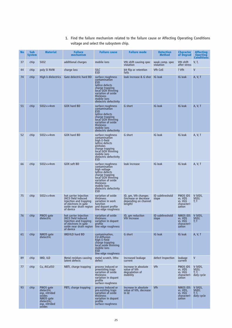
25
no Sub System
Material Failure mechanism
Failure cause Failure mode Detection Method
Character of Degrad
Affecting operting
Conditions
37 chip SiO2 additional charges mobile ions Vth shift causing spec violation
weak comp. spec violation
Vth shift after stress
V, T,
44 chip poly Si NVM charge loss SILC ESD
bit flip or retention fails
Vfh Cell ? Vfh V
74 chip High k dielectrics Gate delectric hard BD surface roughness contamination ESD lattice defects charge trapping local GOX thinning variation of oxide thickness mobile ions dielectric defectivity
leak increase & G shor IG leak IG leak A, V, T
51 chip SiO2<=4nm GOX hard BD surface roughness contamination ESD lattice defects charge trapping local GOX thinning variation of oxide thickness mobile ions dielectric defectivity
G short IG leak IG leak A, V, T
52 chip SiO2<=4nm GOX hard BD surface roughness contamination high E-field lattice defects pinholes charge trapping local GOX thinning mobile ions dielectric defectivity ESD
G short IG leak IG leak A, V, T
66 chip SiO2<=4nm GOX soft BD surface roughness contamination high voltage lattice defects charge trapping local GOX thinning variation of oxide thickness mobile ions dielectric defectivity ESD
leak increase IG leak IG leak A, V, T
75 chip SiO2<=4nm hot carrier injection (HCI) field induced injection and trapping of electrons in gate oxide near drain region of device
variation of oxide thickness variation in work function and dopant profile line edge roughness
ID, gm, Vth changes (increase or decrease depending on channel length)
ID subthreshold slope
PMOS IDS vs. VDS vs. VGS characteri-zation
V (VDS, VGS); T; f
76 chip PMOS gate dielectric
hot carrier injection (HCI) field induced injection and trapping of electrons in gate oxide near drain region of device
variation of oxide thickness variation in dopant profile line edge roughness
ID, gm reduction Vth increase
ID subthreshold slope
NMOS IDS vs. VDS vs. VGS characteri-zation
V (VDS, VGS); T; f
61 chip NMOS gate dielectric
IMD/ILD hard BD contamination, CU-diffusion high E-field charge trapping local oxide thinning mobile ions ESD line edge roughness
G short IG leak IG leak A, V, T
89 chip IMD, ILD Metal residues causing latent defects
metal scratch, litho defect
increased leakage current
defect inspection leakage current
V
77 chip Cu, AiCu(Si) NBTI, charge trapping process induced or preexisting traps variation of oxide thickness variation in dopant profile surface roughness
increase in absolute value of Vth degradation of mobility
Vfh PMOS IDS vs. VDS vs. VGS characteri-zation
V (VDS, VGS); T; f; duty cycle
93 chip PMOS gate dielectric esp. nitrided oxidesNMOS gate dielectric; esp. nitrided oxides
PBTI, charge trapping process induced or pre-existing traps variation of oxide thickness variation in dopant profile surface roughness
Increase in absolute value of Vth, decrease in ld
Vfh NMOS IDS vs. VDS, vs. VGS characteri-zation
V (VGS, VGD); T; f, duty cycle
1. Find the failure mechanism related to the failure cause or Affecting Operating Conditions voltage and select the subsystem chip.
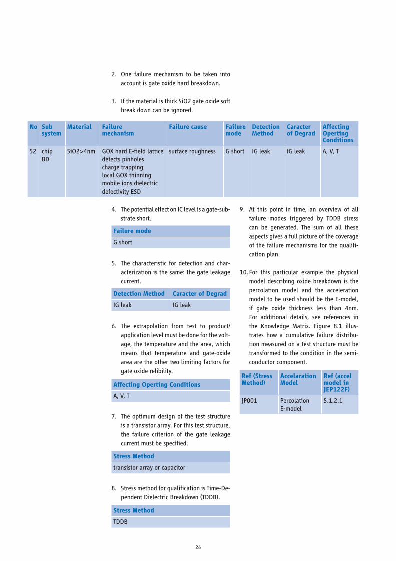
26
2. One failure mechanism to be taken into account is gate oxide hard breakdown.
3. If the material is thick SiO2 gate oxide soft break down can be ignored.
4. The potential effect on IC level is a gate-sub-strate short.
5. The characteristic for detection and char-acterization is the same: the gate leakage current.
6. The extrapolation from test to product/ application level must be done for the volt-age, the temperature and the area, which means that temperature and gate-oxide area are the other two limiting factors for gate oxide relibility.
7. The optimum design of the test structure is a transistor array. For this test structure, the failure criterion of the gate leakage current must be specified.
8. Stress method for qualification is Time-De-pendent Dielectric Breakdown (TDDB).
9. At this point in time, an overview of all failure modes triggered by TDDB stress can be generated. The sum of all these aspects gives a full picture of the coverage of the failure mechanisms for the qualifi-cation plan.
10. For this particular example the physical model describing oxide breakdown is the percolation model and the acceleration model to be used should be the E-model, if gate oxide thickness less than 4nm. For additional details, see references in the Knowledge Matrix. Figure 8.1 illus-trates how a cumulative failure distribu-tion measured on a test structure must be transformed to the condition in the semi-conductor component.
no Sub system
Material Failure mechanism
Failure cause Failure mode
Detection Method
Caracter of Degrad
Affecting operting Conditions
52 chip BD
SiO2>4nm GOX hard E-field lattice defects pinholes charge trapping local GOX thinning mobile ions dielectric defectivity ESD
surface roughness G short IG leak IG leak A, V, T
Failure mode
G short
Detection Method Caracter of Degrad
IG leak IG leak
Affecting operting Conditions
A, V, T
Stress Method
transistor array or capacitor
Stress Method
TDDB
Ref (Stress Method)
Accelaration Model
Ref (accel model in Jep122f)
JP001 Percolation E-model
5.1.2.1

27
8.3 limits of Accelerated Reliability Test-
ing
When creating a stress test plan certain physical and procedural limitations have to be taken into account.
8.3.1 limited load Capacity (Stressabil-ity) of Devices and Test Structures
Test structures are used because of their specific properties like:• Sensitivity to a single failure mechanism• Easy to analyze• Easy to characterize and measure• High load capacity (much higher than a
normal product)
They are used in qualification tests which are designed to generate degradation under accelerated stress conditions in a very short time. The load one can apply to test structures is physically limited by the maximum value before the failure mechanism changes. Typical examples for these limits are:• Local heating resulting in material
structure changes, diffusion path changes• Avalanche region of pn junctions for
standard voltage acceleration• Breakdown voltage of dielectrics if
degradation is evaluated• ESD failures if ESD is not the topic of
investigation• Current densities in EM tests of
interconnects which generate melting
8.3.2 library elements
Library elements are also used in stress tests. Their specific properties are:• Basic design elements• Easy to analyze• Easy to characterize and measure• No overstress capability
They are used in qualification tests, which are designed to generate parameter degradation under elevated operating conditions in a short time. Their stress capability is limited because:• No ESD protection• Current density and voltage stress limited
by design rules
8.3.3 Electronic Components (Products)
In some cases the electronic component is best suited for being used in a qualification tests due to the following properties• Performance according to spec• Robust under operating conditions• Protection circuitry
Limits for the application of electronic com-ponents are:• T
stress limited by mould compound or bonding
• Vstress
limited by protection circuitry• I
stress limited by voltage regulation
• Failure analysis limited by available resources• Stress coverage of el function hard to evaluate
F @Lifetime(F = cumulativefailure density)
Target Lifetime(e.g. 10 y)
VoltageExtrapolation
TemperatureExtrapolation
StatisticalExtrapolation
AreaExtrapolation
Measured IntrinsicDielectricFailure Distribution
log(time)
ln(-
ln(1
- F
))
t63% stress
t63% use
tlife
Figure 8.1 Extrapolation of Failure Distribution

28
8.3.4 limits of Application Range of Test Methods
Stress tests could be restricted to:• Certain technologies• Certain materials• Certain parameter ranges
Example Helium Fine Leak Test:• Designed to evaluate hermeticity of MEMS
packages• Perfect for metallic seals• For polymer sealed packages of no use due
to absorption properties of polymers
8.3.5 limited Resources for Reliability Evaluation
Resources for reliability evaluation are limited because high level experts and test equipment are needed. On the other hand the project schedule limits the available time for these activities. Time when information for produc-tion decision has to be available is defined by market, not related to the complexity of the problem.Therefore resources have to be concentrated on the most critical issues, preferably during the early phase of development. Activities which do not generate information have to be avoided. The trade-off between residual risk, costs and time-to-market has to be found for every product.
8.3.6 limited Time for Implementation of lessons learnt
The number of new materials and process recipes increases with every new technology generation.With every new material or process:• The criticality of failure mechanisms have
to be reviewed. New failure mechanisms are very rare, but what has been totally uncrit-ical in the past can be a major issue in the future.
• The degradation model parameters have to be evaluated and verified.
• The statistical model has to be evaluated and verified.
• Stress test conditions have to be developed.• Analysis technologies have to be developed.
The frequency of introducing new technolo-gies stays constant or might increase in the future.• The time for implementing the results of the
new reliability methodology has to be used more efficient to reach the targets.
• The resources have to be focused.
8.3.7 limited knowledge on Models and Failure Mechanisms
Keep in mind that the qualification statement is statistical in nature:• Extrapolation from stress to operating con-
ditions• The qualification statement describes the
situation at a certain point in time• Defects and maverick phenomena on low
failure level have to be covered by contain-ment activities
RV performed correctly generates the basic information to achieve ppm levels but qualifi-cation cannot demonstrate these levels statis-tically see also Section 9.5.A lot of progress has been made to understand the physics behind the failures, but a continu-ous effort is needed.

29
Each Qualification Plan consists of three basic elements:• Characterization plan (Section 9.5)• Reliability test plan (Section 9.2)• Demonstration of manufacturability (Sec-
tion 9.5.1)• A basic consideration how to select the
appropriate qualification strategy is des-cribed in section 9.1 using a flow created for AEC Q100/101
9.1 relation to Aec-q100/101 Stress
Test Conditions and Durations
In the early phase of a development project a decision has to be made on the appropriate qualification strategy and the standard to be applied.“Two flow charts are available to facilitate both Tier 1 and Semiconductor Component Supplier in a reliability capability assessment:• The flow chart in figure 9.3, describes the
process at Semiconductor Component Supplier to assess whether a new compo-nent can be qualified according to AEC-Q100/101.
• The flow chart in appendix E, describes (for details see Handbook for Robustness Val-idation of Automotive Electrical/Electronic Modules, ZVEI)
• (1) the process at Tier 1 to assess whether a certain electronic component fulfills the requirements of the mission profile of a new Electronic Control Unit (ECU), and
• (2) the process at Semiconductor Com-ponent Manufacturer to assess whether an existing component qualified accord-ing to AEC-Q100/101 can be used in a new application.
In summary, the flow charts result in the fol-lowing three clear possible conclusions:A] AEC-Q100/101 test conditions do apply.B] Mission Profile specific test conditions may
apply.
C] Robustness Validation may be applied with detailed alignment between Tier1 and Semiconductor Component Manufacturer.
In addition, not shown in the flow charts, the expected end of life failure probability may be an important criterion. Regarding failure probabilities, the following points should be considered:• No fails in 231 devices (77 devices from
3 lots) are applied as pass criteria for the major environmental stress tests in AEC Q100/101. This represents an LTPD (Lot Tolerance Percent Defective) = 1, meaning a maximum of 1 % failures at 90 % confi-dence level.
• This sample size is sufficient to identify intrinsic design, construction and/or mate-rial issues affecting performance.
• This sample size is NOT sufficient or intended for process control or PPM eval-uation. Manufacturing variation failures are kept under control by proper process controls and/or screens such as described in AEC-Q001, -Q002.
• Three lots are used as a minimal assurance of some process variation between lots. A monitoring process has to be installed to keep process variations under control.
• Sample sizes are limited by part and test facility costs, qualification test duration and limitations in batch size per test. A detailed description of flow chart steps is given below (numbers refer to these specific flow chart steps).”
9.1.1 basic Assessment
1.1 Items to consider in constructing a Mis-sion Profile Assessment:
• Type of application• Requirements of service life and usage• Environmental conditions / Mounting
location • Construction of the ECU• Power Dissipation of ECU and components• Reliability requirements in terms of lifetime
and related failure probabilities
9. creation of the qualification plan
Note:Direct references from AEC Q100 are in Italic. Similar statements can be found in AEC Q101.
30
A structured analysis of the mission profile will identify potential reliability risks in an early stage of development cycle, so that these risks can be addressed by appropriate component selection and validation.
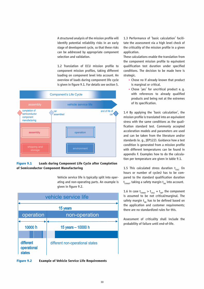
1.2 Translation of ECU mission profile to component mission profiles, taking different loading on component level into account. An overview of loads during component life cycle is given in figure 9.1. For details see section 5.
Vehicle service life is typically split into oper-ating and non-operating parts. An example is given in figure 9.2.
1.3 Performance of ‘basic calculation’ facili-tate the assessment via a high level check of the criticality of the mission profile in a given application.These calculations enable the translation from the component mission profile to equivalent qualification test duration under specified conditions. The decision to be made here is strategic.
• Chose no if already known that product is marginal or critical.
• Chose ‘yes’ for uncritical product e. g. with references to already qualified products and being not at the extremes of its specification.
1.4 By applying the ‘basic calculation’, the mission profile is translated into an equivalent stress with the same conditions as the quali-fication standard test. Commonly accepted acceleration models and parameters are used and can be taken from the literature and/or standards (e. g., JEP122). Guidance how a test condition is generated from a mission profile with different temperatures can be found in appendix F. Examples how to do the calcula-tion per temperature are given in table 9.1.
1.5 This calculated stress duration tCALC
(in hours or number of cycles) has to be com-pared to the standard qualification duration tSTAND
, taking a safety margin tSM
into account.
1.6 In case tSTAND
> tCALC
+ tSM
, the component is assumed to be not critical/marginal. The safety margin t
SM has to be defined based on
the application and customer requirements; there are no standardized rules for this.
Assessment of criticality shall include the probability of failure until end-of-life.
vehicle service life
15 yearsoperation non-operation
10000 h 15 years – 10000 h
differentoperationalstates
different non-operational states
Figure 9.1 loads during Component life Cycle after Completion of Semiconductor Component Manufacturing
operation
environment
assembly
shipping andstorage
Component’s Life Cycle
completion ofsemiconductorcomponentmanufacturing
end of life ofcar
carassembled
assembly vehicle service life
figure 9.2 example of Vehicle Service life requirements

31
The possibility to perform the qualification according to AEC Q100/Q101 or determine if additional testing and/or data is required, because the combination of this component in this application is critical or marginal, deter-mines the next step. The choice is:• Yes: It is critical or marginal, requiring
further analysis as to what new tests/condi-tions/data are required for qualification
• No: The standard AEC Q100/Q101 require-ments are appropriate for this application/component combination
A: Conclusion: perform qualification accord-ing to AEC Q100/Q101 test conditions
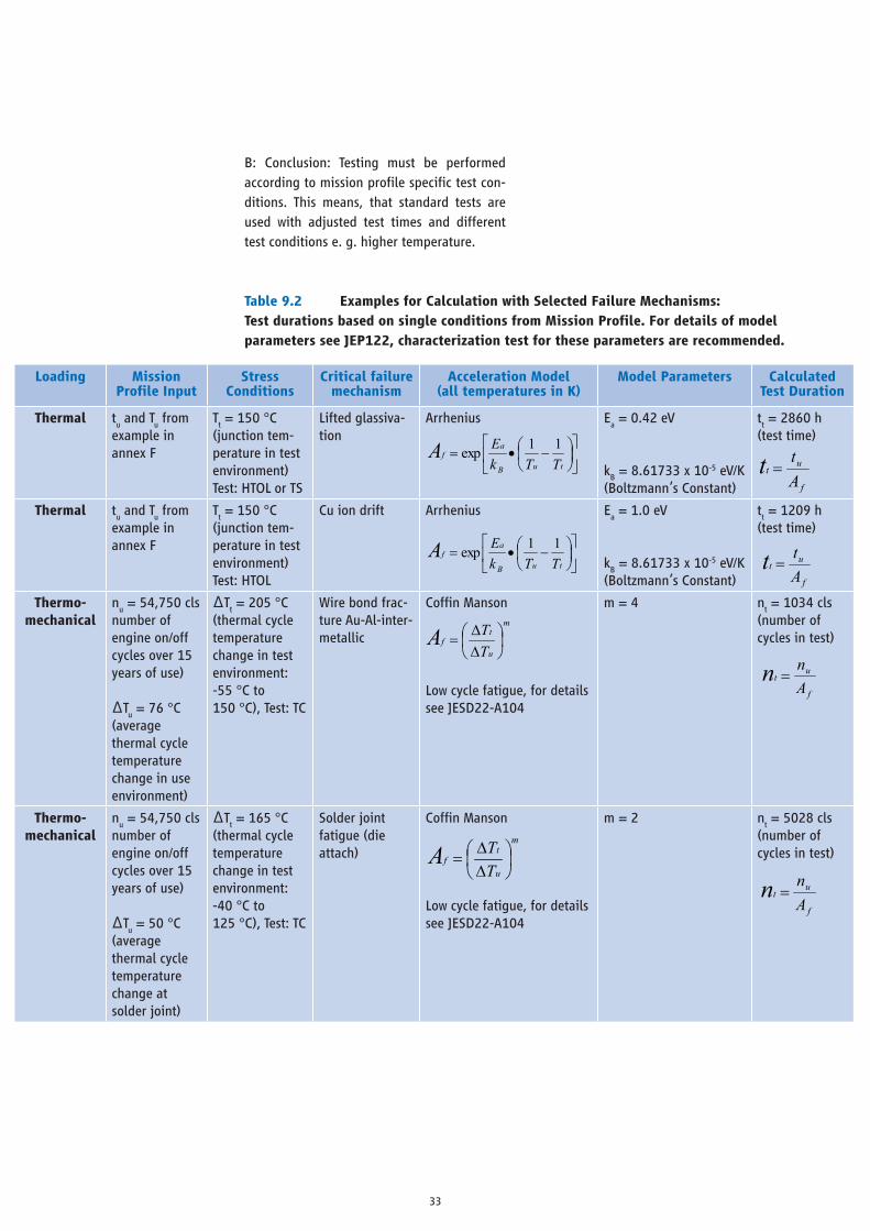
Table 9.1 Examples for basic Calculation: test durations based on single conditions from Mission profile
loading Missionprofile Input
StressConditions
Acceleration Model(all temperatures in K)
Model Parameters Calculated Test Duration
Thermal
tu (use time)
and Tu (use
temperature) from example in annex F
Tt = 150 °C
(junction tem-perature in test environment)
Arrhenius Ea = 0.7 eV
(activation energy; 0.7 eV is a presumed value, actual values depend on failure mechanism and range from -0.2 to 1.4 eV)
kB = 8.61733 x 10⁻⁵ eV/K
(Boltzmann’s Constant)
tt = 1695 h
(test time)
Thermo-mechanical
nu = 54,750 cls
number of engine on/off cycles over 15 years of use)
∆Tu = 76 °C
(average thermal cycle temperature change in use environment)
∆Tt = 205 °C
(thermal cycle temperature change in test environment:-55 °C to 150 °C)
Coffin Manson m = 4(Coffin Manson exponent; 4is a presumed value and to be used for cracks in hard metal alloys, actual values depend on failure mechanisms and range from 1 for ductile to 9 for brittle materials)
nt = 1034 cls
(number of cycles in test)
Humidity&
Temperature
tu = 3,000 h
(engine off time over 15 years of use)
RHu = 91 %
(average relative humidity in use environment)
Tu = 27 °C
(average tem-perature in use environment)
RHt = 85 %
(relative humidity in test environ-ment)
Tt = 85 °C
(ambient tem-perature in test environment)
Hallberg-Peck p = 3(Peck exponent, 3 isa pre-sumed value and to be used for bond pad corrosion)
Ea = 0.8 eV
(activation energy; 0.8 eV is a presumed value)
kB = 8.61733 x 10⁻⁵ eV/K
(Boltzmann’s Constant)
tt = 24.5 h
f
ut
Att =
−•=
tuB
af
TTkEA 11exp
m
u
tf
TTA
∆∆
=
f
ut
Ann =
−••=
tuB
a
u
t
p
fTTk
ERHRHA 11exp f
ut
Att =
0 20 40 60 80 100 120 140 160 180
7000
6000
5000
4000
3000
2000
1000
Operation time* [h]
Tj [°C]-40 -20

32
9.1.2 Mission profile Validation on Component level
2.1 The recommended base for assessing the critical failure mechanism(s) is the Robustness Validation Knowledge Matrix or JEP122. Risk assessment should be performed covering at least the following main considerations:• New materials or interfaces• New design or production techniques• Critical use conditions
Methods for risk assessment could be FMEA (AIAG Manual), Risk Assessment, FTA or sim-ilar.
2.2 In case acceleration models are in use in the company or known from the literature, they can be taken to perform lifetime calcu-lations. Experiments, simulation, or literature study can be used to create such acceleration models. Sufficient acceleration may be impos-sible due to limiting physical boundary con-ditions. In such a case minimum stress times should be defined to demonstrate sufficient robustness margin, (e. g., based on change or degradation of any electrical or physical prop-erties during or after stress and the impact on the specific application).
2.3 The acceleration model is used to calcu-late the acceleration factor for the standard stress condition. This in return gives the cal-culated minimum required stress time t
CALC (in
h or number of cycles) to demonstrate reliabil-ity without failures. Two examples for thermal and thermo-mechanical loading are described in table 9.2. It is assumed that the failure mechanisms listed in column 4 are critical for the intended application with the mission profile described in column 2. Column 3 gives a proposed stress test and condition. The cal-culated test duration in the last column refers to this stress condition. The standard test con-dition has to be adapted to these test times. An example for an additional test, which is not covered by standards like AEC Q100, is listed in table 9.3. It should be done in addition to standard testing.
2.4 A comparison with the standard qualifica-tion duration t
STAND is to be made. In case t
STAND
> tCALC
+ tSM
, the component is assumed to be not critical/ marginal. The robustness margin t
SM has to be defined based on the application
and customer requirements. Assessment of criticality shall include the accumulated fail-ure probability until end-of-life. Criteria for a decision shall include not only test conditions and durations as compared to the standard, but also coverage of critical failure mecha-nisms by the tests. Such coverage consider-ations include applicability of assumptions used in calculating the stress conditions, such as variation of the activation energy for differ-ent failure mechanisms. Beyond that it has to be assessed, if particular failure mechanisms are addressed by the standard test method at all. A case in point is active cycling of power devices, which is not adequately addressed by standard qualification tests. In addition, spe-cific requirements regarding fail probabilities may not be covered by standard test proce-dures. MIM capacitors, for instance, are known to fail due to extrinsic defects. A requirement of, e. g., less than 100 ppm for extrinsic fail-ures is not covered by standard tests and sam-ple sizes. The assessment should be aligned with Tier1.
2.5 In case the component standard qualifica-tion is not sufficient the supplier may define additional tests on product level or change the test conditions to close the gap between Q100/101 coverage and mission profile requirement.
2.6 The possibility to create additional data (Flow Chart 1) or show that additional data is not critical/ marginal determines the next step. The choice is• Yes: It is possible to find additional tests on
product level or to change the test condi-tions to close the gap between Q100/101 coverage and mission profile requirement.
• No: It is not possible to demonstrate the fulfillment of the reliability requirements according to mission profile by a test on product level.
33
B: Conclusion: Testing must be performed according to mission profile specific test con-ditions. This means, that standard tests are used with adjusted test times and different test conditions e. g. higher temperature.
table 9.2 Examples for Calculation with Selected Failure Mechanisms:test durations based on single conditions from Mission profile. for details of model parameters see Jep122, characterization test for these parameters are recommended.
loading Missionprofile Input
StressConditions
Critical failure mechanism
Acceleration Model(all temperatures in K)
Model Parameters Calculated Test Duration
Thermal tu and T
u from
example in annex F
Tt = 150 °C
(junction tem-perature in test environment)Test: HTOL or TS
Lifted glassiva-tion
Arrhenius Ea = 0.42 eV
kB = 8.61733 x 10⁻⁵ eV/K
(Boltzmann’s Constant)
tt = 2860 h
(test time)
Thermal tu and T
u from
example in annex F
Tt = 150 °C
(junction tem-perature in test environment)Test: HTOL
Cu ion drift Arrhenius Ea = 1.0 eV
kB = 8.61733 x 10⁻⁵ eV/K
(Boltzmann’s Constant)
tt = 1209 h
(test time)
Thermo-mechanical
nu = 54,750 cls
number of engine on/off cycles over 15 years of use)
∆Tu = 76 °C
(average thermal cycle temperature change in use environment)
∆Tt = 205 °C
(thermal cycle temperature change in test environment: -55 °C to 150 °C), Test: TC
Wire bond frac-ture Au-Al-inter-metallic
Coffin Manson
Low cycle fatigue, for details see JESD22-A104
m = 4 nt = 1034 cls
(number of cycles in test)
Thermo-mechanical
nu = 54,750 cls
number of engine on/off cycles over 15 years of use)
∆Tu = 50 °C
(average thermal cycle temperature change at solder joint)
∆Tt = 165 °C
(thermal cycle temperature change in test environment: -40 °C to 125 °C), Test: TC
Solder joint fatigue (die attach)
Coffin Manson
Low cycle fatigue, for details see JESD22-A104
m = 2 nt = 5028 cls
(number of cycles in test)
−•=
tuB
af
TTkEA 11exp
f
ut
Att =
−•=
tuB
af
TTkEA 11exp
f
ut
Att =
m
u
tf
TTA
∆∆
=
f
ut
Ann =
m
u
tf
TTA
∆∆
=
f
ut
Ann =

34
9.1.3 Robustness Validation on Compo-nent level
C: Conclusion: Testing must be performed according to mission profile requirements following the Robustness Validation strategy with focus on critical failure mechanisms and measuring failure distributions. The test plan shall be aligned between CM and Tier 1.
Process for qualification plan generation based on mission profile:a. List all conditions, operating, non-operat-
ing, production or transport with all rel-evant parameters like temperature, tem-perature cycles, humidity or other and the correspondent time the condition applies.
b. For a temperature mission profile all peri-ods with identical temperatures are sum-marized. An example for one condition of a temperature mission profile is given in line 1 of table 9.1. For a predefined stress condition each of the conditions can be quantified using the acceleration model, here the Arrhenius model. The result is the equivalent stress time.
c) For a temperature cycling and a humidi-ty-temperature example the calculation is shown in line 2 and 3 using the Cof-fin-Manson and Hallberg-Peck model.
Table 9.3 example for an Additional test required by Specific Application
loading Missionprofile Input
StressConditions
Critical failure mechanism
Acceleration Model(all temperatures in K)
Model Parameters Calculated Test Duration
Thermo-mechanical
nu = 11,000 cls
number of cold starts over 15 years of use)
∆Tu = 80 °C
(average thermal cycle temperature change in use environment)
∆Tt =165 °C
(thermal cycle temperature change in test environment: -40 °C to 125 °C), Test: TC
2nd level (board level) solder joint fatigue
Norris-Landzberg
Modification according to Pan N. et al, Proc. SMTA, 2005
a = 2.65b = 0.136c = 2185
nt = 865 cycles
(number of cycles in test)
−
∆∆
=su
b
u
ta
u
t
TTc
tt
TT
fAmax,max,
11exp
f
ut
Ann =

35
9.1.4 Application note
It should be taken into account, that a Qualifi-cation plan could consist out of tests from all three approaches A-C depending on the fail-ure mechanisms to be covered and the techni-cal capabilities.
Determine mission profileof the componentincluding loading
Determine critical FailureMechanisms
Calculate test durationwith standard accelerationmodels for standard tests
and test conditions
Calculate test durationwith selected accelerationmodels for standard tests
and test conditions
Perform Qualificationaccording to AEC-Q100
Test conditions
Yes
No
Yes
Mission Profile Validation on Component Level
No
Basic Assessment
Basiccalculation?
More severethen AEC-
Q100?
No Yes
1.1
1.2
1.3
1.4
1.5
1.6
2.1
2.2
2.3
2.4
Determine Mission Profileon ECU level
Compare with AEC-Q100test conditions
Yes
Determination of reliability test criteria for a new component basedon mission profile requirements of intended application
Process at Component Manufacturer (CM):Assess whether a new component can be qualified according to AEC-Q100 test conditions
Critical/Marginal?
Determine accelerationmodels
Define additional testsand/or test conditions Possible?
Perform testingaccording to MissionProfile specific test
conditions
No
A 2.5
2.6
Responsibility
Tier 1 CM Tier 1 +CM
Perform RobustnessValidation with
detailed alignmentbetween SCM andTier 1 on mission
profile and/or criticalfailure mechanisms*
Robustness Validationon Component Level
B
C
* Note that this flow chart does not coverthe consideration of AEC acceptancecriteria based on LTPD-sampling plan(max. of 1% failures allowed) versus theRobustness Validation failure rateextrapolation
Figure 9.3 Flow Chart 1 – Reliability Test Criteria for new Component

36
9.2 reliability test plan
All failure mechanisms that have been iden-tified as potential risks must be addressed by reliability data. Information already existing from previous investigations or data from the development work could be used to confirm low risk levels (see also Section 6). The appli-cability of generic data must be demonstrated.Some types of input to the Qualification Plan could be extracted from the knowledge database:• The test structure that could be used for
reliability characterization. Circuits, sub circuits, library elements, or the complete semiconductor component should be con-sidered as the appropriate test structure. Criteria such as availability or analysability should also be taken into account.
• The stress method that could be used to address and accelerate the failure mechanism.
Special attention must be given to the failure rate of the specific test structure. There is no generic rule about the manner in which this number is calculated from the failure rate tar-get of the product because of the potential dif-ference in the failure paretos. If, for example, one failure mechanism dominates the failure rate of the product, the assumption that more than 50 % of the product failure rate may be due to this dominant mechanism is reasona-ble. However, if several failure mechanisms have comparable failure rates, the product failure rate must be distributed among them.For the assessment of reliability, the Qualifi-cation Plan shall contain the following infor-mation for every stress test:• Targeted failure mechanism(s), including an
explanation of relevance (give rationale if the typical failure mechanisms are rated as irrelevant).
• Acceleration model used.• Vehicle (= test structure): The test structure
must be representative of or related to the product design and the application condi-tions that the product may experience in the field. This may require detailed documen-tation.
• Stress method.• Stress conditions (parameterization of the
stress test): Stress conditions must be opti-mized with respect to the failure mechanism to be addressed.
• Sample size or number of lots: Qualification shall provide statistically valid data for the demonstration of intrinsic failure mecha-nisms. Failure rates in the range of ppm at the product level cannot be demonstrated in the qualification phase.
• Parameter for characterization (P) of the test structure.
• Method of failure analysis for characteriza-tion, if needed.
• Fail criteria (Pfail
) or acceptance criteria• Readout times or intervals and criteria for
the end of test.
In certain instances, reliability validation may also require verification at the ECU level. This can only be accomplished by the user of the component and requires agreement and coop-eration between the manufacturer of the com-ponent and the user.
An example and template that includes these elements in a qualification plan is shown in Appendix A. For every reliability characteri-zation, a target value is needed as a gate to separate the failure case from the expected performance according to its requirement. This target value is applied to the parameter P that is used for characterization of the deg-radation during stress. In some cases, P
target is
not directly defined as a requirement. In such cases, the relationship between the require-ment and P must be known. The target value could be a lower or upper limit or a range and shall include the relevant tolerances.
37
The characterization column of the Knowledge Matrix indicates which parameter should be measured during stress to generate the deg-radation over time. To calculate the lifetime under stress conditions, a fail criterion must be defined that is related to the requirements or the spec values. Examples for degradation parameters are:• Leakage current for gate oxide related failure
mechanisms.• Resistance for electro- and stress migration.• Transistor parameters (such as threshold
voltage, drain current or transconductance).
Acceleration may be limited due to items such as competing failure mechanisms or the intrinsic robustness of the system or design. An insufficient number of failures may occur during economically acceptable test duration (for example, due to physical boundary condi-tions). There is no generic solution that fits all cases, but potential options are:• Choose more sensitive failure criteria and
correlate the results.• Increase the sample size and stop the test
after the first part of the failure distribution has been measured.
• When only a portion of the distribution fails, the statistical solution for lognormal distributions is described in JESD 37; for other cases, see e. g. [15].
• If there is no failure, one could make the following assumptions and estimate the lifetime of the failure mechanism:
- Use a known model and typical parameters (such as for lognormal distribution).
- Assume that the first device under test fails right at the end of stress time.
Before performing many expensive and time-consuming qualification tests, it should be determined whether data are already avail-able that demonstrate the robustness of the semiconductor component with respect to a certain failure mechanism. These generic data could have been generated by testing an object different from the one under discussion, but the data may be valid for a group of objects. An object could be a semiconductor component, a package, a wafer – or a package technology.
These groups of objects – called qualification families – could consist of wafer technologies or parts of it, assembly technologies or parts of it, packages, or semiconductor components with similar functions, specifications or appli-cation conditions. The relevance of the appli-cation of generic data must be supported by other documents or data.
A qualification family will be defined by its manufacturing attributes (material, site and processes).Examples:• A die family will be defined by its wafer fab
attributes.• A package family will be defined by its
assembly attributes only.
Family definitions, test results and the appli-cability of those must be clearly communi-cated to the customer.
Example for one failure mechanism – electromigration:A certain functionality required by the cus-tomer of an electronic component can be achieved only if the product has a certain complexity. The minimum feature size of the technology could be defined from the required complexity. This minimum feature size is associated with a maximum current density in interconnects, which together with a corresponding lifetime and failure rate, is a reliability target for the reliability qualifi-cation of the technology. The failure mecha-nism related to current density is electromi-gration. The failure criterion is defined by the maximum resistance change tolerated by the design of the product. In this case, the critical parameter for reliability qualification is ΔP = ΔR. By applying reduced current densities to a design, the target failure rate could be reduced or the lifetime could be prolonged by keeping the failure rate constant.

38
9.3 definition of a qualification family9.3.1 Wafer Fab
All semiconductor components using the same technology, process and materials with com-mon major elements (such as 90 nm effective channel length, Cu metallization, intermetal dielectric material, shallow trench isolation), are categorized as one qualification fam-ily and are qualified by association when one family member is successfully qualified. Family re-qualification is required when the process or material is changed significantly (major process changes). Typical considera-tions for wafer fab process descriptions are: design rules, lithography technique, metalli-zation, polysilicon, dielectrics etc.
9.3.2 Assembly processes
The processes for plastic and hermetic pack-age technologies must be considered and qualified separately. All semiconductor com-ponents using the same process and mate-rials, with common major elements (such as biphenyl mold compound, Alloy 42 lead-frame material, Pb-free lead plating), are categorized as one qualification family and are qualified by association when one fam-ily member is successfully qualified. Family re-qualification is required when the process or material is changed significantly (major process changes). Typical considerations for assembly process description: leadframe, die attach, package material, bonding, external lead finish etc.
9.4 qualification envelope
For ASICs, the alignment of requirement with the specification of technology and semicon-ductor component can be done by direct cor-relation. For cases in which a broad spectrum of applications must be addressed, an adapted approach for generating the qualification plan must be applied. Taking the worst-case values for each specified characteristic separately is one way to create this envelope (specification X in Figure 9.4). In many cases, however, this procedure leads to overly conservative spec-ification, unnecessarily increasing the cost of development and qualifications. It is advanta-geous to define the envelope in more detail to generate an efficient solution (specification R). Figure 9.4 illustrates the difference between the two approaches for two spec parameters A and B.
The more efficient approach fulfils the same requirement from Applications 1 and 2 and prevents over-engineering.
In cases where specific applications are not known, it becomes a strategic decision as to how to define the spec area of the semicon-ductor component and the correspondent qualification envelope. The trade-off between costs, Robustness Margin, and spec area must be found based on generic market informa-tion. In this case, the robustness of the semi-conductor component must be measured with respect to this generic specification, so that the robustness for an in tended application
Figure 9.4 Specification options for different Applications
Para
met
er B
Parameter A
Specification R
Specification X
Appl. 1
Appl. 2

39
Note:The user shall not exceed agreed upon speci-fication limits under any circumstances. Char-acterization beyond specification limits is for information on robustness only. If at any time a part is found to operate, during the applica-tion, beyond the agreed upon limits, requires agreement by both parties, especially legal and financial indemnification to the supplier on the part of the user.
can be calculated in the process of choosing a semiconductor component for a specific mod-ule design. This means, for instance, that the same product could fit into a safety relevant application with lower spec values and high robustness and fit into an uncritical appli-cation with a higher spec value and lower Robustness Margin.
9.5 characterization plan
The Characterization Plan should include the plan for material and testing to ensure the functionality of the product over all produc-tion variations and all temperatures and volt-age ranges. Testing should be at both spec lim-its and beyond (as appropriate) to determine the margins. The plan should include process variability (that is, corner lot details) to show the range of production material. Data should be statistically summarized to show C
pk of each
parameter.
Any data from previous characterizations is also useful. The purpose of this is to make sure that the design and production are capable of maintaining specified C
pk values for all speci-
fied parameters.
9.5.1 process characterization
Process variability characterization may take the form of process corner matrix lots contain-ing groups of wafers that have one or more process steps varied by plus or minus several sigmas. If process variations cannot be pro-duced in a dedicated manner, test samples may be selected by using SPC data to identify wafers or test samples near or beyond the lim-its. The chosen process steps should be known to directly correlate to specific functions or
electrical parameters affecting the perfor-mance of the device in a given application. The packaged devices from this material can then be assembled into an automotive system to understand which region of the process space yields the best performing devices. This type of characterization should be performed for new supplier semiconductor component designs that have little or no relation to pre-vious designs, the first automotive applica-tion of an existing semiconductor component design, or a more demanding automotive application for an existing design. The char-acterization requirements may be reduced if appropriate data exists from other project(s).
1. Determine relevant failure modes of the semiconductor component that can affect the application.
2. Correlate these failure modes with the cor-responding process parameters that affect them.
3. Determine if there is independence between the failure modes and the corresponding process parameter. If not, a design-of-ex-periments may need to be performed.
4. Assign statistically significant sample sizes to each process corner split when perform-ing electrical testing.
5. Record variable electrical parameter data over extremes of temperature, voltage, fre-quency, and/or loading. The variables data for each parametric test should include a summary of mean, standard deviation, minimum, maximum, C
pk and upper and
lower spec limits for each process corner and extreme sampling.
These variability considerations should be done by appropriate simulations of critical sub circuits. Typical characterization plans may include the demonstration of process variability. This may be in the form of a corner lot plan including device parameters (thresh-old voltage V
t, effective channel length Leff,
etc.) to be varied and the expected effect on semiconductor component performance. The yield values shall be assessed with respect to the target yield and potential yield detractors should be used as a starting point for continu-ous improvement planning.

40
9.5.2 device (Semiconductor compo-nent) characterization
The characterization conditions depend on the component under consideration. For digi-tal circuits, typical characterization plans may include:• Min/Max operating parameters – tests that
find min/max conditions for supply voltage, bus timing, frequency, etc.
• Margin testing – voltage will be charac-terized to find the potential fail levels (I/O levels).
• Current level characterization – measure all leakage currents (I
dd etc.) to determine mar-
gins to the specification. - Power supply current level charac-
terization – measure Iddq
and ΔIddq
, to determine static test pattern and power supply current margins to the spec.
- Leakage current level characteriza-tion – measure all leakage currents. Measuring leakage as a condition of connecting V
cc/GND directly to CMOS
gate and determining the spec limit, in order to detect potential defects, helps to improve robustness.
• PLL characterization (stabilization time, lock, jitter).
• Oscillator parametric tests.
9.5.3 Production Part lot Variation characterization
Production parts from a centered process can be characterized over temperature, voltage, frequency and loading to understand its inher-ent variance. Devices from specific parametric extremes can then be assembled into a sys-tem to observe if the process centering yields weak regions in the process space. This type of characterization can also be used if process corner matrix lot characterization proves to be too expensive or time consuming for the anticipated benefit in yield and performance.
1. Decide on a statistically significant sample size if the entire lot is not to be tested.
2. Record variable electrical parameter data over extremes of temperature, volt-age, frequency, and/or loading for each
part tested. The variables data for each parametric test may include a summary of mean, standard deviation, minimum, maximum, C
pk and upper and lower spec
limits for each extreme sampling.3. If attribute data is to be taken, electrical
tests over extremes of temperature, volt-age, frequency and/or loading may result in Schmoo plots diagramming the func-tional parameter space within which the part will operate.
9.6 Sample Size and basic Statistics
Typically sample sizes available for qualifica-tion are small compared to the failure target which should be achieved under high vol-ume production of the electronic component. A Zero-Fail at stress strategy is only able to demonstrate that catastrophic problems are not expected to happen. This can easily be seen in Table 9.4 where the number of test devices are listed which are needed to demon-strate a certain failure number with 90 % confidence assuming that after the test no failure is detected. To give an example: 0/77 failures at 90 % CL demonstrates 30,000 dpm failures.
A failure distribution as shown in Figure 9.5 with 50 failed devices out of 77 samples could be used for extrapolating down to the ppm target level at a specific stress test time.
Table 9.4 required Sample Size for Different Failure Targets Assuming 90 % cl
samples failure (dmp)
4 100,000
231 10,000
462 5,000
2304 1,000
4606 500
23027 100
115130 20
232600 10

41
Figure 9.5 example of a Weibull probability plot for 50/77 failed devices Including 90 % confidence curve
Besides the knowledge on the failure mech-anism the RV concept generates statistical data, for a Weibull distribution the shape and the scale parameter (t63), to perform more powerful statistical analysis compared to the zero fail approach. Calculation of the 90 % CL curve of the extrapolation is also possible.
Note:The RV Method generates statistics knowledge which could be used for better risk analysis.
With known acceleration factor the extrapola-tion from stress to operating condition could be done.
Time (a.u.)
CDF F
(t) /
%
0.1 1000.01.0 10.0 100.01.00E-4
5.00E-4
1.00E-3
5.00E-3
0.01
0.05
0.10
0.50
1.00
5.00
10.00
50.00
90.00
99.00
1.00E-4
end of test

42
The stress tests must be performed according to the requirements specified in the Qualifi-cation Plan. The equipment must satisfy the requirements with respect to the stress test parameters as defined in the Qualification Plan, and the tolerances of the parameters must be known. The reference column of the Knowledge Matrix contains a detailed descrip-tion of the method and how to perform the test.Characterization data must be completely logged for all readouts. The test at readout must comprise the full program. There must not be a stop-on-first-fail nor must parameter values be substituted by error log values. The latter should only help to identify problems during testing. The parameter values will be needed for further drift/fail analysis. Critical parameters may be monitored continuously during the entire characterization procedure in order to react quickly and in a focused way in case of failures. The measurement fre-quency must be adapted to the level of accel-eration.
The output of the qualification test shall be documented with the parameters listed:• P = P(t), the change of the parameter over
the time of stress if there is a continuous degradation or
• Pi = P(ti), if there are discrete readout inter-
vals, denoted by the subscript i.• Fail distribution (TTF) under stress condi-
tion.• Confirmation is needed that the intended
failure mechanism has really been acti-vated. Different failures that may occur but are not correlated to the addressed failure mechanism must receive special attention and must be treated separately in the life-time/risk assessment. Such failure mecha-nisms may show up as irregularities in the degradation curve or failure distribution, such as bimodality.
• Model used to convert results from stress test to lifetime at use conditions.
• Other factors that must be taken into account, such as duty cycle.
Based on this information, the lifetime per failure mechanism can be calculated:• Lifetime under stress conditions t
stress
• Lifetime under use conditions tuse
In case of an unexpected behavior, updating the knowledge base must be taken into con-sideration. In cases where only a comparison is needed, a qualitative evaluation could be used. This procedure requires knowledge from previous RV.
10. Stress and characterization
Note:It is not useful to log parameters not related to the applied stress for all readouts.
Note:In some cases, only the time to (catastrophic) fail is recorded (example: in many cases, TC leads to catastrophic failures; for example, electrical failure due to cracking, that can-not be observed during degradation, that is the crack initiation and propagation). In such cases, only the time to fail, t
f, is available.
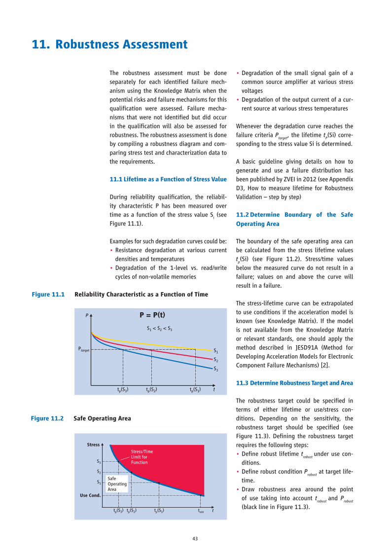
43
11. Robustness Assessment
t
P P = P(t)
Ptarget S1
S1 < S2 < S3
S2
S3
tp(S3) tp(S2) tp(S1)
t
Stress
Use Cond.
SafeOperatingArea
Stress/TimeLimit forFunction
S1
S2
S3
tp(S3) tp(S2) tp(S1) tuse
Figure 11.1 Reliability Characteristic as a Function of Time
figure 11.2 Safe operating Area
The robustness assessment must be done separately for each identified failure mech-anism using the Knowledge Matrix when the potential risks and failure mechanisms for this qualification were assessed. Failure mecha-nisms that were not identified but did occur in the qualification will also be assessed for robustness. The robustness assessment is done by compiling a robustness diagram and com-paring stress test and characterization data to the requirements.
11.1 lifetime as a Function of Stress Value
During reliability qualification, the reliabil-ity characteristic P has been measured over time as a function of the stress value S
i (see
Figure 11.1).
Examples for such degradation curves could be:• Resistance degradation at various current
densities and temperatures• Degradation of the 1-level vs. read/write
cycles of non-volatile memories
• Degradation of the small signal gain of a common source amplifier at various stress voltages
• Degradation of the output current of a cur-rent source at various stress temperatures
Whenever the degradation curve reaches the failure criteria P
target, the lifetime t
P(Si) corre-
sponding to the stress value Si is determined.
A basic guideline giving details on how to generate and use a failure distribution has been published by ZVEI in 2012 (see Appendix D3, How to measure lifetime for Robustness Validation – step by step)
11.2 determine boundary of the Safe
operating Area
The boundary of the safe operating area can be calculated from the stress lifetime values tp(Si) (see Figure 11.2). Stress/time values
below the measured curve do not result in a failure; values on and above the curve will result in a failure.
The stress-lifetime curve can be extrapolated to use conditions if the acceleration model is known (see Knowledge Matrix). If the model is not available from the Knowledge Matrix or relevant standards, one should apply the method described in JESD91A (Method for Developing Acceleration Models for Electronic Component Failure Mechanisms) [2].
11.3 Determine Robustness Target and Area
The robustness target could be specified in terms of either lifetime or use/stress con-ditions. Depending on the sensitivity, the robustness target should be specified (see Figure 11.3). Defining the robustness target requires the following steps:• Define robust lifetime t
robust under use con-
ditions.• Define robust condition P
robust at target life-
time.• Draw robustness area around the point
of use taking into account trobust
and Probust
(black line in Figure 11.3).

44
The robustness area around the point of use is bordered by the robustness limit (P, t). Within the robustness area, the product should be safe against the related failure mechanisms, which means that applying a value P over time t, with (P, t) lying inside the robustness area does not result in a failure. The limit also gives the designer the opportunity to choose the point of use according to different safety requirements.
An example for such a type of robustness tar-get could be the maximum allowed leakage current calculated based on the maximum allowed quiescent current over a use time of ten years of operation. The robustness target could be found by defining the robust value for the leakage current after 10 years of oper-ation and by defining the operation time with-out violation of the leakage current target. Values between this robustness targets could be found by interpolation.
11.4 Determine Robustness Margin
The robustness area is the reference for the robustness comparison (Figure 11.4). The measured data for P = P(t) (blue curve) shall be compared to the robustness target.
If the measured robustness curve (blue curve in Figure 11.4) is outside the target area (black boundary in Figure 11.4), the robustness per failure mechanism is sufficient. The blue bar defines the measured Robustness Margin with respect to a specific failure mechanism and a target value (see also Figure 4.2).
If the measured robustness is less than the target, measures for improvement of insuffi-cient robustness must be applied. These meas-ures are weighted by the severity of the effect of the failure.
Robustness Margin can be represented using the Robustness Indicator Figure (RIF). RIF is defined as the distance between the failure point (Pfailure or tfailure) and the requirements (P at use conditions or ttarget). Taking the time to measure Robustness Margin, then
RIF = tfailure
- ttarget
Because in general robustness of a parame-ter means that the parameter is lees sensi-tive to the change in the statistics of the input parameters (conditions of use, process varia-tions, etc.). Therefore, it is useful to introduce a deviation parameter σ to the RIF. Further-more, because reliability lifetimes are often Weibull or log-normal distributed, so ln(t) is used which is (approximately) normally dis-tributed. In analogy with C
pk, an RIF of a relia-
bility parameter is defined by
RIF = [ln(tfailure
) - ln(ttarget
)] / 3σ
• tfailure
= mean stress failure time of different sample sets at required failure rate
• ttarget
= required lifetime at stress conditions• σ = standard deviation of stress failure time
[ln(t)] of different sample sets and also may include deviation from use conditions.
Robustness Margin calculated with this RIF indicates not only the distance to the required target but also the sensitivity of response to the external variations.
Robustness RequiredRobustness Target BoundaryPoint of Use
t
P
Puse
Probust
ttarget trobust
t
Stress
Use Cond.
ttarget tuse
Robustness Measured (delta)Robustness Target
Figure 11.3 robustness target definition
Figure 11.4 Robustness Evaluation

45
12. Improvement
If the measured robustness is less than the target, there are several possible reactions. Some of the measures could be applied before the robustness measurement in the develop-ment phase. In all cases, this is the preferred approach. The following options for improve-ment are not sorted by priorities or effectiveness. Each option must be checked to determine which measure is the most effective and the most effi-cient and therefore has to receive top priority.
12.1 Stress Set-up review
When the evaluated robustness does not match the targeted level, the first step (least expensive) consists of a review of the set-up and the data.
The following points should be checked:• Confirmation of data:
- Are the stress conditions correctly defined (e. g. to avoid overstress that stimulates irrelevant failure mecha-nisms)? Is the equipment calibrated?
- Are the measurements conditions under control?
• Review of sample selection: - Are the samples representative for the
production? - Were weak engineering samples selected
for test? - Are the already stressed samples iden-
tified?• Feasibility of failure mode:
- Is there a good matching between tar-geted and obtained failure mode?
- What is the model used? - How are the model parameters used
from the extrapolation chosen?• Review of stress method:
- Is there a good matching between applied stress and targeted failure mechanism?
- Did the test comply with the appropri-ate industry standard test method (i. e., JEDEC, IEC)?
• etc.If the insufficient robustness is confirmed, improvement measures must be defined.
12.2 Mission profile review
A more detailed review of the Mission Pro-file, especially for the critical topics with low robustness values, should be performed to identify safety margins that have been added due to the lack of knowledge or data. The result of this activity could be a newly defined point of use. A tool like FMEA could support this activity to quantify the risks associated with critical topics.
12.3 Application review
The robustness of a product is reflected in the application. Improvements could be made by alignment of the system design with the user application through co-engineering activities between the supplier and the user. Designel-ated issues could be addressed if the supplier and the user are involved and understand the use application and requirements. Also, both design teams can become educated on proper device use and specification:• Check if a robustness target is required in detail.• More robust system design.• Part de-rating.
12.4 Screening Strategy
The screening strategy should be adapted to the failure rate target. It should address the failure mechanisms identified during the reliability qualification. The failure mecha-nism Knowledge Matrix could be used in the adapted stress method.The screening strategy should be based on:• Deployment of Part Average Testing to
detect and eliminate the outlier devices.• Deployment of Statistical Yield Analysis and
Statistical Bin Limit to separate the abnor-mal wafers.
• Standardization of tests programs: defini-tion of a basic test program template, based on frontend technology, blocks functional-ity, product and application specificities.
If burn-in is used to reduce failure rates, it must be demonstrated by a burn-in study that the relevant failure mechanism is really addressed. In some cases, the weak parts are related to certain locations on the edge of the wafer. If this is the case, the wafer edge exclusion zone can be changed to solve the problem [10].
46
12.5 design for reliability (dfr)
DfR is a powerful approach to prevent reliability problems in the application by early application of design measures. Therefore, the measures listed below should have been applied already during the design phase. Depending on the rea-sons for insufficient robustness, the enhancement of these measures should be discussed in this phase. Potential measures are:• Redundant design.• Combined with an adequate simulation tool
and the data of the RV, the weak links in the design could be identified and mitigated. Examples are redundant vias and broad-ened lines in the interconnect part of the semiconductor component.
• Reliability simulation.• Simulation should be performed again
using the RV results to improve the accuracy of the simulation data.
• Part de-rating.
12.6 technology/design Solution
Technology solutions are the set of smart solu-tions (coupling process, design, and application) able to resolve the RV gap. The comprehensive list cannot be provided here as these solutions require a case-by-case definition, but examples could be:• Junction temperature watchdog. This device
monitors the product operating junction temperature and is able to activate a low power mode with reduced functionality mode when the junction temperature is above a defined limit.
• Lowering voltage for voltage driven risks (pushing the process to its capability limit).
• Multiplying or removing critical elements, like decoupling capacitors, if they do not meet the Mission Profile requirements.
• Critical element redundancy and switch capability: The critical element (like a capacitor) is controlled via a defined cir-cuitry able to switch to a new capacitor if the first one fails.
• Use chip parasitic structures to clamp or bypass critical stress conditions.
• Use stress relief packages to absorb and limit damages related to mechanical con-straints if present in the application.
• Tighten process limit.• Chip redesign to address robustness issues.
If there is more than one option to improve the robustness, a trade-off must be found. The solu-tion depends on the weight of these factors:• Cost• Schedule• Quality• PerformanceWhen robustness improvement cannot be achieved by the means indicated above, the project situation and the related risks must be reviewed between the customer and the semi-conductor component supplier.The preferred strategy is to perform iterations in the definition of the product mission criti-cal elements in order to offer a more effective trade-off between risks, performance, devel-opment timing, development costs, semicon-ductor component cost, and end-user require-ments.A typical example of such a situation would be if the current prevention techniques do not enable the expected target in the Mission Pro-file to be met. A potential trade-off in such a situation is to increase the silicon size, and costs, to add error detection and correction circuitry, for instance at embedded DRAM spe-cific failure modes.Before implementing the solution for improv-ing robustness, the proposed solution must be reviewed with respect to several aspects:• Is the expected improvement good enough
with respect to the robustness target?• Does the solution influence the robustness
with respect to other failure mechanisms?• What is the implementation risk (probabil-
ity that the implementation fails)?In most cases, the solution of a problem of low robustness generates some basic knowledge.This could be:• New design strategies.• Better understanding of degradation or
extrapolation models.• Better understanding of Mission Profiles.This knowledge should be fed back to the cor-responding knowledge base to be made avail-able for the next generation of projects. New failure mechanisms or their model descrip-tion should be used to update the Knowledge Matrix (see Section 8.1).
Note:Continuous improvement to achieve the con-cept of ‘Zero Defects’ [6], while important and comprehensive in scope, is outside the pur-view of this document.

47
13. Monitoring
Note:A monitoring parameter may address more than one failure mechanism.
13.1 Planning
Qualification reflects the status of the product/ technology at a certain point in time, based on a certain limited sample size. The infor-mation and knowledge gathered during qual-ification serves to evaluate the parameters reviewed during RV with respect to their criti-cality during ramp-up and volume production. This evaluation is the basis of the definition of monitoring that is needed to control the sta-bility in the production phase. A template for the monitoring plan is included in the report-ing template.
Monitoring shall be based on a risk assess-ment that must identify potential failure mechanisms for the production phase includ-ing intrinsic and extrinsic failures, analo-gously to qualification. Identification may be based on, but is not restricted to:• Observation of failure mechanisms during
development and qualification.• Mechanisms covered in a FMEA.• Previous experience with products using
comparable materials and/or processes and production tools.
A monitor for each failure mechanism must be established. This monitor can address the parameters relevant to the failure mechanism at different levels. The monitoring parameters are typically chosen from different groups of parameters:• In-line process parameters using SPC.• Electrical parameters at the wafer level with
special focus on Key Parameters using SPC.• Final test parameters of the semiconduc-
tor component with special focus on Key Parameters using SPC.
• Defect related tests, like Iddq
or ΔIddq
.• Highly accelerated stress tests, such as fast
wafer level reliability (fWLR) tests.• Defect density monitors.• High voltage tests with the semiconductor
component.
• Specific tests on fl ash cells, such as erratic bit, moving bit, cycling endurance.
• PAT, SBA• Burn-in• Reliability monitoring using the semicon-
ductor component.
Monitoring of intrinsic failure mechanisms usually needs only small sample sizes, as in qualification. Sampling for extrinsic failure mechanisms may require the use of cumula-tive monitoring data, aggregated over a cer-tain period of time, as large sample sizes are needed to detect ppm levels of defects.• A reliability monitoring plan must be set
up before the start of production. This monitoring plan should contain:
• Frequency of monitoring: The frequency of the monitoring must be aligned with the ramp-up/production volume.
• Sample size: to be aligned with the ramp-up/production volume.
• Response rules in case of deviations in the monitoring results.
• Rationale in case of referencing to other technologies/products.
• Stress tests/parameter measurements and test structures to be used. Test structure could be a specifically designed vehicle or the semiconductor component itself.
• List of components in the same relevant family that are to be monitored to cover the qualified component.
These elements are usually recorded and shared with the user in a Process Control Plan. Monitoring data should be checked continuously for indication of deviation in performance or reliability with respect to the robustness status at qualification. Special focus should be given to any extrinsic mech-anisms that could not be evaluated during qualification.
Generally, unexpected behavior or anoma-lies shall trigger analysis or problem solving activities like 8D. In case of new knowledge generated by monitoring data, this infor-mation shall be fed back to the appropriate knowledge data base like FMEA or the Knowl-edge Matrix.

48
The section defines documentation contents as well as communication paths along the value chain for clear understanding and agreement among the partners. Focus is set on the basic relationship between the semiconductor com-ponent and the ECU manufacturer. Special cases, such as direct communication Tier2 to OEM or intermediate steps from Tier1 to OEM regarding component aspects need to be described and contracted individually at the beginning of the cooperation.
Reporting differentiates between Commodity Components and ASICs.
14.1 Content, Structure
For reporting during the module development and semiconductor component introduction phase, it is recommended to use the basic structure and form of the APQP method. The report must cover all relevant failure modes, no matter if the robustness was validated by test structures, at the product level, or based on process monitoring data. A link to the tem-plate for documenting the Robustness Valida-tion of semiconductor components is given in Appendix A.For commodity parts, the RV report should be based on an assumed Mission Profile, which is to be documented in the report. For details on parameters which have to be specified for commodity products see RV Manual.
14.2 documents for communication, hand-
outs and General Remarks
The contact partners and addresses or func-tional entities in the organizations of the involved parties must be agreed and docu-mented at the start of the project. Restrictions to information that is considered to be confi-dential must be clearly identified and docu-mented in detail during project start.
Generally, the share of confidential informa-tion is regulated and described by a Non-Dis-closure Agreement between the supplier and the customer.
14. Reporting and Knowledge Exchange
There will be occasions on which the supplier will want to implement a change to a qualified product in production to improve the product, throughput, manufacturing capacity and/or cost. While there are a number of industry standards and individual user and supplier requirements for qualifying these changes [3, 4, 5], these are outside the scope of this
document. Suffice it to say that the user and supplier will need to agree on a RV Plan for changes using the concepts outlined in this document. In case of changes in the product or new application conditions, the monitoring plan must be reviewed.
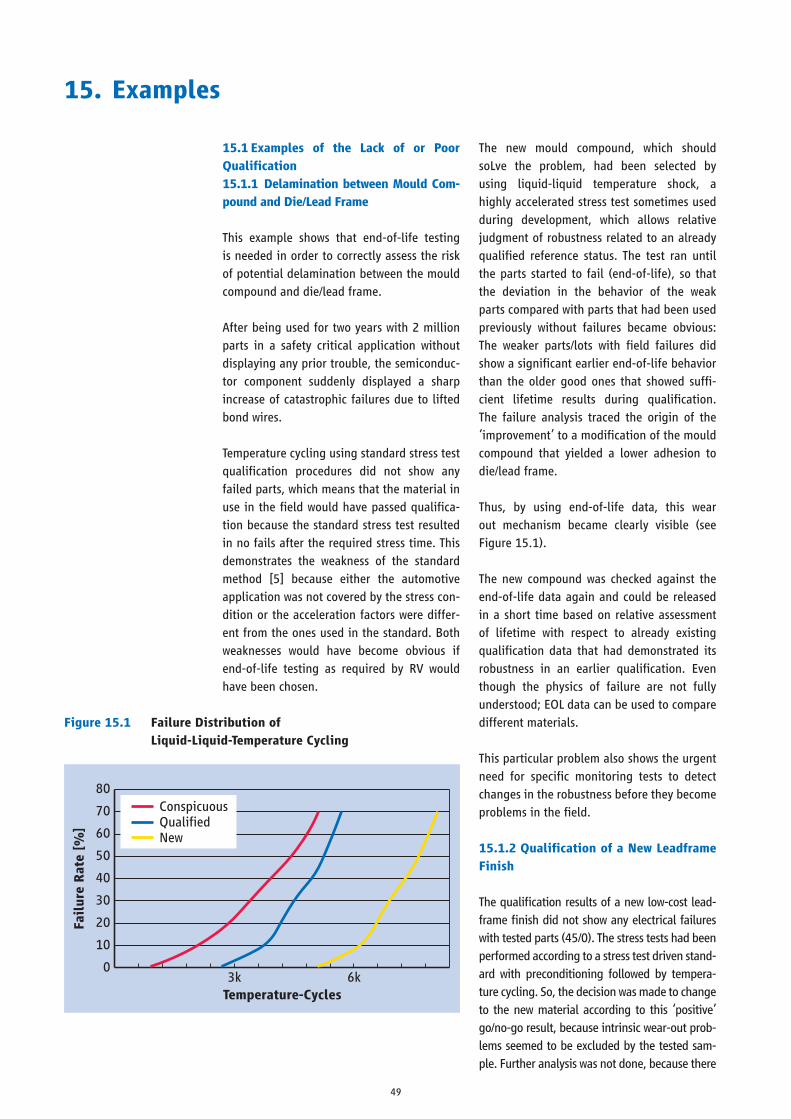
49
15. ExamplesFa
ilur
e R
ate
[%]
Temperature-Cycles
ConspicuousQualifiedNew
3k0
10
20
30
40
50
60
70
80
6k
Figure 15.1 Failure Distribution of liquid-liquid-temperature cycling
15.1 Examples of the lack of or Poor qualification15.1.1 Delamination between Mould Com-pound and Die/lead Frame
This example shows that end-of-life testing is needed in order to correctly assess the risk of potential delamination between the mould compound and die/lead frame.
After being used for two years with 2 million parts in a safety critical application without displaying any prior trouble, the semiconduc-tor component suddenly displayed a sharp increase of catastrophic failures due to lifted bond wires.
Temperature cycling using standard stress test qualification procedures did not show any failed parts, which means that the material in use in the field would have passed qualifica-tion because the standard stress test resulted in no fails after the required stress time. This demonstrates the weakness of the standard method [5] because either the automotive application was not covered by the stress con-dition or the acceleration factors were differ-ent from the ones used in the standard. Both weaknesses would have become obvious if end-of-life testing as required by RV would have been chosen.
The new mould compound, which should soLve the problem, had been selected by using liquid-liquid temperature shock, a highly accelerated stress test sometimes used during development, which allows relative judgment of robustness related to an already qualified reference status. The test ran until the parts started to fail (end-of-life), so that the deviation in the behavior of the weak parts compared with parts that had been used previously without failures became obvious: The weaker parts/lots with field failures did show a significant earlier end-of-life behavior than the older good ones that showed suffi-cient lifetime results during qualification. The failure analysis traced the origin of the ‘improvement’ to a modification of the mould compound that yielded a lower adhesion to die/lead frame.
Thus, by using end-of-life data, this wear out mechanism became clearly visible (see Figure 15.1).
The new compound was checked against the end-of-life data again and could be released in a short time based on relative assessment of lifetime with respect to already existing qualification data that had demonstrated its robustness in an earlier qualification. Even though the physics of failure are not fully understood; EOL data can be used to compare different materials.
This particular problem also shows the urgent need for specific monitoring tests to detect changes in the robustness before they become problems in the field.
15.1.2 qualification of a new leadframe Finish
The qualification results of a new low-cost lead-frame finish did not show any electrical failures with tested parts (45/0). The stress tests had been performed according to a stress test driven stand-ard with preconditioning followed by tempera-ture cycling. So, the decision was made to change to the new material according to this ‘positive’ go/no-go result, because intrinsic wear-out prob-lems seemed to be excluded by the tested sam-ple. Further analysis was not done, because there

50
seemed to be no indication of any different result compared to the zero fails from the original qual-ification performed at the first qualification with the standard frame finish.
But, additional investigations done by another party with only 18 parts as part of pre qualifi-cation work, using end-of-life tests, revealed that an unexpected metallurgy caused increased weakness of the internal stitch bond joints of the bond wires to the leadframe with a sharp incre-ase in failure-rate due to electrically open bonds after some additional stress. It could be shown that degradation had already been started at the end of the test time required by the stress test driven standard without causing an electrically detectable fail.From the data of the end-of-life test, the poten-tial failure rate in an automotive application was calculated to be in the range of 5,000 ppm.
End-of-life testing avoided a catastrophic field situation by generating Robustness Data with critical limits by using a small sample but testing until failure, which other approaches 5 were not able to reveal previously.
15.1.3 Via-Problems in Semiconductor component Metallization
After the release of a microcontroller based on a standard qualification 5, the failure rate in the field approached 1000 ppm. The failure analysis showed open vias in the IC metalliza-tion. Such opens could be caused by:• Via formulation problem
(existence of a void underneath via)• Via hole over etching
(pass through the barrier metal)• Barrier metal formulation problem
(existence of void side wall of via)
Those via problems (see Figure 15.2) lead to timing delays of transistor switching and signal. As a result, the following problems in memories occurred:• Timing delay of memory.• Read problems of memory data.• Data bus timing delay.• Miss calculation due to data timing delay.
This commercial IC was sold in millions out-side of the automotive industry with no field complaints reported.A comparison of the Mission Profile for which the IC was designed (commercial high volume, low cost) and the automotive profile showed a severe mismatch in the life expectancy of the metallization between both profiles. The weak point was the submicron via process capa-bility, which could not cover the automotive profile.Conventional stress testing did not detect this weak point based on the insufficient sample sizes needed to detect this 1000 ppm occur-rence. But end-of-life analysis on test struc-tures confirmed the missing capability for the automotive profile. The following IC was mod-ified by using a redundant double via technol-ogy in areas with sparsely populated vias and with a sufficient safety margin between the process capability and the requirement in the automotive application. As a result, no more failures happened. Because this weak point is extrinsic in nature, it cannot be detected by qualification, if it has a lower failure rate, as in this example. In this case, the main focus should be on monitoring measures.
Generally, the countermeasure activities for these problems were both reduction of parti-cle density and strengthened process control. For example:1. Process control of the critical C
pk values.
2. Test program:• Sufficient test coverage and Iddq test
blocks.• Test criteria validation.• Operation margin validation under
the condition of specification limit fre-quency and power supply voltage.
3. Electrical characteristics: The control limit should be set after the RV of static/dynamic electrical characteristics variation for each device terminal.
via
void
circuit wiring
circuit wiring
intermetal dielectric
figure 15.2 open by Void under a Via
Source: Infineon Technologies AG

51
15.2 Integrated capacitor design
Some devices need capacitors with large capacitances. They are implemented as large area capacitances using a specific dielectric as the isolator and are implemented into the interconnect part of the device structure. The reliability assessment using the knowledge base uses the following steps:1. The following data must be generated
within requirements management:• Voltage at the capacitor• Junction temperature during use• Effective time of use (duty cycle)• Capacitor area needed• Safety margin for intrinsic break down
2. The potential risk and failure mechanism for capacitors is the hard breakdown of the dielectric.
3. The information for the Qualification Plan can be extracted from the knowledge base:• Test structure design large area capacitor.• Parameter for characterization leakage
current.• Degradation model
- Percolation model• Acceleration model
- Linear E-field for voltage - Arrhenius for temperature - Area scaling with poisson distribution
4. Tests must be performed according to the description in JP001.01. The basic model data are usually measured during technol-ogy development and qualification. For a new product, these numbers could be used to calculate the expected intrinsic failure rate for the capacitor area planned includ-ing the intended safety margin, typically in terms of lifetime. Robustness areas could be defined for:• Capacitor area vs. lifetime (E, T const)• Capacitor area vs. electrical field (T, life-
time const)• Electrical field vs. lifetime (A, T const)
- The extrinsic fail distribution is domi-nated by defects. Therefore, especially for large area structures, the defect density must be kept under control in production by monitoring. First, data to guarantee a certain upper level for the extrinsic distribution could
be generated during reliability qual-ification stress testing. Monitoring of extrinsic defects should be part of the monitoring plan.
15.3 requirement temperature cycles
Different points of use in the car have different requirements with respect to the number and the ΔT of temperature cycles. The following steps describe how to cover this topic within RV:1. Requirements management delivers
the Mission Profile. Example of a typ-ical IC for an air-conditioning system: 9000 cycles with ΔT = 110 °C 7500 cycles with ΔT = 80 °C 3000 cycles with ΔT = 70 °C
2. From the Knowledge Matrix, we learn that a certain set of failure modes, such as bro-ken bond wire and solder fatigue, is gen-erated by this stress.
3. The most effective test structure to evaluate this failure mode is the assembled IC. For extrapolation from stress to operating condi-tions, the Coffin-Manson model is used.
4. Acceleration factor: AF = (ΔTstress
/ΔTuse
)p
5. If the Coffin-Manson constant p is known from experiments, it is possible to calcu-late the required number of cycles at a certain ΔT
stress (here -40 °C to +140 °C, ΔT
= 180 °C), which are needed to cover the three conditions from 1. This number plus the safety margin is the target. T
max and T
min should not be in a
parameter range where new or not appli-cation relevant failure mechanisms may be activated. Table 15.1 gives information about how the use conditions are trans-ferred into stress condition for two failure modes (the assumption is that these num-bers have been measured for the material and process used):• Al wire bond fracture: p = 5• Delamination: p = 4.2

52
The stress test must be performed accord-ing to the specification in JESD22A-104 until bond fracture or delamination occurs to generate the fail distribution. If at 1600 cycles no failures can be seen, the stress can be stopped and a worst case calculation can be made based on worst case acceleration factors.
6. If the fail distribution lies beyond the target value, the product is robust in the required application condition.
15.4 Power Electronics Design
How can the semiconductor industry actively contribute to a reliable hardware design by providing information of the aging properties of their components? An example is given for the field of Power Electronics.
15.4.1 Typical Construction of a Power MoS Device
A cross section of a typical commercially avail-able power MOS is shown in Figure 15.3.The die is mounted on a Cu leadframe. At the die surface the gate and source contact is con-nected via aluminium bond wires. The back-side of the die serves as drain contact and is connected to the Cu-leadframe via a soft sol-der die attach. The chip is encapsulated with a plastic moulding compound.
15.4.2 physics of failure
The power MOS component consists of sev-eral materials with different Coefficients of Thermal Expansion (CTE). During temperature cycles this CTE mismatch leads to shear strain and also to tensile strain at the soft solder die attach as shown in Figure 15.4. During ther-mal cycles this soft solder die attach suffers from plastic deformation and crack propaga-tion.
Figure 15.4 Schematic Cross Section Showing the Effect of Shear Strain and tensile Strain [17]
Table 15.1 example of oeM Vehicle Mission profile parameters – (high level)
Figure 15.3 cross Section of a power MoS component [16]
Δt [°c] Cycles (use) cycles (Δtstress
) (Δtstress
)
110 9,000 1,137 767
80 7,500 249 130
70 3,000 57 27

53
Figure 15.5 cracks in the die Attach due to Accumulated damage during thermal cycling [17]
The accumulation of damage during thermal cycling can result in significant delamination between the die backside and the lead frame as shown in Figure 15.5.
15.4.3 Impact of Die Attach Degradation on Thermal Management of a Power MoS
In Figure 15.6 the thermal response of a power MOS component is shown for various heating times with a given power. The ther-mal response is significantly depending on the heating time. For very short time periods the thermal capacity of the component can buffer the heat unless it will be transferred to the heat-sink to which the leadframe is connected. For longer heating times the ther-mal resistance is statically limited by heat conduction from the chip through the die attach, through the leadframe to the heat-sink. Between these two extremes, the transi-tion regime is dominated by the properties of the die attach itself. The die attach connects the die to the leadframe, which has a signif-icant thermal mass. Once this connection is disturbed (i. e. by cracks in the die attach of an aged component) the rise of the thermal response curve will occur at shorter heating times. In addition the thermal conduction is significantly reduced; therefore the saturation temperature is significantly higher compared to a new component.
Figure 15.6 Deterioration of Thermal Response as Function of the Heating time for a new and an Aged device [18]
These thermal properties can be character-ized for new but also for aged components. Depending on the thermal cycling load in a respective application, the deterioration of the thermal properties has to be taken into account. This can be done by a proper hard-ware design, selecting a component that will fulfil the thermal requirements during the ser-vice life of the application.
15.4.4 Degradation Model
To evaluate how much a component will degrade during the service life under applica-tion conditions a degradation model has to be applied. It allows calculating the equivalent stress in terms of qualification test duration based on the expected application conditions in the field.

54
For soft solder die attach, low cycle fatigue by cyclic accumulation of plastic deformation is a widely known degradation mechanism [19]. The number of cycles to fail (CTF) can be expressed as in formula (15.1) with A0 acts as a constant and q is the Coffin Manson Exponent, which is a specific to the degradation mechanism and typically material dependent. For ductile mate-rials the such as soft solder materials the Coffin Manson exponent ranges from 1 < q < 3 [20]
CTF = Ao (ΔT)-q (15.1)N2 = N
1(ΔT
1/ΔT
2)-q (15.2)
With formula (15.1) the acceleration can be calculated and expressed in formula (15.2) whereas N1 represents the number of temper-ature cycles at temperature T
1 and N2 for T
2
respectively.
By knowing the expected temperature cycling load of the component in the application the equivalent stress can be expressed in numbers of temperature cycles under qualification test conditions. By knowing the level of degrada-tion for this temperature cycling load and the impact of the components characteristics a lifetime assessment can be performed.
15.4.5 Design for lifetime Tools
In order to support the hardware engineer regarding the selection of an appropriate power MOS for his specific application, a tool would make sense which can deal with the number of thermal cycles expected in the application, and calculates the expected deterioration of the ther-mal response compared to new devices (Thermal response curve as shown in Figure 15.6).
15.4.6 Impact on Design of the Applica-tion and Impact on Component Selection Step by Step Approach
a) Mission Profile consideration on applica-tion level: Evaluation of thermal cycling load on component level. Output: Table with ΔT and amount of expected cycles in the field.
b) Calculation of equivalent damage due to the environmental load. Calculate the equivalent amount of qualification cycles for each ΔT and add these values to determine the equivalent damage based in equation (15.2) using the appropriate coefficient q.
c) Provide the thermal response curve for this damage or aging level.
d) Check if the thermal response of the aged component is still suitable for the application.
e) If not suitable, select a component with a better thermal response in initial state and go to b).
Responsibilities and deliverables: a), d), e) hardware designer of the application b) and c) component supplier

55
Appendix A – Knowledge Matrix
Appendix b – Reporting Template
The Knowledge Matrix is not intended to be and cannot be comprehensive.The current version of the Knowledge Matrix can be found on the ZVEI or SAE homepage:http://www.sae.org/standardsdev/robustnessvalidation/km.htmor http://www.zvei.org/RobustnessValidation under ‘Devices’.
It will be updated regularly independent of this document by a group of experts.Change requests should be sent to the ZVEI email address.
A template that can be used for reporting purposes is available on the ZVEI homepage.http://www.zvei.org/RobustnessValidation under ‘Implementation’.

56
For terms and definitions see corresponding fact sheet.
Appendix c – terms, definitions and Abbreviations
AEC Automotive Electronics Council
APQP Advanced Product Quality Planning
ASIC Application-Specific IC
Cl Confidence Level
Cpk
Process Capability Indes
DFMEA Design Failure Mode and Effects Analysis
DRbFM Design Review Based on Failure Mode
DRbTR Design Review Based on Test Review
DoE Design of Experiments
ECu Electronic Control Unit
EMC Electromagnetic Compatibility
EM Electro Migration
Eol End-of-Life
EoS Electrical Overstress
Fll Frequency Locked Loop
FMEA Failure Mode and Effects Analysis
GnD Ground
IC Integrated Circuit
JSAE Society of Automotive Engineers of Japan
oEM Original Equipment Manufacturer (e. g. car makers are called OEMs)
PAT Part Average Testing
PFA Physical Failure Analysis
PFMEA Process Failure Mode and Effects Analysis
Pll Phase-Locked Loop
PoR Process of Record
ppm Parts per Million
RIF Robustness Indicator Figure
RV Robustness Valdiation
SAE Society of Automotive Engineers
SbA Statistical Bin Analysis
SPC Statistical Process Control
t63 Caracteristic Lifetime
TC Temperature Cycling
TDDb Time-Dependent Dielectric Breakdown
TTF Time to Failure
ZVEIZentralverband Elektrotechnik- und Elektronikindustrie e.V.(German Electrical and Electronic Manufacturers´ Association)

57
Appendix D – References and Additional Reading
D.1 References
1. ISMI (Sematech) white paper 04024492A-TR, ‘Understanding and Developing Knowl-edge-based Qualifications of Silicon Devices’, 2004
2. JEDEC JESD91 Method for Developing Acceleration Models for Electronic Component Failure Mechanism
3. JEDEC JESD46 ‘Customer Notification of Product/Process Changes by Semiconductor Suppliers’, http://www.jedec.com
4. ZVEI Brochure, ‘Guideline for Customer Notifications of Product and/or Process Changes (PCN) of Electronic Components for Automotive Market’, 2006, http://www.zvei.org/PCN
5. Currently used stress-test-driven qualification methodology6. ZVEI Brochure, ‘Zero Defect Strategy – a joint approach all along the value chain’, 2007,
http://www.zvei.org (under ‘Publikationen’)7. JEDEC JEP 148 ‘Reliability Qualification of Semiconductor Devices Based on Physics of Fail-
ure Risk and Opportunity Assessment’, 20048. W. H. Gerling, A. Preussger, F. W. Wulfert: ‘Reliability Qualification of Semiconductor Devices
Based on Physics-of-Failure and Risk & Opportunity Assessment’, Quality and Reliability Engineering International, QREI 2002:18; 81-98
9. ‘Automotive Application Questionnaire for Electronic Control Units and Sensors’, ZVEI, 200610. W. Riordan, R. Miller, J. Sherman and J. Hicks, ‘Microprocessor Reliability Performance as a
Function of Die Location for a 0.25 mm, Five Layer Metal CMOS Logic Process’, IRPS, 199911. T. S. Barnett, A. D. Singh, M. Grady and K. Purdy, ‘Yield-Reliability Modeling: Experimental
Verification and Application to Burn-In Reduction’, Proc. 20th IEEE VLSI Test Symposium, 200212. F. Kuper, J. van der Pol, E. Ooms, T. Johnson, R. Wijburg, W. Koster and D. Johnston, ‘Relation
Between Yield and Reliability of Integrated Circuits: Experimental Results and to Continuous Early Failure Rate Reduction Program’, IRPS 1996, p. 17
13. M. Ciappa, ‘Lifetime Prediction on the Base of Mission Profiles’, ESREF 2005, p. 129314. T. T. Mattila, P. Marjamäki, L. Nguyen and J.K. Kivilahti, ‘Reliability of Chip Scale Packages under
Mechanical Shock Loading’, Electronic Components and Technology Conference, 2006, p. 58415. W. Nelson, Applied Life Data Analysis by (Wiley, 1982)16. http://www.elektroniknet.de/bauelemente/technik-know-how/leistungshalbleiter/article/64/0/
Automotive-MOSFET-Gehaeuse_fuer_bleifreie_Reflow-Loetprozesse/17. Dimosthenis C. Katsis, Thermal Characterization of Die-Attach Degradation in the power
MOSFET,Dissertation Virginia Polytechnic Institute and State University 200318. J. R. Celaya et al., Towards Prognostics of power MOSFETs: Accelerated Aging and Precursors of
Failure, Annual Conference of the Prognostics and Health Management Society, 201019. Reliability Physics and Engineering Time-To-Failure Modeling, JW McPherson PhD, Springer,
2010, ISBN978-1-4419-6347-520. JDEC Publication JEP122G
d.2 Standards related for robustness Validation
EIA-670 Quality System AssessmentISO 9001 Quality Management Systems – RequirementsJEDEC JEP70 Quality and Reliability Standards and Publications.JEDEC JEP132 Process Characterization GuidelinesJEDEC JESD34 Failure-Mechanism-Driven Reliability Qualification of Silicon DevicesJEDEC JESD659 Failure-Mechanism-Driven Reliability MonitoringJEDEC JESD94 Application Specific Qualification Using Knowledge Based Test Method-
ology

58
D.3 other Robustness Validation Documents
• Knowledge Matrix is published on ZVEI and SAE homepage (yearly update, currently 4th ver-sion under review)
• Robustness Validation for MEMS – Appendix to the Handbook for Robustness Validation of Semiconductor Devices in Automotive Applications, 2009
• Handbook for Robustness Validation of Automotive Electrical/Electronic Modules / content copy: SAE Standard J1211 (2008, under review)
• Automotive Application Questionnaire for Electronic Control Units and Sensors (2006, Daim-ler, Bosch, Infineon)
• Pressure Sensor Qualification beyond AEC Q 100 (2008, IFX: S. Vasquez-Borucki)• Robustness Validation Manual – How to use the Handbook in product engineering (2009,
RVobustness Validation Forum)• How to measure lifetime for Robustness Validation - step by step, ZVEI 2012
d.4 references discussing qualification Methodologies
• H.-P. Hoenes (Fairchild Semiconductor), ‘Powering the Future – Design and Simulation: The Key to high Reliability’, electronica automotive conference, 2006
• A. Gottschalk (RELNETyX), ‘Considerations of a Robustness Validation Procedure’, electronica automotive conference, 2006
• A. Preussger (Infineon Technologies), ‘Robustness Validation – Improved IC Qualification for Automotive Applications’, electronica automotive conference, 2006
• O. Mende (Audi), ‘ General Conditions for the successful Integration of Semiconductor Devices in Automotive Electronics’, electronica automotive conference, 2006
• E. Schmidt (BMW), ‘Targets and Requirements of Robust Automotive Electronics’, electronica automotive conference, 2006
• H. Keller and A. Preussger, ‘Robustness Validation’, Tutorial at ESREF, 2006• A. Preussger, ‘Qualification Strategies’ Tutorial at IRW, 2006• W. Kanert, ‘Qualification Strategies in the Age of Zero Defect’, AEC Reliability Workshop, 2006• W. Kanert, ‘Robustness Validation – A Short Introduction’, FIEV, 2006• W. Kanert, R. Rongen, and Z. Liang, ‘Robustness Validation’ – an Introductory Tutorial, Pro-
ceedings of AEC Reliability Workshop 2013• W. Kanert and R. Rongen, ‘Robustness Validation and Failure Rates’, Proceedings of AEC Reli-
ability Workshop 2014• W. Kanert, ‘Robustness Validation – A physics of failure based approach to qualification,
Microelectronics Reliability’, 54 (2014), 1648-1654• Position Paper (R. Winter)• Z. Liang, R. Kho, B. Bollig, R. Rongen, and F. Kuper, “Reliability Robustness Indicator Figure
and its Application”, Proceedings of AEC Reliability Workshop 2012
D.5 Standards for Analysis and Control
EIA-557 Statistical Process Control SystemsJEDEC JEP131 Process Failure Mode and Effects Analysis (FMEA)JEDEC JESD50 Special Requirements for Maverick Product EliminationJEDEC JESD671 Component Quality Problem Analysis and Corrective Action Requirements (Including Administrative Quality Problems)JEDEC JESD37 Standard for Lognormal Analysis of Uncensored Data, and of Singly Rightcensored Data Utilizing the Persson and Rootzen Method

59
D.6 Stress Test Standards
ASTM F1096-87 Measuring MOSFET Saturated Threshold VoltageASTM F1260M-96 Standard Test Method for Estimating Electromigration Median Time-To-
Failure and Sigma of Integrated Circuit MetallizationASTM F616M-96 Standard Test Method for Measuring MOSFET Drain Leakage CurrentASTM F617-00 Standard Test Method for Measuring MOSFET Linear Threshold VoltageESD STM5.1-2001 ESD Association Standard Test Method for Electrostatic Discharge
Sensitivity Testing – Human Body Model (HBM) Component LevelESD STM5.2-1999 ESD Association Standard Test Method for Electrostatic Discharge
Sensitivity Testing – Machine Model – Component LevelESD STM5.3.1-1999 ESD Association Standard Test Method for Electrostatic Discharge
Sensitivity Testing – Charged Device Model (CDM) Component LevelIPC/JEDEC J-STD-020 Moisture/Reflow Sensitivity Classification for Nonhermetic Solid State
Surface Mount DevicesJEDEC JEP122 Failure Mechanisms and Models for Semiconductor DevicesJEDEC JEP139 Constant Temperature Aging to Characterize Aluminium Interconnect
Metallization for Stress-Induced VoidingJEDEC JEP143 Solid State Reliability Assessment and Qualification MethodologiesJEDEC JESD22-A101 Steady State Temperature Humidity BiasJEDEC JESD22-A104 Temperature CyclingJEDEC JESD22-A108 Temperature, Bias and Operating LifeJEDEC JESD22-A110 Highly Accelerated Stress Test (HAST)JEDEC JESD22-A113 Preconditioning of Surface Mount Devices prior to Reliability Testing.JEDEC JESD22-A114 Electrostatic Discharge (ESD) Sensitivity Testing Human Body Model
(HBM)JEDEC JESD22-A115 Electrostatic Discharge (ESD) Sensitivity Testing Machine Mode (MM)JEDEC JESD22-C101 Field-Induced Charged-Device Model Test Method for Electrostatic-
Discharge-Withstand Thresholds of Microelectronic ComponentsJEDEC JESD28 Procedure for Measuring N-Channel MOSFET Hot-Carrier-Induced
Degradation under DC StressJEDEC JESD28-1 N-Channel MOSFET Hot-Carrier Data AnalysisJEDEC JESD33 Standard Method for Measuring and Using the Temperature Coefficient
of Resistance to Determine the Temperature of a Metallization LineJEDEC JESD35-1 General Guidelines for Designing Test Structures for the Wafer-Level
Testing of Thin DielectricsJEDEC JESD35-2 Test Criteria for the Wafer-Level Testing of Thin DielectricsJEDEC JESD35 Procedure for Wafer-Level-Testing of Thin DielectricsJEDEC JESD60 A Procedure for Measuring P-Channel MOSFET Hot-Carrier-Induced
Degradation under DC StressJEDEC JESD61 Isothermal Electromigration Test ProcedureJEDEC JESD63 Standard Method for Calculating the Electromigration Model Parame-
ters for Current Density and TemperatureJEDEC JESD74 Early Life Failure Rate Calculation Procedure for Electronic ComponentsJEDEC JESD78 IC Latch-Up TestJEDEC JESD85 Methods for Calculating Failure Rates in Units of FITsJEDEC JESD87 Standard Test Structures for Reliability Assessment of AlCu Metallization
with Barrier MaterialsJEDEC JP001 FOUNDRY PROCESS QUALIFICATION GUIDELINES (Wafer Fabrication
Manufacturing Sites)
60
Flow chart 2 (fig E1) describes (for details see Handbook for Robustness Validation of Auto-motive Electrical/Electronic Modules, ZVEI)
• (1) the process at Tier 1 to assess whether a certain electronic component fulfills the requirements of the mission profile of a new Electronic Control Unit (ECU); and
• (2) the process at Semiconductor Com-ponent Manufacturer to assess whether an existing component qualified accord-ing to AEC-Q100/101 can be used in a new application.
A detailed description of flow chart steps is given below (numbers refer to these specific flow chart steps).
E.1 Assessment on ECu level
1.1 Items to consider in constructing a Mis-sion Profile Assessment:• Type of application• Requirements of service life and usage • Environmental conditions / Mounting loca-
tion • Construction of the ECU• Power Dissipation of ECU and components• Reliability requirements in terms of lifetime
and related failure probabilities
A structured analysis of the mission profile will identify potential reliability risks in an early stage of development cycle, so that these risks can be addressed by appropriate component selection and validation.
1.2 Translation of ECU mission profile to com-ponent mission profiles, taking different load-ing on component level into account. Loads could be caused by assembly, shipping, stor-age, operation or environment. Vehicle ser-vice life is typically split into operating and non-operating parts.
1.3 Performance of ‘basic calculation’ facili-tate the mission profile assessment via a high level check of the suitability of a component (or list of components) for the given applica-tion.
These calculations enable the translation from the component mission profile to equivalent qualification test duration under specified conditions. The decision to be made here is strategic.
• Chose no if already known that product is marginal or critical.
• Chose ‘yes’ for uncritical product e.g. with references to already qualified products and being not at the extremes of its specifica-tion.
1.4 By applying the ‘basic calculation’, the mission profile is translated into an equivalent stress with the same conditions as the quali-fication standard test. Commonly accepted acceleration models and parameters are used and can be taken from the literature and/or standards (e. g. JEP122). Examples are given in table 9.1.
1.5 This calculated stress duration tCALC
(in hours or number of cycles) has to be com-pared to the standard qualification duration tSTAND
, taking a safety margin tSM
into account.
1.6 In case tSTAND
> tCALC
+ tSM
, the component is assumed to be not critical/marginal. The safety margin tSM has to be defined based on the application and customer requirements; there are no standardized rules for this. Assessment of criticality shall include the probability of failure until end-of-life.
e.2 Mission profile Validation on com-ponent level
2.1 The recommended base for assessing the critical failure mechanism(s) is the Robustness Validation Knowledge Matrix or JEP122. Risk assessment should be performed covering at least the following main considerations:
• New materials or interfaces• New design or production techniques• Critical use conditions
Appendix e – relation to Aec-q100/101 for already qualified electronic components

61
Methods for risk assessment could be FMEA (AIAG, …), Risk Assessment, FTA or similar.
2.2 In case acceleration models are in use in the company or known from the literature, they can be taken to perform lifetime calcu-lations. Experiments, simulation, or literature study can be used to create such acceleration models. Sufficient acceleration may be impos-sible due to limiting physical boundary con-ditions. In such a case minimum stress times should be defined to demonstrate sufficient robustness margin, (e. g., based on change or degradation of any electrical or physical prop-erties during or after stress and the impact on the specific application).
2.3 The acceleration model is used to calculate the acceleration factor for the standard stress condition. This in return gives the calculated minimum required stress time t
CALC (in hrs or
number of cycles) to demonstrate reliability without failures.
2.4 A comparison with the standard qualifi-cation duration t
STAND is to be made. In case
tSTAND
> tCALC
, the component is assumed to be not critical/marginal. The robustness margin t
SM has to be defined based on the application
and customer requirements. Assessment of criticality shall include the accumulated fail-ure probability until end-of-life. Criteria for a decision shall include not only test conditions and durations as compared to the standard, but also coverage of critical failure mecha-nisms by the tests. Such coverage consider-ations include applicability of assumptions used in calculating the stress conditions, such as variation of the activation energy for differ-ent failure mechanisms. Beyond that it has to be assessed, if particular failure mechanisms are addressed by the standard test method at all. A case in point is active cycling of power devices, which is not adequately addressed by standard qualification tests. In addition, spe-cific requirements regarding fail probabilities may not be covered by standard test proce-dures. MIM capacitors, for instance, are known to fail due to extrinsic defects. A requirement of, e.g., less than 100 ppm for extrinsic fail-ures will not be covered by standard tests and sample sizes.
2.5a Based on the calculations in 2.3 the mission profile is more severe than the AEC-Q100 test conditions. In this case test condi-tions have to be defined which are equivalent or more severe than the mission profile. This can either be a longer test time or harsher test conditions such as higher temperatures. Both based on the acceleration models evaluated under 2.2. This means that more severe test conditions are applied for the product qual-ifications than the conditions defined in the AEC Q100.
2.5b If qualification data with the required test conditions are not available, it has to be decided if the qualification test data can be generated by the component supplier with reasonable effort.
2.6 Once the test conditions are defined, the technical feasibility has to be evaluated. On product level there are limitations regarding maximum temperatures, voltages or currents which can be applied. Therefore the level of lifetime acceleration is limited. In cases a rea-sonable product qualification scenario cannot be identified, another approach has to be applied. In this case the capability of the tech-nology and the design of a component have to be evaluated specifically based on the tech-nology lifetime characterization acc. to the Robustness Validation process.
B: Testing must be performed according to mission profile specific test conditions.
E.3 Robustness Validation on Compo-nent level
3.1 In case of capability of a component for a given mission profile cannot be achieved until step 2.6, the use of more capable alternative components should be considered. If alterna-tive components with higher robustness are not available either the mission profile has to be adopted or the technological capability of the component has to be assessed applying the robustness validation approach.
C: Testing must be performed according to mission profile requirements following the Robustness Validation strategy with focus on

62
critical failure mechanisms. The test plan shall be aligned between CM and Tier 1.
Process for qualification plan generation based on mission profile:a) List all conditions, operating, non-operat-
ing, production or transport with all rel-evant parameters like temperature, tem-perature cycles, humidity or other and the correspondent time the condition applies.
b) For a temperature mission profile all peri-ods with identical temperatures are sum-marized. An example for one condition of
a temperature mission profile is given in line 1 of table E.1. For a predefined stress condition each of the conditions can be quantified using the acceleration model, here the Arrhenius model. The result is the equivalent stress time.
c) For a temperature cycling and a humidi-ty-temperature example the calculation is shown in line 2 and 3 using the Cof-fin-Manson and Hallberg-Peck model.
Table E1 examples for calculating test durations based on single conditions from Mission profile
loading Missionprofile Input
Stress Test StressConditions
Acceleration Model(all temperatures in K,
not in °c)
Model Parameters Calculated Test Duration
one opera-tional mode
tu = 2,000 h
(single mode operating use)
Tu = 87 °C
(single mode related junction temperature in use environ-ment)
HighTemperature OperatingLife(HTOL)
Tt = 125 °C
(junction tem-perature in test environment)
Arrhenius
Also applicable for High Temperature Storage Life (HTSL) and NVM Endurance, Data Retention Bake, & Operational Life (EDR)
Ea = 0.7 eV
(activation energy; 0.7 eV is a presumed value, actual values depend on failure mechanism and range from -0.2 to 1.4 eV)
kB = 8.61733 x 10⁻⁵ eV/K
(Boltzmann’s Constant)
tt = 232 h
(test time)
Thermo-mechanical
nu = 54,750 cls
(number of engine on/off cycles over 15 yr of use)
∆Tu =76 °C
(average thermal cycle temperature change in use environment)
Temperature Cycling(TC)
∆Tt =205 °C
(thermal cycle temperature change in test environment: -55 °C to 150 °C)
Coffin Manson
Also applicable for Power Temperature Cycle (PTC)
m = 4(Coffin Manson exponent; 4 is a presumed value and to be used for cracks in hard metal alloys, actual values depend on failure mechanisms and range from 1 for ductile to 9 for brittle materials)
nt =1034 cls
(number of cycles in test)
Humidity&
Temperature
tu = 3,000 hr
(engine off time over 15 yr of use)
RHu = 91 %
(average relative humidity in use environment)
Tu = 27 °C
(average tem-perature in use environment)
Temperature HumidityBias(THB)
RHt = 85 %
(relative humidity in test environ-ment)
Tt = 85 °C
(ambient tem-perature in test environment)
Hallberg-Peck
Also applicable for Highly Accelerated Steam Test (HAST) and Unbiased Humid-ity Steam Test (UHST).See (Note)s.
p = 3(Peck exponent, 3 is a pre-sumed value and to be used for bond pad corrosion)
Ea = 0.8 eV
(activation energy; 0.8 eV is a presumed value)
kB = 8.61733 x 10⁻⁵ eV/K
(Boltzmann’s Constant)
Tt = 24.5 h
−•=
tuB
af
TTkEA 11exp
f
ut
Att =
m
u
tf
TTA
∆∆
=
f
ut
Ann =
−••=
tuB
a
u
t
p
fTTk
ERHRHA 11exp
f
ut
Att =

63
loading Missionprofile Input
Stress Test StressConditions
Acceleration Model(all temperatures in K,
not in °c)
Model Parameters Calculated Test Duration
one opera-tional mode
tu = 2,000 h
(single mode operating use)
Tu = 87 °C
(single mode related junction temperature in use environ-ment)
HighTemperature OperatingLife(HTOL)
Tt = 125 °C
(junction tem-perature in test environment)
Arrhenius
Also applicable for High Temperature Storage Life (HTSL) and NVM Endurance, Data Retention Bake, & Operational Life (EDR)
Ea = 0.7 eV
(activation energy; 0.7 eV is a presumed value, actual values depend on failure mechanism and range from -0.2 to 1.4 eV)
kB = 8.61733 x 10⁻⁵ eV/K
(Boltzmann’s Constant)
tt = 232 h
(test time)
Thermo-mechanical
nu = 54,750 cls
(number of engine on/off cycles over 15 yr of use)
∆Tu =76 °C
(average thermal cycle temperature change in use environment)
Temperature Cycling(TC)
∆Tt =205 °C
(thermal cycle temperature change in test environment: -55 °C to 150 °C)
Coffin Manson
Also applicable for Power Temperature Cycle (PTC)
m = 4(Coffin Manson exponent; 4 is a presumed value and to be used for cracks in hard metal alloys, actual values depend on failure mechanisms and range from 1 for ductile to 9 for brittle materials)
nt =1034 cls
(number of cycles in test)
Humidity&
Temperature
tu = 3,000 hr
(engine off time over 15 yr of use)
RHu = 91 %
(average relative humidity in use environment)
Tu = 27 °C
(average tem-perature in use environment)
Temperature HumidityBias(THB)
RHt = 85 %
(relative humidity in test environ-ment)
Tt = 85 °C
(ambient tem-perature in test environment)
Hallberg-Peck
Also applicable for Highly Accelerated Steam Test (HAST) and Unbiased Humid-ity Steam Test (UHST).See (Note)s.
p = 3(Peck exponent, 3 is a pre-sumed value and to be used for bond pad corrosion)
Ea = 0.8 eV
(activation energy; 0.8 eV is a presumed value)
kB = 8.61733 x 10⁻⁵ eV/K
(Boltzmann’s Constant)
Tt = 24.5 h
Figure E1 flow chart 2 – reliability test criteria for qualified component
B
A
No
Robustness Validationon Component Level
* Note that this flow chart does not coverthe consideration of AEC acceptance criteriabased on LTPD-sampling plan (max. of 1%failures allowed) versus the RobustnessValidation failure rate extrapolation
Tier 1 +CMCM
Additionaldata can
be created?
2.6 Yes
2.5b
Assessment of available qualification data against a specificmission profileProcess at Tier 1:Assess whether a certain electronic component fulfills the requirements of themission profile of a new ECUProcess at Component Manufacturer (CM):Assess whether an existing component qualified according to AEC-Q101 testconditions fulfills the requirements of the mission profile of a new application
Responsibility
Tier 1
Determine mission profileof the componentincluding loading
Determine critical FailureMechanisms
Calculate test durationwith standard accelerationmodels for standard tests
and test conditions
Calculate test durationwith selected accelerationmodels for standard tests
and test conditions
AEC-Q101 test conditionsexceed / are sufficient*
Mission Profilevalidated*
Yes
No
Yes
No
Yes
Mission Profile Validation on Component Level
Alternativecomponent?
Additionaldata
available?
No
Yes
Assessment on ECU level
Basiccalculation?
More severethen AEC-
Q101?
No
Perform RobustnessValidation with
detailed alignmentbetween SCM andTier 1 on mission
profile and/or criticalfailure mechanisms*
No
1.1
1.2
1.3
1.4
1.5
1.6
2.1
2.2
2.3
2.4
2.5a
3.1
C
Determine Mission Profileon ECU level
Compare with AEC-Q101test conditions
Determine accelerationmodels
Critical/Marginal
Yes
Yes
No
YesCritical/Marginal?

64
In this example the distribution of temperature stress over the lifetime, the temperature mission profile of the component is shown in figure F1.
A conservative approach for a failure mechanism associated with high temperature would be to link each bin to its maximum temperature. In this case this would result in the values given in table F1.
For two failure mechanisms:1. FM1: transistor degradation (Vt-shift) due to H2 diffusion thru silica with Ea = 0.42 eV2. FM2: short due to Cu diffusion with Ea = 1.0 eV
and using Arrhenius equation the contribution to a stress time at 150 °C could be calculated for each of the four temperatures (see tab F2).
Appendix f – from Mission profile to test condition(an example)
Figure F1 temperature Mission profile
Duration (h) percentage (%) tj component (°c)
1000 10 48
1600 16 71
6500 65 108
890 9 150
Table F1 Mission profile example
Duration (h) tj component (°c) Stress duration(h for FM1)
Stress duration(h for fM2)
1000 48 27 0.2
1600 71 114 3
6500 108 1826 316
890 150 890 890
Stress equivalent/sum 150 2857 1209
table f2 Stress time equivalent per temperature in Mission profile
0 20 40 60 80 100 120 140 160 180
7000
6000
5000
4000
3000
2000
1000
Operation time* [h]
Tj [°C]-40 -20

65
The resulting cumulative stress time for 150 °C is 2857 h for failure mechanism 1 and is 1209 h for failure mechanism 2. These stress times are representing the load for all four temperatures under use conditions.
The range of activation energies for typical temperature related failure mechanism is between -0.2 eV and 1.4 eV. Figure F2 demonstrates the effect of activation energies on acceleration factors that are used for life and stress time calculation.
It should be noted that the acceleration factor from 48 °C to 150 °C changes be 7 orders of magnitude for the range of typical activation energies. For acceleration from 108 °C to 150 °C the change is still 2 orders of magnitude. This means that wrong assumptions for the critical failure mechanism and related activation energy could result in severly wrong life time forecast.
figure f2 Acceleration Factor vs Activation Energy
use at 108°Cstress at 150°C
Activation Energy Ea (eV)
use at 48°Cstress at 150°C
Acce
leratio
n Fa
ctor
AF
1.61.21 1.40 0.2 0.4 0.6 0.8
0.1
1.0
10.0
100.0
1,000.0
10,000.0
100,000.0
1,000,000.0
-0.4 -0.2
66
notes

German Electrical and Electronic Manufacturers‘ Association Electronic Components and Systems Division Lyoner Straße 9 60528 Frankfurt am Main, Germany
Phone: +49 69 6302-402 Fax: +49 69 6302-407 E-mail: [email protected] www.zvei.org www.zvei.org/robustnessvalidation
Bild
nach
wei
s: T
itel
: © A
rchM
en –
Fot
olia
.com