Guideline for PSSE Stability Modeling of ... - ngus.force.com
17
Version 1 4/30/2021 1| Page Guideline for PSSE Stability Modeling of Inverter-Based DER ≥ 5 MW to Meet National Grid SRD for Western RI DER ASO 3 (applicable to PSSE V34) The following generic renewable energy system modules from the PSS/E Rev 34.8.1 Standard Library models shall be used to represent the transient stability characteristics of the inverter-based DERs. 1.) Renewable Energy Generator/Converter Model: REGC_B 2.) Renewable Energy Electrical Model: REEC_D 3.) Power Plant Controller model: REPC_A -- (for Stand-Alone PV, Stand-Alone BESS, and DC coupled PV+BESS) PLNTBU1 + REAX4BU1 – (For AC coupled PV+BESS) The sections below provide guidelines for parameterizing these generic PSS/E renewable energy system models to comply with various performance requirements outlined in the Source Requirements Document (SRD) for the Western RI DER ASO 3 Study (refer to National Grid SRD_Western RI ASO3.pdf).
Transcript of Guideline for PSSE Stability Modeling of ... - ngus.force.com

Version 14/30/2021
1 | P a g e
Guideline for PSSE Stability Modeling of Inverter-Based DER ≥ 5 MW
to Meet National Grid SRD for Western RI DER ASO 3(applicable to PSSE V34)
The following generic renewable energy system modules from the PSS/E Rev 34.8.1 Standard Library
models shall be used to represent the transient stability characteristics of the inverter-based DERs.
1.) Renewable Energy Generator/Converter Model:
REGC_B
2.) Renewable Energy Electrical Model:
REEC_D
3.) Power Plant Controller model:
REPC_A -- (for Stand-Alone PV, Stand-Alone BESS, and DC coupled PV+BESS)
PLNTBU1 + REAX4BU1 – (For AC coupled PV+BESS)
The sections below provide guidelines for parameterizing these generic PSS/E renewable energy system
models to comply with various performance requirements outlined in the Source Requirements
Document (SRD) for the Western RI DER ASO 3 Study (refer to National Grid SRD_Western RI ASO3.pdf).

Version 14/30/2021
2 | P a g e
REGC_B Model Guidelines - Model parameters are to be provided in per unit of machine MVA base.
Parameter DescriptionTypical Value
or range ofValues*
Comments
RateFlagRateFlag switch;0: rate limit on active current,1: rate limit on active power
0 or 1 Inverter specific
PQ PriorityFlag
PQ priority Flag;0: Q priority,1: P priority
0 or 1
Needs to be consistent with the PQFlag ofassociated REEC_D model
Set to 0 (Q Priority), if providing dynamicvoltage support in the mandatory operationregion of attached SRD document
Set to 1 (P Priority), if not providing dynamicvoltage support in the mandatory operationregion of attached SRD document
TgLag time constant emulating currentregulator response time. [s]
0.017 to 0.03 Cannot be zero
TeLag time constant representing delayin converter firing controls. [s].
0.01 to 0.017 Should generally not set this to zero
TfltrLag time constant representing the lagin the terminal voltage measurementtransducer [s]
0.02 to 0.05 Can be set to zero
Rrpwr
Rate limit on active power recoveryrate after a large voltage dip, orsudden change in active powercommand. [p.u/s]
2 to 20
Ramp rate for active current recovery needsto be at least 2 p.u/s since IEEE 1547requires DERs to restore output to at least80% within 0.4 seconds. Please provide theinverter’s actual ramp rate.
Re Equivalent source resistance. [p.u] 0 to 0.02
Re is a Loadflow model parameter, not astability model parameter. Please provideseparately in the load flow model.Re is typically set to zero
Xe Equivalent source reactance. [p.u] 0.05 to 0.3
Xe is a Loadflow model parameter, not astability model parameterPlease provide separately in the load flowmodel.
Iqrmax
Rate limit on reactive current recoveryafter a fault if the initial reactivecurrent is positive (injecting into thegrid).
1 to 999
Parameter value is irrelevant because initialreactive current is always zero (DER notallowed to control voltage under normaloperating conditions (i.e. “steady state)
Iqrmin
Rate limit on reactive current recoveryafter a fault if the initial reactivecurrent is negative (absorbing fromthe grid).
-1 to -999
Parameter value irrelevant because initialreactive current is always zero (DER notallowed to control voltage under normaloperating conditions (i.e. “steady state)
Imax Maximum converter current limit [p.u] 1.0 to 1.5
Needs to be consistent with the associatedREEC_D modelPlease provide inverter’s maximum currentcapability.
*Typical values are provided only for guidance and should not be interpreted as a strict range of
numbers.

Version 14/30/2021
3 | P a g e
REEC_D Model Guidelines - Model parameters are to be provided in per unit of machine MVA base.
Parameter DescriptionTypical Value
or range ofValues*
Comments
PFFLAG• 1 if power factor control• 0 if Q control (which can be controlledby an external signal)
0 or 1Set to 0. DERs not allowed to controlvoltage under normal operating conditions.
VFLAG• 1 if Q control• 0 if voltage control
0 or 1Set to 0 or 1. VFLAG value is irrelevant ifQFLAG is set to zero
QFLAG• 1 if voltage or Q control• 0 if constant pf or Q control
0 or 1Set to 0. DERs not allowed to controlvoltage under normal operating conditions
PFLAG• 1 if active current command has speeddependency• 0 for no dependency
0 or 1Set to 0. No speed dependency for PV orBESS.
PQFLAGP/Q priority flag for current limit:• 0 for Q priority• 1 for P priority
0 or 1
Needs to be consistent with PQFlag ofassociated REGC_B model
Set to 0 (Q Priority), if providing dynamicvoltage support in the mandatory operationregion of attached SRD document
Set to 1 (P Priority), if not providing dynamicvoltage support in the mandatory operationregion of attached SRD document
VcmpFlag:• 1 for current compensation• 0 for reactive droop compensation
0 or 1Setting is irrelevant, since Qflag set to 0.DERs not allowed to control voltage undernormal operating conditions.
Vdip (pu)low voltage threshold to activatereactive current injectionlogic
<0.90
Set to 0.88pu, if providing dynamic voltagesupport in the low voltage, mandatoryoperation region of attached SRD document
Set to < 0.50, if not providing dynamicvoltage support in the low voltage,mandatory operation region of attachedSRD document
Vup (pu)Voltage above which reactive currentinjection logic is activated
> 1.10Set above 1.2 so as not to provide dynamicvoltage support in the continuous operationregion of attached SRD document
Trv (s) Voltage filter time constant 0.02 to 0.05Inverter specific. Needs to be the same asTfltr in REGC_B model.
dbd1 (pu)Voltage error dead band lowerthreshold (≤0)
-0.1 to 0Enter inverter specific values if inverter isproviding dynamic voltage support in in thelow voltage, mandatory operation region ofattached SRD document.
Otherwise, parameter values are irrelevant.
dbd2 (pu)Voltage error dead band upperthreshold (≥0)
0 to 0.1
Kqv (pu)Reactive current injection gain duringover and undervoltage conditions
0 to 10
Iqh1 (pu),Upper limit on reactive current injectionIqinj
1 to 1.1

Version 14/30/2021
4 | P a g e
Parameter DescriptionTypical Value
or range ofValues*
Comments
Iql1 (pu),Lower limit on reactive current injectionIqinj
-1.1 to 1
Vref0 (pu),User defined reference (if 0, modelinitializes it to initial terminal voltage)
0.95 to 1.05
IqfrzValue to which reactive-currentcommand is frozen after a voltage-dip[p.u]
0
Thld
Time for which reactive-currentcommand is frozen after a voltage-dip[s]; if positive then Iqcmd is frozen to itsfinal value during the voltage-dip; ifnegative then Iqcmd is frozen to Iqfrz
0
Thld2Time for which Ipcmdbl (value of Ipcmdbefore limit) is frozen after the voltagedip is over (s)
0 inverter specific
TpFilter time constant for electrical power(s),
0.01 to 0.1 inverter specific
QMaxThe maximum value of the incomingQext or Vext [p.u]
0.4 to 1.0Set to 0. Inverter not allowed to controlvoltage under normal operating conditions
QMinThe minimum value of the incomingQext or Vext [p.u]
-1.0 to -0.4Set to 0. Inverter not allowed to controlvoltage under normal operating conditions
VMAX Maximum limit for voltage control [p.u] 1.05 to 1.1
Parameter values are irrelevant, since QFlagset to 0. DERs not allowed to controlvoltage under normal operating conditions
VMIN Minimum limit for voltage control [p.u] 0.9 to 0.95
KqpReactive power regulator proportionalgain (p.u)
N/A
KqiReactive power regulator integral gain(p.u)
N/A
KvpVoltage regulator proportional gain(p.u)
N/A
Kvi Voltage regulator integral gain (p.u) N/A
Vbias User-defined bias (p.u) normally 0Parameter value irrelevant, since VFlag setto 1.
Tiq Time constant on delay for block s4 (s) 0.02 – 0.05 inverter specific
dPmaxPower reference maximum ramp rate(p.u/s)
>0 Must be greater than 0
dPminPower reference minimum ramp rate(p.u/s)
<0 Must be less than 0
PMAX Maximum power limit (p.u) 1
PMIN Minimum power limit (p.u) 0
ImaxMaximum limit on total convertercurrent (p.u)
1.0 to 1.5 Must match Imax value in REGC_B model
Tpord Power filter time constant (s) 0.02 to 0.05
VDL vq-iq10 pairs of values defining the voltagedependent reactive-current limits [p.u]
N/A
Enter Inverter specific values if inverteremploys Voltage Dependent Limits forreactive current. Otherwise, set all VDL vq-iqdata to zero
VDL vp-ip10 pairs of values defining the voltagedependent active-current limits [p.u]
N/A
Enter Inverter specific values if inverteremploys Voltage Dependent Limits for activecurrent. Otherwise, set all VDL vp-ip data tozero

Version 14/30/2021
5 | P a g e
Parameter DescriptionTypical Value
or range ofValues*
Comments
rc Current-compensation resistance [p.u] 0 to 0.02
Parameter values are irrelevant, since QFlagset to 0. DERs not allowed to controlvoltage under normal operating conditions
Xc Current-compensation reactance [p.u] 0.01 to 0.12
Tr1Filter time constant for voltagemeasurement. Can be set to “zero”. [s]
0.02 to 0.05
Kc Reactive-current compensation gain 0.01 to 0.05
Ke Scaling on Ipmin; 0 to 1set to 0 for a generator,set to a value between 0 and 1 for a storagedevice, as appropriate
vblklVoltage below which the converter isblocked (i.e. Iq = Ip = 0)
0.50 p.uSet to 0.50 p.u to correctly modelMomentary Cessation low voltage thresholdper attached SRD document
vblkhVoltage above which the converter isblocked (i.e. Iq = Ip = 0)
1.1 p.uSet to 1.10 p.u to correctly modelMomentary Cessation high voltagethreshold per attached SRD document
Tblk_delayThe time delay following blocking of theconverter after which the converter isreleased from being blocked
0.04 to 0.1Time delay after release from converterblocking due to Momentary cessation.
*Typical values are provided only for guidance and should not be interpreted as a strict range of numbers.
Where N/A is listed, this indicates that there is no typical range to be provided.

Version 14/30/2021
6 | P a g e
REPC_A Model Guidelines – To be used for stand-Alone PV, stand-Alone BESS, and DC coupled
PV+BESS
Model parameters are to be provided in per unit of machine MVA base.
Parameter DescriptionTypical Value
or range ofValues*
Comments
VCFLAG Droop flag for Voltage control 0 or 1 Set to 0 or 1. Irrelevant if RefFlag is set to 0
RefFlag Flag for Voltage or Q control 0 or 1Set to 0. No voltage control allowed forcontinuous operation.
Fflag Frequency Control Flag 0 or 1Set to 1, Enable frequency response, perattached SRD document
tfltrVoltage and reactive power filtertime constant, sec.
0.02 to 0.05
Parameter values are irrelevant, DERs notallowed to control voltage under normaloperating conditions
kpVolt/VAr regulator proportionalgain, p.u.
-
kiVolt/VAr regulator integral gain,p.u.
-
tftPlant controller Q output lead timeconstant, sec.
0
tfvPlant controller Q output lag timeconstant, sec.
0.02 to 0.15
vfrzVoltage for freezing Volt/VArregulator integrator, p.u.
0.00 to 0.90
rcLine drop compensationresistance, p.u.
0.0
xcLine drop compensation reactance,p.u.
0.0
kc Reactive droop gain, p.u. -
emax Maximum Volt/VAr error, p.u. -999
emin Minimum Volt/VAr error, p.u. 999
Dbd1Lower threshold for reactive powercontrol deadband (<=0)
<=0
Dbd1Upper threshold for reactive powercontrol deadband (>=0)
>=0
QmaxMaximum plant reactive powercommand, p.u.
0.00 to 0.43Set to 0. No voltage control allowed forcontinuous operation
QminMinimum plant reactive powercommand, p.u.
-0.43 to 0.00Set to 0. No voltage control allowed forcontinuous operation.
kpgReal power control proportionalgain, p.u.
- PPC specific
kigReal power control integral gain,p.u.
- PPC specific
tpActive power filter time constant,sec.
0.02 to 0.05 PPC specific
fdbd1Frequency deadband downside,p.u.
-0.01 to 0.00Set to - 0.0006 p.u. 0.036 Hz deadband isrequired per attached SRD (0.036Hz/60Hz)

Version 14/30/2021
7 | P a g e
Parameter DescriptionTypical Value
or range ofValues*
Comments
fdbd2 Frequency deadband upside, p.u. 0.00 to 0.01Set to 0.0006 p.u. 0.036 hz deadband isrequired per attached SRD (0.036Hz/60Hz)
femaxMaximum power error in droopregulator, p.u.
-999
feminMinimum power error in droopregulator, p.u.
999
pmaxMaximum plant active powercommand, p.u.
1
pminMinimum plant active powercommand, p.u.
0 or -1
Set to 0 if Stand-Alone PV.Set to -1 if stand-alone BESS.
If DC coupled PV+BESSSet to negative of BESS MW rating,in p.u of PV MW rating, if PV MWrating larger than BESS MW rating
Otherwise, set to – 1.
tgPlant controller P output lag timeconstant, sec.
0.02 to 0.15 PPC specific
ddnReciprocal of down regulationdroop, p.u.
0.00 to 33.33Set to 20. 5% droop setting is required perattached SRD document.
dupReciprocal of up regulation droop,p.u.
0.00 to 33.33
Set to 20 if stand-alone BESS or DC CoupledPV+BESS. 5% droop setting is required perattached SRD document.
Otherwise, set to 0.
*Typical values are provided only for guidance and should not be interpreted as a strict range of numbers.
Where N/A is listed, this indicates that there is no typical range to be provided.

Version 14/30/2021
8 | P a g e
PLNTBU1 Model Guidelines – To be used for AC coupled PV+BESS
Note: REAX4BU1 Model is also required to be used with PLNTBU1 (see later in document)
Model parameters are to be provided in per unit of system MVA base (100 MVA).
Parameter DescriptionTypical Value
or range ofValues*
Comments
VCFLAG Droop flag for Voltage control 0 or 1 Set to 0 or 1. Irrelevant if RefFlag is set to 0
RefFlag Flag for Voltage or Q control 0 or 1Set to 0. No voltage control allowed forcontinuous operation.
Fflag Freqency Control Flag 0 or 1Set to 1, Enable frequency response, perattached SRD document
tfltrVoltage and reactive power filtertime constant, sec.
0.02 to 0.05
Parameter values are irrelevant, DERs notallowed to control voltage under normaloperating conditions
kpVolt/VAr regulator proportionalgain, p.u.
-
kiVolt/VAr regulator integral gain,p.u.
-
tftPlant controller Q output lead timeconstant, sec.
0
tfvPlant controller Q output lag timeconstant, sec.
0.02 to 0.15
vfrzVoltage for freezing Volt/VArregulator integrator, p.u.
0.00 - 0.90
rcLine drop compensationresistance, p.u.
0.0
xcLine drop compensation reactance,p.u.
0.0
kc Reactive droop gain, p.u. -
emax Maximum Volt/VAr error, p.u. -999
emin Minimum Volt/VAr error, p.u. 999
Dbd1Lower threshold for reactive powercontrol deadband (<=0)
<=0
Dbd1Upper threshold for reactive powercontrol deadband (>=0)
>=0
QmaxMaximum plant reactive powercommand, p.u.
0.00 to 0.43Set to 0. No voltage control allowed forcontinuous operation
QminMinimum plant reactive powercommand, p.u.
-0.43 to 0.00Set to 0. No voltage control allowed forcontinuous operation.
kpgReal power control proportionalgain, p.u.
- PPC specific
kigReal power control integral gain,p.u.
- PPC specific
tpActive power filter time constant,sec.
0.02 to 0.05 PPC specific
fdbd1Frequency deadband downside,p.u.
-0.01 to 0.00Set to - 0.0006 p.u. 0.036 hz deadband isrequired per attached SRD (0.036Hz/60Hz)

Version 14/30/2021
9 | P a g e
Parameter DescriptionTypical Value
or range ofValues*
Comments
fdbd2 Frequency deadband upside, p.u. 0.00 to 0.01Set to 0.0006 p.u. 0.036 Hz deadband isrequired per attached SRD (0.036Hz/60Hz)
femaxMaximum power error in droopregulator, p.u.
-999
feminMinimum power error in droopregulator, p.u.
999
pmaxMaximum plant active powercommand, p.u.
N/ASet to greater of either PV or BESS MWrating, in p.u of 100 MVA base
pminMinimum plant active powercommand, p.u.
N/ASet to negative of BESS MW rating, in p.u of100 MVA base
tgPlant controller P output lag timeconstant, sec.
0.02 to 0.15 PPC specific
ddnReciprocal of down regulationdroop, p.u.
0.00 to 33.33Set to 20. 5% droop setting is required perattached SRD document.
dupReciprocal of up regulation droop,p.u.
0.00 to 33.33Set to 20. 5% droop setting is required perattached SRD document.
MVA_P Plant Controller MVA base N/ASet to 0. All p.u values in PLNTBU1 modelare to be provided on system (100 MVA)base.
*Typical values are provided only for guidance and should not be interpreted as a strict range of numbers.
Where N/A is listed, this indicates that there is no typical range to be provided.

Version 14/30/2021
10 | P a g e
REAX4BU1 Model Guidelines – To be used in conjunction with PLNTBU1 for AC coupled PV+BESS
Note: one REAX4BU1 model is required for each PV or BESS unit that are AC coupled.
Model parameters are to be provided in per unit of machine MVA base.
Parameter DescriptionTypical Value
or range ofValues*
Comments
Tw1 (s), Measurement time constant N/A Inverter specific
Kw1 (pu onMBASE),
Gain for signal in reactive path -Irrelevant, since DERs not allowed to controlvoltage under normal operating conditions
Kp1(pu onMBASE),
Gain for signal in real path N/A
Wmax (pu), Maximum value of W01 - Irrelevant, since DERs not allowed to controlvoltage under normal operating conditionsWmin (pu), Minimum value of W01 -
Pmax (pu), Maximum value of P01 1 1 if either PV unit or BESS unit
Pmin (pu), Minimum value of P01 0 or -10 if PV unit-1 if BESS unit
*Typical values are provided only for guidance and should not be interpreted as a strict range of numbers.
Where N/A is listed, this indicates that there is no typical range to be provided.

Version 14/30/2021
11 | P a g e
VTGTPAT and FRQTPAT Model Guidelines - Voltage and Frequency Trip Settings
The following parameters for voltage and frequency trip relay PSS/E models need to be used to
represent the required inverter trip settings specified in the attached SRD document.
Parameter Model Value Description
VL VTGTPAT 0.88Trip for voltages below 0.88pu for more than 3 seconds
VU VTGTPAT 999
TP VTGTPAT 3.0
VL VTGTPAT 0.5 Trip for voltages below 0.5pu for more than 1.1seconds
VU VTGTPAT 999
TP VTGTPAT 1.1
VL VTGTPAT 0Trip for voltages above 1.1pu for more than 2 seconds
VU VTGTPAT 1.1
TP VTGTPAT 2
VL VTGTPAT 0 Trip for voltages above 1.2pu for more than 0.16seconds
VU VTGTPAT 1.2
TP VTGTPAT 0.16
FL FRQTPAT 58.5 Trip for frequency below58.5 Hz for more than 300seconds
FU FRQTPAT 999
TP FRQTPAT 300
FL FRQTPAT 56.5 Trip for frequency below56.5 Hz for more than 0.16seconds
FU FRQTPAT 999
TP FRQTPAT 0.16
FL FRQTPAT 0 Trip for frequency above 62Hz for more than 0.16seconds
FU FRQTPAT 62
TP FRQTPAT 0.16
FL FRQTPAT 0 Trip for frequency above61.2 Hz for more than 300seconds
FU FRQTPAT 61.2
TP FRQTPAT 300

Version 14/30/2021
12 | P a g e
REGC_B Block Diagram [Source: PSS/E]

Version 14/30/2021
13 | P a g e
REEC_D Block Diagram [Source: PSS/E]

Version 14/30/2021
14 | P a g e
REEC_D Block Diagram – Continued:
State Transition Diagram for dynamic voltage support during high or low voltage conditions

Version 14/30/2021
15 | P a g e
REPC_A Block Diagram [Source: PSS/E]
Version 14/30/2021
16 | P a g e
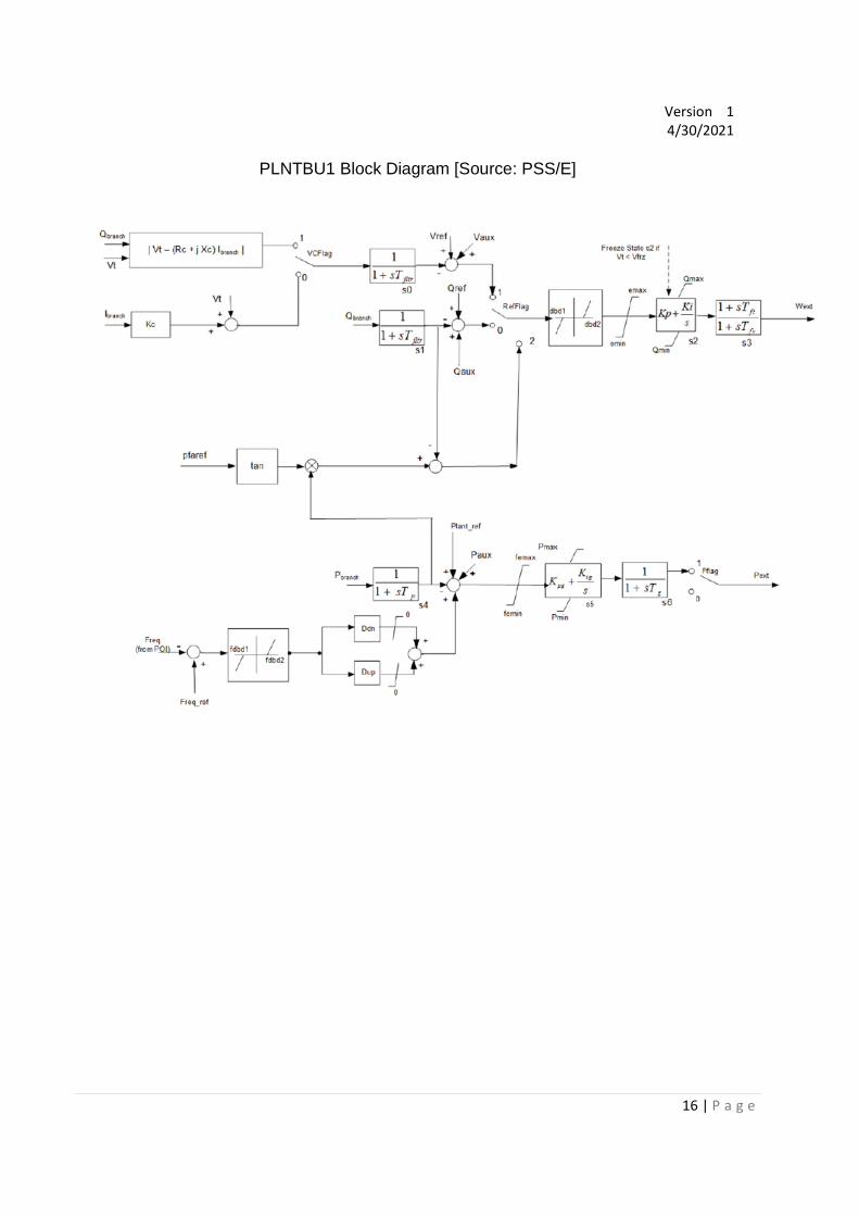
PLNTBU1 Block Diagram [Source: PSS/E]

Version 14/30/2021
17 | P a g e
REAX4BU1 Block Diagram [Source: PSS/E]