Gsm Temp Senser
60
Page 1 MAJOR PROJECT REPORT on GSM Based Remote Patient Monitoring System Submitted to DEPARTMENT OF ELECTRONICS AND COMMUNICATION IN PARTIAL FULFILLMENT FOR THE REQUIREMENT OF THE AWARD OF DEGREE OF BACHELOR OF TECHNOLOGY in ELECTRONICS AND COMMUNICATION SYSTEM Affiliated to MAHARISHI DAYANAND UNIVERSITY, ROHTAK (A State University established Under Haryana Act No. XXV of 1975) B++ Accredited University by NAAC Under the Guidance of: Submitted by: Mr. OP Thakur Tavleen Singh (08-ECE-219) (Project Guide) Vikramjeet (08-ECE-226) HOD, ECE Department Vinay Chahal (08-ECE-227) GITM, Gurgaon Virender Kaswan (08-ECE-228) GURGAON INSTITUTE OF TECHNOLOGY AND MANAGEMENT, GURGAON February-June 2012
-
Upload
vikram-sehdev -
Category
Documents
-
view
125 -
download
0
Transcript of Gsm Temp Senser

Page 1
MAJOR PROJECT REPORT
on
GSM Based Remote Patient Monitoring System
Submitted to
DEPARTMENT OF ELECTRONICS AND COMMUNICATION
IN PARTIAL FULFILLMENT FOR THE REQUIREMENT OF THE AWARD OF DEGREE
OF BACHELOR OF TECHNOLOGY
in
ELECTRONICS AND COMMUNICATION SYSTEM
Affiliated to
MAHARISHI DAYANAND UNIVERSITY, ROHTAK
(A State University established Under Haryana Act No. XXV of 1975)
B++ Accredited University by NAAC
Under the Guidance of: Submitted by:
Mr. OP Thakur Tavleen Singh (08-ECE-219)
(Project Guide) Vikramjeet (08-ECE-226)
HOD, ECE Department Vinay Chahal (08-ECE-227)
GITM, Gurgaon Virender Kaswan (08-ECE-228)
GURGAON INSTITUTE OF TECHNOLOGY AND MANAGEMENT, GURGAON
February-June 2012

Project REPORT
GURGAON INSTITUTE OF TECHNOLOGY AND MANAGEMENT
Bilaspur -Tauru Road, Gurgaon Haryana-122413
Ph. +91 – 124-2279501-03, Fax: +91-124-2279500
(Approved by AICTE, Govt. of Haryana & affiliated to MDU, ROHTAK)
Website: www.gitm.co.in
Dated: 11-05-2012
DECLARATION
We hereby certify that the major project entitled “ GSM Based Remote Patient Monitoring
System” Submitted by Ms. Tavleen singh (08-ECE-219), Mr. Vikramjeet (08-ECE-226),
Mr. Vinay Chahal (08-ECE-227) , Mr. Virender Kaswan (08-ECE-228) in partial
fulfilment of requirement for the award of degree of Bachelor of Technology in Electronics
and Communication submitted in the Department of Electronics and Communication at
GURGAON INSTITUTE OF TECHONOLOGY AND MANAGEMENT, GURGAON
affiliated to MAHARSHI DAYANAND UNIVERSITY, ROHTAK is an authentic record
of our own work carried out under the supervision of Mr. OP Thakur, Lecturer (ECE
Department) GITM. The matter presented has not been submitted by me in any other
University / Institute for the award of B.Tech Degree.
Ms. Tavleen Singh Mr. Vinay Chahal
( 1130125930) ( 1130125936)
Mr Vikramjeet Mr. Virender Kaswan
(1130125935) (1130125937)
This is to certify that the above statement made by the candidate is correct to the best of my
knowledge
Mr. OP Thakur Mr. Bijender M’dia
(Project Guide) (Project Coordinator)
HOD, ECE Department

Project REPORT
Acknowledgement
It gives us great pleasure and satisfaction to present major project report
entitled “GSM Based Remote Patient Monitoring System”. The completion of any
task is not only the reward to the person actively involved in accomplishing it,
but also the person involved in inspiring and guiding. I am highly indebted to
my supervisor Mr. Bijender M’dia for his invaluable support and guidance
throughout the work.
I extended my heartful thanks to Mr. Kamal Thakur, Director Gurgaon
Institute of Technology and Management (GITM), Gurgaon for providing
this opportunity to carry out major project.
I extended my heartful thanks to Prof. OP Thakur, HOD, Electronics and
Telecommunication for his support without which the work would have never
been realized. Last but not the least I would like to thank all friends who
directly or indirectly helped us in completion of work.
Ms. Tavleen Singh
Mr. Vikramjeet
Mr. Vinay Chahal
Mr. Virender Kaswan

Project REPORT
ABSTRACT
Wireless communication has announced its arrival on big stage and the world is going
mobile. We want to control everything and without moving an inch. This remote control of
appliances is possible through Embedded Systems. The use of “Embedded System in
Communication” has given rise to many interesting applications that ensures and safety to
human life.
The main aim of the project will be to design a SMS based health monitoring system toolkit.
It is proposed to design receive cum display toolkit which can be programmed from an
authorized mobile phone. The message to be is sent through a SMS from an authorized
transmitter (GSM modem).
This project aims at checking the health of the patient automatically and repeatedly. The
patients temperature is measured again and again and if the temperature exceeds the threshold
temperature entered then the message is send to the doctors mobile immediately and he can
attend the patient without any delay. The nurses in the hospital do not need to attend the
patient again and again, not only temperature but other devices like pressure sensor for blood
pressure monitoring can be also be added in this kit which serves the purpose of a complete
health monitoring toolkit.
This toolkit consists of a 8051 microcontroller which receives the temperature from the
temperature sensor and displays it on the LCD and if the temp. Exceeds the threshold it sends
it to the mobile of the doctor. Several temperature sensors can be interfaced to a single GSM
modem and monitoring the health of each patient in a routine way.
The system required for the purpose is nothing but a Microcontroller based SMS box. The
main components of the toolkit include microcontroller, GSM modem. These components are
integrated with the temp sensor and thus incorporate the wireless features.
The GSM modem receives the SMS. The AT commands are serially transferred to the
modem through MAX232. In return the modem transmits the stored message through the
COM port. The microcontroller validates the SMS and then displays the in the LCD display
board. Various time division multiplexing techniques have been suggested to make the
display boards functionally efficient. The microcontroller used in this case Atmel
AT89C51.SIM 300 is used as the GSM modem. In the prototype model, LCD display is used
for checking purpose. The results presented in the thesis support the proper functionalities
and working of the system. The timing diagram suggests the response of the modem to

Project REPORT
various AT commands. This project is to propose to be implemented in hospitals on large
scale and will prove to be useful to monitor the health of all patients of a ward.
LIST OF FIGURES:-
Fig. 2.1 Basic Design Overview
Fig. 3.1 SIM 300 GSM modem
Fig. 3.2 The screenshot of MS HyperTerminal's Connection Description
Fig.3.3 The screenshot of MS HyperTerminal's Connect
Fig. 3.4 The screenshot of MS HyperTerminal's Properties dialog box
Fig.3.5 The screenshot of MS HyperTerminal's main window in Windows 98.
Fig. 3.6 Pin Diagram of 8051
Fig 3.7 Block Diagram of 8051
Fig 3.8 Liquid Crystal Display
Fig 3.9 LCD Display
Fig 3.10 LCD Connection
Fig 3.11 LCD Interfacing with 8051
Fig 3.12 Rotary Temperature Potentiometer
Fig 3.13 IC 7805
Fig 3.14 LM35 Temperature Sensor
Fig 3.15 ADC 0804 Pin Diagram Fig 3.16 ADC interface with microcontroller
Fig 3.16 ADC interface with microcontroller
Fig 3.17 Resistors
Fig 3.18 Different types of Capacitors
Fig 3.19 Different types of Resistors
Fig 4.1 Keil Compiler.
Fig 4.2 Design on Proteus Software
Fig 4.3 Atmel AT89C2051 Device Programmer
Fig 4.4 Operational Flowchart
Fig 5.1 Transmission of AT Command from Microcontroller
Fig 5.2:- Reception of Response from MODEM
Fig 5.3 Tx and Rx Lines with ECHO being ON
Fig 5.4 Response of the Modem with the New Message

Project REPORT
LIST OF TABLES:-
Table 1:- SMS Related AT Commands
Table 2:- Port 1 Pins Description
Table 3:- Port 3 Pins Description
Table 4:- IC 7805 Pin Description
Table 5:- ADC 0804 Pin Description

Project REPORT
Contents 1. Introduction
1.1 Information 1.1.1 Information transfer
1.1.2 Broadcast 1.2 Project Objective 2. Design Overview
2.1 Design On Paper 3. Hardware Profile
3.1 Hardware Used 3.2 GSM Modem
3.2.1 Accessing GSM MODEM using Microsoft HyperTerminal 3.2.2 Testing GSM Modem 3.2.3 List Of Important AT Commands 3.2.4 Applications 3.3 Microcontroller 3.3.1 Features 3.3.2 Pin Diagram 3.3.3 Pin Description 3.3.4 Block Diagram 3.4 Liquid Crystal Display 3.5 Rotary Temperature Sensor
3.6 Power Supply 3.6.1 Voltage Regulator
3.7 Sensors 3.8 Analog To Digital ConvertorError! Bookmark not defined.
3.8.1 Pin Diagram 3.8.2 Pin Description 3.8.3 ADC Interface with Microcontroller 3.9 Resistors 3.10 Capacitors 4. Software Profile
4.1 Keil 8051 Development Tool 4.2 Proteus 38 4.3 Proload 38 4.4 Software Solvency 4.5 Control Flow In Code 4.5.1 Initializations 4.5.2 Display
4.5.3 Serial Transfer Using TI and RI Flags 5. Testing Methodologies And Observations
5.1 Offline Testing 5.2 Online Testing & Observations
6. Conclusion 6.1 Conclusion 6.2 Future Improvement
APPENDIX 1 APPENDIX 2

Project REPORT
CHAPTER 1
Introduction

Project REPORT
1. Introduction
Presently, the United States is the most technologically advanced country in the area of
telecommunications with about; 126 million phone lines, 7.5 million cellular phone users, 5
thousand AM radio broadcast stations, 5 thousand FM radio stations, 1 thousand television
broadcast stations, 9 thousand cable television systems, 530 million radios, 193 million
television sets, 24 ocean cables, and scores of satellite facilities! This is truly an "Information
Age" and sometimes, you need to look at where we've been in order to see the future more
clearly!
1.1 Information
“A message received and understood” --- Princeton
“Information is a term with many meanings depending on context, but is as a rule
closely related to such concepts as meaning, knowledge, instruction,
communication, representation, and mental stimulus ” --- Wikipedia
“Any communication or representation of knowledge such as facts, data, or
opinions in any medium or form, including textual, numerical, graphic, cartographic,
narrative, or audiovisual forms (OMB Circular A-130). ” --- Gils.net
“Facts, concepts, or instructions; any sort of knowledge or supposition which can be
communicated. “ --- cedar.web.cern
“Is organized data that has been arranged for better comprehension or
understanding. What is one person's information can become another person's
data.” --- earthlink.net
1.1.1 Information Transfer
A coordinated sequence of user and telecommunications system actions that cause
information present at a source user to become present at a destination user. Note: An
information-transfer transaction usually consists of three consecutive phases called the access
phase, the information-transfer phase, and the disengagement phase.
1.1.2 Broadcast
A term to describe communication where a piece of information is sent or transmitted from
one point to all other points. There is just one sender, but the information is simultaneously
sent to all connected receivers. In networking, a distinction is made between broadcasting
and multicasting. Broadcasting sends a message to everyone on the network whereas

Project REPORT
multicasting sends a message to a select list of recipients. One of the most common examples
is broadcast through a cellular network service. This serves multiple end users at different
locations in a simulcast fashion. Practically every cellular system has some kind of broadcast
mechanism. This can be used directly for distributing information to multiple mobiles,
commonly, for example in a mobile telephony system, the most important use of broadcast
information is to set up channels for one to one communication between the mobile Trans-
receiver and the base station. This is called paging. The details of the process of paging vary
somewhat from network to network, but normally we know a limited number of cells where
the phone is located (this group of cells is called a location area in the GSM system or
Routing Area in UMTS). Paging takes place by sending the broadcast message on all of those
cells. Today, interaction with digital displays is a deskbound or device-dependent experience.
1.2 PROJECT OBJECTIVE
OBJECTIVE: The main objective of this system is to develop a low cost system to monitor
the temperature of the Patient at some remote location and send the temperature readings to
the doctor at another location. GSM based temperature monitoring system is a portable and a
best replacement for the old model temperature. By this system doctors can know the
temperature of their emergency ward patients regularly even when they are not in the hospital
and in case of emergency he can take care of him. It is a combination of a temperature sensor
and microcontroller interfaced with a GSM module to transmit the temperature of the patient
to a remote location. This Project “GSM BASED REMOTE PATIENT MONITORING
SYSTEM” using Microcontroller is a reliable circuit .The primary function of this system is
to monitor the temperature of the Patient collected by the sensors. The readings are sent to the
Microcontroller in digital format and displayed on the LCD (Liquid Crystal Display)which is
interfaced to the microcontroller. The Microcontroller transmits the data over the air. Here we
are using the GSM modem in order to transmit the information. From the transmitter the
recordings are sent as an SMS to the mobile of the care taker or the expert which have been
given as the recipient in the GSM .Even the patient can use the temperature sensor to see
his/her temperature on the LCD display and can be even set up in the home of the patients.

Project REPORT
CHAPTER 2
Design Overview

Project REPORT
2. Design Overview
2.1 Design on Paper
The aim of this project is to design, build and test a “GSM BASED REMOTE PATIENT
MONITORING SYSTEM” circuit that can be used to monitor the health of the patients
regularly. The primary function of this system is to monitor the temperature of the Patient
continuously. The Microcontroller transmits the data to the GSM modem if the temperature
exceeds the normal temperature which alerts the doctor.
As explained in the introduction chapter, the realization of complete potential of the display
boards and the wireless medium in information transfer is the major issue that the following
thesis of the following project deals with.
Fig 2.1:- Basic Design Overview

Project REPORT
The “GSM BASED REMOTE MONITORING SYSTEM” circuit comprises of a 8051
microcontroller, SIM 300 GSM modem, temperature sensor, a ADC converter and an LCD
display. The 8051 microcontroller is the heart of the circuit. The AT89C51 is a low-power,
high-performance CMOS 8-bit microcomputer with 4k bytes of Flash programmable and
erasable read only memory (PEROM). The device is manufactured using Atmel’s high-
density non-volatile memory technology and is compatible with the industry-standard MCS-
51 instruction set and pin out .The temperatures sensor (LM-35) is touched with the finger tip
of the patient, which gives the analog temperature proportional to the physical temperature.
The output of LM-35 IC is provided to the ADC converter Ic-0804 which converts the analog
temperature into the digital temperature. This ADC is then interfaced to the microcontroller.
similarly the GSM modem and the LCD are interfaced to the microcontroller. The code in
8051 in written in such a way that the readings from the ADC converter are taken regularly
and the temperature is continuously displayed on the LCD and if the temperature exceeds the
temp fixed by the doctor the message is sent to the GSM modem which in turn sends it to the
mobile of the doctor.
This model can be set up in hospitals where a single GSM modem can be connected to three
or four patients in the same ward and any high temperature reading can alert the nurse to call
for immediate attention. This model not only makes its use in the temperature sensing only
but it can be used altogether for the collective data like pulse rate for monitoring the blood
pressure. There are numerous applications of GSM based microcontroller models.GSM
(Global System for Mobile Communications) is a low-cost hardware equipment to create a
system for remote monitoring and remote control. The system can be controlled and
monitored via Short Message Service (SMS) from anywhere that covered by GSM (Global
System for Mobile Communica- -tion) service. Devices that connect remote monitoring and
controlling of fans, TV sound, tube light, climate, door opening, closing and window’s and
multimedia entertainment systems. We can even control the appliances by sitting in our
homes, like if we forget to switch off our Ac’s we can turn them off with the help of a simple
message we send with our mobile. A most recent example of this is that we can even turn on
the Ac’s in our homes before we reach homes.

Project REPORT
Another example of this are the GSM based display boards in which we can display the
message on the LCD or Led based notice board Simple by sending the message from our
mobile phone to the GSM modem. This is even finding the applications in colleges and
schools.

Project REPORT
CHAPTER 3
Hardware Profile
Project REPORT
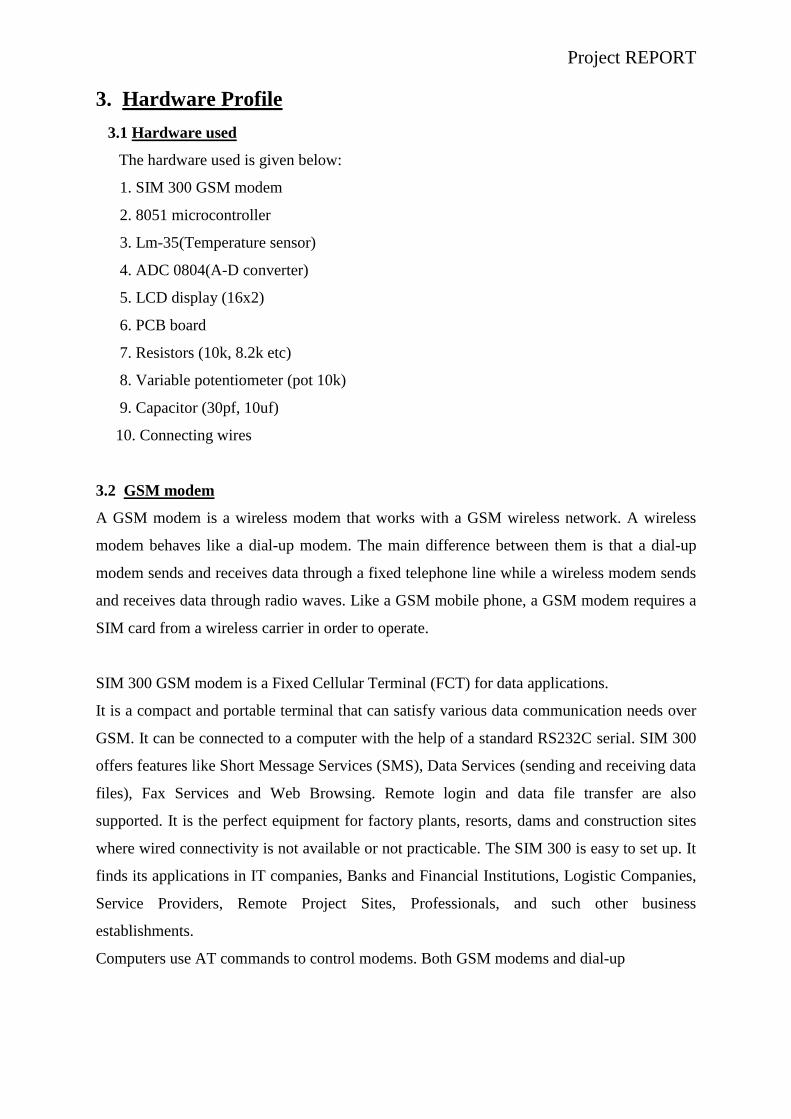
3. Hardware Profile
3.1 Hardware used
The hardware used is given below:
1. SIM 300 GSM modem
2. 8051 microcontroller
3. Lm-35(Temperature sensor)
4. ADC 0804(A-D converter)
5. LCD display (16x2)
6. PCB board
7. Resistors (10k, 8.2k etc)
8. Variable potentiometer (pot 10k)
9. Capacitor (30pf, 10uf)
10. Connecting wires
3.2 GSM modem
A GSM modem is a wireless modem that works with a GSM wireless network. A wireless
modem behaves like a dial-up modem. The main difference between them is that a dial-up
modem sends and receives data through a fixed telephone line while a wireless modem sends
and receives data through radio waves. Like a GSM mobile phone, a GSM modem requires a
SIM card from a wireless carrier in order to operate.
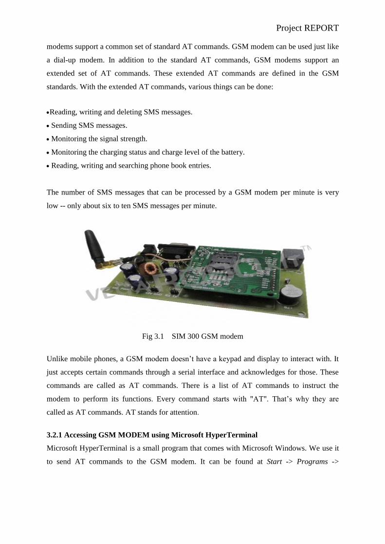
SIM 300 GSM modem is a Fixed Cellular Terminal (FCT) for data applications.
It is a compact and portable terminal that can satisfy various data communication needs over
GSM. It can be connected to a computer with the help of a standard RS232C serial. SIM 300
offers features like Short Message Services (SMS), Data Services (sending and receiving data
files), Fax Services and Web Browsing. Remote login and data file transfer are also
supported. It is the perfect equipment for factory plants, resorts, dams and construction sites
where wired connectivity is not available or not practicable. The SIM 300 is easy to set up. It
finds its applications in IT companies, Banks and Financial Institutions, Logistic Companies,
Service Providers, Remote Project Sites, Professionals, and such other business
establishments.
Computers use AT commands to control modems. Both GSM modems and dial-up
Project REPORT
modems support a common set of standard AT commands. GSM modem can be used just like
a dial-up modem. In addition to the standard AT commands, GSM modems support an
extended set of AT commands. These extended AT commands are defined in the GSM
standards. With the extended AT commands, various things can be done:
Reading, writing and deleting SMS messages.
Sending SMS messages.
Monitoring the signal strength.
Monitoring the charging status and charge level of the battery.
Reading, writing and searching phone book entries.
The number of SMS messages that can be processed by a GSM modem per minute is very
low -- only about six to ten SMS messages per minute.
Fig 3.1 SIM 300 GSM modem
Unlike mobile phones, a GSM modem doesn’t have a keypad and display to interact with. It
just accepts certain commands through a serial interface and acknowledges for those. These
commands are called as AT commands. There is a list of AT commands to instruct the
modem to perform its functions. Every command starts with "AT". That’s why they are
called as AT commands. AT stands for attention.
3.2.1 Accessing GSM MODEM using Microsoft HyperTerminal
Microsoft HyperTerminal is a small program that comes with Microsoft Windows. We use it
to send AT commands to the GSM modem. It can be found at Start -> Programs ->

Project REPORT
Accessories -> Communications -> HyperTerminal. Before
programming our SMS application, it is required to check if the GSM modem and SIM card
are working properly first. The MS HyperTerminal is a handy tool when it comes to testing
the GSM device. It is a good idea to test the GSM devices beforehand. When a problem
occurs, sometimes it is difficult to tell what causes the problem. The cause can be the
program, the GSM device or the SIM card. If GSM device and SIM card with MS
HyperTerminal and they operate properly, then it is very likely that the problem is caused by
the program or other hard wares.
For Linux users, Mincom can be used instead of HyperTerminal.
3.2.2 Testing of GSM MODEM
To use MS HyperTerminal to send AT commands to the GSM modem, the following
procedure is followed:
1. We put a valid SIM card into the GSM modem. We can obtain a SIM card by subscribing
to the GSM service of a wireless network operator.
2. Since in our case the modem drivers were pre installed, we need not to install any such
drivers.
3. Then we start up MS HyperTerminal by selecting Start -> Programs ->
Accessories -> Communications -> HyperTerminal.
4. In the Connection Description dialog box (as shown in the screenshot given below) we
enter any name and choose an icon we like for the connection. Then we click the OK button.
Fig 3.2. The screenshot of MS HyperTerminal's Connection Description
5. In the Connect To dialog box, choose the COM port that your mobile phone or

Project REPORT
GSM modem is connecting to in the Connect using combo box. For example, choose COM1
if your mobile phone or GSM modem is connecting to the COM1 port. Then click the OK
button.(Sometimes there will have more than one COM port in the Connect using combo box.
To know which COM port is used by your mobile phone or GSM modem, follow the
procedure below.
In Windows 98:
Go to Control Panel -> Modem. Then click the Diagnostics tab. In the list box, you can see
which COM port the mobile phone or GSM modem is connected to.
In Windows 2000 and Windows XP:
Go to Control Panel -> Phone and Modem Options. Then click the Modems tab. In the list
box, you can see which COM port the mobile phone or GSM modem is connected to dialog
box
Figure.3.3 The screenshot of MS HyperTerminal's Connect
6. The Properties dialog box comes out. Enter the correct port settings for your mobile phone
or GSM modem. Then click the OK button.
(To find the correct port settings that should be used with your mobile phone or
GSM modem, one way is to consult the manual of your mobile phone or GSM modem.
Another way is to check the port settings used by the wireless modem driver that you
installed earlier.

Project REPORT
To check the port settings used by the wireless modem driver on Windows 98, follow these
steps:
a. Go to Control Panel -> Modem.
b. Select your mobile phone or GSM modem in the list box.
c. Click the Properties button.
d. The Properties dialog box appears. The Maximum speeds field on the General tab
corresponds to HyperTerminal's Bits per second field. Click the Connection tab and you can
find the settings for data bits, parity and stop bits. Click the
Advanced button and you can find the setting for flow control.
To check the port settings used by the wireless modem driver on Windows 2000 and
Windows XP, follow these steps:
a. Go to Control Panel -> Phone and Modem Options -> Modems tab.
b. Select your mobile phone or GSM modem in the list box.
c. Click the Properties button.
d. The Properties dialog box appears. Click the Advanced tab and then click the Change
Default Preferences button.
e. The Change Default Preferences dialog box appears. The Port speed field on the General
tab corresponds to HyperTerminal's Bits per second field. You can also find the setting for
flow control on the General tab. On the Advanced tab, you can find the settings for data bits,
parity and stop bits.)

Project REPORT
Figure 3.4 The screenshot of MS HyperTerminal's Properties dialog box
7. Type "AT" in the main window. A response "OK" should be returned from the mobile
phone or GSM modem. Type "AT+CPIN?" in the main window. The AT command
"AT+CPIN?" is used to query whether the mobile phone or GSM modem is waiting for a PIN
(personal identification number, i.e. password). If the response is "+CPIN: READY", it
means the SIM card does not require a PIN and it is ready for use. If your SIM card requires a
PIN, you need to set the PIN with the AT command "AT+CPIN=<PIN>".
Figure.3.5 The screenshot of MS HyperTerminal's main window in Windows 98.

Project REPORT
If you get the responses above, your mobile phone or GSM modem is working properly. You
can start typing your own AT commands to control the mobile phone or GSM modem.
3.2.3 List of Important AT Commands
After successfully testing the MODEM for its correct operational state, we need to set the
MODEM parameters like Baud rate, Echo off etc to enable easier access via a
microcontroller which we used in this project. Following is a list of the important AT
commands
Example: Changing and saving parameters
AT+IPR=2400[Enter] Transfer rate to 2400 bps
AT&W[Enter] save parameters
Send and Receive
Example: Data transfer
AT+CPIN="xxxx"[Enter] enters PIN
15
AT+CREG?[Enter] Register Network (0,1 means logged in)
ATD05111234567 [Enter] Data call
Example: Send SMS with GSM modem / module
Enter SMS-Centre
AT+CSCA=+491722270000[Enter] Enter SMS-Centre for Vodafone Germany (T-Mobile
Germany = +491710760000)
Example: Send SMS
AT+CMGF=1[Enter]
AT+CMGS="+491711234567"[Enter]
>Please call office^Z
+CMGF=1 - set modem in text mode
Send SMS (^Z equals StrgZ). At D2 you can
send without international and local code. If you
dial with Int. and local code the transmission
from foreign networks are ensured.
Example: Receive SMS
A SMS will be stored in the GSM modem / module and being sent via RS232 to the

Project REPORT
peripherals. The peripherals have to send commands to the GSM unit to receive SMS and to
erase SMS from the device in order to free memory.
+CMTI:"SM",x X stands for the memory number of received SMS
AT+CMGR=X [Enter] Read SMS on memory number X
AT+CMGD=X [Enter] Erase SMS on memory number X
ATZ; E [Enter] Echo OFF
ATZ;E1 [Enter] Echo ON
AT+ COPS? [Enter] Shows if network of SIM-card is available. 0,2,26201= D1 available
AT+COPS=? [Enter] Shows all available networks.
Table 1:- SMS Related AT Commands
SMS Related AT Commands
AT It is used to test the connection.
AT+CMGF=1 It is used to instruct the modem to operate in text mode.
AT+CMGF=0 will instruct the modem to operate in PDU mode.
AT+CMGS="mobile
number"
It is used to send a text message. It accepts the recipient mobile
number. As soon as this command is accepted the modem waits for
the message content. The text message has to be sent sequentially
and terminated by the char 0x1A.
AT+CMGW="mobile
number"
It is used to store a message in the memory. After execution it
returns an index for the message stored. E.g.: AT+CMGW=1. Here
1 is the index for the saved message. Later this index is used to
process the message like deleting it or forwarding to the recipient
number.
AT+CMGD=2
It is used to delete a message from the storage. The index of the
stored message is used to delete it. Above command deletes the
message with index 2.

Project REPORT
In our Simple project, the program waits for the mobile number to be entered through the
keyboard. When a ten digit mobile number is provided, the program instructs the modem to
send the text message using a sequence of AT commands.
Steps to check your GSM modem:
The GSM modem can be tested by connecting it with a PC. The modem is equipped
with a RS232 cable. Just use a Serial to USB converter and connect it with the PC.
Now you can proceed with sending the commands to the modem using any serial
communication program like HyperTerminal, minicom etc. Ensure the serial
parameters are configured to 8N1 and the baud rate is set to 9600bps.
For each command you send the modem acknowledges with a message. Example:
Just try sending "AT" to the modem. It sends back a result code "OK" which states
that the modem is responding. If it’s not working fine, it sends "ERROR".
3.2.4 Applications
1. All the parameters can be viewed on the mobile phone.
2. Most reliable.
3. Cost effective.
4. Supports innumerable sensors to the system.
3.3 Microcontroller
The AT89C51 is a low-power, high-performance CMOS 8-bit microcomputer with 4K bytes
of Flash programmable and erasable read only memory (PEROM). The device is
manufactured using Atmel’s high-density non-volatile memory technology and is compatible
with the industry-standard MCS-51 instruction set and pin out. The on-chip Flash allows the
program memory to be reprogrammed in-system or by a conventional non-volatile memory
programmer. By combining a versatile 8-bit CPU with Flash on a monolithic chip, the Atmel
AT89C51 is a powerful microcomputer which provides a highly-flexible and cost-effective
solution to many embedded control applications. The AT89C51 is a low-power, high-

Project REPORT
performance CMOS 8-bit microcomputer with 4K bytes of Flash programmable and erasable
read only memory (PEROM). The device is manufactured using Atmel’s high-density non-
volatile memory technology and is compatible with the industry-standard MCS-51 instruction
set and pin out. The on-chip Flash allows the program memory to be reprogrammed in-
system or by a conventional non-volatile memory programmer. By combining a versatile 8-
bit CPU with Flash a monolithic chip, the Atmel AT89C51 is a powerful microcomputer
which provides a highly-flexible and cost-effective solution to many embedded control
applications.
3.3.1 FEATURES
8K Bytes of In-System Reprogrammable Flash Memory
Fully Static Operation: 0 Hz to 33 MHz
Three-level Program Memory Lock
256 x 8-bit Internal RAM
32 Programmable I/O Lines
Three 16-bit Timer/Counters
Eight Interrupt Sources
Programmable Serial Channel
Low-power Idle and Power-down Modes
4.0V to 5.5V Operating Range
Full Duplex UART Serial Channel
Interrupt Recovery from Power-down Mode
Watchdog Timer
Dual Data Pointer
Power-off Flag
Fast Programming Time

Project REPORT
3.3.2 PIN DIAGRAM:
Fig 3.6 Pin Diagram of 8051
3.3.3 PIN DESCRIPTION:
VCC
Supply voltage.
GND
Ground
Port 0
Port 0 is an 8-bit open drain bidirectional I/O port. As an output port, each pin can sink
eight TTL inputs. When 1s are written to port 0 pins, the pins can be used as high impedance
inputs. Port 0 can also be configured to be the multiplexed low order address/data bus during
accesses to external program and data memory. In this mode, P0 has internal pull-ups. Port 0
also receives the code bytes during Flash programming and outputs the code bytes during
program verification. External pull-ups are required during program verification.
Port 1
Port 1 is an 8-bit bidirectional I/O port with internal pull-ups. The Port 1 output
buffers can sink/source four TTL inputs. When 1s are written to Port 1 pins, they are pulled
high by the internal pull-ups and can be used as inputs. As inputs, Port 1 pins that are

Project REPORT
externally being pulled low will source current (IIL) because of the internal pull-ups. In
addition, P1.0 and P1.1 can be configured to be the timer/counter 2 external count input
(P1.0/T2) and the timer/counter 2 trigger input (P1.1/T2EX), respectively, as shown in the
following table. Port 1 also receives low order address bytes during Flash programming and
verification.
Table 2:- Port 1 Pins Description
Port 2
Port 2 is an 8-bit bidirectional I/O port with internal pull-ups. The Port 2 output buffers
can sink/source four TTL inputs. When 1s are written to Port 2 pins, they are pulled high by
the internal pull-ups and can be used as inputs. As inputs, Port 2 pins that are externally being
pulled low will source current (IIL) because of the internal pull-ups. Port 2 emits the high-
order address byte during fetches from external program memory and during accesses to
external data memory that uses 16-bit addresses (MOVX @ DPTR). In this application, Port
2 uses strong internal pull-ups when emitting 1s. During accesses to external data memory
that uses 8-bit addresses (MOVX @ RI), Port 2 emits the contents of the P2 Special Function
Register. Port 2 also receives the high-order address bits and some control signals during
Flash programming and verification.
Port 3
Port 3 is an 8-bit bidirectional I/O port with internal pull-ups. The Port 3 output
buffers can sink/source four TTL inputs. When 1s are written to Port 3 pins, they are pulled
high by the internal pull-ups and can be used as inputs. As inputs, Port 3 pins that are
externally being pulled low will source current (IIL) because of the pull-ups. Port 3 also

Project REPORT
serves the functions of various special features of the AT89S52, as shown in the following
table. Port 3 also receives some control signals for Flash programming and verification.
Table 3:- Port 3 Pins Description
RST
Reset input. A high on this pin for two machine cycles while the oscillator is running
resets the device. This pin drives High for 96 oscillator periods after the Watchdog times out.
The DISRTO bit in SFR AUXR (address 8EH) can be used to disable this feature. In the
default state of bit DISRTO, the RESET HIGH out feature is enabled. ALE/PROG Address
Latch Enable (ALE) is an output pulse for latching the low byte of the address during
accesses to external memory. This pin is also the program pulse input (PROG) during Flash
programming. In normal operation, ALE is emitted at a constant rate of 1/6 the oscillator
frequency and may be used for external timing or clocking purposes. Note, however, that one
ALE pulse is skipped during each access to external data memory. If desired, ALE operation
can be disabled by setting bit 0 of SFR location 8EH. With the bit set, ALE is active only
during a MOVX or MOVC instruction. Otherwise, the pin is weakly pulled high. Setting the
ALE-disable bit has no effect if the microcontroller is in external execution mode.
PSEN
Program Store Enable (PSEN) is the read strobe to external program memory. When
the AT89S52 is executing code from external program memory, PSEN is activated twice
each machine cycle, except that two PSEN activations are skipped during each access to
external data memory.

Project REPORT
EA/VPP
External Access Enable. EA must be strapped to GND in order to enable the device
to fetch code from external program memory locations starting at 0000H up to FFFFH. Note,
however, that if lock bit 1 is programmed, EA will be internally latched on reset. EA should
be strapped to VCC for internal program executions. This pin also receives the 12-volt
programming enable voltage
(VPP) during Flash programming.
XTAL1
Input to the inverting oscillator amplifier and input to the Internal clock operating
circuit.
XTAL2
Output from the inverting oscillator amplifier.

Project REPORT
3.3.4 Block Diagram
Fig 3.7 Block Diagram of 8051

Project REPORT
3.4 LIQUID CRYSTAL DISPLAY
LCD stands for Liquid Crystal Display. LCD is finding wide spread use replacing LEDs
(seven segment LEDs or other multi segment LEDs) because of the following reasons:
1. The declining prices of LCDs.
2. The ability to display numbers, characters and graphics. This is in contrast to LEDs,
which are limited to numbers and a few characters.
3. Incorporation of a refreshing controller into the LCD, thereby relieving the CPU of
the task of refreshing the LCD. In contrast, the LED must be refreshed by the CPU to
keep displaying the data.
4. Ease of programming for characters and graphics.
Fig 3.8 Liquid Crystal Display
LCD (Liquid Crystal Display) screen is an electronic display module and find a wide range of
applications. A 16x2 LCD display is very basic module and is very commonly used in
various devices and circuits. These modules are preferred over seven segments and other
multi segment LEDs. The reasons being: LCDs are economical; easily programmable; have
no limitation of displaying special & even custom characters (unlike in seven
segments), animations and so on.
A 16x2 LCD means it can display 16 characters per line and there are 2 such lines. In this
LCD each character is displayed in 5x7 pixel matrix. This LCD has two registers, namely,
Command and Data.

Project REPORT
The command register stores the command instructions given to the LCD. A command is an
instruction given to LCD to do a predefined task like initializing it, clearing its screen, setting
the cursor position, controlling display etc. The data register stores the data to be displayed
on the LCD. The data is the ASCII value of the character to be displayed on the LCD.
LCD SCREEN
LCD screen consists of two lines with 16 characters each. Each character consists of 5x7 dot
matrix. Contrast on display depends on the power supply voltage and whether messages are
displayed in one or two lines. For that reason, variable voltage 0-Vdd is applied on pin
marked as VEE. Trimmer potentiometer is usually used for that purpose. Some versions of
displays have built in backlight (blue or green diodes). When used during operating, a resistor
for current limitation should be used (like with any LE diode).
Fig 3.9 LCD Display

Project REPORT
LCD Connection
Fig 3.10 LCD Connection
Depending on how many lines are used for connection to the microcontroller, there are 8-bit
and 4-bit LCD modes. The appropriate mode is determined at the beginning of the process in
a phase called “initialization”. In the first case, the data are transferred through outputs D0-
D7 as it has been already explained. In case of 4-bit LED mode, for the sake of saving
valuable I/O pins of the microcontroller, there are only 4 higher bits (D4-D7) used for
communication, while other may be left unconnected.
Consequently, each data is sent to LCD in two steps: four higher bits are sent first (that
normally would be sent through lines D4-D7), four lower bits are sent afterwards. With the
help of initialization, LCD will correctly connect and interpret each data received.
Besides, with regards to the fact that data are rarely read from LCD (data mainly are
transferred from microcontroller to LCD) one more I/O pin may be saved by Simple
connecting R/W pin to the Ground. Such saving has its price.
Even though message displaying will be normally performed, it will not be possible to read
from busy flag since it is not possible to read from display.

Project REPORT
3.5 Rotary Temperature Potentiometer
Fig. 3.12 Rotary Temperature Potentiometer
A potentiometer, informally, a pot, in electronics technology is a component, a three-
terminal resistor with a sliding contact that forms an adjustable voltage divider. If only two
terminals are used, one end and the wiper, it acts as a variable resistor or rheostat.
Fig 3.11 LCD Interfacing with 8051

Project REPORT
In circuit theory and measurement a potentiometer is essentially a voltage divider used for
measuring electric potential (voltage); the component is an implementation of the same
principle, hence its name.
Potentiometers are commonly used to control electrical devices such as volume controls on
audio equipment. Potentiometers operated by a mechanism can be used as
position transducers, for example, in a joystick.
Potentiometers are rarely used to directly control significant power (more than a watt), since
the power dissipated in the potentiometer would be comparable to the power in the controlled
load (see infinite switch). Instead they are used to adjust the level of analog signals
(e.g. volume controls on audio equipment), and as control inputs for electronic circuits. For
example, a light dimmer uses a potentiometer to control the switching of a TRIAC and so
indirectly to control the brightness of lamps.
Potentiometers comprise a resistive element, a sliding contact (wiper) that moves along the
element, making good electrical contact with one part of it, electrical terminals at each end of
the element, a mechanism that moves the wiper from one end to the other, and a housing
containing the element and wiper.
The resistive element of inexpensive potentiometers is often made of graphite. Other
materials used include resistance wire, carbon particles in plastic, and a ceramic/metal
mixture called cermet. Conductive track potentiometers use conductive polymer resistor
pastes that contain hard-wearing resins and polymers, solvents, and lubricant, in addition to
the carbon that provides the conductive properties. The tracks are made by screen-printing the
paste onto a paper-based phenolic substrate and then curing it in an oven. The curing process
removes all solvents and allows the conductive polymer to polymerize and cross-link. This
produces a durable track with electrical resistance which is stable throughout its working life.
Low-resistance wire-wound potentiometers may be made with resistive wire close-wound
round a former with a slider jumping from turn to turn.
Here we have used rotator potentiometer which converts the rotatory action of the screw into
a reading.

Project REPORT
3.6 POWER SUPPLY
3.6.1 VOLTAGE REGULATOR
A Voltage regulator is a device which converts varying input voltage into a constant
regulated output voltage.
IC 7805:
Fig 3.13 IC 7805
IC 7805 is an integrated three-terminal positive fixed linear voltage regulator. It supports an
input voltage of 10 volts to 35 volts and output voltage of 5 volts. It has a current rating of 1
amp although lower current models are available. Its output voltage is fixed at 5.0V. The
7805 also has a built-in current limiter as a safety feature. 7805 is manufactured by many
companies, including National Semiconductors and Fairchild Semiconductors.
The 7805 will automatically reduce output current if it gets too hot. The last two digits
represent the voltage; for instance, the 7812 is a 12-volt regulator. The 78xx series of
regulators is designed to work in complement with the 79xx series of negative voltage
regulators in systems that provide both positive and negative regulated voltages, since the
78xx series can't regulate negative voltages in such a system.
The 7805 & 78 is one of the most common and well-known of the 78xx series regulators, as
it's small component count and medium-power regulated 5V make it useful for powering
TTL devices.
Pin No Function Name
1 Input voltage (5V-18V) Input
2 Ground (0V) Ground
3 Regulated output; 5V (4.8V-5.2V) Output
Table 4:- IC 7805 Pin Description

Project REPORT
3.7 SENSORS
The sensor used in this project is Temperature sensor (LM 35). The output of temperature
sensor is given to the ADC so as to convert the analog value into digital data and then give it
to the microcontroller.
LM35 is a precision IC temperature sensor with its output proportional to the temperature
(in oC). The sensor circuitry is sealed and therefore it is not subjected to oxidation and other
processes. With LM35, temperature can be measured more accurately than with a
thermistor. It also possess low self heating and does not cause more than 0.1 o
C temperature
rise in still air. The operating temperature range is from -55°C to 150°C. The output voltage
varies by 10mV in response to every oC rise/fall in ambient temperature, i.e., its scale factor
is 0.01V/ oC.
Fig 3.14 LM35 Temperature Sensor
FEATURES
Calibrated directly in ° Celsius (Centigrade)
Linear + 10.0 mV/°C scale factor
0.5°C accuracy guaranteed (at +25°C)
Rated for full −55° to +150°C range

Project REPORT
Suitable for remote applications
Low cost due to wafer-level trimming
Operates from 4 to 30 volts
Less than 60 μA current drain
Low self-heating, 0.08°C in still air
Nonlinearity only ±1⁄4°C typical
Low impedance output, 0.1 W for 1 mA load
For each degree of centigrade temperature it outputs 10 milli volts.
3.8 ANALOG TO DIGITAL CONVERTER
Analog-to-digital converters are among the most widely used devices for data
acquisition. Digital systems use binary values, but in the physical world everything is
continuous i.e., analog values. Temperature, pressure (wind or liquid), humidity and velocity
are the physical analog quantities. These physical quantities are to be converted into digital
values for further processing. One such device to convert these physical quantities into
electrical signals is sensor. Sensors for temperature, pressure, humidity, light and many other
natural quantities produce an output that is voltage or current.
3.8.1 PIN DIAGRAM
Fig 3.15 ADC 0804 Pin Diagram

Project REPORT
ADC0804: The ADC chip that is used in this project is ADC0804. The ADC0804 IC is an 8-
bit parallel ADC in the family of the ADC0800 series from National Semiconductor. It works
with +5 volts and has a resolution of 8 bits. In the ADC0804, the conversion time varies
depending on the clocking signals applied to the CLK IN pin, but it cannot be faster than
110µs.
3.8.2 PIN DESCRIPTION
Table 5:- ADC 0804 Pin Description
Pin
No
Function Name
1 Activates ADC; Active low Chip select
2 Input pin; High to low pulse brings the data from internal
registers to the output pins after conversion
Read
3 Input pin; Low to high pulse is given to start the conversion Write
4 Clock Input pin; to give external clock. Clock IN
5 Output pin; Goes low when conversion is complete Interrupt
6 Analog non-inverting input Vin(+)
7 Analog inverting Input; normally ground Vin(-)
8 Ground(0V) Analog Ground
9 Input pin; sets the reference voltage for analog input Vref/2
10 Ground(0V) Digital Ground
11
8 bit digital output pins
D7
12 D6
13 D5
14 D4
15 D3
16 D2
17 D1
18 D0
19 Used with Clock IN pin when internal clock source is used Clock R
20 Supply voltage; 5V Vcc

Project REPORT
3.8.3 ADC Interface with Microcontroller:
Fig 3.16 ADC interface with microcontroller
3.9 RESISTORS:
Resistance is the opposition of a material to the current. It is
conductors represent a certain amount of resistance, since no conductor is 100% efficient. To
control the electron flow (current) in a predictable manner, we use resistors. Electronic
circuits use calibrated lumped resistance to control the flow of current. Broadly speaking,
resistor can be divided into two groups viz. fixed & adjustable (variable) resistors. In fixed
resistors, the value is fixed & cannot be varied. In variable resistors, the resistance value can
be varied by an adjuster knob. It can be divided into (a) Carbon composition (b) Wire wound
(c) Special type. The most common type of resistors used in our projects is carbon type. The
resistance value is normally indicated by color bands. Each resistance has four colors, one of
the band on either side will be gold or silver, this is called fourth band and indicates the
tolerance, others three band will give the value of resistance (see table). For example if a
resistor has the following marking on it say red, violet, gold. Comparing these colored rings
with the color code, its value is 27000 ohms or 27 kilo ohms and its tolerance is ±5%.
Resistor comes in various sizes (Power rating). The bigger the size the more power rating of
1/4 watts. The four color rings on its body tells us the value of resistor value as given below.

Project REPORT
COLOURS CODE
Black ----------------------------------------------------- 0
Brown ---------------------------------------------------- 1
Red ------------------------------------------------------- 2
Orange --------------------------------------------------- 3
Yellow --------------------------------------------------- 4
Green ----------------------------------------------------- 5
Blue ------------------------------------------------------ 6
Violet ----------------------------------------------------- 7
Grey ------------------------------------------------------ 8
White ----------------------------------------------------- 9
Figure3.17:Resistors
The first rings give the first digit. The second ring gives the second digit. The third ring
indicates the number of zeroes to be placed after the digits. The fourth ring gives tolerance
(gold ±5%, silver ± 10%, No colour ± 20%).In variable resistors, we have the dial type of
resistance boxes. There is a knob with a metal pointer. This presses over brass pieces placed
along a circle with some space b/w each of them. Resistance coils of different values are
connected b/w the gaps. When the knob is rotated, the pointer also moves over the brass

Project REPORT
pieces. If a gap is skipped over, its resistance is included in the circuit. If two gaps are
skipped over, the resistances of both together are included in the circuit and so on.
A dial type of resistance box contains many dials depending upon the range, which it has to
cover. If a resistance box has to read upto 10,00Ω, it will have three dials each having ten
gaps i.e. ten resistance coils each of resistance 10Ω. The third dial will have ten resistances
each of 100Ω.The dial type of resistance boxes is better because the contact resistance in this
case is small & constant.
3.10 CAPACITORS:
A capacitor is a little like a battery. Although they work in completely different ways,
capacitors and batteries both store electrical energy. If you have read How Batteries Work,
then you know that a battery has two terminals. Inside the battery, chemical reactions produce
electrons on one terminal and absorb electrons at the other terminal.
Figure3.18 Different types of capacitors
Figure3.19 Different types of resistors

Project REPORT
CHAPTER 4
Software Profile

Project REPORT
4. Software profile
4.1 Keil 8051 Development Tool
The Keil 8051 Development Tools are designed to solve the complex problems
facing embedded software developers. The Keil µVision Debugger accurately simulates on-
chip peripherals (I²C, CAN, UART, SPI, Interrupts, I/O Ports, A/D Converter, D/A
Converter, and PWM Modules) of your 8051 device. Simulation helps you understand hard
ware configurations and avoids time wasted on setup problems. Additionally, with
simulation, you can write and test applications before target hardware is available. The code
is written in c language which is “embedded c programming” (given in appendix A).This
code is compiled in keil compiler .The keil compiler generates the hex code which is then
burned into the 8051 microcontroller.
The keil compiler is a very good software for checking our source code and it nearly works
on all vendor’s microcontrollers including microchip, Atmel and Texas instruments.
On next page is shown the picture of keil compiler which is compiling the source code.
Fig 4.1 Keil Compiler.

Project REPORT
4.2 Proteus 7(design software)
Proteus is software for microprocessor simulation, schematic capture, and printed circuit
board (PCB) design. It is developed by Electronics. We are using proteus only for the
purpose of circuit simulation and checking our circuit finally. Proteus provides the simulation
with the same components which we are using in our real circuit.
Fig 4.2 Design on Proteus Software
4.3 Proload:
Proload is software which accepts only hex files. Once the machine code is converted into
hex code, that hex code has to be dumped into the microcontroller and this is done by the
Proload. Proload is a programmer which itself contains a microcontroller in it other than the
one which is to be programmed. This microcontroller has a program in it written in such a
way that it accepts the hex file from the Keil compiler and dumps this hex file into the
microcontroller which is to be programmed. As the Proload programmer kit requires power

Project REPORT
supply to be operated, this power supply is given from the power supply circuit designed
above. It should be noted that this programmer kit contains a power supply section in the
board itself but in order to switch on that power supply, a source is required. Thus this is
accomplished from the power supply board with an output of 12volts.
Fig 4.3 Atmel AT89C2051 Device Programmer
Features
Supports major Atmel 89 series devices
Auto Identify connected hardware and devices
Error checking and verification in-built
Lock of programs in chip supported to prevent program copying
20 and 40 pin ZIF socket on-board
Auto Erase before writing and Auto Verify after writing
Informative status bar and access to latest programmed file
Simple and Easy to use
Works on 57600 speed

Project REPORT
4.4 Software Solvency:
NO
NO
Fig. 4.4 Operational Flowchart
LCD
If temp>30
YE
S
Message is
sent to
mobile
YES
Start
Read the
temperature
Initialize
baud rate
Serial transmission
AT+CMGF=1
“OK”
received
from GSM
modem?

Project REPORT
4.5 Control Flow in Code
4.5.1. Initializations
The baud rate of the modem was set to be 9600 bps using the HyperTerminal .The ECHO
from the modem was turned off using the command ATE/ATE0 at the hyper terminal. For
serial transmission and reception to be possible both the DTE and DCE should have same
operational baud rates. Hence to set the microcontroller at a baud rate of 9600 bps, we set
terminal count of Timer 1 at 0FDh (clock frequency = 1.8432). The TCON and SCON
registers were set accordingly..
4.5.2 Display
The ADC converts readings from the temperature sensor and provide it to the
microcontroller. The microcontroller sends the readings to the LCD display and thereafter
compares the readings with the threshold provided by us. If the threshold exceeds the
temperature then a message goes to the doctor’s mobile number saved in the computer.
4.5.3 Serial transfer using TI and RI flags
After setting the baud rates of the two devices both the devices are now ready to transmit and
receive data in form of characters. Transmission is done when TI flag is set and similarly data
is known to be received when the Rx flag is set. The microcontroller then sends an AT
command to the modem in form of string of characters serially just when the TI flag is set.
After reception of a character in the SBUF register of the microcontroller (response of
MODEM with the read message in its default format or ERROR message or OK message),
the RI flag is set and the message is sent to the GSM modem from the microcontroller.

Project REPORT
CHAPTER 5
TESTING METHODOLOGIES AND
OBSERVATIONS

Project REPORT
5. TESTING METHODOLOGIES AND OBSERVATIONS
5.1 Offline Testing
Figure 5.1 Transmission of AT Command from Microcontroller
Figure 5.2:- Reception of Response from MODEM
Offline testing refers to the initial phase of testing where the module is not yet connected to
the wireless medium. This is the part of the testing process wherein we check if the MODEM
receives the AT commands from the microcontroller and makes its response in form of a new
message, an ERROR message, or an OK message (all in form of bit strings. The oscilloscope
probes are connected to P3.0 & P3.1 which are internally connected to the Tx and Rx lines of
the microcontroller. Online testing requires proper timing and delay routines, and of course
the validations step to be included.
5.2. Online Testing & Observations
After inclusion of the validation module in the program code, we test the module in
online mode. In this prototype we used only one valid number. With more memory
available three or four valid numbers can be included. When a message is sent to number
carried by the SIM of the MODEM, the validation module of the program checks character
by character the sender’s number with the number stored in the memory as the valid or

Project REPORT
authentic number (in our case the only valid number).With the same probe connections as in
the case of offline testing, we then look for signals on the Tx and Rx lines. What we see
below on the left are the signals on these lines with the ECHO being ON(ATE1). The
corresponding picture on the right depicts the modem response after about 460 ms (variable
as per message length :D) delay with the new message.
Figure 5.3 Tx and Rx Lines with Figure5.4 Response of the Modem with
ECHO being ON. the New Message

Project REPORT
CHAPTER 6
CONCLUSION

Project REPORT
6. CONCLUSION
6.1 Conclusion
The implementation of Temperature Monitoring System using GSM is done successfully.
The communication is properly done without any interference between different modules in
the design. Design is done to meet all the specifications and requirements. Software tools like
Keil Uvision Simulator, Proload to dump the source code into the microcontroller, Orcad Lite
for the schematic diagram have been used to develop the software code before realizing the
hardware.
The performance of the system is more efficient. Continuously reading the output
from the sensors and pass the data to the doctor’s mobile whenever the read values exceed the
normal values or whenever the doctor sends a request to the controlling unit is the main job
carried out by the microcontroller. The mechanism is controlled by the microcontroller.
Circuit is implemented in Orcad and implemented on the microcontroller board. The
performance has been verified both in software Simulator and hardware design. The total
circuit is completely verified functionally and is following the application software. It can be
concluded that the design implemented in the present work provide portability, flexibility and
the data transmission is also done with low power consumption.
6.2 Future Improvement
The project aims to be implemented in the hospitals very soon. Other sensors can also be
attached to it so it can be made a complete health monitoring toolkit. This project can be
implemented vice-versa, one such implementation of this is the GSM based display toolkits.
This project can be implemented to remote areas and the villagers health data can be fed into
it and if someone is found abnormal he can be proceeded to hospital.
The use of microcontroller in place of a general purpose computer allows us to theorize on
many further improvements on this project prototype. One improvement in this can be made
by connecting the LCD display so that the patient can also see his temperature by interfacing
of LCD with the microcontroller.
We can also improve it in a way that readings will be taken by the temp. sensor only when
doctor sends some code to the GSM modem(inverse process).With proper use of interrupt
routines the incoming message acts as an interrupt, the temperature display is halted and the

Project REPORT
control flow jumps over to the specific interrupt service routine which first validates the
sender’s number and then displays the information field. Another very interesting and
significant improvement would be to accommodate multiple receiver MODEMS at the
different positions in a geographical area carrying duplicate SIM cards. With the help of
principles of TDMA technique, we can choose to simulcast and /or broadcast important
messages also.

Project REPORT
APPENDIX I
Embedded C code:
#include <REGX51.H>
void putx(char *s);
void init_serial();
void init_GSM();
void temp_sensor();
void conv_disp(unsigned char);
void msdelay(unsigned int);
void LCDcmd(unsigned char);
void LCDdata(unsigned char*);
sbit rd = P2^5;
sbit wr = P2^6;
sbit intr = P2^7;
sbit rs = P2^0;
sbit rw = P2^1;
sbit en = P2^2;
unsigned char COMMAND_AT[]="AT\r\n";
unsigned char COMMAND_CMGF[]="AT+CMGF=1\r\n";
unsigned char COMMAND_CMGS[]="AT+CMGS=+919891501516\r\n";
unsigned char CTRL_Z[]="CTRL+Z\r\n";
unsigned char temp;
void main()
init_serial(); //Initialize serial port
P1=0xff; //Make port p1 as input to accept temperature
intr=1; //Make P2^7 as input

Project REPORT
while(1)
/*Read from temp sensor*/
rd=1; //Set rd high
wr=0; //Low to high pulse
wr=1; //To start conversion
while(intr==1);
intr=0;
rd=0; //Data of sensor available at port 1
value=P1;
temp=P1;
conv_disp(temp); //Convert and display on LCD
msdelay(20);
if(temp>=99)
init_GSM();//Initialize GSM modem
putx("EMERGENCY DOCTOR\n"); //Sends the message to the doctor
putx("REQUIREMENT");
msdelay(45);
putx(CTRL_Z);
else
continue;
void init_serial() //Initializes the serial
TMOD=0x20;
TH1=0xfd;
SCON=0x50;

Project REPORT
TR1=1;
return;
void init_GSM()// //Initializes the GSM modem
putx(COMMAND_AT);
msdelay(10);
putx(COMMAND_CMGF);
msdelay(10);
putx(COMMAND_CMGS);
msdelay(10);
return;
void conv_disp(unsigned char binbyte)
char line1[]="TEMP:";
char *ptr1=line1;
unsigned char x,d1,d2,d3;
x=binbyte/10;
d1=binbyte%10; //Lsb
d2=x%10;
d3=x/10; //Msb
LCDcmd(0x38);
msdelay(250);
LCDcmd(0x0e);
msdelay(250);
LCDcmd(0x01);
msdelay(250);
LCDcmd(0x06);
msdelay(250);
LCDcmd(0x80);
msdelay(250);

Project REPORT
while(*ptr1!='\0')
LCDdata(ptr1);
msdelay(25);
LCDcmd(0x06);
ptr1++; //Increment cursor(shift cursor to right)
msdelay(25);
LCDcmd(0x86)
LCDdisplay('d3');
delay(250);
LCDcmd(0x06);
delay(250);
LCDdisplay('d2');
delay(250);
LCDcmd(0x06);
delay(250);
LCDdisplay('d1');
delay(250);
void LCDcmd(unsigned char value1)
P0=value1;
rs=0;
rw=0;
en=1;
msdelay(1);
en=0;
return;

Project REPORT
void LCDdata(unsigned char *value1)
P0=*value1;
rs=1;
rw=0;
en=1;
msdelay(1);
en=0;
return;
void putx(char *s)
while(*s!='\0')
SBUF = *s;
while(TI==0);
TI=0;
void msdelay(unsigned int time)
unsigned i,j;
for(i=0;i<time;i++)
for(j=0;j<1275;j++);

Project REPORT
APPENDIX-II
Table of References:
Internet :
1. www.8051.com
2. www.keil.com
3. www.wikipedia.com
4. www.atmel.com
5. Google/SIM300 DATASHEET
Books:
1. The 8051 microcontroller and embedded systems by Mohammed Ali Mazidi.
2. Embedded C by Y. Kanetkar.