
graphene - arxiv.org · Similar to the MoS 2-type MX 2 materi-als, the monolayer MPX 3 can be...
11
Ni-based transition-metal trichalcogenide monolayer: a strongly correlated quadruple-layer graphene Yuhao Gu, 1, 2 Qiang Zhang, 2 Congcong Le, 3, 2 Yinxiang Li, 2 Tao Xiang, 2, 3, 4 and Jiangping Hu 2,3,4, * 1 Beijing National Laboratory for Molecular Sciences, State Key Laboratory of Rare Earth Materials Chemistry and Applications, Institute of Theoretical and Computational Chemistry, College of Chemistry and Molecular Engineering, Peking University, 100871 Beijing, China 2 Beijing National Laboratory for Condensed Matter Physics, and Institute of Physics, Chinese Academy of Sciences, Beijing 100190, China 3 Kavli Institute of Theoretical Sciences, University of Chinese Academy of Sciences, Beijing, 100190, China 4 Collaborative Innovation Center of Quantum Matter, Beijing, China We investigate the electronic physics of layered Ni-based trichalcogenide NiPX3 (X=S, Se), a member of transition-metal trichalcogenides (TMTs) with the chemical formula, ABX3. These Ni-based TMTs distinguish themselves from other TMTs as their low energy electronic physics can be effectively described by the two eg d-orbitals. The major band kinematics is characterized by the unusal long-range effective hopping between two third nearest-neighbor (TNN) Ni sites in the two-dimensional Ni honeycomb lattice so that the Ni lattice can be equivalently viewed as four weakly coupled honeycomb sublattices. Within each sublattice, the electronic physics is described by a strongly correlated two-orbital graphene-type model that results in an antiferromag- netic (AFM) ground state near half filling. We show that the low energy physics in a paramagnetic state is determined by the eight Dirac cones which locate at K, K 0 , K 2 and K 0 2 points in the first Brillouin zone with a strong AFM fluctuation between two K(K 0 ) and K 0 2 ( K 2 ) Dirac cones and carrier doping can sufficiently suppress the long-range AFM order and allow other competing orders, such as superconductivity, to emerge. The material can be an ideal system to study many exotic phenomena emerged from strong electron-electron correlation, including a potential d ± id superconducting state at high temperature. I. INTRODUCTION Since the discovery of graphene[1] a decade ago, two- dimensional (2D) materials have been a research frontier for both fundamental physics and practical device applications[2, 3]. Transition-metal trichalcogenides (TMTs) with the chem- ical formula ABX 3 (X=S, Se, Te), which were known more than a century ago[4, 5], are layered van der Walls (vdW) ma- terials. Recently, this family of materials has attracted great research attention as potential excellent candidates to explore 2D magnetism for novel spintronics applications. All the members in the family of ABX 3 materials are built on a common structural unit, (P 2 X 6 ) 4– (X=S, Se, Te) anion complex. However, the cation atom A is rather flexible, rang- ing from vanadium to zinc (A=V, Cr, Mn, Fe, Co, Ni, Zn, etc.) in the row of the 3d transition metal, partial alkaline metal in group-II, and some other metal ions. As shown in Fig.1 (a,b), the cation is coordinated with six chalcogen anions to form an octehedra complex. In the two-dimensional layer, the cation forms a graphene-type honeycomb lattice. The transition-metal trichalcogenides exhibit a variety of intrigu- ing magnetically ordered insulating states[6]. Recently, under high pressure, FePSe 3 can also become a superconductor[7]. Among this family of materials, the Ni-based trichalco- genides can carry intriguing electronic physics, such as strong charge-spin coupling[8], because of the following reasons. First, as the transition metal cation and chalcogen anions form an octahedral complex, the 3d-orbitals of the transition metal are divided into high energy e g and low energy t 2g groups. * [email protected] In the case for Ni which has 8 electrons in the 3d-shell, the t 2g orbitals are fully occupied and the two e g orbitals are half-filled as shown in Fig.1 (c). The t 2g orbitals are inac- tive. The Ni-based trichalcogenides should be described by a relatively simpler low energy effective model than other ma- terials. Second, unlike a two dimensional square lattice, a honeycomb lattice easily exhibits a Dirac-cone type of energy dispersion. Near half filling, both one-orbital model, such as graphene[1], and two-orbital models[9, 10] in the honeycomb lattice are featured with Dirac points near Fermi energy. With the strong electron-electron correlation in the 3d-orbitals, the Ni-based trichalcogenide thus can be a candidate of strongly correlated Dirac electron systems. It is worth to mention that a recent major research effort has aimed to increase the electron-electron correlation in graphene[11], in which flat bands have to be engineered to observe correlation effects be- cause of p-orbitals. Finally, both density functional theory (DFT) calculation and experimental measurements have sug- gested that the Ni honeycomb lattice forms the zigzag antifer- romagnetic insulating ground state featured as double paral- lel ferromagnetic chains being anti-ferromagnetically (AFM) coupled[6, 12]. The material offers a promising platform to study the interplay between the low energy Dirac electronic physics and the magnetism. Such an interplay is believed to be responsible for many important phenomena, for example, high temperature superconductivity in both cuprates and iron- based superconductors[13, 14]. In this paper, we show that the Ni-based TMTs are Dirac materials with strong electron-electron correlation. Their low energy electronic physics can be entirely attributed to the two e g d-orbitals with a band kinematics dominated by an unusual ”long-range” hoppings between two third nearest-neighbor (TNN) Ni sites in the Ni honeycomb lattice. Thus, the original arXiv:1811.02333v1 [cond-mat.str-el] 6 Nov 2018
Transcript of graphene - arxiv.org · Similar to the MoS 2-type MX 2 materi-als, the monolayer MPX 3 can be...

Ni-based transition-metal trichalcogenide monolayer: a strongly correlated quadruple-layergraphene
Yuhao Gu,1, 2 Qiang Zhang,2 Congcong Le,3, 2 Yinxiang Li,2 Tao Xiang,2, 3, 4 and Jiangping Hu2, 3, 4, ∗
1Beijing National Laboratory for Molecular Sciences, State Key Laboratory of Rare EarthMaterials Chemistry and Applications, Institute of Theoretical and Computational Chemistry,College of Chemistry and Molecular Engineering, Peking University, 100871 Beijing, China
2Beijing National Laboratory for Condensed Matter Physics,and Institute of Physics, Chinese Academy of Sciences, Beijing 100190, China
3Kavli Institute of Theoretical Sciences, University of Chinese Academy of Sciences, Beijing, 100190, China4Collaborative Innovation Center of Quantum Matter, Beijing, China
We investigate the electronic physics of layered Ni-based trichalcogenide NiPX3 (X=S, Se), a member oftransition-metal trichalcogenides (TMTs) with the chemical formula, ABX3. These Ni-based TMTs distinguishthemselves from other TMTs as their low energy electronic physics can be effectively described by the two egd-orbitals. The major band kinematics is characterized by the unusal long-range effective hopping between twothird nearest-neighbor (TNN) Ni sites in the two-dimensional Ni honeycomb lattice so that the Ni lattice canbe equivalently viewed as four weakly coupled honeycomb sublattices. Within each sublattice, the electronicphysics is described by a strongly correlated two-orbital graphene-type model that results in an antiferromag-netic (AFM) ground state near half filling. We show that the low energy physics in a paramagnetic state isdetermined by the eight Dirac cones which locate at K, K′, K
2and K′
2points in the first Brillouin zone with
a strong AFM fluctuation between two K(K′) and K′
2(K
2) Dirac cones and carrier doping can sufficiently
suppress the long-range AFM order and allow other competing orders, such as superconductivity, to emerge.The material can be an ideal system to study many exotic phenomena emerged from strong electron-electroncorrelation, including a potential d± id superconducting state at high temperature.
I. INTRODUCTION
Since the discovery of graphene[1] a decade ago, two-dimensional (2D) materials have been a research frontier forboth fundamental physics and practical device applications[2,3]. Transition-metal trichalcogenides (TMTs) with the chem-ical formula ABX3 (X=S, Se, Te), which were known morethan a century ago[4, 5], are layered van der Walls (vdW) ma-terials. Recently, this family of materials has attracted greatresearch attention as potential excellent candidates to explore2D magnetism for novel spintronics applications.
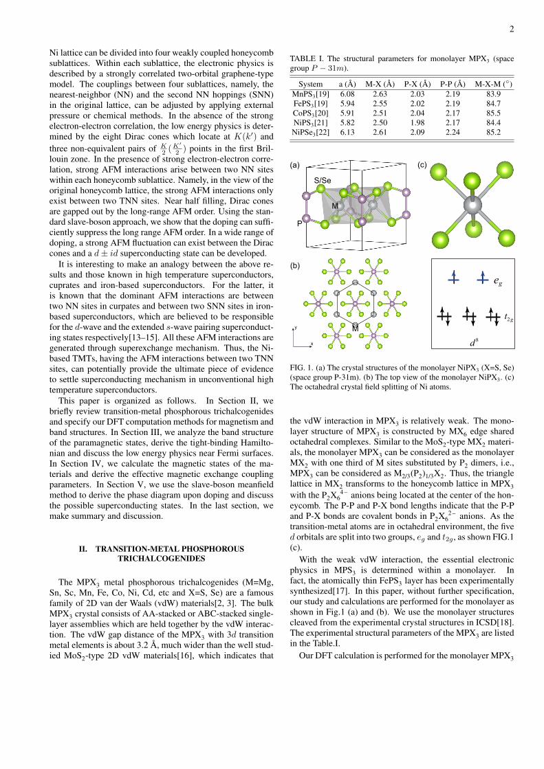
All the members in the family of ABX3 materials are builton a common structural unit, (P2X6)4 – (X=S, Se, Te) anioncomplex. However, the cation atom A is rather flexible, rang-ing from vanadium to zinc (A=V, Cr, Mn, Fe, Co, Ni, Zn, etc.)in the row of the 3d transition metal, partial alkaline metalin group-II, and some other metal ions. As shown in Fig.1(a,b), the cation is coordinated with six chalcogen anions toform an octehedra complex. In the two-dimensional layer,the cation forms a graphene-type honeycomb lattice. Thetransition-metal trichalcogenides exhibit a variety of intrigu-ing magnetically ordered insulating states[6]. Recently, underhigh pressure, FePSe3 can also become a superconductor[7].
Among this family of materials, the Ni-based trichalco-genides can carry intriguing electronic physics, such as strongcharge-spin coupling[8], because of the following reasons.First, as the transition metal cation and chalcogen anions forman octahedral complex, the 3d-orbitals of the transition metalare divided into high energy eg and low energy t2g groups.
In the case for Ni which has 8 electrons in the 3d-shell, thet2g orbitals are fully occupied and the two eg orbitals arehalf-filled as shown in Fig.1 (c). The t2g orbitals are inac-tive. The Ni-based trichalcogenides should be described by arelatively simpler low energy effective model than other ma-terials. Second, unlike a two dimensional square lattice, ahoneycomb lattice easily exhibits a Dirac-cone type of energydispersion. Near half filling, both one-orbital model, such asgraphene[1], and two-orbital models[9, 10] in the honeycomblattice are featured with Dirac points near Fermi energy. Withthe strong electron-electron correlation in the 3d-orbitals, theNi-based trichalcogenide thus can be a candidate of stronglycorrelated Dirac electron systems. It is worth to mentionthat a recent major research effort has aimed to increase theelectron-electron correlation in graphene[11], in which flatbands have to be engineered to observe correlation effects be-cause of p-orbitals. Finally, both density functional theory(DFT) calculation and experimental measurements have sug-gested that the Ni honeycomb lattice forms the zigzag antifer-romagnetic insulating ground state featured as double paral-lel ferromagnetic chains being anti-ferromagnetically (AFM)coupled[6, 12]. The material offers a promising platform tostudy the interplay between the low energy Dirac electronicphysics and the magnetism. Such an interplay is believed tobe responsible for many important phenomena, for example,high temperature superconductivity in both cuprates and iron-based superconductors[13, 14].
In this paper, we show that the Ni-based TMTs are Diracmaterials with strong electron-electron correlation. Their lowenergy electronic physics can be entirely attributed to the twoeg d-orbitals with a band kinematics dominated by an unusual”long-range” hoppings between two third nearest-neighbor(TNN) Ni sites in the Ni honeycomb lattice. Thus, the original
arX
iv:1
811.
0233
3v1
[co
nd-m
at.s
tr-e
l] 6
Nov
201
8
2
Ni lattice can be divided into four weakly coupled honeycombsublattices. Within each sublattice, the electronic physics isdescribed by a strongly correlated two-orbital graphene-typemodel. The couplings between four sublattices, namely, thenearest-neighbor (NN) and the second NN hoppings (SNN)in the original lattice, can be adjusted by applying externalpressure or chemical methods. In the absence of the strongelectron-electron correlation, the low energy physics is deter-mined by the eight Dirac cones which locate at K(k′) andthree non-equivalent pairs of K
2 (K′
2 ) points in the first Bril-louin zone. In the presence of strong electron-electron corre-lation, strong AFM interactions arise between two NN siteswithin each honeycomb sublattice. Namely, in the view of theoriginal honeycomb lattice, the strong AFM interactions onlyexist between two TNN sites. Near half filling, Dirac conesare gapped out by the long-range AFM order. Using the stan-dard slave-boson approach, we show that the doping can suffi-ciently suppress the long range AFM order. In a wide range ofdoping, a strong AFM fluctuation can exist between the Diraccones and a d± id superconducting state can be developed.
It is interesting to make an analogy between the above re-sults and those known in high temperature superconductors,cuprates and iron-based superconductors. For the latter, itis known that the dominant AFM interactions are betweentwo NN sites in curpates and between two SNN sites in iron-based superconductors, which are believed to be responsiblefor the d-wave and the extended s-wave pairing superconduct-ing states respectively[13–15]. All these AFM interactions aregenerated through superexchange mechanism. Thus, the Ni-based TMTs, having the AFM interactions between two TNNsites, can potentially provide the ultimate piece of evidenceto settle superconducting mechanism in unconventional hightemperature superconductors.
This paper is organized as follows. In Section II, webriefly review transition-metal phosphorous trichalcogenidesand specify our DFT computation methods for magnetism andband structures. In Section III, we analyze the band structureof the paramagnetic states, derive the tight-binding Hamilto-nian and discuss the low energy physics near Fermi surfaces.In Section IV, we calculate the magnetic states of the ma-terials and derive the effective magnetic exchange couplingparameters. In Section V, we use the slave-boson meanfieldmethod to derive the phase diagram upon doping and discussthe possible superconducting states. In the last section, wemake summary and discussion.
II. TRANSITION-METAL PHOSPHOROUSTRICHALCOGENIDES
The MPX3 metal phosphorous trichalcogenides (M=Mg,Sn, Sc, Mn, Fe, Co, Ni, Cd, etc and X=S, Se) are a famousfamily of 2D van der Waals (vdW) materials[2, 3]. The bulkMPX3 crystal consists of AA-stacked or ABC-stacked single-layer assemblies which are held together by the vdW interac-tion. The vdW gap distance of the MPX3 with 3d transitionmetal elements is about 3.2 A, much wider than the well stud-ied MoS2-type 2D vdW materials[16], which indicates that
TABLE I. The structural parameters for monolayer MPX3 (spacegroup P − 31m).
System a (A) M-X (A) P-X (A) P-P (A) M-X-M (◦)MnPS3[19] 6.08 2.63 2.03 2.19 83.9FePS3[19] 5.94 2.55 2.02 2.19 84.7CoPS3[20] 5.91 2.51 2.04 2.17 85.5NiPS3[21] 5.82 2.50 1.98 2.17 84.4NiPSe3[22] 6.13 2.61 2.09 2.24 85.2
P
S/Se
M
ge
2gt
8d
(a) (c)
(b)
x
y M
FIG. 1. (a) The crystal structures of the monolayer NiPX3 (X=S, Se)(space group P-31m). (b) The top view of the monolayer NiPX3. (c)The octahedral crystal field splitting of Ni atoms.
the vdW interaction in MPX3 is relatively weak. The mono-layer structure of MPX3 is constructed by MX6 edge sharedoctahedral complexes. Similar to the MoS2-type MX2 materi-als, the monolayer MPX3 can be considered as the monolayerMX2 with one third of M sites substituted by P2 dimers, i.e.,MPX3 can be considered as M2/3(P2)1/3X2. Thus, the trianglelattice in MX2 transforms to the honeycomb lattice in MPX3with the P2X 4 –
6 anions being located at the center of the hon-eycomb. The P-P and P-X bond lengths indicate that the P-Pand P-X bonds are covalent bonds in P2X 2 –
6 anions. As thetransition-metal atoms are in octahedral environment, the fived orbitals are split into two groups, eg and t2g , as shown FIG.1(c).
With the weak vdW interaction, the essential electronicphysics in MPS3 is determined within a monolayer. Infact, the atomically thin FePS3 layer has been experimentallysynthesized[17]. In this paper, without further specification,our study and calculations are performed for the monolayer asshown in Fig.1 (a) and (b). We use the monolayer structurescleaved from the experimental crystal structures in ICSD[18].The experimental structural parameters of the MPX3 are listedin the Table.I.
Our DFT calculation is performed for the monolayer MPX3

3
-2
-1
0
1
Γ K M Γ
Ene
rgy
(eV
)Ni dxz/yz
Ni dxy/x2-y2
Ni dz2
S p
-2
-1
0
1
Γ K M Γ
Ene
rgy
(eV
)
(a) Ni dxz/yz
Ni dxy/x2-y2
Ni dz2
Se pE
1A
2A
(b)
FIG. 2. Electronic band structures of (a) NiPS3 and (b) NiPSe3. Theorbital characters of bands are represented by different colors.
structures together with built-in 20 A thick vacuum lay-ers. We employ the Vienna ab initio simulation package(VASP) code[23] with the projector augmented wave (PAW)method[24] to perform the DFT calculations. The Perdew-Burke-Ernzerhof (PBE)[25] exchange-correlation functionalwas used in our calculations. Through out this work, the ki-netic energy cutoff (ENCUT) is set to be 500 eV for the ex-panding the wave functions into a plane-wave basis and the Γ-centered k-mesh is 16× 16× 1 for the nonmagnetic unit cell.The energy convergence criterion is 10−6 eV. We perform thestatic self-consistent calculation with the monolayer structurecleaved from the experimental crystal structures in ICSD[18].Since there is no experimental data about CuPS3 with this lay-ered hexagonal structure, we optimize CuPS3 with the forceconvergence criterion of 0.01 eV/A. In the study of effec-tive Hamiltonian, we employ Wannier90[26] to calculate thehopping parameters of the tight binding model. In the studyof magnetism of MPX3, the GGA plus on-site repulsion Umethod (GGA+U ) in the formulation of Dudarev et al.[27] isemployed to describe the associated electron-electron corre-lation effect. The effective Hubbard U (Ueff ) is defined byUeff = U − JHund. In order to describe different magneticorders, we build 2×1×1 supercell and the k-mesh is 8×16×1,correspondingly.
III. ELECTRONIC BAND STRUCTURES AND THETIGHT BINDING MODEL FOR NI-TRICHALCOGENIDES
In Fig.2, we plot the band structures of NiPS3 and NiPSe3,which are very similar to each other. From Fig.2, it is clearthat the five d-orbital bands are divided into two groups sep-arated by a large crystal field splitting energy. The groups atthe high and low energy are attributed to the two eg and threet2g orbitals respectively. The bands from t2g orbitals are com-pletely filled while the four bands from the two eg orbitals areclose to half-filling. This is consistent with the fact that theNi2+ cations are six-coordinated with an octahedral geometryand the d8 configuration in Ni2+ contributes two electrons tothe two eg orbitals. The physics near Fermi energy is con-trolled by the two eg dxz/yz orbitals. It is also worthy notingthat the contribution of the S/Se-p orbitals is considerable, es-
TABLE II. The NN, SNN and TNN hopping parameters and the bandwidths for NiPS3 and NiPSe3; xz and yz represent the band indexesof the hopping parameters.
NiPS3 NiPSe3
tNNxzxz (eV) -0.050971 -0.059617tNNyzyz (eV) -0.036294 -0.014879tSNNxzxz (eV) 0.012118 0.019696tSNNyzyz (eV) -0.015141 -0.017257tSNNxzyz (eV) 0.003175 0.003827tTNNxzxz (eV) -0.020218 -0.019138tTNNyzyz (eV) 0.238574 0.256818
band widths eg 0.89 1.01
TABLE III. The NN, SNN and TNN hopping parameters for NiPS3with different Ni-S-Ni angles; xz and yz represent the band indexesof the hopping parameters.
Ni-S-Ni (◦) 84.4 81.9 87.1tNNxzxz (eV) -0.050971 -0.038045 -0.066167tNNyzyz (eV) -0.036294 -0.026956 -0.040663tSNNxzxz (eV) 0.012118 0.011367 0.013838tSNNyzyz (eV) -0.015141 -0.009442 -0.021795tSNNxzyz (eV) 0.003175 0.001937 0.004137tTNNxzxz (eV) -0.020218 -0.021682 -0.019388tTNNyzyz (eV) 0.238574 0.210725 0.269932
pecially near Γ point, which indicates strong d-p hybridiza-tion.
Similar to the single orbital band structure in graphene, thetwo eg orbital bands are featured by Dirac points as well.Here, there are eight Dirac points which locate at K and K ′
points, as well as around K/2 and K ′/2 points along Γ-Kline as shown in Fig.2. These Dirac points are rather robust.To show the robustness, we analyze the symmetric characterof the bands, namely, their irreducible representations. Thetwo crossing bands along Γ-K line belong to A1 and A2 ir-reducible representations, and the bands at K points belongto E irreducible representation. Thus, the Dirac points areprotected by the symmetry as the bands belong to differentrepresentations.
In order to capture the two-dimensional electronic physicsnear the Fermi level, we construct the tight binding Hamilto-nian based on the two eg orbitals. The Hamiltonian can bewritten as
H0 =∑k
ψ†khkψk, (1)
where the basis ψ†k = (a†xk, a†yk, b
†xk, b
†yk) and
hk =
(ωk − µ γkγ†k ωTk − µ
)(2)
4
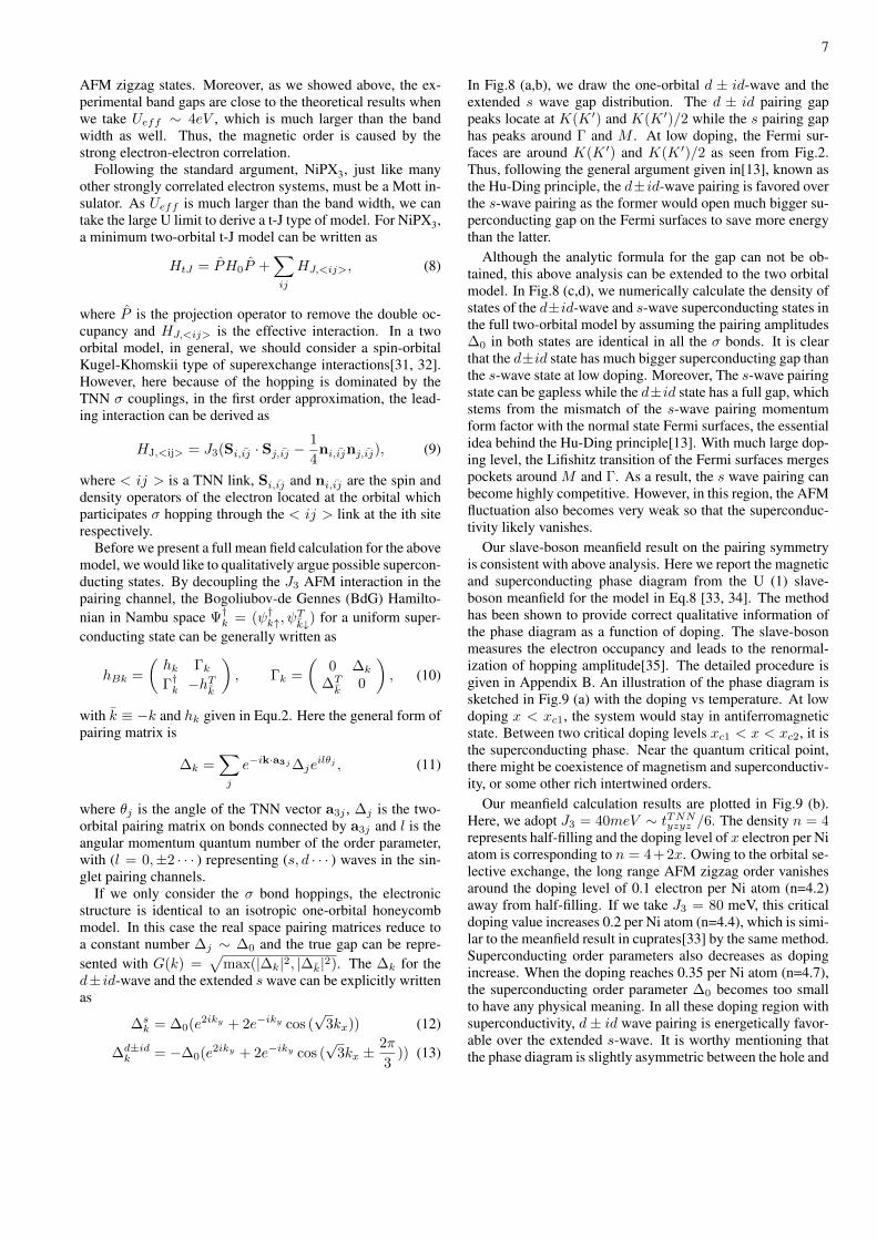
(b)(a)
FIG. 3. (a) The three NN, SNN, and TNN hopping parametersmarked by the green, brown and black dashed arrows, respectivelyand the zigzag AFM order with onsite red/blue arrows indicating spinup/down; (b) The four honeycomb sublattices.
with µ being the chemical potential and
ωk =∑j
e−ik·a1jTSNNj (3)
γk =∑j
e−ik·a2jTNNj + e−ik·a3jTSNNj . (4)
Here a†xk(b†yk) is the electron annihilator operator of orbitalxz(yz) in the usual A(B) sublattice of the honeycomb latticeand vectors a1,a2,a3 are the first, second and third neighborvectors. T ij = C3jT
iC−13j is the i-th neighbor hopping matrix
via the bond along ij bond direction and C3j is the threefoldrotation operation to the ij direction relative to the initial set-ting. T i(i = NN,SNN, TNN) is the hopping matrix withthe direction marked in Fig.3 (a):
T i =
(tixzxz tixzyz−ti∗xzyz tiyzyz
). (5)
By the lattice symmetry, tNNxzyz = tTNNxzyz = 0. We will useeV as the energy unit for all hopping parameters. The resultsof NiPS3 and NiPSe3 are similar, as shown in Table.II. Theexplicit formula of the Hamiltonian is given in Appendix A.Here we focus on the results of NiPS3.
It is interesting to notice that the leading term in the aboveHamiltonian is tTNNyzyz , the TNN σ-bond hoppings as shown inFig.3 (a), which is almost one order of magnitude larger thanthe other hopping parameters, namely, the NN and SNN hop-ping parameters. Thus, we can consider these TNN hoppingsas the dominant hopping parameters and treat other hoppingsas perturbations. In Fig.4 (a), we plot the band dispersion withonly the TNN hopping parameters. With only these TNN hop-pings, the original Ni honeycomb lattice is divided into fourdecoupled sublattices as shown in Fig.3 (b). Within each hon-eycomb sublattice, the model is identical to the one previouslystudied in an ultracold atomic honeycomb lattice with two de-generate p-orbitals[9, 10]. As shown in Fig.4 (a), there are twocompletely flat bands and two dispersive bands. The flat bandsstem from the localized binding and anti-binding molecularorbitals[9]. The two dispersive bands create the eight Diracpoints. With only these TNN hoppings, the second pair of
Γ K M ΓK/2 Γ K M ΓK/2
0.4
0.2
0.0
-0.2
-0.4
0.00.10.20.3
-0.1-0.2-0.3
Ene
rgy
(eV
)
Ene
rgy
(eV
)
(a) (b)
D1D2D2D1
D3 D3
D4D4
FIG. 4. The effect of different hopping parameters on the band struc-ture and Dirac points. (a) The band dispersion with only the leadingTNN hopping tTNNxzxz ; (b) The band dispersion with all hopping pa-rameters: the green, purple and black arrows represent the motionof the band and Dirac points by increasing the NN, SNN and TNNhopping parameters, respectively.
Q 1 Q 2
K
M
Γ
K`/24.2
3.8
5.0
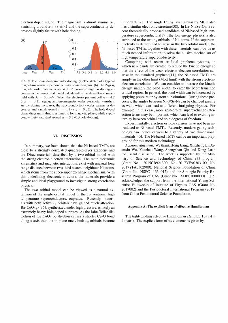
FIG. 5. Fermi surfaces and nesting vectors. The electron pocketsand hole pockets are marked by red and green respectively. The in-sets from top to bottom are Fermi surfaces at three doping levels , 0.1(electron), -0.1 (hole) and 0.5 (electron) per Ni atom with respect tothe half filling, corresponding to formula x = (n− 4)/2 with n thetotal electrons in each unit cell. In (a), nesting vectors Q1 and Q2
are depicted.
Dirac points are exactly located atK/2 andK ′/2 points. Thispair is simply created through the Brillouin zone folding be-cause of the sublattice structure. Thus, the presence of the twopairs of Dirac points underlines the sublattice structure.
The dominance of the tTNNyzyz in NiPX3 can be understoodfrom the lattice chemistry. The Ni-eg orbitals are stronglycoupled with S/Se-p orbitals. These effective hoppings aremediated through the central P2X 4 –
6 anion. For the NN hop-pings, two NN Ni atoms are in two edge shared MX6 octa-hedral complexes. As the Ni-X-Ni angle is close to 90◦, theNN indirect hopping through X is very small. The SNN ef-fective hopping is mediated by two S/Se atoms which sepa-rately locate in the top and bottom layers. The coupling be-tween these two S/Se atoms is weak due to the long distancearound 3.8A between them, which explains the weak SNN

5
hoppings. By contrast, the TNN σ hopping parameter is me-diated through two S/Se atoms in the same layer.
The effects of other hopping parameters on Dirac points andband structures are indicated in Fig.4 (b), in which the arrowsrepresent the motion of Dirac points and band structures whenthe corresponding hopping parameters increase. More specifi-cally, the weak third neighbor π-bond hoppings tTNNxzxz neitheraffect the Dirac cones atK andK/2, nor the band degeneracypoints at Γ and M . They only affect the flat bands in Fig.4 (a)far away from Fermi energy. The flat bands turn to dispersewhen tTNNxzxz increases. Therefore, in the weak hopping region,the low energy physics near Fermi surfaces are not affected bythe third neighbor π-bond hoppings. The weak second nearestneighbor hoppings, tSNNxzxz and tSNNyzyz , shift the Dirac points atK/2 and K vertically. By increasing these hoppings, the twoDirac points shift in opposite directions by a shift ratio equalto 3 as indicated by the purple arrows in Fig.4 (b). The weakNN hoppings, tNNxzxz and tNNyzyz , donot affect the Dirac cone atK because of the symmetry protection from the C3, time re-versal and inversion symmetries. However, it drags the K/2Dirac cone along Γ−K line as indicated by the green arrowsin Fig.4 (b). Band crossing pointsD3 andD4 are also draggedalong the direction indicated by the green arrows in Fig.2 (b).
The Fermi surfaces at the different doping levels are shownin Fig.5. Without the SNN hoppings, the model gives Diracsemimetals at half filling. Thus, the tiny pockets at half fillingshown in Fig.5 stem from very small SNN hoppings. Due tocharge conservation, the area of electron pockets at K/2 arethree times smaller than those hole pockets at K. In principle,with very small hole doping, strong nesting can take placebetween the electron and hole pockets at K and K ′/2 respec-tively, but not at K and K/2, by taking into consideration ofthe shapes of Fermi pockets. By increasing hole (electron)doping, both pockets at K and K/2 become hole (electron)pockets. When the doping reaches around 0.3 carriers per Niatoms, there is a Lifshitz transition of Fermi surfaces, namely,the two pockets emerge together to become one Fermi surface.
From the above Fermi surface topology, we can considerthe possible Fermi surface nesting in a paramagnetic state.Near half filling, the nesting vector is given by Q1 = G/2,half of the reciprocal lattice vector, as highlighted in Fig.5.This vector is exactly the ordered magnetic wavevector in theAFM zigzag state. We calculate the spin susceptibility underrandom phase approximation (RPA), with the same methodand notations specified in literature[28, 29]. The result is plot-ted in Fig.6 for several different doping levels. Clearly thesusceptibility peak emerges at M (Q1) near half filling. Be-low the critical doping at the Lifshitz transition, the peak iswell preserved, indicating the existence of strong AFM fluc-tuations.
IV. MAGNETIC EXCHANGE COUPLING PARAMETERSAND THE AFM ZIGZAG STATE
Without doping, MPX3 are known to be magneticinsulators[2, 3, 12, 30]. As the magnetic moments are local-ized at the transition metal atoms, the magnetism can be cap-
0
1
2
3
4
5
6
7
8χs
RPAχ0
0
1
2
3
4
5
6χs
RPAχ0
0
1
2
3
4
5
6χs
RPAχ0
0
1
2
3
4
5
6χs
RPAχ0
(a) (b)
(c) (d)
Γ K MK/2 Γ Γ K MK/2 Γ
Γ K MK/2 ΓΓ K MK/2 Γ
FIG. 6. Bare (dashed blue) and RPA (solid red) approximated spinsusceptibility for different doping levels: (a) half filling, (b) 0.1, (c)-0.1 and (d) 0.3 (Liftshiz point where K and K/2 pockets connect).Here the onsite energy U = 0.3eV and Hund’s coupling Jh = 0.2Uis adopted, similar to ref.[28]. Resonance apexes appear around thenesting vector Q1 (M) and Q2 (K/2) marked in Fig.5.
tured by an effective Heisenberg model with local magneticmoments. As the effect of the spin orbital coupling is gener-ally small for eg orbitals, we expect an isotropic Heisenbergmodel. Furthermore, from the lattice structure, it is obviousthat the minimum effective model should include NN, SNN,and TNN magnetic exchange coupling parameters. Namely,the model can be written as
H = J1
∑<ij>NN
~Si · ~Sj + J2
∑<ij>SNN
~Si · ~Sj+ J3
∑<ij>TNN
~Si · ~Sj . (6)
To extract the magnetic exchange coupling parameters, weconsider the following four different magnetic states: the fer-romagnetic (FM) state, the AFM Neel state, the AFM zigzagand the AFM stripy for MPS3 (M=Mn,Fe,Co,Ni,Cu) whichhave been synthesized experimentally. Those four magneticordering arrangements are shown in the review[2]. The AFMzigzag state is shown in Fig.3 (a). The results are shownin Table.IV. We find that the AFM Neel state is favored forMnPS3 and the AFM zigzag is favored for FePS3,CoPS3 andNiPS3, which is consistent with the experimental results inbulk MPS3 materials[6]. Our DFT calculation can give theinsulating states even without considering Ueff . With Ueffin GGA+U method, all four monolayer transition-metal phos-phorous trisulfides become AFM insulators, as shown in Ta-ble.IV. As a typical example, we plot the insulating bandstructure in the AFM zigzag state for NiPS3 in Fig.7 (a ). TheMn, Fe, Co and Ni atoms are in high spin states and the mag-netic moments slightly increase as Ueff increases. For bulkmaterials, the experimental band gaps are 3.0 eV, 1.5 eV and1.6 eV for Mn,Fe and Ni-based compounds, respectively[2].As shown in Table.IV, the calculated band gaps by GGA+Uat Ueff = 4eV are quantitatively close to the experimental

6
TABLE IV. The calculated ground state magnetic orders, magneticmoments and the band gaps for monolayer MPS3 (M = Mn, Fe, Co,Ni) using GGA+U (Ueff = 0 or 4eV).
Ueff = 0 Ground state magnetic order Moment (µB) Gap (eV)MnPS3 AFM Neel 4.26 1.43FePS3 AFM zigzag 3.32 0.01CoPS3 AFM zigzag 2.24 0.02NiPS3 AFM zigzag 1.13 0.79CuPS3 FM 0.24 0
Ueff = 4eV Ground state magnetic order Moment (µB) Gap (eV)MnPS3 AFM Neel 4.53 2.39FePS3 AFM zigzag 3.61 2.06CoPS3 AFM zigzag 2.57 1.85NiPS3 AFM zigzag 1.44 1.66CuPS3 FM 0.24 0
-2
-1
0
1
Γ K M Γ
Ener
gy (e
V)
Ni d
x2 2
Ni dxz/yz
Ni dxy/ -y
z2
S p
(a) (b)
Mn Fe Co Ni Cu-20
0
20
40
60
80
100
120
140 Ueff=0 eV Ueff=1 eV Ueff=2 eV Ueff=3 eV Ueff=4 eV
J3 (m
eV)
FIG. 7. (a) The band structure of NiPS3 in the AFM zigzag state.(b) J3 superexchange AFM interactions in MPS3 (M = Mn, Fe, Co,Ni, Cu), which are extracted from the GGA+U calculations with thevalues Ueff = (0, 1, 2, 3, 4)eV.
values.The classical energies of the four different magnetic states
for the effective Heisenberg model are given by
EFM = S2(6J1 + 12J2 + 6J3) + E0,
EAFM−Neel = S2(−6J1 + 12J2 − 6J3) + E0,
EAFM−zigzag= S2(2J1 − 4J2 − 6J3) + E0,
EAFM−stripy= S2(−2J1 − 4J2 + 6J3) + E0 (7)
From the calculated energies of these states, we can extractthe effective magnetic exchange interactions. The results arelisted in Table.V. Some similar results have been obtainedpreviously[12, 30]. Our calculation are consistent with theseprevious calculations[12, 30].
Here we pay special attention to the values in NiPX3. Asshown in Table.V, for NiPX3, among the three magnetic ex-change coupling parameters, J3 is one order of magnitudelarger than the other two parameters. Moreover, J3 is stronglyAFM while J1 and J2 both are weakly FM. These qualitativefeatures are independent of Ueff . The dominance of J3 overthe other two further confirms the extracted physical pictureof weakly coupled four sublattices as shown in Fig.3 (b) basedon the hopping parameters in the electronic band structure.J3 stems from so-called AFM super-superexchange
interaction[6, 30]. In Fig.7 (b), we plot the values of J3 asa function of M (M=Mn, Fe, Co, Ni, Cu). It is important to
TABLE V. The calculated exchange interaction parameters J1, J2and J3 for monolayer MPS3 (M = Mn, Fe, Co, Ni) and NiPSe3 usingGGA+U (Ueff = 0 or 4eV).
Ueff = 0 J1 (meV) J2 (meV) J3 (meV)MnPS3 4.69 0.40 2.03FePS3 -20.90 5.08 3.81CoPS3 -22.52 14.50 5.78NiPS3 -10.63 -2.30 131.24NiPSe3 -20.52 -4.38 215.55
Ueff = 4eV J1 (meV) J2 (meV) J3 (meV)MnPS3 1.62 0.09 0.61FePS3 -6.39 4.11 -1.90CoPS3 -1.71 -0.07 5.23NiPS3 -5.17 -0.78 34.93NiPSe3 -5.80 -0.45 53.13
note that for CuPS3, the AFM Neel and AFM zigzag states arenot metastable with different Ueff in our calculation, whichmeans that J3 ≤ 0. In Fig.7 (b), it is clear that J3 reachesthe maximum value in NiPX3, which can be easily under-stood as the hall-filling of eg orbitals maximize the super-superexchange interaction.
V. THE TWO-ORBITAL T-J MODEL AND DOPINGPHASE DIAGRAM FOR NIPX3
-20 -20-10 2010 2010-10E(meV) E(meV)
DOS(A.U.)
0
20
40
60
80
|∆0|(a)
0
3
1Г
KM M K
Г
K`/2 K`/22
0
20
40
60
80
+ d◇ s
++++++++++++++++++++++++++++++++++++++++++++++++++++++++++++++++++++++++++++++++++++++++++++++++++++++++++++++++++++++++++++++++++++++++++++++++++++++++++++++++++++++++++++++++++++++++
+++++++++++++++++++++++++++++++++++++++++++++++++++++++++++++++++++++++++ +++++++++++++++
+++++++++++++++++++++++++++++++++++++++++++++++++++++++++++++++++++++++++++++++++++++++++++++++++++++++++++++++++++++++++++++++++++++++++++++++++++++++++++++++++++++++++++++++++++++++++++++
+++++++++++++++++++++++++++++++++++++++
◇◇◇◇◇◇◇◇◇◇◇◇◇◇◇◇◇◇◇◇◇◇◇◇◇◇◇◇◇◇◇◇◇◇◇◇◇◇◇◇◇◇◇◇◇◇◇◇◇◇◇◇◇◇◇◇◇◇◇◇◇◇◇◇◇◇◇◇◇◇◇◇◇◇◇◇◇◇◇◇◇◇◇◇◇◇◇◇◇◇◇◇◇◇◇◇◇◇◇◇◇◇◇◇◇◇◇◇◇◇◇◇◇◇◇◇◇◇◇◇◇◇◇◇◇◇◇◇◇◇◇◇◇◇◇◇◇◇◇◇◇◇◇◇◇◇◇◇◇◇◇◇◇◇◇◇◇◇◇◇◇◇◇◇◇◇◇◇◇◇◇◇◇◇
◇◇◇◇◇◇◇◇◇◇◇◇◇◇◇◇◇◇◇◇◇◇◇◇◇◇◇◇◇◇◇◇◇◇◇◇◇◇◇
◇
◇
◇
◇◇◇◇◇◇◇◇◇◇◇◇
◇
◇
◇
◇
◇◇◇◇◇◇◇◇◇◇◇◇◇◇◇◇◇◇
◇◇◇◇
◇
◇
◇
◇
◇◇◇◇◇◇◇◇◇◇◇◇
◇
◇
◇
◇◇◇◇◇◇◇◇◇◇◇◇◇◇◇◇◇◇◇◇◇◇◇◇◇◇◇◇◇◇◇◇◇◇◇◇◇◇◇◇◇◇◇◇◇◇◇◇◇◇◇◇◇◇◇◇◇◇◇◇◇◇◇◇◇◇◇◇◇◇◇◇◇◇◇◇◇◇◇◇◇◇◇◇◇◇◇◇◇◇◇◇◇◇◇◇◇◇◇◇◇◇◇◇◇◇◇◇◇◇◇◇◇◇◇◇◇◇◇◇◇◇◇◇◇◇◇◇◇◇◇◇◇
◇◇◇◇◇◇◇◇◇◇◇◇◇◇◇◇◇◇◇◇◇◇◇◇◇◇◇◇◇◇◇◇◇◇◇
◇◇◇◇◇◇◇◇◇◇◇◇◇◇◇◇◇◇◇◇◇◇◇◇◇◇◇◇◇◇◇◇◇◇◇◇◇◇◇◇◇◇◇◇◇◇
+++++++++++++++++++++++++++++++ +++++++++++++++++++++++++++++++++++++++++++++++++++++++++++++++++++++++++++++++++++++++++++++
++++++++++++++++++++++++++++++++++++++++++++++++++++++++
+
+
+
+
++++++++++++++++++++++++++++++++++++++++++++++++++++++++++++++++ ++++++++++++++++++++ +++++++++++++
++++++++++++++++++++++++++++++++++
+
+
+
+
+++++++++++++++++++++++++++++++++++++++++++++++++++++++++++++++++++++++++++++++++++++++++++++++++++++++++++++++++++++++++++++++++++++++++++++++++++++++++++++++ ++++++++++++++++++++++◇◇◇◇◇◇◇◇◇◇◇◇◇◇◇◇◇◇◇◇◇◇◇◇◇◇◇◇◇◇◇◇◇◇◇◇◇◇◇◇◇◇◇◇◇◇◇◇◇◇◇◇◇◇◇◇◇◇◇◇◇◇◇◇◇◇◇◇◇◇◇◇◇◇◇◇◇◇◇◇◇◇◇◇◇◇◇◇◇◇◇◇◇◇◇◇◇◇◇◇◇◇◇◇◇◇◇◇◇◇◇◇◇◇◇◇◇◇◇◇◇◇◇◇◇◇◇◇◇◇◇◇◇◇◇◇◇◇◇◇◇◇◇◇◇◇◇◇◇◇◇◇◇◇◇◇◇◇◇◇◇◇◇◇◇◇◇◇◇◇◇◇◇◇◇◇◇◇◇
◇◇◇◇◇◇◇◇◇◇◇◇◇◇◇◇◇◇◇◇◇◇◇◇◇◇◇◇◇◇◇◇◇◇◇◇◇◇◇◇◇◇◇
◇
◇
◇
◇◇◇◇◇◇◇◇◇◇◇◇◇◇◇◇◇◇◇◇◇◇◇◇◇◇◇◇
◇◇◇◇◇◇◇◇◇◇◇◇◇◇
◇
◇
◇
◇◇◇◇◇◇◇◇◇◇◇◇◇◇◇◇◇◇◇◇◇◇◇◇◇◇◇◇◇◇◇◇◇◇◇◇◇◇◇◇◇◇◇◇◇◇◇◇◇◇◇◇◇◇◇◇◇◇◇◇◇◇◇◇◇◇◇◇◇◇◇◇◇◇◇◇◇◇◇◇◇◇◇◇◇◇◇◇◇◇◇◇◇◇◇◇◇◇◇◇◇◇◇◇◇◇◇◇◇◇◇◇◇◇◇◇◇◇◇◇◇◇◇◇◇◇◇◇◇◇◇◇◇◇◇◇◇◇◇◇◇◇◇◇◇◇◇◇◇◇◇◇◇◇◇◇◇◇◇◇◇◇◇◇◇◇◇◇◇◇◇◇◇◇◇◇◇◇◇◇◇◇◇◇◇◇◇◇◇◇◇◇◇◇◇◇◇◇◇◇◇◇◇◇◇◇◇◇◇◇◇◇◇◇◇◇◇◇◇◇◇◇◇
+ d◇ s
(b)
(c) (d)
FIG. 8. (a) and (b) plot the amplitude distributions of the supercon-ducting gap G(k) of the d± id-wave and the extended s-wave statesrespectively. (c) and (d) are the density of states in the d ± id-waveand the extended s-wave states at a doping level, n=3.8 and 4.2, re-spectively, by taking ∆0 = 0.3 and J3 = 40meV .
From the above analysis and the known experimentalfacts[6], it is clear that NiPX3 must belong to strongly cor-related electron systems. The band width of the two eg or-bitals is only about 1eV, much less than the band gaps in their
7
AFM zigzag states. Moreover, as we showed above, the ex-perimental band gaps are close to the theoretical results whenwe take Ueff ∼ 4eV , which is much larger than the bandwidth as well. Thus, the magnetic order is caused by thestrong electron-electron correlation.
Following the standard argument, NiPX3, just like manyother strongly correlated electron systems, must be a Mott in-sulator. As Ueff is much larger than the band width, we cantake the large U limit to derive a t-J type of model. For NiPX3,a minimum two-orbital t-J model can be written as
HtJ = PH0P +∑ij
HJ,<ij>, (8)
where P is the projection operator to remove the double oc-cupancy and HJ,<ij> is the effective interaction. In a twoorbital model, in general, we should consider a spin-orbitalKugel-Khomskii type of superexchange interactions[31, 32].However, here because of the hopping is dominated by theTNN σ couplings, in the first order approximation, the lead-ing interaction can be derived as
HJ,<ij> = J3(Si,ij · Sj,ij −1
4ni,ijnj,ij), (9)
where < ij > is a TNN link, Si,ij and ni,ij are the spin anddensity operators of the electron located at the orbital whichparticipates σ hopping through the < ij > link at the ith siterespectively.
Before we present a full mean field calculation for the abovemodel, we would like to qualitatively argue possible supercon-ducting states. By decoupling the J3 AFM interaction in thepairing channel, the Bogoliubov-de Gennes (BdG) Hamilto-nian in Nambu space Ψ†k = (ψ†k↑, ψ
Tk↓) for a uniform super-
conducting state can be generally written as
hBk =
(hk ΓkΓ†k −hTk
), Γk =
(0 ∆k
∆Tk
0
), (10)
with k ≡ −k and hk given in Equ.2. Here the general form ofpairing matrix is
∆k =∑j
e−ik·a3j∆jeilθj , (11)
where θj is the angle of the TNN vector a3j , ∆j is the two-orbital pairing matrix on bonds connected by a3j and l is theangular momentum quantum number of the order parameter,with (l = 0,±2 · · · ) representing (s, d · · · ) waves in the sin-glet pairing channels.
If we only consider the σ bond hoppings, the electronicstructure is identical to an isotropic one-orbital honeycombmodel. In this case the real space pairing matrices reduce toa constant number ∆j ∼ ∆0 and the true gap can be repre-sented with G(k) =
√max(|∆k|2, |∆k|2). The ∆k for the
d± id-wave and the extended s wave can be explicitly writtenas
∆sk = ∆0(e2iky + 2e−iky cos (
√3kx)) (12)
∆d±idk = −∆0(e2iky + 2e−iky cos (
√3kx ±
2π
3)) (13)
In Fig.8 (a,b), we draw the one-orbital d ± id-wave and theextended s wave gap distribution. The d ± id pairing gappeaks locate at K(K ′) and K(K ′)/2 while the s pairing gaphas peaks around Γ and M . At low doping, the Fermi sur-faces are around K(K ′) and K(K ′)/2 as seen from Fig.2.Thus, following the general argument given in[13], known asthe Hu-Ding principle, the d± id-wave pairing is favored overthe s-wave pairing as the former would open much bigger su-perconducting gap on the Fermi surfaces to save more energythan the latter.
Although the analytic formula for the gap can not be ob-tained, this above analysis can be extended to the two orbitalmodel. In Fig.8 (c,d), we numerically calculate the density ofstates of the d±id-wave and s-wave superconducting states inthe full two-orbital model by assuming the pairing amplitudes∆0 in both states are identical in all the σ bonds. It is clearthat the d±id state has much bigger superconducting gap thanthe s-wave state at low doping. Moreover, The s-wave pairingstate can be gapless while the d±id state has a full gap, whichstems from the mismatch of the s-wave pairing momentumform factor with the normal state Fermi surfaces, the essentialidea behind the Hu-Ding principle[13]. With much large dop-ing level, the Lifishitz transition of the Fermi surfaces mergespockets around M and Γ. As a result, the s wave pairing canbecome highly competitive. However, in this region, the AFMfluctuation also becomes very weak so that the superconduc-tivity likely vanishes.
Our slave-boson meanfield result on the pairing symmetryis consistent with above analysis. Here we report the magneticand superconducting phase diagram from the U (1) slave-boson meanfield for the model in Eq.8 [33, 34]. The methodhas been shown to provide correct qualitative information ofthe phase diagram as a function of doping. The slave-bosonmeasures the electron occupancy and leads to the renormal-ization of hopping amplitude[35]. The detailed procedure isgiven in Appendix B. An illustration of the phase diagram issketched in Fig.9 (a) with the doping vs temperature. At lowdoping x < xc1, the system would stay in antiferromagneticstate. Between two critical doping levels xc1 < x < xc2, it isthe superconducting phase. Near the quantum critical point,there might be coexistence of magnetism and superconductiv-ity, or some other rich intertwined orders.
Our meanfield calculation results are plotted in Fig.9 (b).Here, we adopt J3 = 40meV ∼ tTNNyzyz /6. The density n = 4represents half-filling and the doping level of x electron per Niatom is corresponding to n = 4 + 2x. Owing to the orbital se-lective exchange, the long range AFM zigzag order vanishesaround the doping level of 0.1 electron per Ni atom (n=4.2)away from half-filling. If we take J3 = 80 meV, this criticaldoping value increases 0.2 per Ni atom (n=4.4), which is simi-lar to the meanfield result in cuprates[33] by the same method.Superconducting order parameters also decreases as dopingincrease. When the doping reaches 0.35 per Ni atom (n=4.7),the superconducting order parameter ∆0 becomes too smallto have any physical meaning. In all these doping region withsuperconductivity, d± id wave pairing is energetically favor-able over the extended s-wave. It is worthy mentioning thatthe phase diagram is slightly asymmetric between the hole and
8
electron doped region. The magnetism is almost symmetric,vanishing around xc1 ≈ ±0.1 and the superconductivity de-creases slightly faster with hole doping.
(a)
xxx x x
T
SCSC
AFM
(b)
3.4 3.6 3.8 4.4 4.60
0.20.4
0.6
0.8
1.0
m/△
ndSCdSC Zi
gzag
AFM
ec1 ec2hc1hc2
▼
▼▼▼▼▼▼▼
◇◇
◇
◇
◇
◇◇◇◇
◇
◇◇◇
◇◇
▼
▼▼▼▼▼▼▼▼ ▼◇ ◇
4.2
FIG. 9. The phase diagram under doping. (a) The sketch of a typicalmagnetism versus superconductivity phase diagram. (b) The Zigzagmagnetic order parameter and d ± id pairing strength as doping in-creases in the two-orbital model calculated by the slave-Boson mean-field with J3 = 40meV . When the electrons per unit cell n = 4.2(xc1 = 0.1), zigzag antiferromagnetic order parameter vanishes.As the doping increases, the superconductivity order parameter de-creases and vanish around n = 4.7 (xc2 = 0.35). The hole dopedphase diagram is almost symmetric for magnetic phase, while super-conductivity vanished around n = 3.4 (0.3 hole doping).
VI. DISCUSSION
In summary, we have shown that the Ni-based TMTs areclose to a strongly correlated quadruple-layer graphene andare Dirac materials described by a two-orbital model withthe strong electron electron interaction. The main electronickinematics and magnetic interactions exist with unusual longrange distance between two third nearest neighbour Ni atoms,which stems from the super-super exchange mechanism. Withthis underlining electronic structure, the materials provide asimple and ideal playground to investigate strong correlationphysics.
The two orbital model can be viewed as a natural ex-tension of the single orbital model in the conventional hightemperature superconductors, cuprates. Recently, materi-als with both active eg orbitals have gained much attention.Ba2CuO3+δ[36], synthesized under high pressure, is likely anextremely heavy hole doped cuprates. As the Jahn-Teller dis-tortion of the CuO6 octahedron causes a shorter Cu-O bondalong c-axis than the in-plane ones, both eg orbitals become
important[37]. The single CuO2 layer grown by MBE alsohas a similar electronic structure[38]. In La2Ni2Se2O3, a re-cent theoretically proposed candidate of Ni-based high tem-perature superconductors[39], the low energy physics is alsoattributed to the two eg orbitals of Ni atoms. If the supercon-ductivity is determined to arise in the two orbital model, theNi-based TMTs, together with these materials, can provide usmuch needed information to solve the elusive mechanism ofhigh temperature superconductivity.
Comparing with recent artificial graphene systems, inwhich new bands are created to reduce the kinetic energy sothat the effect of the weak electron-electron correlation canarise in the standard graphene[11], the Ni-based TMTs aresimply in the other limit (Mott limit) with the strong electron-electron correlation. We can consider to increase the kineticenergy, namely the band width, to enter the Mott transitioncritical region. In general, the band width can be increased byapplying pressure or by atom substitutions. During these pro-cesses, the angles between Ni-S/Se-Ni can be changed greatlyas well, which can lead to different intriguing physics. Forexample, in this case, more spin-orbital superexchange inter-action terms may be important, which can lead to exciting in-terplay between orbital and spin degrees of freedom.
Experimentally, electron or hole carriers have not been in-troduced to Ni-based TMTs. Recently, modern gating tech-nology can induce carriers to a variety of two dimensionalmaterials[40]. The Ni-based TMTs can be an important play-ground for this modern technology.
Acknowledgement: We thank Hong Jiang, Xinzheng Li, Xi-anxin Wu, Yuechao Wang, Shengshan Qin and Dong Luanfor useful discussion. The work is supported by the Min-istry of Science and Technology of China 973 program(Grant No. 2015CB921300, No. 2017YFA0303100, No.2017YFA0302900), National Science Foundation of China(Grant No. NSFC-11334012), and the Strategic Priority Re-search Program of CAS (Grant No. XDB07000000). Q.Z.acknowledges the support from the International Young Sci-entist Fellowship of Institute of Physics CAS (Grant No.2017002) and the Postdoctoral International Program (2017)from China Postdoctoral Science Foundation.
Appendix A: The explicit form of effective Hamiltonian
The tight-binding effective HamiltonianH0 in Eq.1 is a 4×4 matrix. The explicit form of its elements is given by

9
H11 = tSNNxzxz (2 cos kx + coskx2
cos
√3ky2
) + tSNNyzyz coskx2
cos
√3ky2
,
H12 = tSNNxzxz (−√
3 sinkx2
sin
√3ky2
) + tSNNyzyz (√
3 sinkx2
sin
√3ky2
) + i(4tSNNxzyz sinkx2
(coskx2− cos
√3ky2
)),
H13 =1
2e− 2iky√
3
(e
12 i√
3ky cos
(kx2
)(tNNxzxz + 3tNNyzyz) + ei
√3ky (cos(kx)(tTNNxzxz + 3tTNNyzyz ) + 2tNNxzxz) + 2tTNNxzxz
),
H14 =1
2i√
3e− iky
2√
3
(sin
(kx2
)(tNNxzxz − tNNyzyz)− e
12 i√
3ky sin(kx)(tTNNxzxz − tTNNyzyz )
),
H22 = tSNNyzyz (2 cos kx + coskx2
cos
√3ky2
) + tSNNxzxz coskx2
cos
√3ky2
,
H24 =1
2e− 2iky√
3
(e
12 i√
3ky cos
(kx2
)(3tNNxzxz + tNNyzyz) + ei
√3ky (cos(kx)(3tTNNxzxz + tTNNyzyz ) + 2tNNyzyz) + 2tTNNyzyz
),
(A1)
with H23 = H14, H33 = H11, H34 = H∗12 and H44 = H22
by symmetry. These hopping parameters are given in Table.4in the main text.
Appendix B: Formulation of the slave boson meanfield
We provide the detailed procedure for the slave bosonmeanfield method on the Hamiltonian Eq. (8). In ourtwo orbital model, the two eg orbitals are degenerate sothat they have the identical occupancy. In the slave-bosonapproximation[35], the same occupancy for all the orbitalsleads to the same renormalization for all the hopping inter-action. Namely, we have
PH0P = |n4− 1|H0, (B1)
in which n = 4 ± 2x, x is the doped electron (+) or hole(-) per atom. n = 4 represents the half filling, where thekinetic energy vanishes and the Hamiltonian reduces to pureHeisenberg exchange interaction. The exchange term HJ,〈ij〉in Eq. (8) can be decoupled in superconducting and magneticchannels.
In superconducting channel, it is
−J3
2
∑ij
(〈∆†ij〉∆ij + ∆†ij〈∆ij〉
)+ Es, (B2)
with pairing matrix ∆†ij ≡ σa†iij,σ
a†jij,σ
with aiij,σ =
cos θijaix,σ + sin θijaiy,σ and the constant part
Es =J3
2
∑ij
(〈∆†ij〉〈∆ij〉+ niij,σnjij,σ
), (B3)
with the spin indices σ = −σ = ±1 and link ijthe TNN bond. The same spin coupling density termniij,σnjij,σ term in Es would be decoupled as bond hop-ping 〈a†
iij,σajij,σ〉aiij,σa
†jij,σ
according to the approach inliterature[33]. Those bond hopping terms effectively renor-malize the third neighbor σ-bond hoppings to affect the posi-tion and shape of Fermi surface. The hopping parameters and
Fermi surfaces will be renormalized as the doping varies inour model. Thus as a simple illustrating of the phase diagramunder slave boson method, those bond hopping terms wouldbe simply taken as the density correlation. Put the renormal-ized hopping and decoupled exchange terms together, in thetwo orbital momentum space, we obtain
∑k Ψ†khBkΨk +Es
with hBk given in Eq. (10).In the magnetic channel, the J3 dominated spin exchange
interaction prefers the zigzag AFM state as shown in Fig.3. Inthe mean field level, the magnetic order in the zigzag patternis given by < Si >= (−1)i2m0z with i = i1a21 + i2a22.It is important to point out that as only the σ bond orbitalsare considered, the spin exchange is orbital selective. That isto say, the spin operator, Si,ij = 1
2a+iijµ
σµνaiijν with σ thevector of three Pauli matrices. As a result
〈Szi,ij〉 = cos2 θijmixx + sin2 θijmiyy (B4)
+ cos θij sin θij(mixy +miyx),
with miαβ ≡ 〈σ(a†iασaiβσ))〉/2 = (−1)i2mαβ . Up to a con-stant term, HJ,〈ij〉 is decoupled as∑
HJ,〈ij〉 =∑k
σa†kασM2αβak+Q1βσ (B5)
with Q1 = G2/2 marked in Fig.5 as the ordered magneticwavevector. The scattering matrix from k to k + Q1 in egorbitals space is
M2 = −3J3
16
(3mxx +myy mxy +myx
mxy +myx mxx + 3myy
). (B6)
Defining Ψ†Mk = (Ψ†k,Ψ†k+Q1
), the meanfield Hamiltoniancan be written as
H =∑
k∈rBZ
(Ψ†MAkΨMk + tr(hk + hk+Q1)− 8µ
)+ Esm,
(B7)
with rBZ represent the reduced Brillouin zone due to magnetic

10
cell and Ak is a 16× 16 matrix as
Ak =
(hBk I2
⊗I2⊗M2
I2⊗I2⊗M†2 hBk+Q
)(B8)
EsmN
=3J3
2∆2
0 +3J3
8(3m2
xx + 3m2yy + 2mxxmyy (B9)
+ (mxy +myx)2 + n2).
In Ak, the first I2 is for particle-hole space and the secondis for A-B sublattice. The hBk is given in Eq. (10). Theself-consistency of the chemical potential is also taken intoconsideration for a fixed doping. It is easy to show that
nk + nk+Q1=8 + tr(Σ〈ΨMkΨ†Mk〉) (B10)
=8− tr(ΣUkf(Λk)U†k),
in which Σ is the 16×16 stagger matrix Σ ≡ −I2⊗σ3
⊗I4,
U†kAkUk = Λk, diagonalizes the Ak and f(Λk) is the Fermidistribution function.
It is worthy to mention that the numerical result indicatesslight difference between the intra-orbital magnetic orders,mxx and myy , due to the rotation symmetry breaking in theAFM zigzag state. The inter-orbital magnetic orders,mxy andmyx, are very small and can be ignored in the meanfield solu-tion.
[1] Novoselov, K. S. et al. Electric field effect in atomically thincarbon films. Science 306, 666–669 (2004).
[2] Wang, F. et al. New frontiers on van der waals layered metalphosphorous trichalcogenides. Adv. Funct. Mat. 28, 1802151(2018).
[3] Susner, M. A., Chyasnavichyus, M., McGuire, M. A., Ganesh,P. & Maksymovych, P. Metal thio-and selenophosphates asmultifunctional van der waals layered materials. Adv. Mater.29, 1602852 (2017).
[4] Friedel, C. Compt. Rend. 119 (1894).[5] Ferrand, L. Bull. Soc. Chim. 13, 115 (1895).[6] Le Flem, G., Brec, R., Ouvard, G., Louisy, A. & Segransan, P.
Magnetic interactions in the layer compounds MPX3 (M = Mn,Fe, Ni; X= X, Se). J. Phys. Chem. Sol. 43, 455–461 (1982).
[7] Wang, Y. et al. Emergent superconductivity in an iron-basedhoneycomb lattice initiated by pressure-driven spin-crossover.Nat. Commun. 9, 1914 (2018).
[8] Kim, So Yeun et al. Charge-Spin Correlation in van der WaalsAntiferromagnet NiPS3. Phys. Rev. Lett. 120, 136402 (2018).
[9] Wu, C., Bergman, D., Balents, L. & Sarma, S. D. Flat bands andwigner crystallization in the honeycomb optical lattice. Phys.Rev. Lett. 99, 070401 (2007).
[10] Wu, C. & Sarma, S. D. px,y-orbital counterpart of graphene:Cold atoms in the honeycomb optical lattice. Phys. Rev. B 77,235107 (2008).
[11] Cao, Y. et al. Correlated insulator behaviour at half-filling inmagic-angle graphene superlattices. Nature 556, 80 (2018).
[12] Chittari, B. L. et al. Electronic and magnetic properties ofsingle-layer MPX3 metal phosphorous trichalcogenides. Phys.Rev. B 94, 184428 (2016).
[13] Hu, J. & Ding, H. Local antiferromagnetic exchange and col-laborative fermi surface as key ingredients of high temperaturesuperconductors. Scientific Reports 2, 381 (2012).
[14] Hu, J. Identifying the genes of unconventional high temperaturesuperconductors. Science Bulletin 61, 561–569 (2016).
[15] Seo, K., Bernevig, B. A. & Hu, J. Pairing symmetry in a two-orbital exchange coupling model of oxypnictides. Phys. Rev.Lett. 101, 206404 (2008).
[16] Lebegue, S. & Eriksson, O. Electronic structure of two-dimensional crystals from ab initio theory. Phys. Rev. B 79,115409 (2009).
[17] Lee, J.-U. et al. Ising-type magnetic ordering in atomically thin
FePS3. Nano letters 16, 7433–7438 (2016).[18] Allmann, R. & Hinek, R. The introduction of structure types
into the inorganic crystal structure database icsd. Acta. Crystal-logr. A 63, 412–417 (2007).
[19] Ouvrard, G., Brec, R. & Rouxel, J. Structural determination ofsome MPS3 layered phases (M= Mn, Fe, Co, Ni and Cd). Mat.Res. Bull. 20, 1181–1189 (1985).
[20] Klingen, W., Eulenberger, G. & Hahn, H. Uber hexathio-und hexaselenohypodiphosphate vom typ MII
2 P2X6. Naturwis-senschaften 55, 229–230 (1968).
[21] Rao, R. R. & Raychaudhuri, A. Magnetic studies of a mixedantiferromagnetic system Fe1−xNixPS3. J. Phys. Chem. Sol.53, 577–583 (1992).
[22] Brec, R., Ouvrard, G., Louisy, A. & Rouxel, J. Proprietes struc-turales de phases M (II)PX3 (X= S, Se ). In Annales de chimie–science des materiaux, 499–512 (1980).
[23] Kresse, G. & Furthmuller, J. Efficiency of ab-initio total energycalculations for metals and semiconductors using a plane-wavebasis set. Comp. Mat. Sci. 6, 15–50 (1996).
[24] Kresse, G. & Joubert, D. From ultrasoft pseudopotentials tothe projector augmented-wave method. Phys. Rev. B 59, 1758(1999).
[25] Perdew, J. P., Burke, K. & Ernzerhof, M. Generalized gradientapproximation made simple. Phys. Rev. Lett. 77, 3865–3868(1996).
[26] Mostofi, A. A. et al. wannier90: A tool for obtainingmaximally-localised wannier functions. Comp. Phys. Commun.178, 685–699 (2008).
[27] Dudarev, S. L., Botton, G. A., Savrasov, S. Y., Humphreys, C. J.& Sutton, A. P. Electron-energy-loss spectra and the structuralstability of nickel oxide: An LSDA+U study. Phys. Rev. B 57,1505 (1998).
[28] Li, Y. et al. Robust d-wave pairing symmetry in multiorbitalcobalt high-temperature superconductors. Phys. Rev. B 96,024506 (2017).
[29] Scalapino, D. J. A common thread: The pairing interaction forunconventional superconductors. Rev. Mod. Phys. 84, 1383–1417 (2012).
[30] Wildes, A. et al. Magnetic structure of the quasi-two-dimensional antiferromagnet nips 3. Phys. Rev. B 92, 224408(2015).
[31] Castellani, C., Natoli, C. R. & Ranninger, J. Magnetic structure

11
of V2O3 in the insulating phase. Phys. Rev. B 18, 4945–4966(1978).
[32] Kugel, K. & Khomskii, D. The Jahn-Teller effect and mag-netism: transition metal compounds. Physics-Uspekhi 25, 231(1982).
[33] Wang, Q.-H., Lee, D.-H. & Lee, P. A. Doped t − J model ona triangular lattice: Possible application to NaxCoO2 · yH2Oand Na1−xTiO2. Phys. Rev. B 69, 092504 (2004).
[34] Brinckmann, J. & Lee, P. A. Renormalized mean-field theoryof neutron scattering in cuprate superconductors. Phys. Rev. B65, 014502 (2001).
[35] Ruegg, A., Indergand, M., Pilgram, S. & Sigrist, M. Slave-boson mean-field theory of the mott transition in the two-band
hubbard model. Eur. Phys. J. B 48, 55–64 (2005).[36] Li, W. et al. A new superconductor of cuprates with unique
features. arXiv:1808.09425 (2018).[37] Maier, T. A., Berlijn, T. & Scalapino, D. J. d-wave and s±
pairing strengths in Ba2CuO3+δ . arXiv:1809.04156 (2018).[38] Jiang, K., Wu, X., Hu, J. & Wang, Z. Nodeless high-
Tc superconductivity in highly-overdoped monolayer CuO2.arXiv:1804.05072 (2018).
[39] Le, C., Zeng, J., Gu, Y., Cao, G.-H. & Hu, J. A possible familyof Ni-based high temperature superconductors. Science Bulletin63, 957 – 963 (2018).
[40] Ye, J. T. et al. Liquid-gated interface superconductivity on anatomically flat film. Nat. Mater. 9, 125 (2009).