Göran Eriksson, ABB Corporate Research / COMSOL … · Academic research in fusion plasma physics...
22
Modeling of Complex Structures in El t ti T h l Göran Eriksson, ABB Corporate Research / COMSOL Conference 2009, Milan, Italy Electromagnetic Technology © ABB Group October 19, 2009 | Slide 1 Presented at the COMSOL Conference 2009 Milan
Transcript of Göran Eriksson, ABB Corporate Research / COMSOL … · Academic research in fusion plasma physics...
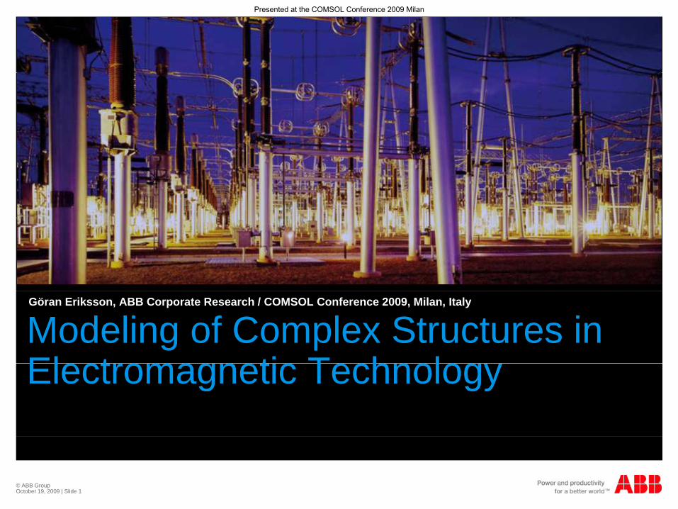
Modeling of Complex Structures in El t ti T h l
Göran Eriksson, ABB Corporate Research / COMSOL Conference 2009, Milan, Italy
Electromagnetic Technology
© ABB Group October 19, 2009 | Slide 1
Presented at the COMSOL Conference 2009 Milan
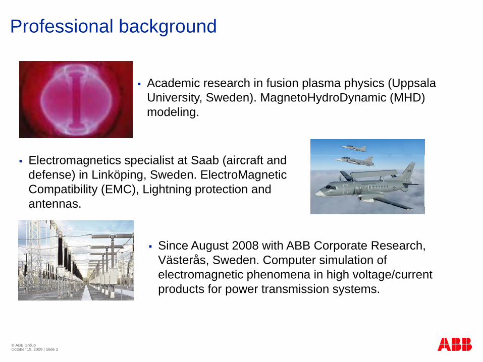
Professional background
Academic research in fusion plasma physics (Uppsala University, Sweden). MagnetoHydroDynamic (MHD) y ) g y y ( )modeling.
Electromagnetics specialist at Saab (aircraft and defense) in Linköping, Sweden. ElectroMagnetic Compatibility (EMC), Lightning protection and antennas.
Since August 2008 with ABB Corporate Research, Västerås Sweden Computer simulation of
antennas.
Västerås, Sweden. Computer simulation of electromagnetic phenomena in high voltage/current products for power transmission systems.
© ABB Group October 19, 2009 | Slide 2
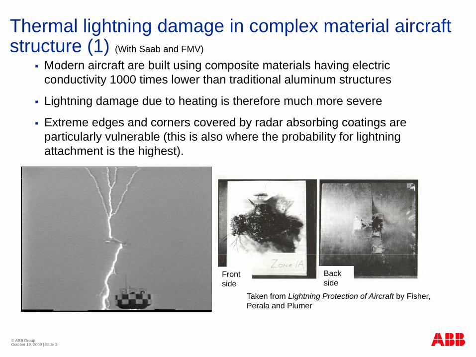
Thermal lightning damage in complex material aircraft structure (1) (With Saab and FMV)structure (1) (With Saab and FMV)
Modern aircraft are built using composite materials having electric conductivity 1000 times lower than traditional aluminum structures
Lightning damage due to heating is therefore much more severe Lightning damage due to heating is therefore much more severe
Extreme edges and corners covered by radar absorbing coatings are particularly vulnerable (this is also where the probability for lightning attachment is the highest)attachment is the highest).
Front side
Back side
Taken from Lightning Protection of Aircraft by Fisher, Perala and Plumer
© ABB Group October 19, 2009 | Slide 3
Perala and Plumer
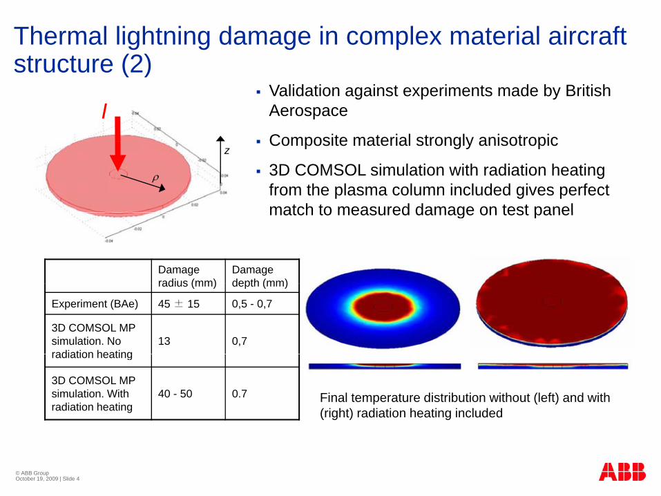
Thermal lightning damage in complex material aircraft structure (2)structure (2)
Validation against experiments made by British Aerospace
Composite material strongly anisotropicI
Composite material strongly anisotropic
3D COMSOL simulation with radiation heating from the plasma column included gives perfect match to measured damage on test panel
z
match to measured damage on test panel
Damageradius (mm)
Damagedepth (mm)radius (mm) depth (mm)
Experiment (BAe) 45 ± 15 0,5 - 0,7
3D COMSOL MP simulation. No radiation heating
13 0,7
Final temperature distribution without (left) and with (right) radiation heating included
radiation heating
3D COMSOL MP simulation. With radiation heating
40 - 50 0.7
© ABB Group October 19, 2009 | Slide 4
Thermal lightning damage in complex material aircraft structure (3)structure (3)
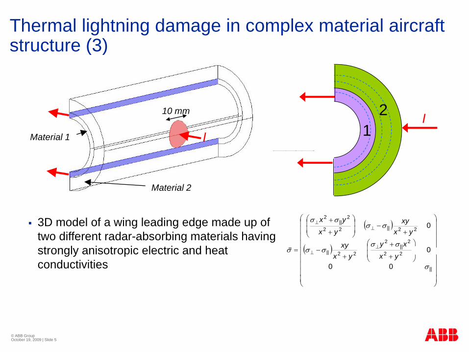
IMaterial 1
10 mmI2
1
Material 2
3D model of a wing leading edge made up of two different radar-absorbing materials having strongly anisotropic electric and heat
2||
2
||
22||22
2||
2
0
0
xyxy
yxxy
yx
yx
strongly anisotropic electric and heat conductivities
||
2222||
00
0
yxyx
© ABB Group October 19, 2009 | Slide 5
Thermal lightning damage in complex material aircraft structure (4)structure (4)
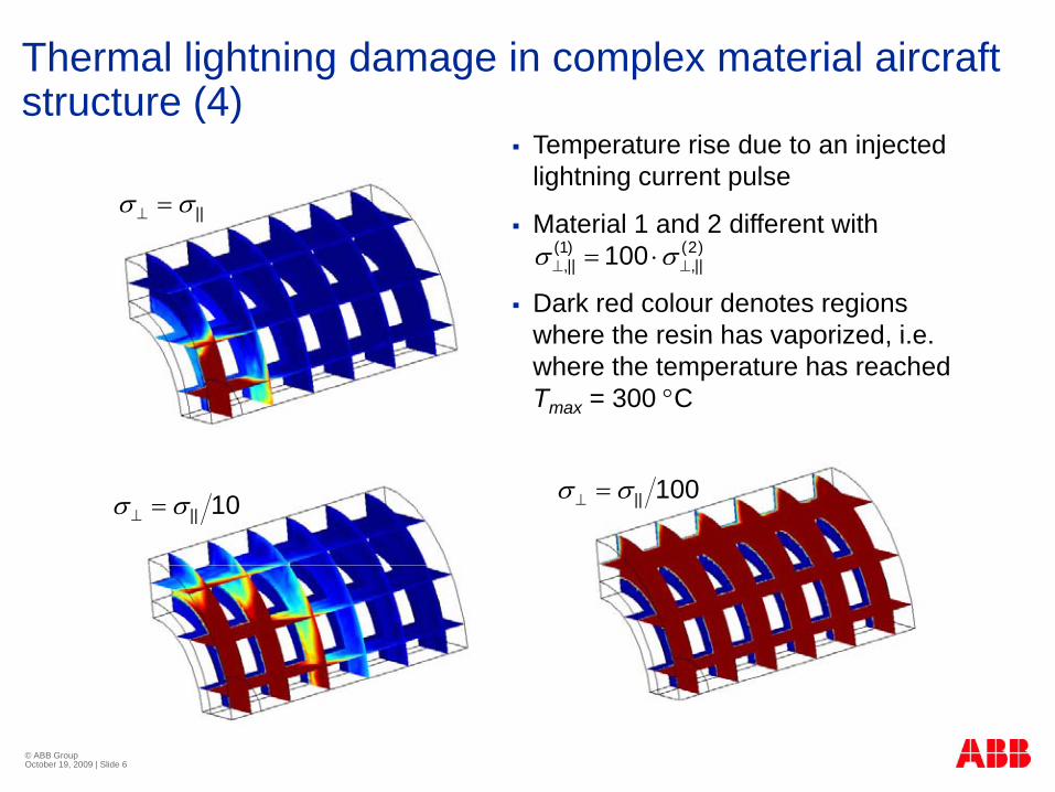
Temperature rise due to an injected lightning current pulse
Material 1 and 2 different with|| Material 1 and 2 different with
Dark red colour denotes regions where the resin has vaporized i e
)2(||,
)1(||, 100
where the resin has vaporized, i.e. where the temperature has reached Tmax = 300 C
100|| 10||
© ABB Group October 19, 2009 | Slide 6
Developing robust Frequency Selective Surface radome structures (1) (With Saab ACAB and FMV)radome structures (1) (With Saab, ACAB and FMV)
f ≠ f
f = f0
f ≠ f0
FSS radome
Antenna
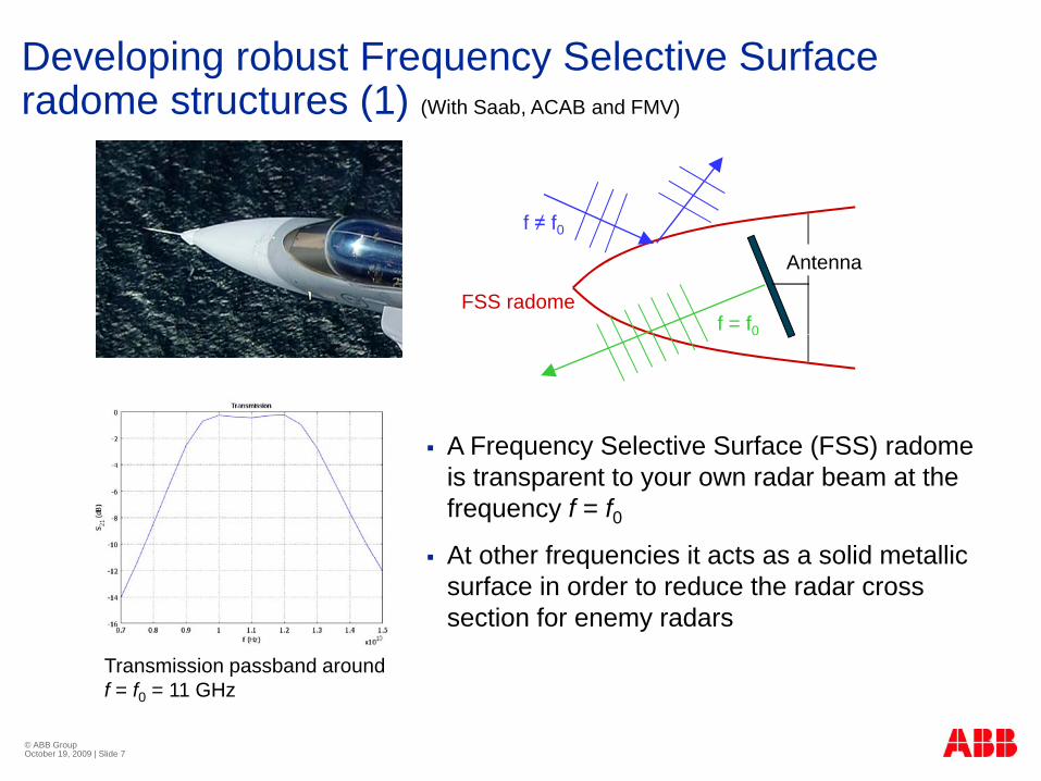
A Frequency Selective Surface (FSS) radome
0
A Frequency Selective Surface (FSS) radome is transparent to your own radar beam at the frequency f = f0
At other frequencies it acts as a solid metallic At other frequencies it acts as a solid metallic surface in order to reduce the radar cross section for enemy radars
Transmission passband around
© ABB Group October 19, 2009 | Slide 7
Transmission passband around f = f0 = 11 GHz
Developing robust Frequency Selective Surface radome structures (2)radome structures (2)
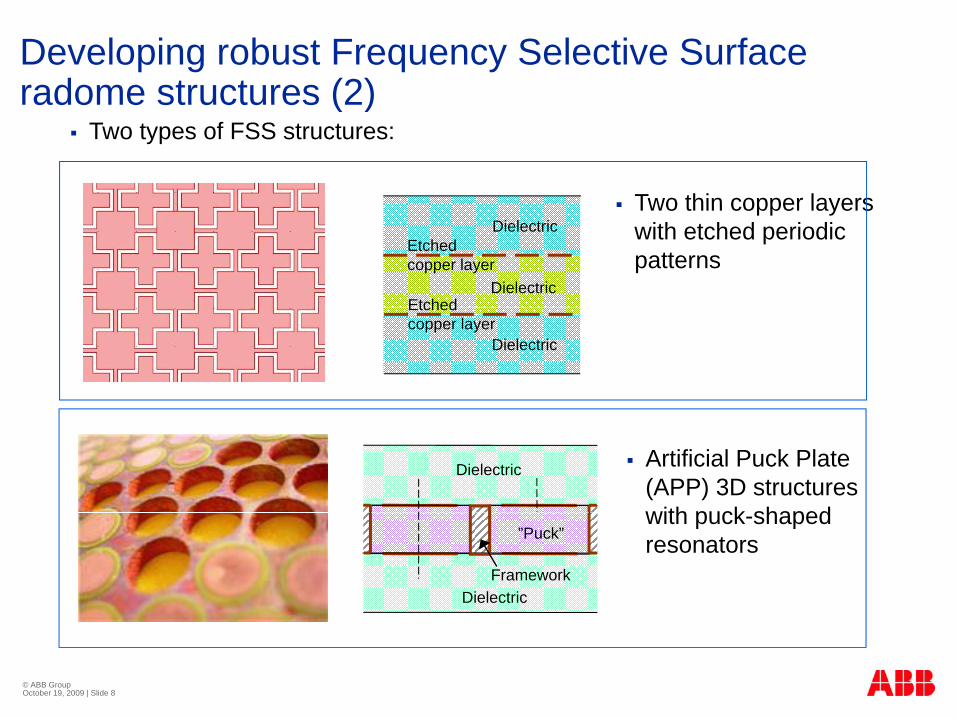
Two types of FSS structures:
Two thin copper layersDielectric
Dielectric
Etched copper layer
Etched
Two thin copper layers with etched periodic patterns
Dielectric
Etched copper layer
Dielectric Artificial Puck Plate (APP) 3D structures with puck shaped
”Puck”
FrameworkDielectric
with puck-shaped resonators
© ABB Group October 19, 2009 | Slide 8
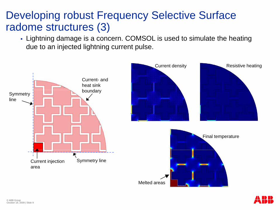
Developing robust Frequency Selective Surface radome structures (3)radome structures (3)
Lightning damage is a concern. COMSOL is used to simulate the heating due to an injected lightning current pulse.
Current- and heat sink bo ndar
Current density Resistive heating
Symmetry line
boundary
Final temperature
Symmetry lineCurrent injection area
© ABB Group October 19, 2009 | Slide 9
Melted areas
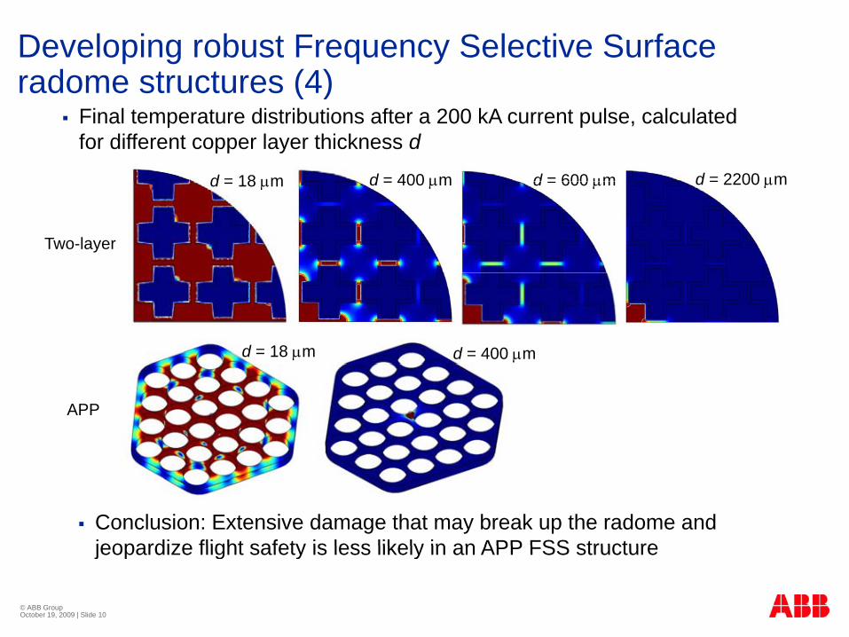
Developing robust Frequency Selective Surface radome structures (4)radome structures (4)
Final temperature distributions after a 200 kA current pulse, calculated for different copper layer thickness d
d = 18 m d = 400 m d = 600 m d = 2200 md = 18 m d = 400 m d = 600 m d 2200 m
Two-layer
d = 18 m d = 400 m
APP
Conclusion: Extensive damage that may break up the radome and jeopardize flight safety is less likely in an APP FSS structure
© ABB Group October 19, 2009 | Slide 10
jeopardize flight safety is less likely in an APP FSS structure
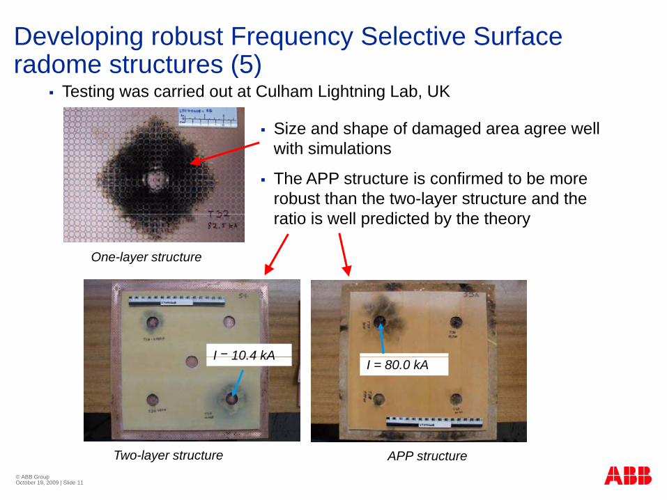
Developing robust Frequency Selective Surface radome structures (5)radome structures (5)
Testing was carried out at Culham Lightning Lab, UK
Size and shape of damaged area agree well ith i l tiwith simulations
The APP structure is confirmed to be more robust than the two-layer structure and the
ti i ll di t d b th th
One-layer structure
ratio is well predicted by the theory
I = 10 4 kAI 10.4 kAI = 80.0 kA
© ABB Group October 19, 2009 | Slide 11
Two-layer structure APP structure
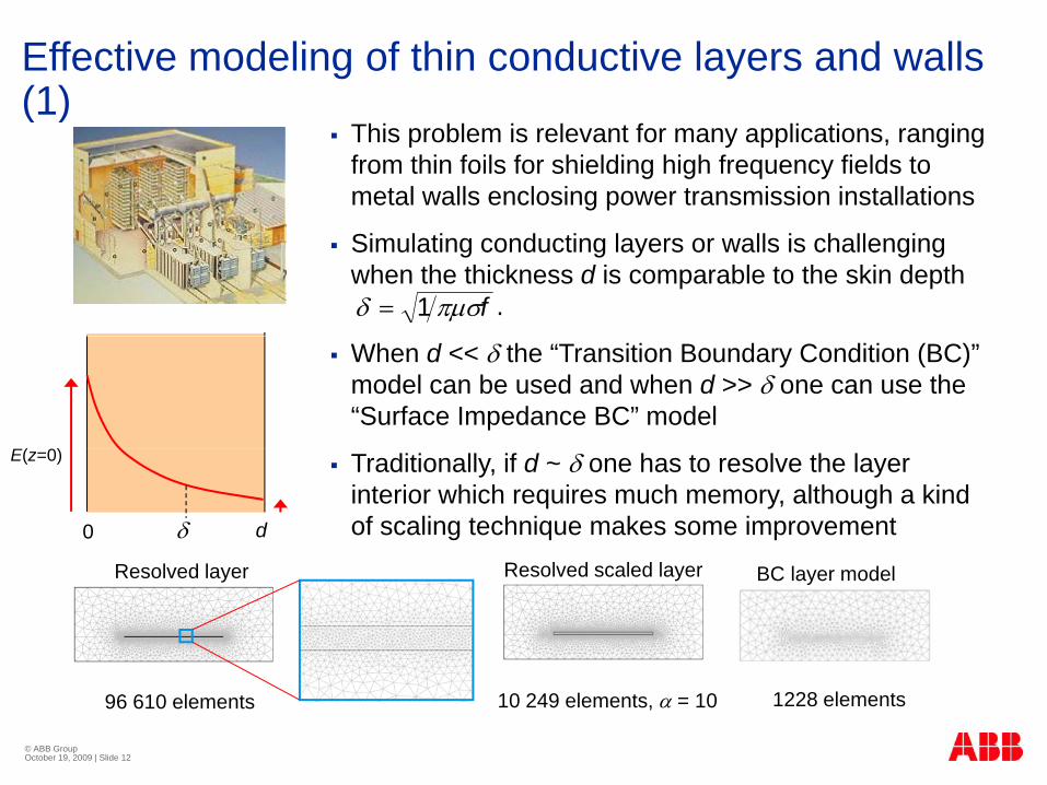
Effective modeling of thin conductive layers and walls (1)(1)
This problem is relevant for many applications, ranging from thin foils for shielding high frequency fields to metal walls enclosing power transmission installations
Simulating conducting layers or walls is challenging when the thickness d is comparable to the skin depth
.f 1
When d << the “Transition Boundary Condition (BC)” model can be used and when d >> one can use the “Surface Impedance BC” model
E( 0) Traditionally, if d ~ one has to resolve the layer
interior which requires much memory, although a kind of scaling technique makes some improvement
E(z=0)
0 d
Resolved layer Resolved scaled layer BC layer model
© ABB Group October 19, 2009 | Slide 12
96 610 elements 10 249 elements, = 10 1228 elements
Effective modeling of thin conductive layers and walls (2)(2)
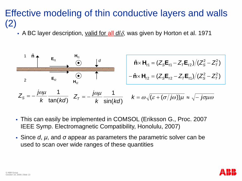
A BC layer description, valid for all d/, was given by Horton et al. 1971
1Et1
E
Ht1d
n̂)()(ˆ 22
211 TStTtSt ZZZZ EEHn
)()(ˆ 22122 TStTtSt ZZZZ EEHn
)tan(1kdk
jZS
)sin(
1kdk
jZT
jjk ))((
2 Et2 Ht2
)()( 122 TStTtSt ZZZZ EEHn
)( )(
This can easily be implemented in COMSOL (Eriksson G., Proc. 2007 IEEE Symp. Electromagnetic Compatibility, Honolulu, 2007)y p g p y, , )
Since d, μ, and σ appear as parameters the parametric solver can be used to scan over wide ranges of these quantities
© ABB Group October 19, 2009 | Slide 13
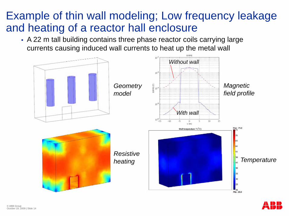
Example of thin wall modeling; Low frequency leakage and heating of a reactor hall enclosureand heating of a reactor hall enclosure
A 22 m tall building contains three phase reactor coils carrying large currents causing induced wall currents to heat up the metal wall
Without wall
Magnetic field profile
Without wall
Geometry model field profile
With wall
model
ResistiveResistive heating Temperature
© ABB Group October 19, 2009 | Slide 14
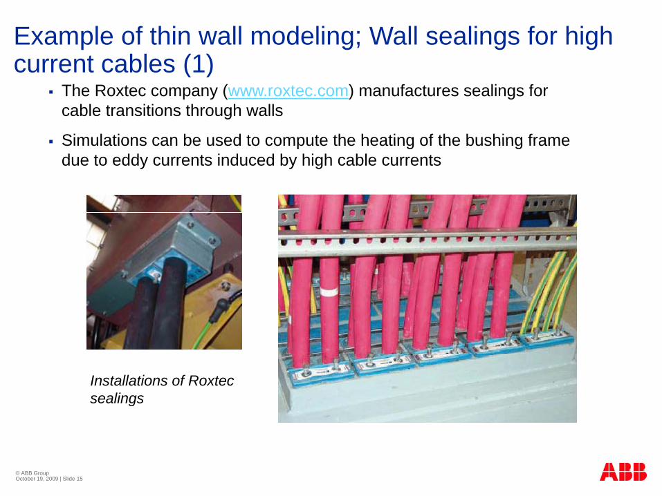
Example of thin wall modeling; Wall sealings for high current cables (1)current cables (1)
The Roxtec company (www.roxtec.com) manufactures sealings for cable transitions through walls
Simulations can be used to compute the heating of the bushing frame Simulations can be used to compute the heating of the bushing frame due to eddy currents induced by high cable currents
Installations of Roxtec sealings
© ABB Group October 19, 2009 | Slide 15
Example of thin wall modeling; Wall sealings for high current cables (2)current cables (2)
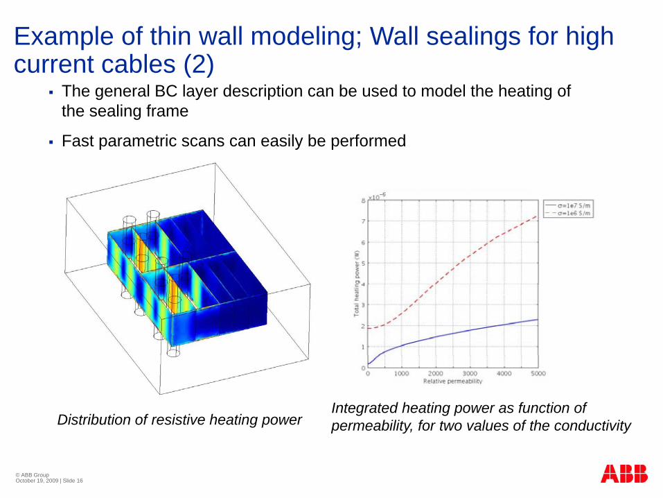
The general BC layer description can be used to model the heating of the sealing frame
Fast parametric scans can easily be performed Fast parametric scans can easily be performed
Distribution of resistive heating powerIntegrated heating power as function of permeability for two values of the conductivity
© ABB Group October 19, 2009 | Slide 16
g p permeability, for two values of the conductivity
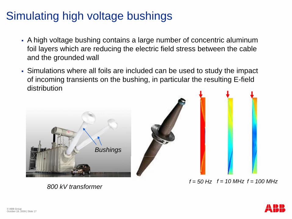
Simulating high voltage bushings
A high voltage bushing contains a large number of concentric aluminum foil layers which are reducing the electric field stress between the cable and the grounded wall
Simulations where all foils are included can be used to study the impact of incoming transients on the bushing, in particular the resulting E-field distribution
Bushings
800 kV transformerf = 100 MHzf = 50 Hz f = 10 MHz
© ABB Group October 19, 2009 | Slide 17
800 kV transformer
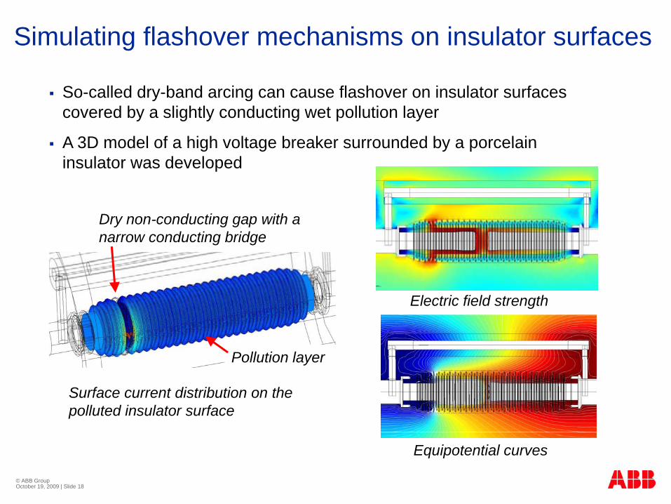
Simulating flashover mechanisms on insulator surfaces
So-called dry-band arcing can cause flashover on insulator surfaces covered by a slightly conducting wet pollution layer
A 3D model of a high voltage breaker surrounded by a porcelain A 3D model of a high voltage breaker surrounded by a porcelain insulator was developed
D d ti ithDry non-conducting gap with a narrow conducting bridge
Pollution layer
Electric field strength
Surface current distribution on the polluted insulator surface
Pollution layer
© ABB Group October 19, 2009 | Slide 18
Equipotential curves
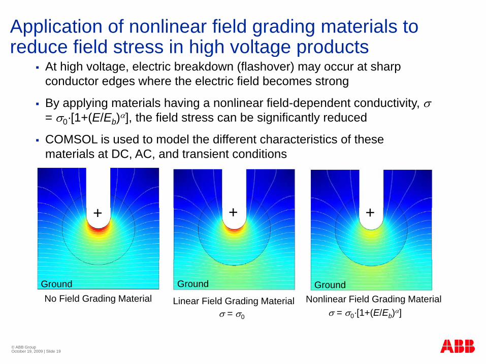
Application of nonlinear field grading materials to reduce field stress in high voltage productsreduce field stress in high voltage products
At high voltage, electric breakdown (flashover) may occur at sharp conductor edges where the electric field becomes strong
By applying materials having a nonlinear field-dependent conductivity By applying materials having a nonlinear field-dependent conductivity, = 0·[1+(E/Eb)], the field stress can be significantly reduced
COMSOL is used to model the different characteristics of these materials at DC AC and transient conditionsmaterials at DC, AC, and transient conditions
+ + +
No Field Grading Material Linear Field Grading Material Nonlinear Field Grading MaterialGround GroundGround
= [1+(E/E )]
© ABB Group October 19, 2009 | Slide 19
= 0·[1+(E/Eb)] = 0
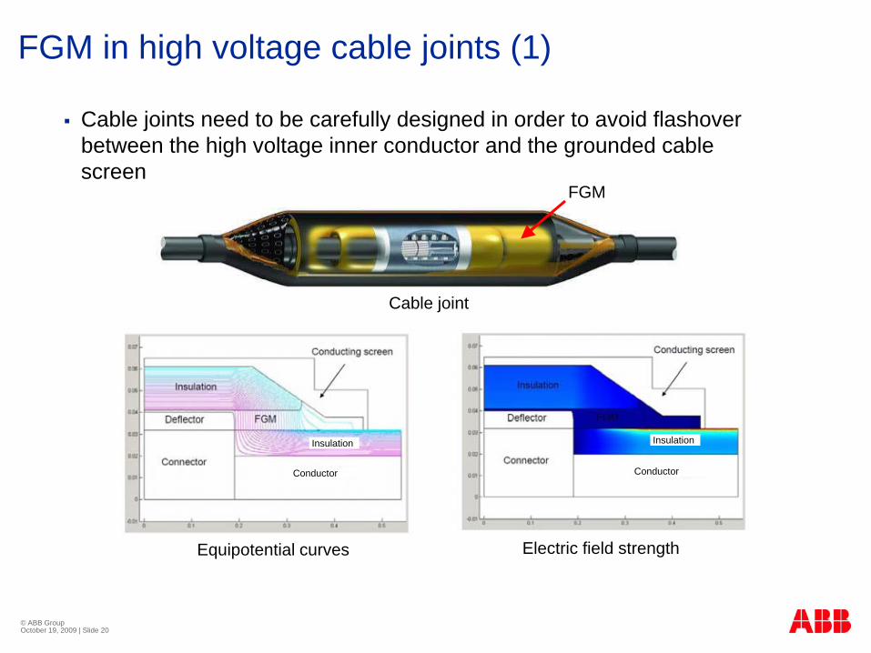
FGM in high voltage cable joints (1)
Cable joints need to be carefully designed in order to avoid flashover between the high voltage inner conductor and the grounded cable screen
FGMFGM
Cable joint
Insulation Insulation
Equipotential curves Electric field strength
Conductor Conductor
© ABB Group October 19, 2009 | Slide 20
Conclusions
In electromagnetic technology applications the finite element method is In electromagnetic technology applications the finite element method is very well suited for a wide range of problem types
For many cases, in particular when inhomogeneous materials having complex properties are involved as well as when multiphysics couplingscomplex properties are involved as well as when multiphysics couplings are essential, it is the only option available
The somewhat unfavourable performance scaling with problem size is becoming increasingly compensated by more powerful computers and beco g c eas g y co pe sated by o e po e u co pute s a dmore efficient solver routines
A technique to self-consistently include wires and slots, thinner than the element size, would be highly appreciated
© ABB Group October 19, 2009 | Slide 21
, g y pp

© ABB Group October 19, 2009 | Slide 22