
Getting started with STM32F373/378CC/RC/VC SDADC · PDF fileGetting started with...
31
July 2015 DocID26635 Rev 1 1/31 AN4550 Application note Getting started with STM32F373/378CC/RC/VC SDADC (Sigma-Delta ADC) Introduction The STM32F373/378xx microcontrollers embed three Sigma-Delta Analog to Digital Converter (SDADC). This innovative ADC type offers specific properties to extend the application range. The aim of this application note is to help understanding the SDADC principle, its properties and its features (explaining the functionalities), then compare SDADC with SAR type of ADC, and eventually help in choosing the correct ADC according to the addressed application. The document includes: • Overview of ADC types and their basic properties • SDADC principle explained in a simple way • SDADC advantages overview (from SDADC principle) • Oversampling and Digital filter - explanation of this digital block and its implementation • SDADC in STM32F373/378xx microcontrollers: summary of parameters • How to read the ADC parameters: Guide to choose the correct ADC for each application. www.st.com
-
Upload
nguyenthuy -
Category
Documents
-
view
232 -
download
0
Transcript of Getting started with STM32F373/378CC/RC/VC SDADC · PDF fileGetting started with...

July 2015 DocID26635 Rev 1 1/31
AN4550Application note
Getting started with STM32F373/378CC/RC/VC SDADC (Sigma-Delta ADC)
Introduction
The STM32F373/378xx microcontrollers embed three Sigma-Delta Analog to Digital Converter (SDADC). This innovative ADC type offers specific properties to extend the application range.
The aim of this application note is to help understanding the SDADC principle, its properties and its features (explaining the functionalities), then compare SDADC with SAR type of ADC, and eventually help in choosing the correct ADC according to the addressed application.
The document includes:
• Overview of ADC types and their basic properties
• SDADC principle explained in a simple way
• SDADC advantages overview (from SDADC principle)
• Oversampling and Digital filter - explanation of this digital block and its implementation
• SDADC in STM32F373/378xx microcontrollers: summary of parameters
• How to read the ADC parameters: Guide to choose the correct ADC for each application.
www.st.com

Contents AN4550
2/31 DocID26635 Rev 1
Contents
1 Introduction . . . . . . . . . . . . . . . . . . . . . . . . . . . . . . . . . . . . . . . . . . . . . . . . 6
1.1 ADC types . . . . . . . . . . . . . . . . . . . . . . . . . . . . . . . . . . . . . . . . . . . . . . . . . 6
2 SDADC overview . . . . . . . . . . . . . . . . . . . . . . . . . . . . . . . . . . . . . . . . . . . . 7
2.1 Basic principle . . . . . . . . . . . . . . . . . . . . . . . . . . . . . . . . . . . . . . . . . . . . . . 7
2.2 Sigma-Delta modulator . . . . . . . . . . . . . . . . . . . . . . . . . . . . . . . . . . . . . . . . 8
2.3 Sigma-Delta principal advantages . . . . . . . . . . . . . . . . . . . . . . . . . . . . . . 10
2.3.1 Noise shaping . . . . . . . . . . . . . . . . . . . . . . . . . . . . . . . . . . . . . . . . . . . . 10
2.3.2 Simpler anti-aliasing filter design . . . . . . . . . . . . . . . . . . . . . . . . . . . . . . 12
3 Sigma-Delta ADC basic properties . . . . . . . . . . . . . . . . . . . . . . . . . . . . 14
3.1 Advantages . . . . . . . . . . . . . . . . . . . . . . . . . . . . . . . . . . . . . . . . . . . . . . . 14
3.1.1 Excellent linearity . . . . . . . . . . . . . . . . . . . . . . . . . . . . . . . . . . . . . . . . . . 14
3.1.2 Scalable final resolution . . . . . . . . . . . . . . . . . . . . . . . . . . . . . . . . . . . . . 15
3.2 Disadvantages . . . . . . . . . . . . . . . . . . . . . . . . . . . . . . . . . . . . . . . . . . . . . 15
3.2.1 Gain error . . . . . . . . . . . . . . . . . . . . . . . . . . . . . . . . . . . . . . . . . . . . . . . . 15
3.2.2 Offset error . . . . . . . . . . . . . . . . . . . . . . . . . . . . . . . . . . . . . . . . . . . . . . . 15
3.2.3 Lower data rate . . . . . . . . . . . . . . . . . . . . . . . . . . . . . . . . . . . . . . . . . . . 15
4 Digital filter - part of Sigma-Delta ADC . . . . . . . . . . . . . . . . . . . . . . . . . 16
4.1 Function . . . . . . . . . . . . . . . . . . . . . . . . . . . . . . . . . . . . . . . . . . . . . . . . . . 16
4.2 Design . . . . . . . . . . . . . . . . . . . . . . . . . . . . . . . . . . . . . . . . . . . . . . . . . . . 16
4.2.1 Parameters . . . . . . . . . . . . . . . . . . . . . . . . . . . . . . . . . . . . . . . . . . . . . . 16
4.3 Digital filter - analysis . . . . . . . . . . . . . . . . . . . . . . . . . . . . . . . . . . . . . . . . 16
4.4 Digital filter – HW design basics . . . . . . . . . . . . . . . . . . . . . . . . . . . . . . . . 20
4.4.1 Basic averaging . . . . . . . . . . . . . . . . . . . . . . . . . . . . . . . . . . . . . . . . . . . 20
4.4.2 Simplification of schematic . . . . . . . . . . . . . . . . . . . . . . . . . . . . . . . . . . 20
4.4.3 Z-domain analysis . . . . . . . . . . . . . . . . . . . . . . . . . . . . . . . . . . . . . . . . . 21
4.4.4 Higher order CIC filters . . . . . . . . . . . . . . . . . . . . . . . . . . . . . . . . . . . . . 23
5 SDADC in STM32F373/378xx . . . . . . . . . . . . . . . . . . . . . . . . . . . . . . . . . 25
5.1 SDADC peripheral description . . . . . . . . . . . . . . . . . . . . . . . . . . . . . . . . . 25
5.1.1 SDADC from HW design . . . . . . . . . . . . . . . . . . . . . . . . . . . . . . . . . . . . 25

DocID26635 Rev 1 3/31
AN4550 Contents
3
5.1.2 SDADC precision characteristics overview . . . . . . . . . . . . . . . . . . . . . . 26
5.2 SDADC applications with STM32F373/378xx . . . . . . . . . . . . . . . . . . . . . 26
6 ADC parameters and their importance in different applications . . . . 27
6.1 Basic ADC electrical characteristics . . . . . . . . . . . . . . . . . . . . . . . . . . . . . 27
6.2 Static ADC parameters . . . . . . . . . . . . . . . . . . . . . . . . . . . . . . . . . . . . . . . 27
6.3 Dynamic ADC parameters . . . . . . . . . . . . . . . . . . . . . . . . . . . . . . . . . . . . 28
6.4 Typical ADC application guide . . . . . . . . . . . . . . . . . . . . . . . . . . . . . . . . . 28
7 Revision history . . . . . . . . . . . . . . . . . . . . . . . . . . . . . . . . . . . . . . . . . . . 30

List of tables AN4550
4/31 DocID26635 Rev 1
List of tables
Table 1. Critical ADC parameters . . . . . . . . . . . . . . . . . . . . . . . . . . . . . . . . . . . . . . . . . . . . . . . . . . . 28Table 2. Document revision history . . . . . . . . . . . . . . . . . . . . . . . . . . . . . . . . . . . . . . . . . . . . . . . . . 30

DocID26635 Rev 1 5/31
AN4550 List of figures
5
List of figures
Figure 1. ADC function. . . . . . . . . . . . . . . . . . . . . . . . . . . . . . . . . . . . . . . . . . . . . . . . . . . . . . . . . . . . . 6Figure 2. Sigma delta modulation (1-bit stream) . . . . . . . . . . . . . . . . . . . . . . . . . . . . . . . . . . . . . . . . . 7Figure 3. Sigma-Delta modulator diagram . . . . . . . . . . . . . . . . . . . . . . . . . . . . . . . . . . . . . . . . . . . . . . 8Figure 4. Sigma-Delta modulator schematics . . . . . . . . . . . . . . . . . . . . . . . . . . . . . . . . . . . . . . . . . . . 9Figure 5. Sigma-Delta modulator timing diagram . . . . . . . . . . . . . . . . . . . . . . . . . . . . . . . . . . . . . . . . 9Figure 6. Oversampled SAR ADC spectrum . . . . . . . . . . . . . . . . . . . . . . . . . . . . . . . . . . . . . . . . . . . 10Figure 7. Sigma-Delta modulator spectrum . . . . . . . . . . . . . . . . . . . . . . . . . . . . . . . . . . . . . . . . . . . . 10Figure 8. PWM modulation example . . . . . . . . . . . . . . . . . . . . . . . . . . . . . . . . . . . . . . . . . . . . . . . . . 11Figure 9. Sigma-Delta modulation example . . . . . . . . . . . . . . . . . . . . . . . . . . . . . . . . . . . . . . . . . . . . 12Figure 10. anti-aliasing filter design . . . . . . . . . . . . . . . . . . . . . . . . . . . . . . . . . . . . . . . . . . . . . . . . . . . 13Figure 11. Integral and differential linearities . . . . . . . . . . . . . . . . . . . . . . . . . . . . . . . . . . . . . . . . . . . . 14Figure 12. Example of simple 1-bit stream averaging . . . . . . . . . . . . . . . . . . . . . . . . . . . . . . . . . . . . . 17Figure 13. Additional steps between “1s” in higher order filtering . . . . . . . . . . . . . . . . . . . . . . . . . . . . 18Figure 14. Example of 3rd filter order outputs with Input higher . . . . . . . . . . . . . . . . . . . . . . . . . . . . . 19Figure 15. Example of 3rd filter order outputs with Input lower . . . . . . . . . . . . . . . . . . . . . . . . . . . . . . 19Figure 16. Schematic of implementation - 1 . . . . . . . . . . . . . . . . . . . . . . . . . . . . . . . . . . . . . . . . . . . . 20Figure 17. Schematic of implementation - 2 . . . . . . . . . . . . . . . . . . . . . . . . . . . . . . . . . . . . . . . . . . . . 21Figure 18. Reordered schematic (integrator stage as first) . . . . . . . . . . . . . . . . . . . . . . . . . . . . . . . . . 22Figure 19. Down sampling application . . . . . . . . . . . . . . . . . . . . . . . . . . . . . . . . . . . . . . . . . . . . . . . . . 23Figure 20. Final schematic of first order CIC filter . . . . . . . . . . . . . . . . . . . . . . . . . . . . . . . . . . . . . . . . 23Figure 21. Higher order CIC filter implementation . . . . . . . . . . . . . . . . . . . . . . . . . . . . . . . . . . . . . . . . 24

Introduction AN4550
6/31 DocID26635 Rev 1
1 Introduction
ADC is the acronym for Analog to Digital Converter. It converts an analog voltage into digital code (Figure 1).
Figure 1. ADC function
1.1 ADC types
The main ADC function can be achieved using different techniques, each one with specific properties.
Most commonly ADC types (with their typical properties):
• Successive approximation ADCs (SAR ADC)– Middle / fast speed, middle resolution
• Flash ADC (Parallel ADC)– Fast speed, lower resolution
• Sigma-Delta ADC (SDADC)– Low / middle speed, high resolution, good linearity
• Integrated ADC (Dual slope ADC)– Low speed, middle resolution, good linearity
• Others …
ADC requirements:
They must be identified to use the correct ADC in each application:
• Resolution– Number of bits in the output
• Accuracy– Number of valid bits in the output
• Sampling rate– Sampling frequency of the input data signal
• Speed (output data rate)– Frequency at which the ADC digital output is updated
• Oversampling– Ratio between sampling rate and output data rate
• Errors– Static: Linearity (differential, integral, total), Offset, Gain, Quantization, Total error– Dynamic: THD, SNR, SINAD, ENOB (note: ENOB is a dynamic parameter)

DocID26635 Rev 1 7/31
AN4550 SDADC overview
30
2 SDADC overview
2.1 Basic principle
The SDADC basic principle can be divided into two parts:
• Sigma-Delta modulation:– Very fast sampling rate of analog signal but with only 1-bit resolution.– Result is a 1-bit data stream, where the long duration average value represents the
analog input signal level (similar to PWM modulation). See Figure 2.
• Digital filter:– “Smart averaging” of the digital 1-bit data stream.– Result is higher resolution but lower data rate (oversampling + decimation).
Figure 2. Sigma delta modulation (1-bit stream)
Figure 2 is an example of an analog input signal and its corresponding bit-stream on the Sigma-Delta modulator output.

SDADC overview AN4550
8/31 DocID26635 Rev 1
2.2 Sigma-Delta modulator
A Sigma-Delta modulator is a circuit that generates a digital output with a 1-bit data stream from an analog input signal.
The output frequency isn’t constant (compared to PWM modulation), both frequency and duty cycle change.
Figure 3. Sigma-Delta modulator diagram
The principle of the first order Sigma-Delta modulator is shown in Figure 3. To better understand its operation, see Figure 4 and Figure 5, that illustrate the voltage levels at different stages of the modulator.
Figure 4 shows the Sigma-Delta modulator schematics.
The analog input signal [1] is added to the 1-bit DAC output (+Vref or -Vref voltage) fed back from the comparator and the result [2] goes to the integrator. The integrator output [3] is then compared with the zero level by the comparator. The comparator output [4] is latched periodically at the clock frequency by the D-latch to propagate the comparator result to the modulator output in quantized time steps (clock ticks). The D-latch output [5] is digital 1-bit output from the Sigma-Delta modulator. The output is fed back to the 1-bit D/A converter which has 2 analog output levels only (usually implemented as a switch between +Vref and Vref reference voltages). The data rate of the 1-bit output data stream is defined by the clock frequency.

DocID26635 Rev 1 9/31
AN4550 SDADC overview
30
Figure 4. Sigma-Delta modulator schematics
Figure 5. Sigma-Delta modulator timing diagram

SDADC overview AN4550
10/31 DocID26635 Rev 1
2.3 Sigma-Delta principal advantages
2.3.1 Noise shaping
This section describes the difference between the spectrum of standard k-times oversampled SAR ADC (see Figure 6) and the spectrum of Sigma-Delta modulator (see Figure 7).
From Figure 6 it can be seen that the quantization noise is spread evenly over the whole Nyquist bandwidth (up to kFs/2).
The digital filter removes noise above Fs/2. This noise suppression increases ADC resolution thanks to k-times oversampling.
Figure 6. Oversampled SAR ADC spectrum
Figure 7 shows the Sigma-Delta modulator output spectrum (Spectrum of 1-bit data stream from modulator output from Figure 2). It can be seen that much of the noise is moved toward the high frequencies (thanks to the integrator used in the Sigma-Delta modulator).
If an appropriate digital filter is used to filter 1-bit data stream then remaining noise is lower in comparison with SAR type ADC. The result is that oversampled Sigma-Delta modulation together with digital filtering can achieve better resolution than oversampled SAR ADC.
Figure 7. Sigma-Delta modulator spectrum

DocID26635 Rev 1 11/31
AN4550 SDADC overview
30
The noise spectrum shape comes directly from the Sigma-Delta modulation circuit. The 1-bit data stream result looks like PWM modulation and it has a variable frequency and duty cycle.
The Sigma-Delta modulator generates an output data stream with the highest possible frequency whereas PWM modulation has fixed frequency with variable duty cycle.
Example 1: 16-bit PWM
If the analog signal is at 50% of full scale then the 16-bit PWM modulation produces a signal with a 50% duty cycle at a fixed frequency: clock / 65536.
Example 2: Sigma-Delta modulator
If the analog signal is at 50% of full scale then the Sigma-Delta modulator in this case also produces a signal with 50% duty cycle but at the half clock frequency. As a consequence, the 1-bit data stream in the Sigma-Delta modulation has higher frequency content (especially if the analog signal is between 20%-80% of full scale, so that low duty cycle and therefore low frequency content is not generated). See Figure 8 and Figure 9. The advantage is easier design of the digital averaging filter to remove quantization noise.
Figure 8. PWM modulation example

SDADC overview AN4550
12/31 DocID26635 Rev 1
Figure 9. Sigma-Delta modulation example
2.3.2 Simpler anti-aliasing filter design
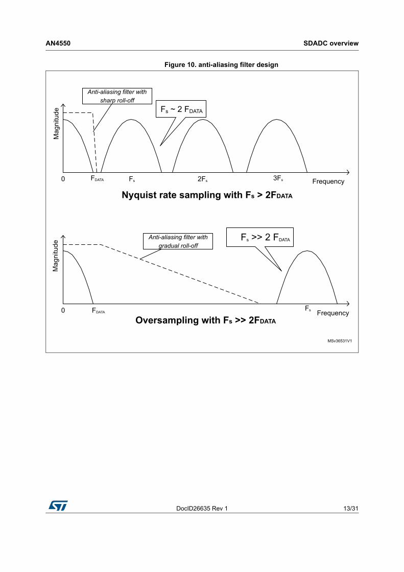
The sampling frequency (Fs) in the Sigma-Delta modulator is very high compared to the data bandwidth frequency (FDATA) due to the oversampling technique: Fs >> FDATA.
The design of an anti-aliasing filter to reject high frequencies and meet the Nyquist criteria is therefore very simple and cheap.
Figure 10 shows the cases of non-oversampled and oversampled ADC where the signal bandwidth is the same (same input signal) and the sampling frequency is Fs.
For non-oversampled ADC it is necessary to design a sharp filter roll-off to remove signals above frequency Fs/2. For the oversampled ADC (Sigma-Delta ADC) the design a simple lower order filter for Fs/2 image rejection is already sufficient.
DocID26635 Rev 1 13/31
AN4550 SDADC overview
30
Figure 10. anti-aliasing filter design

Sigma-Delta ADC basic properties AN4550
14/31 DocID26635 Rev 1
3 Sigma-Delta ADC basic properties
3.1 Advantages
3.1.1 Excellent linearity
A Sigma-Delta modulator generates a stream with 1-bit output data width. This 1-bit data stream is converted into a multi-bit output using a linear filter - a mathematically exact linear operation.
The transfer characteristics between analog and digital values is therefore linear: each data word output is a multiple of this 1-bit weight, ensuring excellent linearity over the whole input range compared to other ADC types. Static linearity errors (differential and integralnon-linearity) are therefore very low: DNL is ~0 (no missing codes), INL is lower than other ADC types.
An analog buffer can be used in front of Sigma-Delta modulator for high input impedance or to amplify the input analog signal. But this input buffer linearity influences the complete linearity of Sigma-Delta ADC.
Figure 11. Integral and differential linearities
The static parameter INL is linked to the dynamic THD parameter (total harmonic distortion). So THD is also very low for this ADC type. Remaining non-linearity is caused by non-ideal components used in the Sigma-Delta modulator (capacitors, comparator, resistors).
The low THD of the SDADC leads to its use for audio applications or any AC measurement applications sensitive to distortion.
DocID26635 Rev 1 15/31
AN4550 Sigma-Delta ADC basic properties
30
3.1.2 Scalable final resolution
The SDADC final resolution depends only on the digital filter parameters (order, length, filter type). The filter averages the 1-bit input stream to a parallel output with lower data rate.
A longer averaging time results in a higher resolution (e.g. 24-bit ADC) - but the drawback of increased resolution is a lower output data rate and longer latency (time to first sample output).
Example: 24-bit output @ 1kHz output data rate, 16-bit output @ 50kHz output data rate.
For this reason SDADC converters are used for very precise lower frequency measurement or DC measurement applications - such resolution cannot be easily offered by other ADC types.
3.2 Disadvantages
3.2.1 Gain error
The output data word weight is a multiple of the 1-bit weight (see Section 3.1.1). This 1-bit weight depends on the Sigma-Delta modulator components (among them capacitors and resistors of the integrator), so the full scale weight is not related only to the reference voltage (as for example in a SAR type ADC).
Sigma-Delta modulator component parameters (R, C, …) must be trimmed to produce full scale output data at full scale input analog signal (Vin = Vref). This is a hard to achieve through RC trimming, as 1% error results in a overall gain error of some percent points. This error means that at full scale output, the input voltage is not exactly equal to the reference voltage (up to ~5% of difference).
This disadvantage can be corrected by software calibration of the gain of each device (gain error can vary from device to device due to modulator component tolerance). The output data word is recalculated according to the calibrated real gain.
3.2.2 Offset error
The output zero code of the SDADC doesn’t need to correspond to 0V at the input. The reason is due to the Sigma-Delta modulator components (integrator offset, comparator offset, 1-bit DAC symmetry).
The solution is again in the implementation of software (or hardware) calibration (adding a calibration offset constant to the output data result).
3.2.3 Lower data rate
For proper filtering of 1-bit samples to reach higher output resolution, the use of a digital filter with higher oversampling ratio and higher order is needed, this leads to lower output data rate (decimation). So a bargain must be struck between resolution and speed for a given application area. In general SDADCs are focused on lower data rate applications with higher resolution.

Digital filter - part of Sigma-Delta ADC AN4550
16/31 DocID26635 Rev 1
4 Digital filter - part of Sigma-Delta ADC
4.1 Function
The digital filter is part of the SDADC (see Figure 3). It performs filtering (averaging) of the 1-bit data stream generated from the Sigma-Delta modulator. The filter output is a data word with increased resolution (usually 12 - 24 bits) but reduced data rate (decimation).
4.2 Design
The filter design has a big impact on the SDADC characteristics and is a compromise between the required parameters and hardware implementation complexity (cost issue). The goal is to design the filter with minimum complexity while meeting the required SDADC parameters.
Note: The signal filtering is more complex than simply the averaging of the 1-bit data stream. Averaging is the simplest filtering implementation but in practice a more complex function is required (see Section 4.3).
4.2.1 Parameters
Filter type
Various filter types can be used, for cheap hardware implementation the Sinc filter (synchronous frequency response) has been developed. The Sinc filter is the most commonly used type in SDADC implementations. It is cheap because no multipliers are required, and filter coefficients are only integers.
Filter length
A longer filter (averaging of more samples) generates higher resolution but decreases output data rate (decimation).
Filter order
A higher order filter generates higher resolution (by adding more averaging loops) but increases filter initialization time (need to fill whole filter with samples to start to produce output data).
4.3 Digital filter - analysis
Parameters of the SDADC in the STM32F373/378xx (using fixed filter parameters):
• Sampling clock of Sigma-Delta modulator: fin = 6 MHz
• Final output data rate: fout = 50 kHz (because of fixed decimation ratio = 120)fout = fin / 120
• Final resolution: 16 bits
When using simple averaging filter (first order Sinc filter) to reach a 16-bit resolution, 65536 bits have to be averaged using 1-bit data stream (see Figure 12). The output data rate will be 6 MHz / 65536 = 91.6 Hz only. To increase the data rate a more complex filter is required.

DocID26635 Rev 1 17/31
AN4550 Digital filter - part of Sigma-Delta ADC
30
Figure 12. Example of simple 1-bit stream averaging
More complex filters (with higher order Sinc filter, where order ≥ 2) increase the final data rate with the same resolution. Higher order Sinc filters perform the moving average more times in chaining (averaging of averaged data from previous filter stage).
Analysis of the higher order Sinc filter
The filtering now takes into account not only the number of ‘1s’ over a given duration (like simple averaging) but also their density in the data stream. This is thanks to the moving average implementation on each filter stage. Each filter stage is performing moving average over data from previous filter stage. At each cycle it performs the sum of the N values from previous stage outputs.
Explanation of resolution increase with given number of samples in stream
• An N-bit long Sigma-Delta modulated bit stream is applied to the filter input.
• A small analog value is applied to the Sigma-Delta modulator input - to get a simple ‘1’ at the end of the data stream (at the Nth position - see top of Figure 13).
• When the analog value increases slightly, we get one ‘1’ in the middle of the data stream and one ‘1’ at the end of the data stream (see bottom of Figure 13).
• In the transition between these two analog values (see again Figure 13) is the ‘1’ bit moving from the Nth to the (N/2)th position and then an additional ‘1’ appears at the end. (finally are there two bits in N-bit stream which represent higher analog value). Between those two states (on top and bottom of Figure 13) there are N/2 steps.
• So by recognizing position of this one '1' (in which position it is on given N-bit stream) is obtained additional N/2 resolution between 2 consecutive original values. Between one bit per period and 2 bits per period (between values 1/65536 and 2/65536) there are N/2 additional recognized values.
• The complete resolution will be then: N * N/2 = N2/2 (N is the length of the stream) because we added N/2 steps to original resolution (N). Stream length to achieve a 16-bit resolution will be: 65536 = N2/2 → N = 362 bits.

Digital filter - part of Sigma-Delta ADC AN4550
18/31 DocID26635 Rev 1
Figure 13. Additional steps between “1s” in higher order filtering
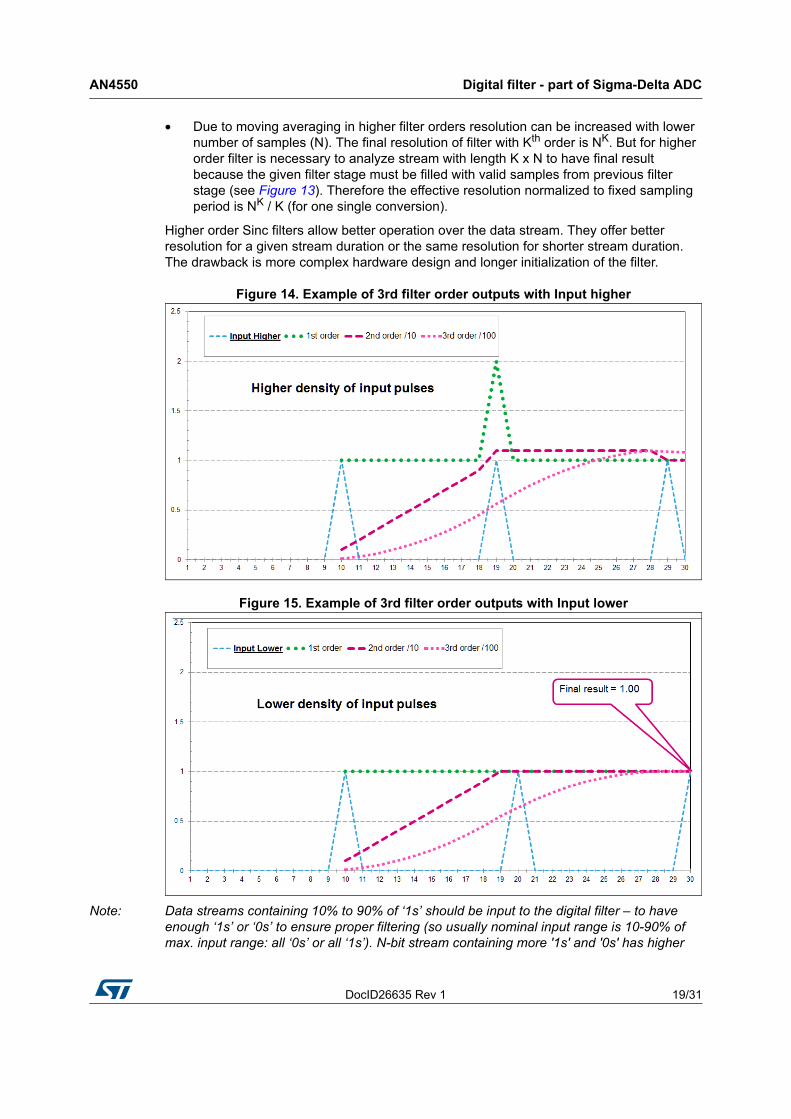
Practical explanation of 3rd order filter with N=10 (moving averaging of each filter stage):
• A 3rd order filter with oversampling N=10 must be analyzed with 3 periods of input stream: 3xN = 30 samples (see Figure 14 and Figure 15).
• In input stream in each averaging period (N=10) there is only one '1' (see the "Input" curves). There are tested 2 input streams: one with higher pulse density (Figure 14) and another with slightly lower pulse density (Figure 15).
• First order filter is performing moving average (see the “1st order” curves) and final result is sampled each Nth cycle as 1st order filter result (at 10th, 20th, 30th cycle). It always produces '1' as the final result on both stream cases because of simple filter (only one '1' in each period).
• Second order filter is performing moving average on samples from first filter order (see the “2nd order /10” curves). Its final result is sampled each Nth cycle as 2nd order filter result (at 20th, 30th cycle). There is visible difference in final results between the two streams: due to higher density of '1s' (in higher density stream) it produces higher value than in lower density stream.
• Third order filter is performing moving average on samples from second filter order (see the “3rd order /100” curves). Its final result is sampled each Nth cycle as 3rd order filter result (at 30th cycle). There is visible difference in final result between higher density stream and lower density stream. Due to moving averaging the output is smoother and more precise.
DocID26635 Rev 1 19/31
AN4550 Digital filter - part of Sigma-Delta ADC
30
• Due to moving averaging in higher filter orders resolution can be increased with lower number of samples (N). The final resolution of filter with Kth order is NK. But for higher order filter is necessary to analyze stream with length K x N to have final result because the given filter stage must be filled with valid samples from previous filter stage (see Figure 13). Therefore the effective resolution normalized to fixed sampling period is NK / K (for one single conversion).
Higher order Sinc filters allow better operation over the data stream. They offer better resolution for a given stream duration or the same resolution for shorter stream duration. The drawback is more complex hardware design and longer initialization of the filter.
Figure 14. Example of 3rd filter order outputs with Input higher
Figure 15. Example of 3rd filter order outputs with Input lower
Note: Data streams containing 10% to 90% of ‘1s’ should be input to the digital filter – to have enough ‘1s’ or ‘0s’ to ensure proper filtering (so usually nominal input range is 10-90% of max. input range: all ‘0s’ or all ‘1s’). N-bit stream containing more '1s' and '0s' has higher
Digital filter - part of Sigma-Delta ADC AN4550
20/31 DocID26635 Rev 1
frequency content spectrum and is more suitable for low pass filtering (see Figure 7, frequencies are filtered out).
Note: When starting filter operation fresh data should be input to the full filter to start generating valid output from a valid input data (“filter order” x “filter length” bits). The first sample is therefore delayed. Then in continuous operation mode is output data rate faster (each “filter length” bits) because filter is already filled with immediate valid previous data.
4.4 Digital filter – HW design basics
The following section describes in a simple manner the hardware design of a higher order Sinc filter. The explanation is divided into several steps to better understand the final implementation schematic.
4.4.1 Basic averaging
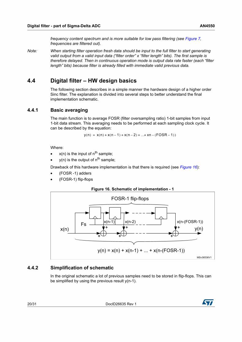
The main function is to average FOSR (filter oversampling ratio) 1-bit samples from input1-bit data stream. This averaging needs to be performed at each sampling clock cycle. It can be described by the equation:
Where:
• x(n) is the input of nth sample;
• y(n) is the output of nth sample;
Drawback of this hardware implementation is that there is required (see Figure 16):
• (FOSR -1) adders
• (FOSR-1) flip-flops
Figure 16. Schematic of implementation - 1
4.4.2 Simplification of schematic
In the original schematic a lot of previous samples need to be stored in flip-flops. This can be simplified by using the previous result y(n-1).
y n( ) x n( ) x n 1–( ) x n 2–( ) … xn FOSR 1–( ) )–+ + + +=

DocID26635 Rev 1 21/31
AN4550 Digital filter - part of Sigma-Delta ADC
30
The output y(n) at sample instant n is given by:
So if the previous output at sample instant n-1 is given by:
Then original equation can be simplified to:
or
The simplified schematic (Figure 17) is then described by equation:
Figure 17. Schematic of implementation - 2
Improvement and drawback (Figure 17.):
• with only 2 adders
• but still needed (FOSR+N) flip-flops
4.4.3 Z-domain analysis
The first order Sinc filter difference equation is:
To convert this into a different equation in discrete time domain, we can use the following correspondences:
• X(z)... in the Z-domain corresponds to x(n) in the discrete time domain, where n is an integer number of sample clock periods τ = 1/Fs
• z-N.X(z) ... corresponds to x(n-N) - which is x(n) delayed by N sample periods.
Transfer function H(z) for a 1-st order Sinc filter in Z-domain:
y n( ) x n( ) x n 1–( ) x n 2–( ) … x n FOSR 1–( )–( )+ + + +=
y n 1–( ) x n 1–( ) x n 2–( ) … x n FOSR 1–( )–( ) x n FOSR–( )+ + + +=
y n( ) x n( ) y n 1–( ) x n FOSR–( )–+=
y n( ) x n( ) x n FOSR–( )– y n 1–( )+=
y n( ) p n( ) y n 1–( ) where: p n( )+ x n( ) x n FOSR–( )–= =
y n( ) x n( ) x n FOSR–( )– y n 1–( )+=

Digital filter - part of Sigma-Delta ADC AN4550
22/31 DocID26635 Rev 1
From Figure 17. we can see that the left-hand “comb” stage is cascaded with right-hand “integrator” stage (therefore the name of this filter type is CIC filter: Cascaded integrator-comb filter). The comb transfer function in Z-domain is:
The integrator transfer function is:
The overall transfer function is equivalent to the Sinc filter transfer function:
In the next one will be explained how the design can be simplified. Firstly it is possible to reverse the order of the comb and integrator operation (integrator first):
The reordered schematic is shown in Figure 18.
Figure 18. Reordered schematic (integrator stage as first)
The next step of simplification is to down-sample the output y(n) by FOSR factor because the filtering limits the output signal bandwidth and so the output sampling rate can be reduced. This down-sampling is achieved by taking one sample of y(n) every FOSR clock cycles (see Figure 19.).
Y z( ) X z( ) zFOSR–
X⋅ z( )– z1–
Y z( )⋅+=
H z( ) Y z( )X z( )------------
1 zFOSR–
–
1 z1–
–-----------------------------= =
HC z( ) P z( )X z( )------------ 1 z
FOSR––= =
HI z( ) Y z( )P z( )------------
1
1 z1–
–-----------------= =
HC z( ) HI⋅ z( ) P z( )X z( )------------
Y z( )P z( )------------⋅ 1 z
FOSR––( ) 1
1 z1–
–-----------------⎝ ⎠
⎛ ⎞ 1 zFOSR–
–
1 z1–
–-----------------------------=⋅ H z( )= = =
H z( ) HI z( ) H⋅C
z( ) 1
1 z1–
–-----------------⎝ ⎠
⎛ ⎞ 1 zFOSR–
–( )⋅= =

DocID26635 Rev 1 23/31
AN4550 Digital filter - part of Sigma-Delta ADC
30
Figure 19. Down sampling application
The down-sampled clock period is defined as:
The difference equation for the down-sampled comb section can be rewritten:
This operation corresponds to a down-sampling of p(n) by FOSR, followed by a first order differentiator (comb part simplification). So the final schematic for N-bit output data width (see Figure 20.) is reduced to:
– 2 * N flip-flops (N ... output data bit-width)
– 2 adders (each with N-bit width)
Figure 20. Final schematic of first order CIC filter
4.4.4 Higher order CIC filters
In the previous section has been analyzed a first order CIC (Sinc) filter. To improve the resolution the filters can be cascaded.
TFOSR
Fs----------------- FOSR τ where: : τ T
FOSR-----------------=⋅= =
y n τ⋅( ) p n τ⋅( ) p n τ⋅ FOSR τ⋅–( )–=
yn T⋅
FOSR-----------------⎝ ⎠
⎛ ⎞ pn T⋅
FOSR-----------------⎝ ⎠
⎛ ⎞ pn T⋅
FOSR-----------------
FOSR T⋅FOSR
----------------------------–⎝ ⎠⎛ ⎞–=
y m( ) p m( ) p m 1–( ) where: : mn
FOSR-----------------=–=
Digital filter - part of Sigma-Delta ADC AN4550
24/31 DocID26635 Rev 1
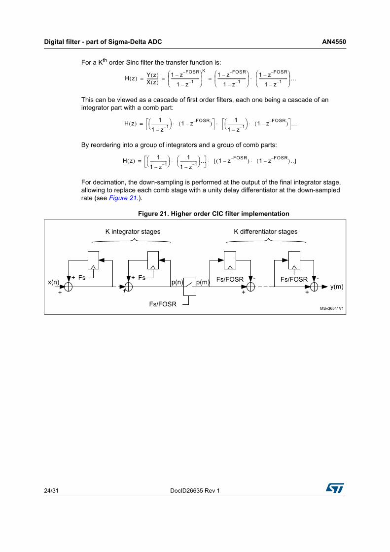
For a Kth order Sinc filter the transfer function is:
This can be viewed as a cascade of first order filters, each one being a cascade of an integrator part with a comb part:
By reordering into a group of integrators and a group of comb parts:
For decimation, the down-sampling is performed at the output of the final integrator stage, allowing to replace each comb stage with a unity delay differentiator at the down-sampled rate (see Figure 21.).
Figure 21. Higher order CIC filter implementation
H z( ) Y z( )X z( )------------
1 zFOSR–
–
1 z1–
–-----------------------------
⎝ ⎠⎜ ⎟⎛ ⎞ K
1 zFOSR–
–
1 z1–
–-----------------------------
⎝ ⎠⎜ ⎟⎛ ⎞ 1 z
FOSR––
1 z1–
–-----------------------------
⎝ ⎠⎜ ⎟⎛ ⎞
…⋅= = =
H z( ) 1
1 z1–
–-----------------⎝ ⎠
⎛ ⎞ 1 zFOSR–
–( )⋅ 1
1 z1–
–-----------------⎝ ⎠
⎛ ⎞ 1 zFOSR–
–( )⋅ …⋅=
H z( ) 1
1 z1–
–-----------------⎝ ⎠
⎛ ⎞ 1
1 z1–
–-----------------⎝ ⎠
⎛ ⎞ …⋅ 1 zFOSR–
–( ) 1 zFOSR–
–( )…⋅[ ]⋅=

DocID26635 Rev 1 25/31
AN4550 SDADC in STM32F373/378xx
30
5 SDADC in STM32F373/378xx
5.1 SDADC peripheral description
5.1.1 SDADC from HW design
In the STM32F373/378xx device ther are three ADCs based on the Sigma-Delta principle (SDADC1, SDADC2, SDADC3). From a hardware point of view these SDADCs have the following designed parameters:
• Resolution: 16 bits
– output data bit width
• ENOB = ~12.3 bits (gain=1), ~13.8 bits (gain=8)
– dynamic parameter representing AC performance of SDADC
• Input sampling rate (sigma delta modulator clock, SDADC clock):
– max. 6 MHz
– min. 0.5 MHz
• Speed (output data rate):
– max. 50 kHz
• Sinc filter:
– Oversampling ratio: FOSR = 120 (fixed)
– Order: K = 3 (fixed)
• Gains:
– Analog gains: 0.5, 1, 2, 4, 8
– Digital gains: 16, 32
• Offset calibration:
– Internal offset measurement when inputs are shorted
– Offset stored in register and used as correction
• Power supply:
– Independent analog supply pins (2 independent supplies for three SDADCs)
– VDDSDx = 2.4 V - 3.6 V (or 2.2 V for clock <1.5MHz)
– Consumption: 1200 / 600 / 200 / 2.5 / 1 µA (fast / slow / standby / power down / SDADC off)
• Reference voltage:
– External source: on VREFSD+ pin (VREFSD = 1.1 V - VDDSDx)
– Internal sources: Embedded internal reference: VREFINT = 1.2 V (or 1.5x amplified: 1.8 V)SDADC power supply as reference: VDDSDx
• Input impedance:
– Switched capacitor character (depends from selected SDADC clock and analog gain):47kΩ ... @6MHz, gain=868kΩ ... @6MHz, gain=1540kΩ ... @1.5MHz, gain=0.5

SDADC in STM32F373/378xx AN4550
26/31 DocID26635 Rev 1
5.1.2 SDADC precision characteristics overview
SDADCs in STM32F373/378xx reached following precision performance:
• Static parameters:
– Offset: ~100 µV
– Gain error: ~3%
– Differential non linearity (DNL): ~2.5 LSB
– Integral non linearity (INL): ~15 LSB
• Dynamic parameters:
– Total harmonic distortion (THD): ~ -77dB (gain = 1)
– Signal to noise ratio (SNR): 88dB (gain = 1)
– Signal to noise and distortion ratio (SINAD): 77dB (gain = 1), 85dB (gain=8)
– Effective number of bits (ENOB): ~12.5 bits (gain=1), ~13.8 (gain=8)
5.2 SDADC applications with STM32F373/378xx
Integrated SDADC converters in STM32F373/378xx device are suitable for applications with some of following needs:
• higher analog precision:
– (more than the internal 12-bit SAR ADC)
• lower frequency signals (audio range, DC measurement):
– DC measurements
– audio frequency range signals
• small signal levels measurement:
– integrated analog gains up to 8x
• differential measurements:
– differential inputs into ADC (“plus” and “minus” input pins)
• linear
– audio applications for lower distortion
Examples of applications are:
– DC sensors measurement (thermometers, pressure sensors, ...)
– audio recording (with ensuing Cortex®-M4 core computation power postprocessing)
– electricity meters (electric current measurement in a wide range)
– medical applications (ECG sensors, ...)
– industrial applications (motor controls, sensors, ...)
– All applications which require higher ADC precision, not so fast, lower signal measurement together with fast digital data post-processing featured by STM32F373/378xx (Cortex®-M4 core with DSP instructions and FPU)

DocID26635 Rev 1 27/31
AN4550 ADC parameters and their importance in different applications
30
6 ADC parameters and their importance in different applications
Each ADC is characterized by several parameters which describe its electrical characteristics and accuracy. The suitability of a given ADC for a specific application should be determined according to these parameters. Therefore there is the need to know how to read each ADC parameter with respect to the given application needs, and, vice versa, for a given application there is need to focus on important ADC parameters only.
The following section describes how to perform correct ADC parameters selection for several practical applications.
The first step of ADC selection is the analysis of the electrical characteristics. According to the application needs, the correct ADC can be chosen which fulfills those requirements or which can be adapted to those requirements (usually by adding external components).
6.1 Basic ADC electrical characteristics
The basic parameters are:
– supply voltage range
– input analog voltage range
– input impedance (and its dependency on voltage/clock/...)
– conversion speed
– reference voltage parameters (external/built in, range, ...)
– consumption
– startup time
6.2 Static ADC parameters
These parameters are important for DC measurements:
– linearity (INL, DNL)
– offset
– gain error
– resolution
– stability (temperature, time)

ADC parameters and their importance in different applications AN4550
28/31 DocID26635 Rev 1
6.3 Dynamic ADC parameters
These parameters are important for AC measurements:
– ENOB (effective number of bits in AC signal reconstruction)
– distortion of signal (THD), intermodulation distortion (IMD)
– noise (SNR, SINAD, NPR)
– frequency bandwidth (ADC speed)
– channel crosstalk
– spurious free dynamic range (SFDR)
– differential gain error (DG), differential phase error (DP)
6.4 Typical ADC application guide
Table 1 contains a list of often used ADC applications areas and corresponding important parameters to check, as well as their impact on the application
Table 1. Critical ADC parameters(1)
Typical applications Critical ADC parameters Performance issues
Audio SINAD, THD, noise.– Power consumption.
– Crosstalk and gain matching.
Automatic controlMonotonicity.
Short-term settling, long-term stability, noise.
– Transfer function.
– Crosstalk and gain matching.
– Temperature stability.
Data acquisition
DNL, INL, gain, offset, noise, out-of-range recovery, settling time,
full-scale step response, channel-to-channel crosstalk.
– Channel-to-channel interaction.
– Accuracy, traceability (Sol Max).
Digital
oscilloscope/waveform recorder
SINAD, ENOB, noise.
Bandwidth.
Out-of-range recovery.
Word error rate.
– SINAD for wide bandwidth amplitude resolution.
– Low thermal noise for repeatability.
– Bit error rate.
Geophysical THD, SINAD, long-term stability,
noise.– Millihertz response.
Imaging
DNL, INL, SINAD, ENOB, noise.
Out-of-range recovery.
Full-scale step response.
– DNL for sharp-edge detection.
– High-resolution at switching rate.
– Recovery from blooming.
Radar and sonar
SINAD, IMD, ENOB.
SFDR.
Out-of-range recovery, noise.
– SINAD and IMD for clutter
– cancellation and Doppler processing.
Spectrum analysisSINAD, ENOB.
SFDR, noise.– SINAD and SFDR for high linear
dynamic range measurements.

DocID26635 Rev 1 29/31
AN4550 ADC parameters and their importance in different applications
30
Spread spectrum
communication
SINAD, IMD, ENOB.
SFDR, NPR.
Noise-to-distortion ratio, noise.
– IMD for quantization of small signals in a strong interference environment.
– SFDR for spatial filtering.
– NPR for interchannel crosstalk.
Telecommunication
personal communications
SINAD, NPR, SFDR, IMD.
Bit error rate.
Word error rate, noise.
– Wide input bandwidth.
– Interchannel crosstalk.
– Compression.
– Power consumption.
Video DNL, SINAD, SFDR, DG, DP,
noise.– Differential gain and phase errors.
– Frequency response.
Wideband digital receivers
SIGINT, ELINT, COMINT
SFDR, IMD.
SINAD, noise.
– Linear dynamic range for detection of low-level signals in a strong interference environment.
– Sampling frequency.
COMINT = communications intelligence
DG = differential gain error
DNL = differential nonlinearity
DP = differential phase error
ELINT = electronic intelligence
ENOB = effective number of bits
IMD = intermodulation distortion
INL = integral nonlinearity
NPR = noise power ratio
SFDR = spurious free dynamic range
SIGINT = signal intelligence
SINAD = signal-to-noise-and-distortion ratio
THD = total harmonic distortion
1. Table taken from: IEEE Std 1241-2010, IEEE Standard for Terminology and Test Methods for Analog-to-Digital Converters
Table 1. Critical ADC parameters(1) (continued)
Typical applications Critical ADC parameters Performance issues
Revision history AN4550
30/31 DocID26635 Rev 1
7 Revision history
Table 2. Document revision history
Date Revision Changes
30-Jul-2015 1 Initial release.

DocID26635 Rev 1 31/31
AN4550
31
IMPORTANT NOTICE – PLEASE READ CAREFULLY
STMicroelectronics NV and its subsidiaries (“ST”) reserve the right to make changes, corrections, enhancements, modifications, and improvements to ST products and/or to this document at any time without notice. Purchasers should obtain the latest relevant information on ST products before placing orders. ST products are sold pursuant to ST’s terms and conditions of sale in place at the time of order acknowledgement.
Purchasers are solely responsible for the choice, selection, and use of ST products and ST assumes no liability for application assistance or the design of Purchasers’ products.
No license, express or implied, to any intellectual property right is granted by ST herein.
Resale of ST products with provisions different from the information set forth herein shall void any warranty granted by ST for such product.
ST and the ST logo are trademarks of ST. All other product or service names are the property of their respective owners.
Information in this document supersedes and replaces information previously supplied in any prior versions of this document.
© 2015 STMicroelectronics – All rights reserved


