Generic Solar Photovoltaic System Dynamic Simulation Model...
32
SANDIA REPORT SAND2013-8876 Unlimited Release Printed October 2013 Generic Solar Photovoltaic System Dynamic Simulation Model Specification Abraham Ellis, Michael Behnke, Ryan Elliott Prepared by Sandia National Laboratories Albuquerque, New Mexico 87185 and Livermore, California 94550 Sandia National Laboratories is a multi-program laboratory managed and operated by Sandia Corporation, a wholly owned subsidiary of Lockheed Martin Corporation, for the U.S. Department of Energy's National Nuclear Security Administration under contract DE-AC04-94AL85000. Approved for public release; further dissemination unlimited.
Transcript of Generic Solar Photovoltaic System Dynamic Simulation Model...
SANDIA REPORT SAND2013-8876 Unlimited Release Printed October 2013
Generic Solar Photovoltaic System Dynamic Simulation Model Specification
Abraham Ellis, Michael Behnke, Ryan Elliott
Prepared by Sandia National Laboratories Albuquerque, New Mexico 87185 and Livermore, California 94550
Sandia National Laboratories is a multi-program laboratory managed and operated by Sandia Corporation, a wholly owned subsidiary of Lockheed Martin Corporation, for the U.S. Department of Energy's National Nuclear Security Administration under contract DE-AC04-94AL85000. Approved for public release; further dissemination unlimited.

i
Issued by Sandia National Laboratories, operated for the United States Department of Energy
by Sandia Corporation.
NOTICE: This report was prepared as an account of work sponsored by an agency of the
United States Government. Neither the United States Government, nor any agency thereof,
nor any of their employees, nor any of their contractors, subcontractors, or their employees,
make any warranty, express or implied, or assume any legal liability or responsibility for the
accuracy, completeness, or usefulness of any information, apparatus, product, or process
disclosed, or represent that its use would not infringe privately owned rights. Reference herein
to any specific commercial product, process, or service by trade name, trademark,
manufacturer, or otherwise, does not necessarily constitute or imply its endorsement,
recommendation, or favoring by the United States Government, any agency thereof, or any of
their contractors or subcontractors. The views and opinions expressed herein do not
necessarily state or reflect those of the United States Government, any agency thereof, or any
of their contractors.
Printed in the United States of America. This report has been reproduced directly from the best
available copy.
Available to DOE and DOE contractors from
U.S. Department of Energy
Office of Scientific and Technical Information
P.O. Box 62
Oak Ridge, TN 37831
Telephone: (865) 576-8401
Facsimile: (865) 576-5728
E-Mail: [email protected]
Online ordering: http://www.osti.gov/bridge
Available to the public from
U.S. Department of Commerce
National Technical Information Service
5285 Port Royal Rd.
Springfield, VA 22161
Telephone: (800) 553-6847
Facsimile: (703) 605-6900
E-Mail: [email protected]
Online order: http://www.ntis.gov/help/ordermethods.asp?loc=7-4-0#online
ii
SAND2013-8876
Unlimited Release
Printed October 2013
Generic Solar Photovoltaic System Dynamic Simulation Model Specification
Abraham Ellis, Michael Behnke
Photovoltaic and Distributed Systems Integration
Sandia National Laboratories
P.O. Box 5800
Albuquerque, New Mexico 87185-MS1033
Ryan Elliott
Electric Power Systems Research
Sandia National Laboratories
P.O. Box 5800
Albuquerque, New Mexico 87185-MS1140
Abstract
This document is intended to serve as a specification for generic solar photovoltaic
(PV) system positive-sequence dynamic models to be implemented by software
developers and approved by the WECC MVWG for use in bulk system dynamic
simulations in accordance with NERC MOD standards. Two specific dynamic
models are included in the scope of this document. The first, a Central Station PV
System model, is intended to capture the most important dynamic characteristics of
large scale (> 10 MW) PV systems with a central Point of Interconnection (POI) at
the transmission level. The second, a Distributed PV System model, is intended to
represent an aggregation of smaller, distribution-connected systems that comprise a
portion of a composite load that might be modeled at a transmission load bus.
4
ACKNOWLEDGMENTS
The authors wish to thank the U.S. Department of Energy’s SunShot Initiative for supporting the
development of these model specifications. Sandia National Laboratories is a multi-program
laboratory managed and operated by Sandia Corporation, a wholly owned subsidiary of
Lockheed Martin Corporation, for the U.S. Department of Energy’s National Nuclear Security
Administration under contract DE-AC04-94AL85000.
The authors wish to recognize and thank the members of the WECC Renewable Energy
Modeling Task Force for their contributions to the development of these models and this
specification document. In addition, we would like to acknowledge Donald Davies and his
colleagues at WECC for their continued support of renewable energy modeling.
5
CONTENTS
Generic Solar Photovoltaic System Dynamic Simulation Model Specification ............................. ii
Acknowledgments........................................................................................................................... 4
Contents .......................................................................................................................................... 5
Figures............................................................................................................................................. 6
Tables .............................................................................................................................................. 6
Nomenclature .................................................................................................................................. 7
1. Introduction ................................................................................................................................ 8 1.1 General model requirements ........................................................................................... 8
2. Central station PV system model ............................................................................................. 10 2.1 Key modeling assumptions ........................................................................................... 10
2.2 Subsystem models ......................................................................................................... 11 2.2.1 Current injection ................................................................................................. 11 2.2.2 Local active power control ................................................................................. 11
2.2.3 Local reactive power control .............................................................................. 11 2.2.4 Protective functions ............................................................................................ 12
2.2.5 Plant level active and reactive power control ..................................................... 12 2.3 Active and reactive control options .............................................................................. 13
3. Distributed PV system model (PVD1) ..................................................................................... 14
3.1 Key modeling assumptions ........................................................................................... 14 3.2 Control and protective functions ................................................................................... 14
3.2.1 Active power control .......................................................................................... 14 3.2.2 Reactive power control ....................................................................................... 15
3.2.3 Protective functions ............................................................................................ 15 3.3 Model block diagram .................................................................................................... 16
4. Concluding remarks .................................................................................................................. 18
5. References ................................................................................................................................ 20
Appendix A: Central station PV model block diagrams .............................................................. 22
Appendix B: Central station PV model input parameters ............................................................ 24
B.1 REGC_A input parameters and output channels ............................................................. 24 B.2 REEC_B input parameters and output channels ............................................................. 25 B.3 REPC_A input parameters and output channels ............................................................. 27
Appendix C: Distributed PV model input parameters ................................................................. 29 C.1 PVD1 input parameters and output channels .................................................................. 29
Distribution ................................................................................................................................... 31
6
FIGURES
Figure 1. Overall model structure for central station PV system .................................................. 10 Figure 2. Distributed PV model block diagram ............................................................................ 16 Figure 3. REGC_A model block diagram..................................................................................... 22 Figure 4. REEC_B model block diagram ..................................................................................... 22
Figure 5. REPC_A model block diagram ..................................................................................... 23
TABLES
Table 1. Active power control options .......................................................................................... 13 Table 2. REGC_A input parameters ............................................................................................. 24
Table 3. REGC_A internal variables ............................................................................................ 24 Table 4. REGC_A output channels ............................................................................................... 24
Table 5. REEC_B input parameters .............................................................................................. 25 Table 6. REEC_B internal variables ............................................................................................. 26
Table 7. REEC_B output channels ............................................................................................... 26 Table 8. REPC_A input parameters .............................................................................................. 27 Table 9. REPC_A internal variables ............................................................................................. 28
Table 10. REPC_A output channels ............................................................................................. 28 Table 11. PVD1 input parameters ................................................................................................. 29
Table 12. PVD1 internal variables ................................................................................................ 30 Table 13. PVD1 output channels .................................................................................................. 30
7
NOMENCLATURE
DC Direct current
DOE Department of Energy
FERC Federal Energy Regulatory Commission
IEEE Institute of Electrical and Electronics Engineers
MOD Modeling and data standards
MVWG Model Validation Working Group
NERC North American Electric Reliability Corporation
POI Point of Interconnection
PV Photovoltaic
PVD1 Distributed photovoltaic system model
REGC_A Renewable energy generation and converter model
REEC_B Renewable energy electrical control model
REPC_A Renewable energy plant controller model
REMTF Renewable Energy Modeling Task Force
SNL Sandia National Laboratories
WECC Western Electric Coordinating Council
8
1. INTRODUCTION
This document is intended to serve as a specification for generic solar photovoltaic (PV)
system positive-sequence dynamic models to be implemented by software developers and
approved by the WECC MVWG for use in bulk system dynamic simulations in accordance with
NERC MOD standards. Two specific dynamic models are included in the scope of this
document. The first, a Central Station PV System model, is intended to capture the most
important dynamic characteristics of large scale (> 10 MW) PV systems with a central Point of
Interconnection (POI) at the transmission level. The second, a Distributed PV System model, is
intended to represent an aggregation of smaller, distribution-connected systems that comprise a
portion of a composite load that might be modeled at a transmission load bus.
1.1 General model requirements
The following general requirements shall apply to both models. These general requirements are
consistent with those applied to the generic wind turbine models developed by the WECC
REMTF, and define the intended use and limitations of the models:
• The models shall be non-proprietary and accessible to transmission planners and grid
operators without the need for non-disclosure agreements.
• The models shall provide a reasonably good representation of dynamic electrical
performance of solar photovoltaic power plants at the point of interconnection with
the bulk electric system, and not necessarily within the solar PV power plant itself.
• The models shall be suitable for studying system response to electrical disturbances,
not solar irradiance transients (i.e., available solar power is assumed constant through
the duration of the simulation). Electrical disturbances of interest are primarily
balanced transmission grid faults (external to the solar PV power plant), typically 3 -
9 cycles in duration, and other major disturbances such as loss of generation or large
blocks of load.
• Systems integrators, inverter manufacturers and model users (with guidance from the
integrators and manufacturers) shall be able to represent differences among specific
inverter and/or plant controller responses by selecting appropriate model parameters
and feature flags.
• Simulations performed using these models typically cover a 20-30 second time frame,
with integration time steps in the range of 1 to 10 milliseconds.
• The models shall be valid for analyzing electrical phenomena in the frequency range
of zero to approximately 10 Hz.
• The models shall incorporate protection functions that trip the associated generation
represented by the model, or shall include the means for external modules to be
connected to the model to accomplish such generator tripping.
• The models shall be initialized from a solved power flow case with minimal user
intervention required in the initialization process.
9
• Power level of interest is primarily 100% of rated power. However, performance
shall be valid, within a reasonable tolerance, for the variables of interest (current,
active power, reactive power and power factor) within a range of 25% to 100% of
rated power.
• The models shall perform accurately for systems with a Short Circuit Ratio (SCR) of
two and higher at the POI.
• External reactive compensation and control equipment (i.e., beyond the capability of
the PV inverters) shall be modeled separately with existing WECC-approved models.
10
2. CENTRAL STATION PV SYSTEM MODEL
Central station PV plants, which are constructed in a similar manner to utility-scale wind
plants, are typically transmission-connected, and come under FERC jurisdiction. They are
subject to the same NERC and WECC reliability requirements as wind and other central station
generation. These reliability requirements are reflected in technical capabilities such as dynamic
active and reactive power control and fault ride through.
2.1 Key modeling assumptions
Central station PV plants, which are constructed in a similar manner to utility-scale wind plants,
are typically transmission-connected, and come under FERC jurisdiction. They are subject to the
same NERC and WECC reliability requirements as wind and other central station generation.
These reliability requirements are reflected in technical capabilities such as dynamic active and
reactive power control and fault ride through.
As a result of investigations and discussions to date in the WECC REMTF, a key simplifying
assumption which shall be incorporated in the Central Station PV System model is that the
dynamics related to the DC side of the inverter (PV array dynamics, inverter DC link and voltage
regulator) shall be ignored. Consultations with several inverter manufacturers have identified
that the time constants associated with these dynamics may, in some cases, be too short to ensure
reliable numerical stability for the simulation time steps used in many bulk system dynamics
cases. This assumption will be reevaluated once the model is validated against field test data.
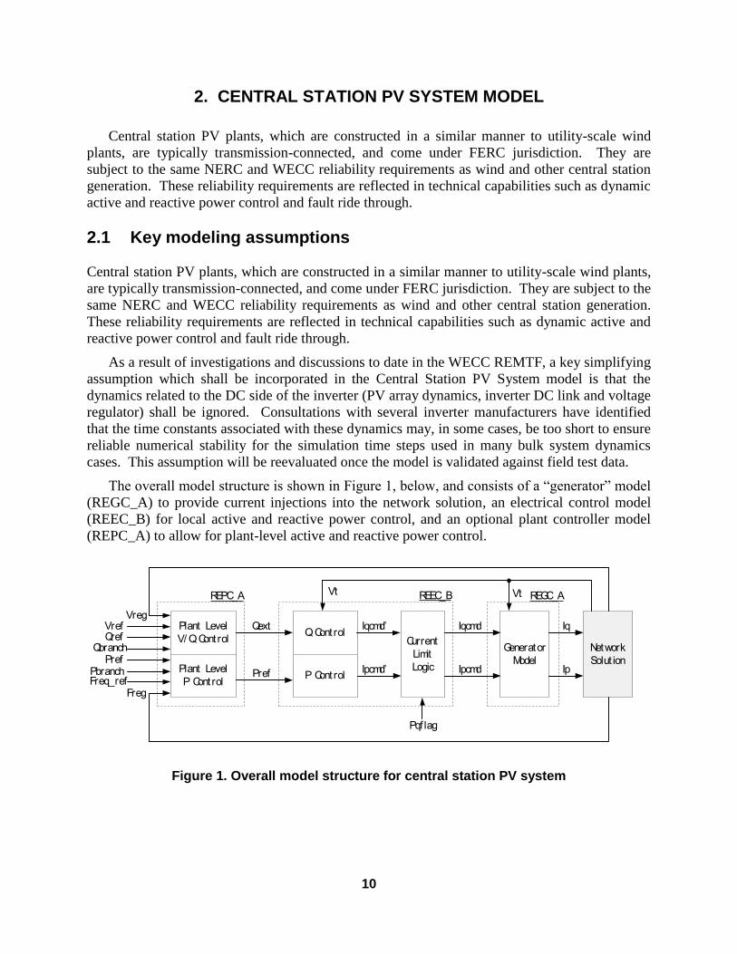
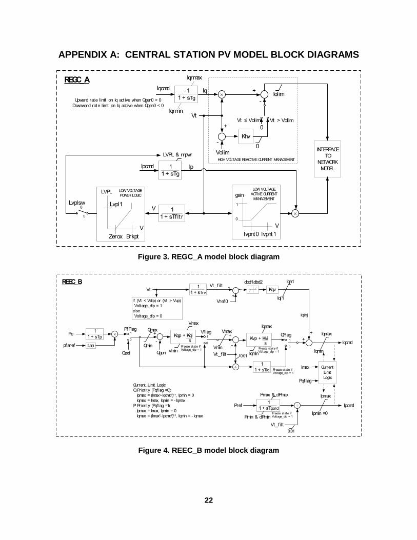
The overall model structure is shown in Figure 1, below, and consists of a “generator” model
(REGC_A) to provide current injections into the network solution, an electrical control model
(REEC_B) for local active and reactive power control, and an optional plant controller model
(REPC_A) to allow for plant-level active and reactive power control.
Q Control
P Control
Current
Limit
Logic
IqcmdIqcmd’
IpcmdIpcmd’
Generator
Model
Network
Solut ion
Plant Level
V/ Q Control
Plant Level
P Control
VrefVreg
QrefQbranch
PrefPbranchFreq_ref
Freg
Qext
Pref
REPC_A
Pqf lag
REEC_B REGC_AVt Vt
Iq
Ip
Figure 1. Overall model structure for central station PV system
11
2.2 Subsystem models
The model shall incorporate a high bandwidth current regulator that injects real and reactive
components of inverter current into the external network during the network solution in response
to real and reactive current commands. Current injection is included in the REGC_A model.
2.2.1 Current injection
Current injection shall include the following capabilities:
• User settable reactive current management during high voltage events at the generator
(inverter) terminal bus
• Active current management during low voltage events to approximate the response of
the inverter PLL controls during voltage dips
• Power logic during low voltage events to allow for a controlled response of active
current during and immediately following voltage dips
• The current injection model is identical to that which the WECC REMTF is
proposing to utilize for the Type 3 and Type 4 generic wind turbine models.
2.2.2 Local active power control
The active power control subsystem included in the REEC_B model shall provide the active
current command to the current injection model. The active current command shall be subject to
current limiting, with user-selectable priority between active and reactive current. The active
current command shall be derived from a reference active power and the inverter terminal
voltage determined in the network solution. The reference active power shall be the initial active
power from the solved power flow case; or, in the case where a plant controller model
(REPC_A) is included, from the plant controller.
2.2.3 Local reactive power control
The reactive power control subsystem included in the REEC_B model shall provide the reactive
current command to the current injection model. The reactive current command shall be subject
to current limiting, with user-selectable priority between active and reactive current. The
following reactive power control modes shall be accommodated:
• Constant power factor, based on the inverter power factor in the solved power flow
case
• Constant reactive power, based either on the inverter absolute reactive power in the
solved power flow case or, in the case where a plant controller model (REPC_A) is
included, from the plant controller.
The option to process the reactive power command via a cascaded set of PI regulators for local
reactive power and terminal voltage control (refer to Figure 4), or to bypass these regulators and
directly derive a reactive current command from the inverter terminal voltage, shall be provided.
12
In addition, a supplementary, fast-acting reactive current response to abnormally high or low
terminal voltages (again, refer to Figure 4) shall be provided.
2.2.4 Protective functions
The protective functions included in the REGC_A model shall incorporate either of the
following:
a) A set of six or more definite time voltage and frequency protective elements used to trip
the generation represented by the model. Each element shall have an independent user-
settable pickup and time delay.
b) The ability to trip the generation represented by the model via external models providing
the same functionality. Examples of such external models include the LHFRT and
LHVRT models currently available in PSLF, and the FRQDCA/FRQTPA and
VTGDCA/VTGTPA models currently available in PSS®E.
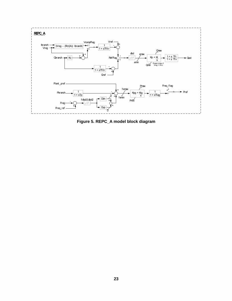
2.2.5 Plant level active and reactive power control
The plant controller model (REPC_A) is an optional model used when plant-level control of
active and/or reactive power is desired. The model shall incorporate the following:
• Closed loop voltage regulation at a user-designated bus. The voltage feedback signal
shall have provisions line drop compensation, voltage droop response and a user-
settable deadband on the voltage error signal.
• Closed loop reactive power regulation on a user-designated branch with a user-
settable deadband on the reactive power error signal.
• A plant-level governor response signal derived from frequency deviation at a user-
designated bus. The frequency droop response shall be applied to active power flow
on a user user-designated branch.
• Frequency droop control shall be capable of being activated in both over and under
frequency conditions. The frequency deviation applied to the droop gain shall be
subject to a user-settable deadband.
The plant controller model is identical to that which the WECC REMTF is proposing to utilize
for the Type 3 and Type 4 generic wind turbine models.
Please see Appendix A for block diagrams for the central station PV subsystem models. The
corresponding input parameter tables are located in Appendix B.
13
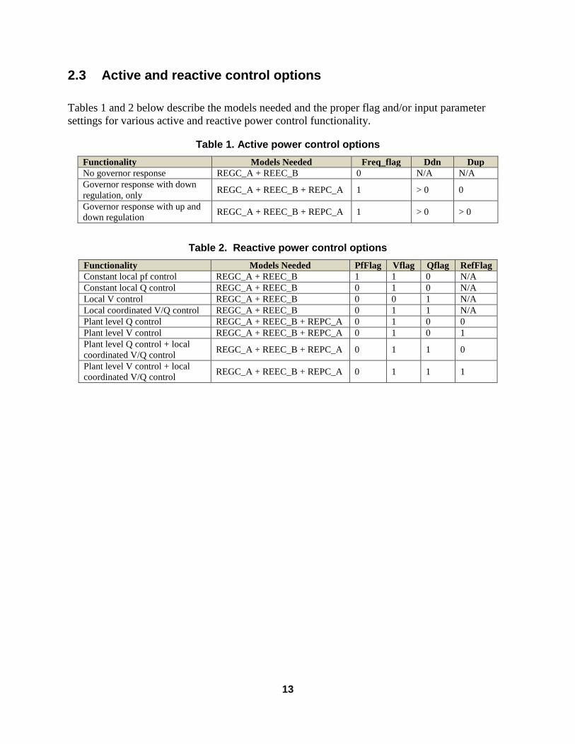
2.3 Active and reactive control options
Tables 1 and 2 below describe the models needed and the proper flag and/or input parameter
settings for various active and reactive power control functionality.
Table 1. Active power control options
Functionality Models Needed Freq_flag Ddn Dup
No governor response REGC_A + REEC_B 0 N/A N/A
Governor response with down
regulation, only REGC_A + REEC_B + REPC_A 1 > 0 0
Governor response with up and
down regulation REGC_A + REEC_B + REPC_A 1 > 0 > 0
Table 2. Reactive power control options
Functionality Models Needed PfFlag Vflag Qflag RefFlag
Constant local pf control REGC_A + REEC_B 1 1 0 N/A
Constant local Q control REGC_A + REEC_B 0 1 0 N/A
Local V control REGC_A + REEC_B 0 0 1 N/A
Local coordinated V/Q control REGC_A + REEC_B 0 1 1 N/A
Plant level Q control REGC_A + REEC_B + REPC_A 0 1 0 0
Plant level V control REGC_A + REEC_B + REPC_A 0 1 0 1
Plant level Q control + local
coordinated V/Q control REGC_A + REEC_B + REPC_A 0 1 1 0
Plant level V control + local
coordinated V/Q control REGC_A + REEC_B + REPC_A 0 1 1 1
14
3. DISTRIBUTED PV SYSTEM MODEL (PVD1)
Unlike central station PV plants, distributed PV systems are connected at the distribution
level, and thus are under state jurisdiction. Reliability and interconnection requirements, while
varying from state to state, tend to reflect the requirements outlined in IEEE Standard 1547. In
contrast with NERC and WECC central station reliability requirements, distributed PV systems
at this time normally do not participate in steady state voltage regulation, and tighter bounds on
operation for off-nominal voltage and frequency conditions result in significantly different fault
ride-through capability.
3.1 Key modeling assumptions
In the near term, it is anticipated that the PV inverters applied in distributed systems will
continue to comply with IEEE 1547, and will operate under constant power factor or constant
reactive power modes of operation. The elimination of the closed-loop voltage regulator
dynamics, along with the elimination of the DC dynamics (for the same reasons described for the
Central Station model), allows for substantial simplification of the model with respect to that of
the Central Station. However, unlike a Central Station plant, the terminal voltages seen by the
individual inverters within the composite load in the bulk system dynamic model are likely to
vary substantially. A different protection model is used to capture the effect of the diverse
terminal conditions on the aggregate generation.
Note: The REMTF is currently considering the possibility of integrating this model into the
existing WECC complex load model (CMPLDW). However, the integration of this model into
CMPLDW is outside the scope of this document.
3.2 Control and protective functions
3.2.1 Active power control
The active power control subsystem shall provide the active current injection to the network
solution. The active current command shall be subject to current limiting, with user-selectable
priority between active and reactive current. The active current command shall be derived from
a reference active power and the inverter terminal voltage determined in the network solution.
The reference active power shall be the initial active power from the solved power flow case.
The active power control subsystem shall provide a high frequency droop (governor response)
function with user-settable deadband and droop gain.
15
3.2.2 Reactive power control
The reactive power control subsystem shall provide the reactive current command to the network
solution. The reactive current command shall be subject to apparent current limiting, with user-
selectable priority between active and reactive current. The reactive power control mode shall be
limited to constant reactive power. The reference reactive power shall be the sum of the
following:
• The initial reactive power from the solved power flow case
• A droop signal derived from voltage deviation at a user-specified bus.
• The voltage deviation applied to the droop characteristic shall be subject to deadband
control and line drop compensation.
3.2.3 Protective functions
The model shall incorporate functions which reduce generation outside of user-specified
deadbands on voltage and frequency in an amount proportional to the voltage or frequency
deviation. User-settable flags shall determine whether recovery of generation shall occur when
voltage or frequency excursions reverse and return toward the deadband, and in what proportion.
The tripping logic shall be as follows:
For low-voltage tripping:
if( Vt < Vmin ) Vmin = Vt # Initially, Vmin = Vt or a large value
if( Vmin < Vt0 ) Vmin = Vt0 # Vmin tracks the lowest voltage
if( Vt < Vt0 )
Fvl = 0.0 # All generation is tripped below Vt0
else if( Vt < Vt1 )
if( Vt <= Vmin )
Fvl = (Vmin – Vt0) / (Vt1 – Vt0)
else
Fvl = ((Vmin – Vt0) + Vrflag * (Vt - Vmin)) / (Vt1 – Vt0)
endif
else
if( Vmin >= Vt1 )
Fvl = 1.0 # If Vt has not gone below Vt1
else # Vt fell below Vt1 but recovered
Fvl = ((vmin – Vt0) + Vrflag * (Vt1 - vmin)) / (Vt1 – Vt0)
endif
endif
The logic for high-voltage tripping is presented below.
16
For high-voltage tripping:
if( Vt > Vmax ) Vmax = Vt # Initially, Vmax = Vt or 0
if( Vmax > Vt3 ) Vmax = Vt3
if( Vt > Vt3 )
Fvh = 0.0
else if( Vt > Vt2 )
if( Vt >= Vmax )
Fvh = (Vt3 - Vmax) / (Vt3 – Vt2)
else
Fvh = ((Vt3 - Vmax) + Vrflag * (Vmax - Vt)) / (Vt3 – Vt2)
endif
else
if( Vmax <= Vt2 )
Fvh = 1.0
else
Fvh = ((Vt3 - Vmax) + Vrflag * (Vmax – Vt2)) / (Vt3 – Vt2)
endif
endif
The logic for the low and high frequency tripping is the same with “V” replaced by “F”. The
outputs of this logic are four factors (Fvl, Fvh, Ffl and Ffh) which represent the “untripped” PV
generation on a per unit basis. The multiplication of these factors, in the manner shown in
Figure 2, results in a reduction in aggregate active and reactive current under the assumption that
voltage and frequency tripping events following a disturbance are statistically uncorrelated.
3.3 Model block diagram
÷
Vt
N
D
×
Q Priority (Pqf lag =0)
Iqmax = Imax
Iqmin = - Iqmax
Ipmax = (Imax2- Iqcmd2)1/ 2
P Priority (Pqf lag =1)
Ipmax = Imax
Iqmax = (Imax2- Ipcmd2)1/ 2
Iqmin = - Iqmax
÷
0
Ipmax
Iqmin
Iqmax
0.01
N
D
×
Vt0 Vt1 Vt2 Vt3
1
0
V0 V1
DqdvQmx
Qmn
Qref
vrrecov
Freq
Ft0 Ft1 Ft2 Ft3
1
0
f rrecov
Ip
Iq
It = Ip +j Iq
-1
1 + sTg
1
1 + sTg
Ipcmd
Iqcmd
PVD1
XcIt
Qref
-
Freq_ref Ddn
fdbd
Pdrp
Pref
Pext
Pdrp
Fvl
Ffh
Ff l
Fvh
Fvl
Ffh
Ff l
Fvh
×
+
+ +
+
++
+
+
Figure 2. Distributed PV model block diagram

17
18
4. CONCLUDING REMARKS
This document was written to serve as a specification for generic solar photovoltaic (PV) system
positive-sequence dynamic models for use in time-domain simulations of the bulk power system
in accordance with NERC MOD standards. Two specific dynamic models were discussed in this
document. The first, a Central Station PV System model, was designed to capture the most
important dynamic characteristics of large scale PV systems with a central Point of
Interconnection (POI) at the transmission level. The second, a Distributed PV System model,
was designed to represent an aggregation of smaller, distribution-connected systems that
comprise a portion of a composite load that might be modeled at a transmission load bus.

19
20
5. REFERENCES
1. W.W. Price. “CMPLDWG - Composite Load Model with Photovoltaic Distributed
Generation.” WECC document, July 2012.

21
22
APPENDIX A: CENTRAL STATION PV MODEL BLOCK DIAGRAMS
REGC_A
Ipcmd 1
1 + sTg
LVPL & rrpwr
lvpnt0 lvpnt1
gain
V
1
0×
Ip
INTERFACE
TO
NETWORK
MODEL
LOW VOLTAGE
ACTIVE CURRENT
MANAGEMENT
Iqcmd -1
1 + sTg
Iq×
Volim
-Khv
0
0
Vt ≤ Volim Vt > Volim
HIGH VOLTAGE REACTIVE CURRENT MANAGEMENT
Iolim
Vt
-
V
Zerox Brkpt
Lvpl1
LVPL
V
LOW VOLTAGE
POWER LOGIC
0
1
Lvplsw1
1 + sTf lt r
Iqrmin
Iqrmax
+
+
Upward rate limit on Iq act ive when Qgen0 > 0
Downward rate limit on Iq act ive when Qgen0 < 0
Figure 3. REGC_A model block diagram
Current Limit Logic
Q Priority (Pqf lag =0):
Ipmax = (Imax2- Iqcmd2)1/ 2, Ipmin = 0
Iqmax = Imax, Iqmin = - Iqmax
P Priority (Pqf lag =1):
Ipmax = Imax, Ipmin = 0
Iqmax = (Imax2- Ipcmd2)1/ 2, Iqmin = - Iqmax
÷ Ipcmd1
1 + sTpord
Pmax & dPmax
Pmin & dPmin
Iqcmd
÷
Iqmax
Iqmin
Iqh1
Iql1
Kqv
dbd1,dbd2
Vref0
Vt-
iqinj
REEC_B
pfaref
×
tan Qmin
Qmax1
1 + sTpPe 1
0
PfFlag
Qext Qgen
-
Kqp + Kqi s
Vmax
Freeze state if Voltage_dip = 1Vmin
1
0
Vmin
Vf lag VmaxIqmax
Kvp + Kvi s
Freeze state if Voltage_dip = 1
Iqmin
1
1 + sTrv
Vt_f ilt
if (Vt < Vdip) or (Vt > Vup)
Voltage_dip = 1
else
Voltage_dip = 0
Current
Limit
Logic
1
0
QFlag
-
Vt_f ilt 0.01
1
1 + sTiq Freeze state if Voltage_dip = 1
Vt_f ilt
0.01
Ipmax
Ipmin =0
Imax
Pqf lag
Freeze state if Voltage_dip = 1
Pref
+
+
++
+
Figure 4. REEC_B model block diagram
23
REPC_A
1
0
Vreg
Vref
Freeze state if Vreg < Vfrz
Ibranch
Kc
-
Qbranch
emax
emin
Kp + Ki s
Qmax
Qmin
1 + s Tf t1 + s Tfv
QextRefFlag
dbd
1
1 + sTf lt r
VcompFlag
|Vreg – (Rc+jXc)· Ibranch|
1
1 + sTf lt r
1
0
Qref
-
femin
femax
Pbranch
Plant_pref
Ddn
Dup
0
0Freq_ref
-fdbd1,fdbd2
- Kpg + Kig s
Pmax
PminFreg
1
1 + sTp
1
1 + sTlagPref
++
+
+
+
+
+
+
+ 0
1
Freq_f lag
Figure 5. REPC_A model block diagram
24
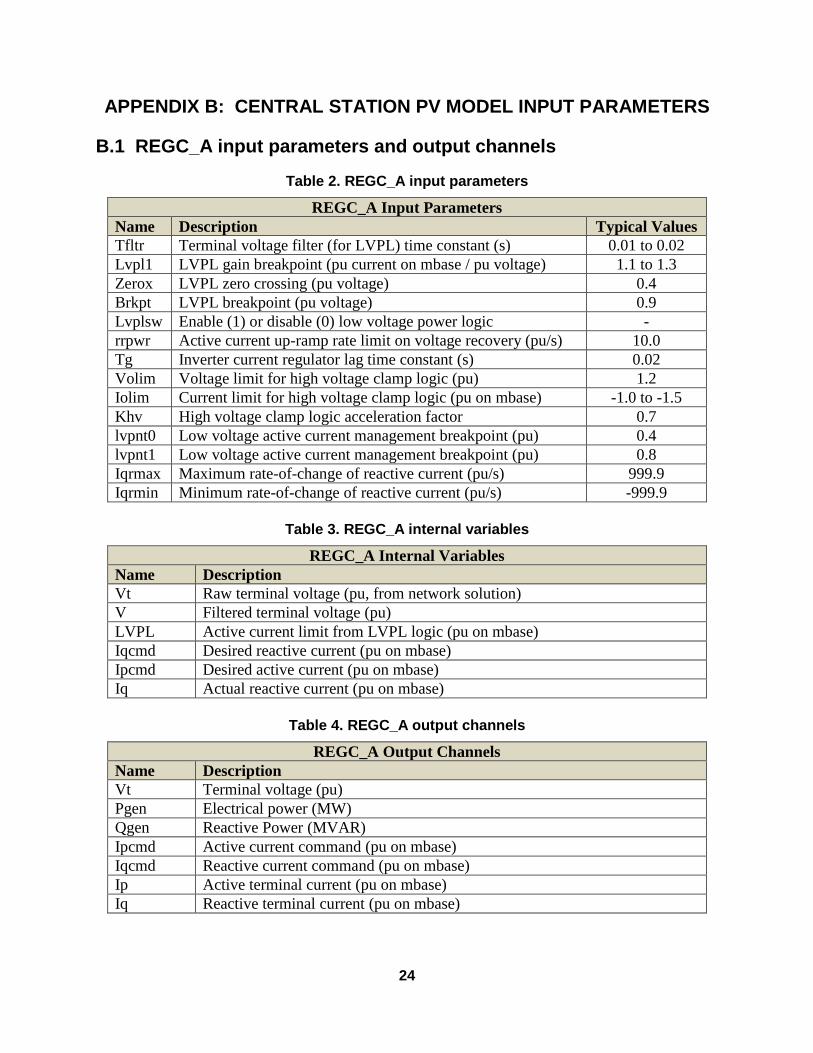
APPENDIX B: CENTRAL STATION PV MODEL INPUT PARAMETERS
B.1 REGC_A input parameters and output channels
Table 2. REGC_A input parameters
REGC_A Input Parameters
Name Description Typical Values
Tfltr Terminal voltage filter (for LVPL) time constant (s) 0.01 to 0.02
Lvpl1 LVPL gain breakpoint (pu current on mbase / pu voltage) 1.1 to 1.3
Zerox LVPL zero crossing (pu voltage) 0.4
Brkpt LVPL breakpoint (pu voltage) 0.9
Lvplsw Enable (1) or disable (0) low voltage power logic -
rrpwr Active current up-ramp rate limit on voltage recovery (pu/s) 10.0
Tg Inverter current regulator lag time constant (s) 0.02
Volim Voltage limit for high voltage clamp logic (pu) 1.2
Iolim Current limit for high voltage clamp logic (pu on mbase) -1.0 to -1.5
Khv High voltage clamp logic acceleration factor 0.7
lvpnt0 Low voltage active current management breakpoint (pu) 0.4
lvpnt1 Low voltage active current management breakpoint (pu) 0.8
Iqrmax Maximum rate-of-change of reactive current (pu/s) 999.9
Iqrmin Minimum rate-of-change of reactive current (pu/s) -999.9
Table 3. REGC_A internal variables
REGC_A Internal Variables
Name Description
Vt Raw terminal voltage (pu, from network solution)
V Filtered terminal voltage (pu)
LVPL Active current limit from LVPL logic (pu on mbase)
Iqcmd Desired reactive current (pu on mbase)
Ipcmd Desired active current (pu on mbase)
Iq Actual reactive current (pu on mbase)
Table 4. REGC_A output channels
REGC_A Output Channels
Name Description
Vt Terminal voltage (pu)
Pgen Electrical power (MW)
Qgen Reactive Power (MVAR)
Ipcmd Active current command (pu on mbase)
Iqcmd Reactive current command (pu on mbase)
Ip Active terminal current (pu on mbase)
Iq Reactive terminal current (pu on mbase)
25
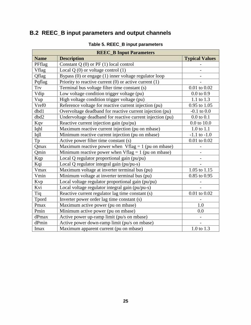
B.2 REEC_B input parameters and output channels
Table 5. REEC_B input parameters
REEC_B Input Parameters
Name Description Typical Values
PFflag Constant Q (0) or PF (1) local control -
Vflag Local Q (0) or voltage control (1) -
Qflag Bypass (0) or engage (1) inner voltage regulator loop -
Pqflag Priority to reactive current (0) or active current (1) -
Trv Terminal bus voltage filter time constant (s) 0.01 to 0.02
Vdip Low voltage condition trigger voltage (pu) 0.0 to 0.9
Vup High voltage condition trigger voltage (pu) 1.1 to 1.3
Vref0 Reference voltage for reactive current injection (pu) 0.95 to 1.05
dbd1 Overvoltage deadband for reactive current injection (pu) -0.1 to 0.0
dbd2 Undervoltage deadband for reactive current injection (pu) 0.0 to 0.1
Kqv Reactive current injection gain (pu/pu) 0.0 to 10.0
Iqhl Maximum reactive current injection (pu on mbase) 1.0 to 1.1
Iqll Minimum reactive current injection (pu on mbase) -1.1 to -1.0
Tp Active power filter time constant (s) 0.01 to 0.02
Qmax Maximum reactive power when Vflag = 1 (pu on mbase) -
Qmin Minimum reactive power when Vflag = 1 (pu on mbase) -
Kqp Local Q regulator proportional gain (pu/pu) -
Kqi Local Q regulator integral gain (pu/pu-s) -
Vmax Maximum voltage at inverter terminal bus (pu) 1.05 to 1.15
Vmin Minimum voltage at inverter terminal bus (pu) 0.85 to 0.95
Kvp Local voltage regulator proportional gain (pu/pu) -
Kvi Local voltage regulator integral gain (pu/pu-s) -
Tiq Reactive current regulator lag time constant (s) 0.01 to 0.02
Tpord Inverter power order lag time constant (s) -
Pmax Maximum active power (pu on mbase) 1.0
Pmin Minimum active power (pu on mbase) 0.0
dPmax Active power up-ramp limit (pu/s on mbase) -
dPmin Active power down-ramp limit (pu/s on mbase) -
Imax Maximum apparent current (pu on mbase) 1.0 to 1.3
26
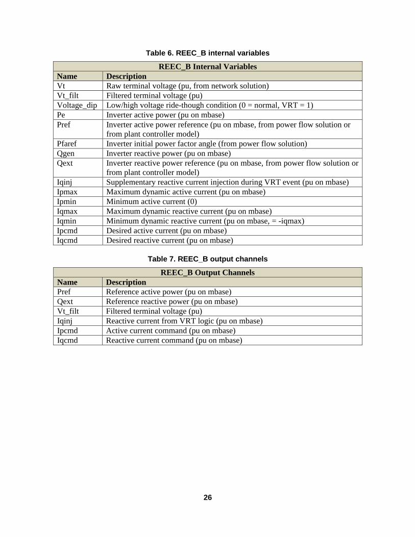
Table 6. REEC_B internal variables
REEC_B Internal Variables
Name Description
Vt Raw terminal voltage (pu, from network solution)
Vt_filt Filtered terminal voltage (pu)
Voltage_dip Low/high voltage ride-though condition (0 = normal, VRT = 1)
Pe Inverter active power (pu on mbase)
Pref Inverter active power reference (pu on mbase, from power flow solution or
from plant controller model)
Pfaref Inverter initial power factor angle (from power flow solution)
Qgen Inverter reactive power (pu on mbase)
Qext Inverter reactive power reference (pu on mbase, from power flow solution or
from plant controller model)
Iqinj Supplementary reactive current injection during VRT event (pu on mbase)
Ipmax Maximum dynamic active current (pu on mbase)
Ipmin Minimum active current (0)
Iqmax Maximum dynamic reactive current (pu on mbase)
Iqmin Minimum dynamic reactive current (pu on mbase, = -iqmax)
Ipcmd Desired active current (pu on mbase)
Iqcmd Desired reactive current (pu on mbase)
Table 7. REEC_B output channels
REEC_B Output Channels
Name Description
Pref Reference active power (pu on mbase)
Qext Reference reactive power (pu on mbase)
Vt_filt Filtered terminal voltage (pu)
Iqinj Reactive current from VRT logic (pu on mbase)
Ipcmd Active current command (pu on mbase)
Iqcmd Reactive current command (pu on mbase)
27
B.3 REPC_A input parameters and output channels
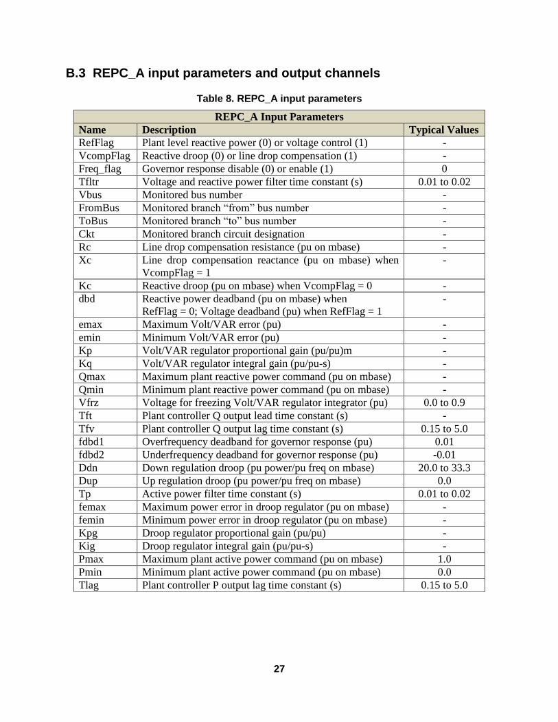
Table 8. REPC_A input parameters
REPC_A Input Parameters
Name Description Typical Values
RefFlag Plant level reactive power (0) or voltage control (1) -
VcompFlag Reactive droop (0) or line drop compensation (1) -
Freq_flag Governor response disable (0) or enable (1) 0
Tfltr Voltage and reactive power filter time constant (s) 0.01 to 0.02
Vbus Monitored bus number -
FromBus Monitored branch “from” bus number -
ToBus Monitored branch “to” bus number -
Ckt Monitored branch circuit designation -
Rc Line drop compensation resistance (pu on mbase) -
Xc Line drop compensation reactance (pu on mbase) when
VcompFlag = 1
-
Kc Reactive droop (pu on mbase) when VcompFlag = 0 -
dbd Reactive power deadband (pu on mbase) when
RefFlag = 0; Voltage deadband (pu) when RefFlag = 1
-
emax Maximum Volt/VAR error (pu) -
emin Minimum Volt/VAR error (pu) -
Kp Volt/VAR regulator proportional gain (pu/pu)m -
Kq Volt/VAR regulator integral gain (pu/pu-s) -
Qmax Maximum plant reactive power command (pu on mbase) -
Qmin Minimum plant reactive power command (pu on mbase) -
Vfrz Voltage for freezing Volt/VAR regulator integrator (pu) 0.0 to 0.9
Tft Plant controller Q output lead time constant (s) -
Tfv Plant controller Q output lag time constant (s) 0.15 to 5.0
fdbd1 Overfrequency deadband for governor response (pu) 0.01
fdbd2 Underfrequency deadband for governor response (pu) -0.01
Ddn Down regulation droop (pu power/pu freq on mbase) 20.0 to 33.3
Dup Up regulation droop (pu power/pu freq on mbase) 0.0
Tp Active power filter time constant (s) 0.01 to 0.02
femax Maximum power error in droop regulator (pu on mbase) -
femin Minimum power error in droop regulator (pu on mbase) -
Kpg Droop regulator proportional gain (pu/pu) -
Kig Droop regulator integral gain (pu/pu-s) -
Pmax Maximum plant active power command (pu on mbase) 1.0
Pmin Minimum plant active power command (pu on mbase) 0.0
Tlag Plant controller P output lag time constant (s) 0.15 to 5.0
28
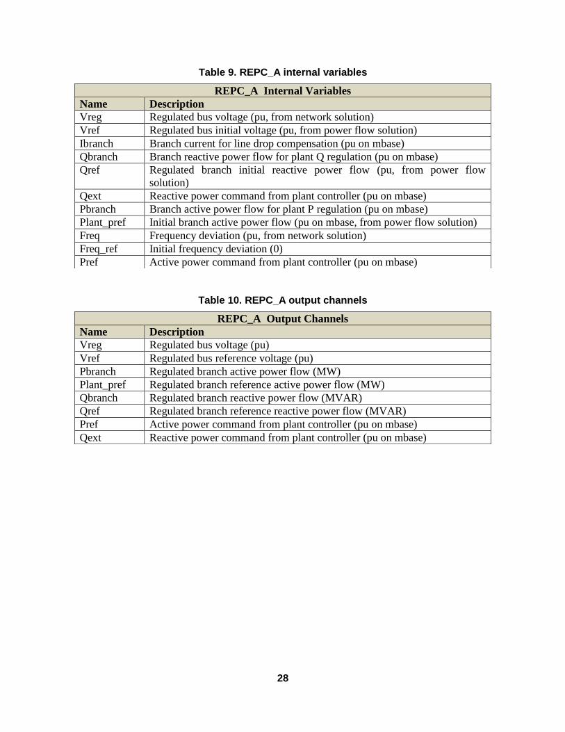
Table 9. REPC_A internal variables
Table 10. REPC_A output channels
REPC_A Internal Variables
Name Description
Vreg Regulated bus voltage (pu, from network solution)
Vref Regulated bus initial voltage (pu, from power flow solution)
Ibranch Branch current for line drop compensation (pu on mbase)
Qbranch Branch reactive power flow for plant Q regulation (pu on mbase)
Qref Regulated branch initial reactive power flow (pu, from power flow
solution)
Qext Reactive power command from plant controller (pu on mbase)
Pbranch Branch active power flow for plant P regulation (pu on mbase)
Plant_pref Initial branch active power flow (pu on mbase, from power flow solution)
Freq Frequency deviation (pu, from network solution)
Freq_ref Initial frequency deviation (0)
Pref Active power command from plant controller (pu on mbase)
REPC_A Output Channels
Name Description
Vreg Regulated bus voltage (pu)
Vref Regulated bus reference voltage (pu)
Pbranch Regulated branch active power flow (MW)
Plant_pref Regulated branch reference active power flow (MW)
Qbranch Regulated branch reactive power flow (MVAR)
Qref Regulated branch reference reactive power flow (MVAR)
Pref Active power command from plant controller (pu on mbase)
Qext Reactive power command from plant controller (pu on mbase)
29
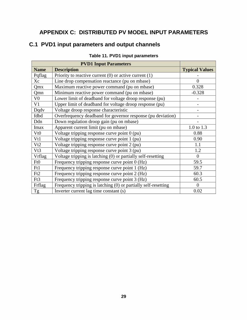
APPENDIX C: DISTRIBUTED PV MODEL INPUT PARAMETERS
C.1 PVD1 input parameters and output channels
Table 11. PVD1 input parameters
PVD1 Input Parameters
Name Description Typical Values
Pqflag Priority to reactive current (0) or active current (1) -
Xc Line drop compensation reactance (pu on mbase) 0
Qmx Maximum reactive power command (pu on mbase) 0.328
Qmn Minimum reactive power command (pu on mbase) -0.328
V0 Lower limit of deadband for voltage droop response (pu) -
V1 Upper limit of deadband for voltage droop response (pu) -
Dqdv Voltage droop response characteristic -
fdbd Overfrequency deadband for governor response (pu deviation) -
Ddn Down regulation droop gain (pu on mbase) -
Imax Apparent current limit (pu on mbase) 1.0 to 1.3
Vt0 Voltage tripping response curve point 0 (pu) 0.88
Vt1 Voltage tripping response curve point 1 (pu) 0.90
Vt2 Voltage tripping response curve point 2 (pu) 1.1
Vt3 Voltage tripping response curve point 3 (pu) 1.2
Vrflag Voltage tripping is latching (0) or partially self-resetting 0
Ft0 Frequency tripping response curve point 0 (Hz) 59.5
Ft1 Frequency tripping response curve point 1 (Hz) 59.7
Ft2 Frequency tripping response curve point 2 (Hz) 60.3
Ft3 Frequency tripping response curve point 3 (Hz) 60.5
Frflag Frequency tripping is latching (0) or partially self-resetting 0
Tg Inverter current lag time constant (s) 0.02
30
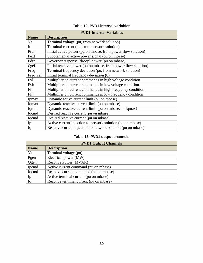
Table 12. PVD1 internal variables
PVD1 Internal Variables
Name Description
Vt Terminal voltage (pu, from network solution)
It Terminal current (pu, from network solution)
Pref Initial active power (pu on mbase, from power flow solution)
Pext Supplemental active power signal (pu on mbase)
Pdrp Governor response (droop) power (pu on mbase)
Qref Initial reactive power (pu on mbase, from power flow solution)
Freq Terminal frequency deviation (pu, from network solution)
Freq_ref Initial terminal frequency deviation (0)
Fvl Multiplier on current commands in high voltage condition
Fvh Multiplier on current commands in low voltage condition
Ffl Multiplier on current commands in high frequency condition
Ffh Multiplier on current commands in low frequency condition
Ipmax Dynamic active current limit (pu on mbase)
Iqmax Dynamic reactive current limit (pu on mbase)
Iqmin Dynamic reactive current limit (pu on mbase, = -Iqmax)
Iqcmd Desired reactive current (pu on mbase)
Iqcmd Desired reactive current (pu on mbase)
Ip Active current injection to network solution (pu on mbase)
Iq Reactive current injection to network solution (pu on mbase)
Table 13. PVD1 output channels
PVD1 Output Channels
Name Description
Vt Terminal voltage (pu)
Pgen Electrical power (MW)
Qgen Reactive Power (MVAR)
Ipcmd Active current command (pu on mbase)
Iqcmd Reactive current command (pu on mbase)
Ip Active terminal current (pu on mbase)
Iq Reactive terminal current (pu on mbase)

31
DISTRIBUTION
1 MS0899 Technical Library 9536 (electronic copy)

32