
Generic Closed Loop Controller for Power Regulation in ...
10
Abstract— This paper presents a comprehensive and generalized analysis of the bidirectional dual active bridge (DAB) DC/DC converter using triple phase shift (TPS) control to enable closed loop power regulation while minimizing current stress. The key new achievements are: a generic analysis in terms of possible conversion ratios/converter voltage gains (i.e. Buck/Boost/Unity), per unit based equations regardless of DAB ratings, and a new simple closed loop controller implementable in real time to meet desired power transfer regulation at minimum current stress. Per unit based analytical expressions are derived for converter AC RMS current as well as power transferred. An offline particle swarm optimization (PSO) method is used to obtain an extensive set of TPS ratios for minimizing the RMS current in the entire bidirectional power range of -1 to 1 per unit. The extensive set of results achieved from PSO presents a generic data pool which is carefully analyzed to derive simple useful relations. Such relations enabled a generic closed loop controller design that can be implemented in real time avoiding the extensive computational capacity that iterative optimization techniques require. A detailed Simulink DAB switching model is used to validate precision of the proposed closed loop controller under various operating conditions. An experimental prototype also substantiates the results achieved. Index Terms— Current stress, Dual active bridge (DAB), Particle swarm optimization (PSO), Triple phase shift (TPS). I. INTRODUCTION UAL active bridge (DAB), originally proposed in the 1990s [1], significantly attracted researchers among several bidirectional DC/DC converters [2] such as dual- flyback, dual-Cuk, Zeta-Sepic, forward-flyback, dual-push- pull, push-pull-forward, push-pull-flyback and dual-half- bridge. This is mainly due to its high power handing capability, zero voltage switching (ZVS) characteristics, high power density, galvanic isolation in transformer based versions and the possibility of cascaded or modular configuration to enable higher power/higher voltage designs [3-7]. Due to these advantages, DAB DC/DC converters have attracted more attention in power energy conversion applications, such as dc microgrids, medium voltage dc (MVDC) and high voltage dc (HVDC) transmission systems [8-10]. In addition, DAB DC/DC converters have been widely used in distributed generating systems incorporating variable-nature energy resources, such as PV or wind, for voltage matching/stepping and accommodating power regulation between energy storage systems, energy sources and load demands [11-14]. Studies have been on going to analyze, control and improve the overall performance of the DAB converter. Phase shift control techniques are the most common modulation schemes in literature due to their implementation simplicity, fundamental frequency operation which reduces switching losses, uniform conduction of switching devices, enabling of ZVS operation and non-active power circulation control within converter [2, 3, 14]. The conventional phase shift (CPS), or single phase shift (SPS), was the first proposed technique [1] where the phase shift angle between the two active bridges controls the power flow. Then, dual phase shift (DPS) modulation technique was introduced in [15] by adding the same inner phase shift to the bridge voltages to overcome the phenomenon of backflow power that appeared when using CPS. Extended phase shift (EPS) was proposed [16] in order to extend the ZVS range of the DAB converter, by controlling the duty cycle of one of the bridge voltages. The above mentioned modulation techniques (SPS, DPS and EPS) share a common drawback which is not exploiting all possible control variables which results in reduced efficiency of DAB operation. In this regard, Triple phase shift (TPS) [17-19] introduces an additional control variable which can lead to further improvement of ZVS range and reducing the overall losses hence increasing the efficiency. TPS control utilizes the phase shift angle between the bridges in addition to inner phase shifts at both bridges separately which makes TPS the most general modulation control (three degrees of freedom) [20]. A full performance analysis of DAB under TPS control as well as detailed analytical derivations and operational constraints for all possible switching modes were presented in [20, 21] where the voltage conversion is not included in the proposed model which is a major drawback. Considering the aforementioned literature, generalized per unit TPS-based DAB model including the converter voltage conversion ratio is overlooked. Currently, there is a strong trend toward improving the DAB DC/DC converter efficiency while maintaining the power transfer flow control. Different technical aspects can be considered for minimizing overall DAB losses such as non- active power losses [22, 23] and current stresses [16,18,24, 25]. Non-active power loss minimization was tackled in [22] for DAB where the inductor current was analyzed to obtain an operating range where phase shifts achieving minimum non- active power loss can be realized for light and heavy loads in boost operation. However the model was based on the extended phase shift (EPS) modulation technique which result in local optimal operating points at light loads. An iterative algorithm has been proposed in [23] to search for TPS control variables that satisfy the desired active power flow while achieving minimum reactive power consumption. The proposed controller works in an open loop approach with no feedback informing whether actual desired power level is achieved or not. In Generic Closed Loop Controller for Power Regulation in Dual Active Bridge DC/DC Converter with Current Stress Minimization O. Hebala, A.A. Aboushady, K.H. Ahmed, I. Abdelsalam D
Transcript of Generic Closed Loop Controller for Power Regulation in ...

Abstract— This paper presents a comprehensive and
generalized analysis of the bidirectional dual active bridge (DAB)
DC/DC converter using triple phase shift (TPS) control to enable
closed loop power regulation while minimizing current stress. The
key new achievements are: a generic analysis in terms of possible
conversion ratios/converter voltage gains (i.e. Buck/Boost/Unity),
per unit based equations regardless of DAB ratings, and a new
simple closed loop controller implementable in real time to meet
desired power transfer regulation at minimum current stress. Per
unit based analytical expressions are derived for converter AC
RMS current as well as power transferred. An offline particle
swarm optimization (PSO) method is used to obtain an extensive
set of TPS ratios for minimizing the RMS current in the entire
bidirectional power range of -1 to 1 per unit. The extensive set of
results achieved from PSO presents a generic data pool which is
carefully analyzed to derive simple useful relations. Such relations
enabled a generic closed loop controller design that can be
implemented in real time avoiding the extensive computational
capacity that iterative optimization techniques require. A detailed
Simulink DAB switching model is used to validate precision of the
proposed closed loop controller under various operating
conditions. An experimental prototype also substantiates the
results achieved.
Index Terms— Current stress, Dual active bridge (DAB), Particle
swarm optimization (PSO), Triple phase shift (TPS).
I. INTRODUCTION
UAL active bridge (DAB), originally proposed in the
1990s [1], significantly attracted researchers among
several bidirectional DC/DC converters [2] such as dual-
flyback, dual-Cuk, Zeta-Sepic, forward-flyback, dual-push-
pull, push-pull-forward, push-pull-flyback and dual-half-
bridge. This is mainly due to its high power handing capability,
zero voltage switching (ZVS) characteristics, high power
density, galvanic isolation in transformer based versions and the
possibility of cascaded or modular configuration to enable
higher power/higher voltage designs [3-7]. Due to these
advantages, DAB DC/DC converters have attracted more
attention in power energy conversion applications, such as dc
microgrids, medium voltage dc (MVDC) and high voltage dc
(HVDC) transmission systems [8-10]. In addition, DAB
DC/DC converters have been widely used in distributed
generating systems incorporating variable-nature energy
resources, such as PV or wind, for voltage matching/stepping
and accommodating power regulation between energy storage
systems, energy sources and load demands [11-14].
Studies have been on going to analyze, control and improve the
overall performance of the DAB converter. Phase shift control
techniques are the most common modulation schemes in
literature due to their implementation simplicity, fundamental
frequency operation which reduces switching losses, uniform
conduction of switching devices, enabling of ZVS operation
and non-active power circulation control within converter [2, 3,
14]. The conventional phase shift (CPS), or single phase shift
(SPS), was the first proposed technique [1] where the phase shift
angle between the two active bridges controls the power flow.
Then, dual phase shift (DPS) modulation technique was
introduced in [15] by adding the same inner phase shift to the
bridge voltages to overcome the phenomenon of backflow
power that appeared when using CPS. Extended phase shift
(EPS) was proposed [16] in order to extend the ZVS range of
the DAB converter, by controlling the duty cycle of one of the
bridge voltages. The above mentioned modulation techniques
(SPS, DPS and EPS) share a common drawback which is not
exploiting all possible control variables which results in reduced
efficiency of DAB operation. In this regard, Triple phase shift
(TPS) [17-19] introduces an additional control variable which
can lead to further improvement of ZVS range and reducing the
overall losses hence increasing the efficiency. TPS control
utilizes the phase shift angle between the bridges in addition to
inner phase shifts at both bridges separately which makes TPS
the most general modulation control (three degrees of freedom)
[20]. A full performance analysis of DAB under TPS control as
well as detailed analytical derivations and operational
constraints for all possible switching modes were presented in
[20, 21] where the voltage conversion is not included in the
proposed model which is a major drawback. Considering the
aforementioned literature, generalized per unit TPS-based DAB
model including the converter voltage conversion ratio is
overlooked.
Currently, there is a strong trend toward improving the DAB
DC/DC converter efficiency while maintaining the power
transfer flow control. Different technical aspects can be
considered for minimizing overall DAB losses such as non-
active power losses [22, 23] and current stresses [16,18,24, 25].
Non-active power loss minimization was tackled in [22] for
DAB where the inductor current was analyzed to obtain an
operating range where phase shifts achieving minimum non-
active power loss can be realized for light and heavy loads in
boost operation. However the model was based on the extended
phase shift (EPS) modulation technique which result in local
optimal operating points at light loads. An iterative algorithm
has been proposed in [23] to search for TPS control variables
that satisfy the desired active power flow while achieving
minimum reactive power consumption. The proposed controller
works in an open loop approach with no feedback informing
whether actual desired power level is achieved or not. In
Generic Closed Loop Controller for Power
Regulation in Dual Active Bridge DC/DC
Converter with Current Stress Minimization O. Hebala, A.A. Aboushady, K.H. Ahmed, I. Abdelsalam
D
addition, the method is not generalized for buck and boost DAB
operating modes. Authors in [24] used Lagrange Multiplier
method to calculate the optimal phase shift ratios for any given
power level targeting minimum current stresses defined as RMS
inductor current. However, the three proposed converter
switching modes do not cover the entire bidirectional power
range but only cover operation from -0.5 to 1 pu, therefore the
proposed scheme cannot be considered universal. An analytical
method based on Karush-Kahn-Tucker method was developed
in [18] to get the global optimal control parameters achieving
minimum RMS current stresses for DAB under a modified TPS
control where the outer phase shift between the fundamental
components of bridges voltage is introduced. However, the
analysis is based on fundamental frequency analysis where the
square bridge voltages of the DAB are replaced by the
fundamental frequency components. This ignores the effect of
higher order harmonics on effective increase of RMS current.
In other cases, the researchers focused on minimizing the per
unit peak current in [16] and [25]. Considering the
aforementioned literature, RMS inductor current can be
considered to be the most effective amongst other minimization
objectives such as non-active power loss, peak or average
inductor current. This is due to the fact that RMS current
stresses have a direct impact on the conduction losses which are
considered to be the dominant portion of losses [26, 27]. In
addition, conduction and copper losses are proportional to the
square of the RMS current [28]. Now, it is a quite clear from literature that the shortcomings in
previous DAB current optimization researches can be
summarized as follows: non-generalized per unit analysis,
discarding the effect of converter voltage gain with bidirectional
power flow, cumbersome analysis in some cases, achieving
local minimal solutions in some cases due to restricting
optimization to a specific control technique or load range and
finally impracticality of some derived controllers for real time
implementation. It is obvious that no work has completely
tackled all challenges simultaneously and most importantly
without compromising on level of control complexity and
implementing optimization in real time. This paper has
identified this research gap therefore proposing an all-round
universal solution to the mentioned shortcomings.
The paper comprises 7 sections. Section 2 covers the
generalized per unit DAB model under TPS control. Sections 3
and 4 present the offline optimization process that was carried
out by applying PSO to the derived per unit DAB model to
obtain the global optimal phase shift ratios for minimizing RMS
current at full power range for different converter voltage gains.
The outcome from the optimization process is a generalized
relation between desired power transfer and the optimal phase
ratios as a function of the voltage conversion ratio. This
generalized relation is used for designing a novel simple closed
loop controller which is discussed in detail in section 5.
Afterwards, Simulation results using the proposed closed loop
controller are presented in section 6. Finally, section 7 presents
a low scaled experimental prototype which confirms the
simulation results.
II. GENERALIZED PER UNIT ANALYSIS OF DAB UNDER TPS
CONTROL
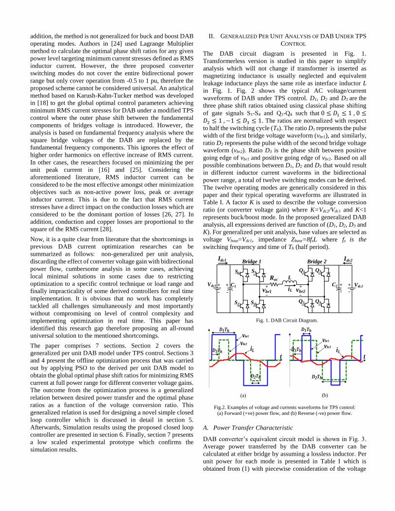
The DAB circuit diagram is presented in Fig. 1.
Transformerless version is studied in this paper to simplify
analysis which will not change if transformer is inserted as
magnetizing inductance is usually neglected and equivalent
leakage inductance plays the same role as interface inductor L
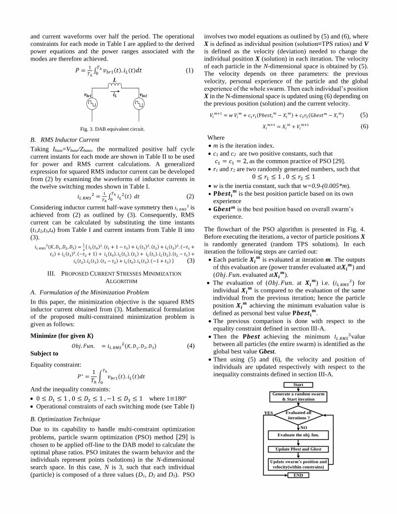
in Fig. 1. Fig. 2 shows the typical AC voltage/current
waveforms of DAB under TPS control. D1, D2 and D3 are the
three phase shift ratios obtained using classical phase shifting
of gate signals S1-S4 and Q1-Q4 such that 0 ≤ 𝐷1 ≤ 1 , 0 ≤𝐷2 ≤ 1 , −1 ≤ 𝐷3 ≤ 1. The ratios are normalized with respect
to half the switching cycle (Th). The ratio D1 represents the pulse
width of the first bridge voltage waveform (vbr1), and similarly,
ratio D2 represents the pulse width of the second bridge voltage
waveform (vbr2). Ratio D3 is the phase shift between positive
going edge of vbr1 and positive going edge of vbr2. Based on all
possible combinations between D1, D2 and D3 that would result
in different inductor current waveforms in the bidirectional
power range, a total of twelve switching modes can be derived.
The twelve operating modes are generically considered in this
paper and their typical operating waveforms are illustrated in
Table I. A factor K is used to describe the voltage conversion
ratio (or converter voltage gain) where K=Vdc2/Vdc1 and K<1
represents buck/boost mode. In the proposed generalized DAB
analysis, all expressions derived are function of (D1, D2, D3 and
K). For generalized per unit analysis, base values are selected as
voltage Vbase=Vdc1, impedance Zbase=8fsL where fs is the
switching frequency and time of Th (half period).
Fig. 1. DAB Circuit Diagram.
(a)
(b)
Fig.2. Examples of voltage and currents waveforms for TPS control: (a) Forward (+ve) power flow, and (b) Reverse (-ve) power flow.
A. Power Transfer Characteristic
DAB converter’s equivalent circuit model is shown in Fig. 3.
Average power transferred by the DAB converter can be
calculated at either bridge by assuming a lossless inductor. Per
unit power for each mode is presented in Table I which is
obtained from (1) with piecewise consideration of the voltage
vbr1
S1
S2
S3
S4
+
Q1
Q2
Q3
Q4
vbr2
Vdc2Vdc1 C1 C2
Bridge 1 Bridge 2
L
+++++iL
Idc2Idc1
Rac
iL
t
vbr1
vbr2
D1Th
D2Th
D3Th iLvbr2
vbr1
t
D1Th
D2Th
-D3Th
and current waveforms over half the period. The operational
constraints for each mode in Table I are applied to the derived
power equations and the power ranges associated with the
modes are therefore achieved.
𝑃 =1
𝑇ℎ∫ 𝑣𝑏𝑟1(𝑡). 𝑖𝐿(𝑡)𝑑𝑡𝑇ℎ0
(1)
Fig. 3. DAB equivalent circuit.
B. RMS Inductor Current
Taking Ibase=Vbase/Zbase, the normalized positive half cycle
current instants for each mode are shown in Table II to be used
for power and RMS current calculations. A generalized
expression for squared RMS inductor current can be developed
from (2) by examining the waveforms of inductor currents in
the twelve switching modes shown in Table I.
𝑖𝐿 𝑅𝑀𝑆2 =
1
𝑇ℎ∫ 𝑖𝐿
2(𝑡)𝑇ℎ0
𝑑𝑡 (2)
Considering inductor current half-wave symmetry then 𝑖𝐿 𝑅𝑀𝑆2 is
achieved from (2) as outlined by (3). Consequently, RMS
current can be calculated by substituting the time instants
(t1,t2,t3,t4) from Table I and current instants from Table II into
(3).
𝑖𝐿 𝑅𝑀𝑆2(𝐾,𝐷1, 𝐷2, 𝐷3) =
1
3{ 𝑖𝐿(𝑡0)
2. (𝑡1 + 1 − 𝑡3) + 𝑖𝐿(𝑡1)2. (𝑡2) + 𝑖𝐿(𝑡2)
2. (−𝑡1 +
𝑡3) + 𝑖𝐿(𝑡3)2. (−𝑡2 + 1) + 𝑖𝐿(𝑡0). 𝑖𝐿(𝑡1). (𝑡1) + 𝑖𝐿(𝑡1). 𝑖𝐿(𝑡2). (𝑡2 − 𝑡1) +
𝑖𝐿(𝑡2). 𝑖𝐿(𝑡3). (𝑡3 − 𝑡2) + 𝑖𝐿(𝑡0). 𝑖𝐿(𝑡3). (−1 + 𝑡3) } (3)
III. PROPOSED CURRENT STRESSES MINIMIZATION
ALGORITHM
A. Formulation of the Minimization Problem
In this paper, the minimization objective is the squared RMS
inductor current obtained from (3). Mathematical formulation
of the proposed multi-constrained minimization problem is
given as follows:
Minimize (for given K)
𝑂𝑏𝑗. 𝐹𝑢𝑛. = 𝑖𝐿 𝑅𝑀𝑆2(𝐾, 𝐷1, 𝐷2, 𝐷3) (4)
Subject to
Equality constraint:
𝑃∗ =1
𝑇ℎ∫ 𝑣𝑏𝑟1(𝑡). 𝑖𝐿(𝑡)𝑑𝑡𝑇ℎ
0
And the inequality constraints:
0 ≤ 𝐷1 ≤ 1 , 0 ≤ 𝐷2 ≤ 1 , −1 ≤ 𝐷3 ≤ 1 where 1≡180º
Operational constraints of each switching mode (see Table I)
B. Optimization Technique
Due to its capability to handle multi-constraint optimization
problems, particle swarm optimization (PSO) method [29] is
chosen to be applied off-line to the DAB model to calculate the
optimal phase ratios. PSO imitates the swarm behavior and the
individuals represent points (solutions) in the N-dimensional
search space. In this case, N is 3, such that each individual
(particle) is composed of a three values (D1, D2 and D3). PSO
involves two model equations as outlined by (5) and (6), where
X is defined as individual position (solution≡TPS ratios) and V
is defined as the velocity (deviation) needed to change the
individual position X (solution) in each iteration. The velocity
of each particle in the N-dimensional space is obtained by (5).
The velocity depends on three parameters: the previous
velocity, personal experience of the particle and the global
experience of the whole swarm. Then each individual’s position
X in the N-dimensional space is updated using (6) depending on
the previous position (solution) and the current velocity.
𝑉𝑖𝑚+1 = 𝑤 𝑉𝑖
𝑚 + 𝑐1𝑟1(P𝑏𝑒𝑠𝑡𝑖𝑚 − 𝑋𝑖
𝑚) + 𝑐2𝑟2(G𝑏𝑒𝑠𝑡𝑚 − 𝑋𝑖
𝑚) (5)
𝑋𝑖𝑚+1 = 𝑋𝑖
𝑚 + 𝑉𝑖𝑚+1 (6)
Where
m is the iteration index.
c1 and c2 are two positive constants, such that
𝑐1 = 𝑐1 = 2, as the common practice of PSO [29].
r1 and r2 are two randomly generated numbers, such that
0 ≤ 𝑟1 ≤ 1 , 0 ≤ 𝑟2 ≤ 1
w is the inertia constant, such that w=0.9-(0.005*m).
𝐏𝒃𝒆𝒔𝒕𝐢𝐦
is the best position particle based on its own
experience
𝐆𝒃𝒆𝒔𝒕𝒎 is the best position based on overall swarm’s
experience.
The flowchart of the PSO algorithm is presented in Fig. 4.
Before executing the iterations, a vector of particle positions X
is randomly generated (random TPS solutions). In each
iteration the following steps are carried out:
Each particle 𝑿𝒊𝒎 is evaluated at iteration m. The outputs
of this evaluation are (power transfer evaluated at𝑿𝒊𝒎) and
(𝑂𝑏𝑗. 𝐹𝑢𝑛. evaluated at𝑿𝒊𝒎).
The evaluation of (𝑂𝑏𝑗. 𝐹𝑢𝑛. at 𝑿𝒊𝒎) i.e. (𝑖𝐿 𝑅𝑀𝑆
2) for
individual 𝑿𝒊𝒎 is compared to the evaluation of the same
individual from the previous iteration; hence the particle
position 𝑿𝒊𝒎 achieving the minimum evaluation value is
defined as personal best value 𝐏𝒃𝒆𝒔𝒕𝐢𝐦
.
The previous comparison is done with respect to the
equality constraint defined in section III-A.
Then the 𝐏𝒃𝒆𝒔𝒕 achieving the minimum 𝐼𝐿 𝑅𝑀𝑆2value
between all particles (the entire swarm) is identified as the
global best value Gbest.
Then using (5) and (6), the velocity and position of
individuals are updated respectively with respect to the
inequality constraints defined in section III-A.
br1 br2L
Start
NO
Evaluate the obj. fun.
END
Generate a random swarm
& Start iteration
Evaluated all
iterations ?
Update Pbest and Gbest
Update swarm’s position and
velocity(within constrains)
YES

Fig. 4. Flow chart of PSO.
The previous steps are carried out for all the possible switching
modes according to the reference power P*. After all iteration
are executed, the Gbest is identified which includes the
optimal TPS ratios hence minimum 𝐼𝐿 𝑅𝑀𝑆2 is obtained with
accompanied switching mode.
TABLE I DAB MODES OF OPERATION & PER UNIT POWER EQUATIONS USING TPS CONTROL
Mode 1 Mode 1' Mode 2 Mode 2'
Waveforms
Normalized
time instants
to Th
𝑡0 = 0, 𝑡1 = 𝐷3, 𝑡2 = 𝐷2 + 𝐷3 𝑡3 = 𝐷1, 𝑡4 = 1
𝑡0 = 0, 𝑡1 = 𝐷3 + 1, 𝑡2 = 𝐷2 + 𝐷3 + 1 𝑡3 = 𝐷1, 𝑡4 = 1
𝑡0 = 0, 𝑡1 = 𝐷1, 𝑡2 = 𝐷2 + 𝐷3 − 1 𝑡3 = 𝐷3, 𝑡4 = 1
𝑡0 = 0, 𝑡1 = 𝐷1, 𝑡2 = 𝐷2 + 𝐷3 𝑡3 = 𝐷3 + 1, 𝑡4 = 1
Operational
Constraints
𝐷1 ≥ 𝐷2
0 ≤ 𝐷3 ≤ 𝐷1 − 𝐷2
𝐷1 ≥ 𝐷2
0 ≤ 𝐷3 + 1 ≤ 𝐷1 − 𝐷2
𝐷2 ≥ 𝐷1
(1 + 𝐷1 − 𝐷2) ≤ 𝐷3 ≤ 1
𝐷2 ≥ 𝐷1
(1 + 𝐷1 − 𝐷2) ≤ 𝐷3 + 1 ≤ 1
Power
Transfer
𝑃 = 2𝐾(𝐷2 2 − 𝐷1𝐷2 + 2𝐷2𝐷3) 𝑃 = −2𝐾(𝐷2
2 − 𝐷1𝐷2 + 2𝐷2(𝐷3 + 1)) 𝑃 = 2𝐾(𝐷1 2 − 𝐷1𝐷2 + 2𝐷1 − 2𝐷1𝐷3) 𝑃 = −2𝐾(𝐷1
2 − 𝐷1𝐷2 − 2𝐷1𝐷3)
Power
Range
𝑃𝑚𝑎𝑥 = 0.5𝐾 pu , 𝑃𝑚𝑖𝑛 = −0.5𝐾 pu 𝑃𝑚𝑎𝑥 = 0.5𝐾 pu , 𝑃𝑚𝑖𝑛 = −0.5𝐾 pu 𝑃𝑚𝑎𝑥 = 0.5𝐾 pu , 𝑃𝑚𝑖𝑛 = −0.5𝐾 pu 𝑃𝑚𝑎𝑥 = 0.5𝐾 pu , 𝑃𝑚𝑖𝑛 = −0.5𝐾 pu
Mode 3 Mode 3' Mode 4 Mode 4'
Waveforms
Normalized
time instants
to Th
𝑡0 = 0, 𝑡1 = 𝐷1, 𝑡2 = 𝐷3 𝑡3 = 𝐷2+𝐷3, 𝑡4 = 1
𝑡0 = 0, 𝑡1 = 𝐷1, 𝑡2 = 𝐷3 + 1 𝑡3 = 𝐷2+𝐷3 + 1, 𝑡4 = 1
𝑡0 = 0, 𝑡1 = 𝐷2 + 𝐷3 − 1, 𝑡2 = 𝐷1 𝑡3 = 𝐷3, 𝑡4 = 1
𝑡0 = 0, 𝑡1 = 𝐷2 + 𝐷3, 𝑡2 = 𝐷1 𝑡3 = 𝐷3 + 1, 𝑡4 = 1
Operational
Constraints
𝐷2 ≤ 1 − 𝐷1
𝐷1 ≤ 𝐷3 ≤ 1 − 𝐷2
𝐷2 ≤ 1 − 𝐷1
𝐷1 ≤ 𝐷3 + 1 ≤ 1 − 𝐷2
𝐷1 ≤ 𝐷3 ≤ 1
1 − 𝐷3 ≤ 𝐷2 ≤ 1 − 𝐷3 + 𝐷1
𝐷1 ≤ 𝐷3 + 1 ≤ 1
−𝐷3 ≤ 𝐷2 ≤ −𝐷3 + 𝐷1
Power
Transfer
𝑃 = 2𝐾(𝐷1𝐷2) 𝑃 = −2𝐾(𝐷1𝐷2) 𝑃 = 2𝐾(−𝐷2 2−𝐷3
2 + 2𝐷2 + 2𝐷3
−2𝐷2𝐷3 + 𝐷1𝐷2 − 1) 𝑃 = −2𝐾(−𝐷2
2 − (𝐷3 + 1)2
+2𝐷3 − 2𝐷2𝐷3 + 𝐷1𝐷2 + 1)
Power
Range
𝑃𝑚𝑎𝑥 = 0.5𝐾 pu, 𝑃𝑚𝑖𝑛 = 0.0 pu 𝑃𝑚𝑎𝑥 = 0.0 pu, 𝑃𝑚𝑖𝑛 = −0.5𝐾 pu 𝑃𝑚𝑎𝑥 = 0.667𝐾 pu, 𝑃𝑚𝑖𝑛 = 0.0 pu 𝑃𝑚𝑎𝑥 = 0.0 pu, 𝑃𝑚𝑖𝑛 = −0.667𝐾 pu
Mode 5 Mode 5' Mode 6 Mode 6'
Waveforms
Normalized
time instants
to Th
𝑡0 = 0, 𝑡1 = 𝐷3, 𝑡2 = 𝐷1 𝑡3 = 𝐷2 + 𝐷3, 𝑡4 = 1
𝑡0 = 0, 𝑡1 = 𝐷3 + 1, 𝑡2 = 𝐷1 𝑡3 = 𝐷2 + 𝐷3 + 1, 𝑡4 = 1
𝑡0 = 0, 𝑡1 = 𝐷2 + 𝐷3 − 1, 𝑡2 = 𝐷3 𝑡3 = 𝐷1, 𝑡4 = 1
𝑡0 = 0, 𝑡1 = 𝐷2 + 𝐷3, 𝑡2 = 𝐷3 + 1 𝑡3 = 𝐷1 , 𝑡4 = 1
Operational
Constraints
𝐷1 − 𝐷3 ≤ 𝐷2 ≤ 1 − 𝐷3
0 ≤ 𝐷3 ≤ 𝐷1
𝐷1 − 𝐷3 − 1 ≤ 𝐷2 ≤ −𝐷3
0 ≤ 𝐷3 + 1 ≤ 𝐷1
1 − 𝐷2 ≤ 𝐷1
1 − 𝐷2 ≤ 𝐷3 ≤ 𝐷1
1 − 𝐷2 ≤ 𝐷1
1 − 𝐷2 ≤ 𝐷3 + 1 ≤ 𝐷1
Power
Transfer
𝑃 = 2𝐾(−𝐷1 2 − 𝐷3
2 + 𝐷1𝐷2
+2𝐷1𝐷3) 𝑃 = −2𝐾(−𝐷1
2 − (𝐷3 + 1)2
+𝐷1𝐷2 + 2𝐷1(𝐷3 + 1)) 𝑃 = 2𝐾(−𝐷1
2 − 𝐷2 2−2𝐷3
2 + 2𝐷3
−2𝐷2𝐷3 + 𝐷1𝐷2 + 2𝐷1𝐷3 + 2𝐷2 − 1) 𝑃 = −2𝐾(−𝐷1
2 − 𝐷2 2 − 2(𝐷3 + 1)
2
+2𝐷3 − 2𝐷2𝐷3 + 𝐷1𝐷2
+2𝐷1(𝐷3 + 1) + 1)
Power
Range
𝑃𝑚𝑎𝑥 = 0.667𝐾 pu , 𝑃𝑚𝑖𝑛 = 0.0 pu 𝑃𝑚𝑎𝑥 = 0.0 pu, 𝑃𝑚𝑖𝑛 = −0.667𝐾 pu 𝑃𝑚𝑎𝑥 = 𝐾 pu, 𝑃𝑚𝑖𝑛 = 0.0 pu 𝑃𝑚𝑎𝑥 = 0.0 pu, 𝑃𝑚𝑖𝑛 = −𝐾 pu
iL
t0 t1
t
t2 t3 t4 t5 t6 t7 t8
vbr1
vbr2
D1Th
D2Th
D3Th
t0 t1 t2t3 t4 t5 t6 t7 t8
t
D1Th
-D3Th
D2Thvbr1 vbr2
iL iL
t
t0 t1 t2 t3 t4 t5 t6 t7 t8
vbr1 vbr2
D1ThD2Th
D3ThiL
t0 t1 t2 t3 t4 t5 t6 t7 t8
vbr2
vbr1
t
D1Th
D2Th
-D3Th
t
iL
t0 t1 t2 t3 t4 t5 t6 t7 t8
vbr2
vbr1
D1ThD2Th
D3Th iL
t
vbr1 vbr2
t8t6t5t4t3t2t1t0 t7
D2Th
D1Th
-D3ThiL
t0 t1 t2 t3 t4 t5 t7t6
t
t8
vbr2 vbr1
D1ThD2Th
D3Th
t
vbr1 vbr2
iL
t8t7t6t5t4t3t2t1t0
D1Th
-D3Th
D2Th
iL
t
vbr2 vbr2
t0 t1 t2 t3 t4 t5 t6 t7 t8
D1ThD2Th
D3ThiL
t
vbr1 vbr2
t0 t1 t2 t3 t5 t6 t7t4 t8
D1Th
-D3Th
D2Th
t0 t1
iL
t2 t3 t4 t5 t6 t7 t8
vbr2 vbr1
t
D3Th
D1ThD2Th
iL
t0
t
vbr1 vbr2
t1 t2 t3 t4 t5 t6 t7 t8
D1ThD2Th
-D3Th

TABLE II
PER UNIT INDUCTOR CURRENTS (IL) FOR POSITIVE HALF CYCLE SWITCHING INTERVALS NORMALIZED TO IBASE Modes iL(t0) iL(t1) iL(t2) iL(t3)
1 −(𝐷1 − 𝐾𝐷2) (−𝐷1 + 2𝐷3 + 𝐾𝐷2) (−𝐷1 + 2𝐷2 + 2𝐷3 − 𝐾𝐷2) (𝐷1 − 𝐾𝐷2)
1’ −(𝐷1 + 𝐾𝐷2) (−𝐷1 + 2(𝐷3 + 1) − 𝐾𝐷2) (−𝐷1 + 2𝐷2 + 2(𝐷3 + 1) + 𝐾𝐷2) (𝐷1 + 𝐾𝐷2)
2 −(𝐷1 − 2𝐾 + 𝐾𝐷2 + 2𝐾𝐷3) (𝐷1 + 2𝐾𝐷1 − 𝐾𝐷2 + 2𝐾 − 2𝐾𝐷3) (𝐷1 + 𝐾𝐷2) (𝐷1 + 𝐾𝐷2)
2’ −(𝐷1 + 2𝐾 −𝐾𝐷2 − 2𝐾(𝐷3 + 1)) (𝐷1 − 2𝐾 − 2𝐾𝐷1 + 𝐾𝐷2 + 2𝐾(𝐷3 + 1)) (𝐷1 − 𝐾𝐷2) (𝐷1 − 𝐾𝐷2)
3 −(𝐷1 − 𝐾𝐷2) (𝐷1 + 𝐾𝐷2) (𝐷1 + 𝐾𝐷2) (𝐷1 − 𝐾𝐷2)
3’ −(𝐷1 + 𝐾𝐷2) (𝐷1 − 𝐾𝐷2) (𝐷1 − 𝐾𝐷2) (𝐷1 + 𝐾𝐷2)
4 −(𝐷1 − 2𝐾 + 𝐾𝐷2 + 2𝐾𝐷3) (−𝐷1 − 2 + 2𝐷2 +𝐾𝐷2 + 2𝐷3) (𝐷1 + 𝐾𝐷2) (𝐷1 + 𝐾𝐷2)
4’ −(𝐷1 + 2𝐾 −𝐾𝐷2 − 2𝐾(𝐷3 + 1)) (−𝐷1 − 2+ 2𝐷2 + 2(𝐷3 + 1) − 𝐾𝐷2) (𝐷1 − 𝐾𝐷2) (𝐷1 − 𝐾𝐷2)
5 −(𝐷1 − 𝐾𝐷2) (−𝐷1 + 2𝐷3 + 𝐾𝐷2) (𝐷1 − 2𝐾𝐷1 +𝐾𝐷2 + 2𝐾𝐷3) (𝐷1 − 𝐾𝐷2)
5’ −(𝐷1 + 𝐾𝐷2) (−𝐷1 + 2(𝐷3 + 1) − 𝐾𝐷2) (𝐷1 + 2𝐾𝐷1 − 𝐾𝐷2 − 2𝐾(𝐷3 + 1)) (𝐷1 + 𝐾𝐷2)
6 −(𝐷1 + 𝐾𝐷2 + 2𝐾𝐷3 − 2𝐾) (−𝐷1 + 2𝐷2 + 2𝐷3 + 𝐾𝐷2 − 2) (−𝐷1 + 2𝐷3 +𝐾𝐷2) (𝐷1 − 2𝐾𝐷1 +𝐾𝐷2 + 2𝐾𝐷3)
6’ −(𝐷1 − 𝐾𝐷2 − 2𝐾(𝐷3 + 1) + 2𝐾) (−𝐷1 + 2𝐷2 + 2(𝐷3 + 1) − 𝐾𝐷2 − 2) (−𝐷1 + 2(𝐷3 + 1) − 𝐾𝐷2) (𝐷1 + 2𝐾𝐷1 − 𝐾𝐷2 − 2𝐾(𝐷3 + 1))
IV. PSO OFF-LINE ALGORITHM ANALYSIS
The off-line optimal phase shift calculations were carried out
using MATLAB software, based on the proposed per unit DAB
equations and constraints. Assuming that K=Vdc2/Vdc1 and K≤1,
the other condition K>1 can be analyzed similarly. The
buck/boost mode is included in this paper as bi-directional
power at K<1 inherently includes buck mode for operation in
forward power flow and boost mode for operation in reverse
power flow. The values of voltage conversion ratio (K) used in
this section were:
K=0.25, 0.4 and 0.6 representing buck/boost mode.
K=1 representing unity gain operating mode.
The optimal solutions of the three phase ratios are presented in
Fig. 5 parts (a) to (c) and Fig. 6 where the full per unit power
range is from –K to K; such that |Pmax-pu| =K. This is calculated
by normalizing the DAB maximum power transfer from (7) to
the base power expressed in (8). The PSO is applied in the entire
power range for both power flow directions; such that positive
power transfer indicates power flow from bridge 1 to bridge 2
and vice versa. A general pattern for the optimal phase shifts
ratios in buck/boost mode is developed in Fig. 5 (d) where the
entire power range is divided into four sections.
𝑃𝑚𝑎𝑥 =𝑉𝑑𝑐1 𝑉𝑑𝑐2
8 𝑓𝑠𝐿 , Where 𝑉𝑑𝑐2 = 𝐾𝑉𝑑𝑐1 (7)
𝑃𝑏𝑎𝑠𝑒 =𝑉𝑏𝑎𝑠𝑒
2
𝑍𝑏𝑎𝑠𝑒 =𝑉𝑑𝑐1
2
8 𝑓𝑠𝐿 (8)
Regarding the optimal solutions in buck/boost mode shown in
Fig. 5 parts (a) to (c):
If desired power|𝑷∗| ≤ 𝟎. 𝟓𝑲, optimal solutions were
attained by (TPS) where minimum 𝑖𝐿 𝑅𝑀𝑆 is achieved by the
switching modes 2’ as shown in Fig. 5 (d).
If desired power |𝑷∗| ≥ 𝟎. 𝟓𝑲, extended phase shift (EPS)
[16] and conventional phase shift (CPS) achieved the optimal
solution, as shown in Fig. 5 (d), where the minimum 𝑖𝐿 𝑅𝑀𝑆 is
realized by switching modes 6 and 6’ for positive and negative
power transfer respectively.
On the other hand, Fig. 6 shows that the conventional phase
shift (CPS) [1] fulfills optimal solutions for unity gain operating
mode at the entire loading range at both power flow directions.
In this special case, the optimal solutions were attained by mode
6 or mode 6’ with D1=D2=1.
(a)
(b)
(c)
(d)
Fig. 5. Application of PSO to the DAB for buck/boost mode: (a)-(c) Optimal phase shift ratios at K=0.25, 0.4 and 0.6 respectively
(d) General pattern of optimal TPS at buck/boost mode.
D1,
D2
&D
3
K=0.25
Power P* [pu]-0.25 -0.15 -0.05 0.0 0.05 0.15 0.25
-0.8
-0.6
-0.4
-0.2
0.0
0.2
0.4
0.6
0.8
1
D1
D2
D3
-0.4 -0.25 -0.1 0.0 0.1 0.25 0.4-0.6
-0.4
-0.2
0
0.2
0.4
0.6
0.8
1
D1 &
D2 &
D3
K=0.4
D1
D2
D3
K=0.4
Power P* [pu]
D1,
D2
&D
3
-0.6 -0.4 -0.2 0.0 0.2 0.4 0.6
-0.4
-0.2
0
0.2
0.4
0.6
0.8
1
K=0.6
D1
D2
D3
K=0.6
D1, D
2&
D3
Power P* [pu]
-K<P*<-0.5K -0.5K<P*<0
Power P* [pu]
CPS, EPS
Mode 6'
TPS
Mode 2'
EPS, CPS
Mode 6
+K-K
TPS
Mode 2'
0.5K<P*<K0<P*<0.5K
D1∝P*
D2= 1 D2= D1 / K D2= D1 / K D2= 1
D1∝P* D1∝ P* D1∝ P*

Fig. 6. Optimal phase shift ratios unity gain mode K=1.
V. CLOSED LOOP CONTROL DESIGN
The extensive set of optimal TPS ratios, presented in previous
section, presents a generic data pool. This data is carefully
analyzed to derive simple relations which are used to design the
generalized closed loop control scheme presented in Fig. 7.
In buck/boost mode, D1 can be regulated through a PI controller
as the relation between power and D1 is almost linear
throughout which can be noticed in Fig. 5 parts (a) to (c).
Whereas the relationship between the other control parameters
(D2 and D3) and power is non-linear and dependent on the
power level.
The following relations can be concluded from Fig. 5 parts (a)
to (c):
For|𝑷∗| ≥ 𝟎. 𝟓𝑲: optimal value of D2 is (D2=1). The
value of D3 is highly non-linear and therefore can only be
calculated from re-arranging mode 6 and mode 6’ power
equations in Table I. For forward power flow this is shown
in (9.a), and for reverse power flow this is shown in (9.b).
For|𝑷∗| < 𝟎. 𝟓𝑲: optimal value of D2 is D2=D1/K. The
value of D3 is highly non-linear and therefore can only be
calculated from re-arranging mode 2’ power equation in
Table I. The calculation of D3 in this section is shown in
(9.c) for both forward and reverse power flow.
𝐷3 =
{
−(−1 + 𝐷2 − 𝐷1) − √2𝐷1 + 2𝐷2 − 𝐷1
2 − 𝐷22 −
𝑃∗
𝐾 − 1
2 , 𝑓𝑜𝑟 𝑃∗ ≥ 0.5𝐾
−(1 + 𝐷2 − 𝐷1) + √2𝐷1 + 2𝐷2 − 𝐷12 − 𝐷2
2 +𝑃∗
𝐾 − 1
2 , 𝑓𝑜𝑟 𝑃∗ ≤ −0.5𝐾
0.5 (𝐷1 − 𝐷2 +𝑃∗
2𝐾𝐷1) , 𝑓𝑜𝑟 − 0.5𝐾 < 𝑃∗ < 0.5𝐾
(9.a)
(9.b)
(9.c)
In unity gain mode, Fig. 6 shows that both DAB bridge AC
voltages are full square waves (D1=D2=1) for the entire
bidirectional power range and the only control needed to
regulate power flow is on D3. This can be implemented using a
PI controller because the relation between the power level and
value of the third phase shift D3 is almost linear as depicted in
Fig. 6.
The close-loop variable is the sending end power (Pse) such that
Pse=Pbr1 for positive power flow while Pse=Pbr2 for negative
power flow, where Pbr1 and Pbr2 are the H-bridge powers
measured at the DC sides of bridges 1 and 2 respectively.
Fig. 7. Proposed control scheme for the DAB.
VI. SIMULATION RESULTS
To confirm the presented analysis, detailed simulations using
SIMULINK/MATLAB platform software were performed. The
simulations were carried out for the buck/boost/unity operating
modes using the DAB parameters described in Table III.
TABLE III
PARAMETERS OF THE EXPERIMENTAL SETUP
Parameter value
Bridge 1 DC Voltage Vdc1 100V
Bridge 2 DC Voltage Vdc2 K*100V
Switching Frequency fs 2.5kHz
Base Power Pbase 500W
Interface inductor L 1mH
A. Effectiveness of the proposed control scheme
The effectiveness of the proposed control algorithm to track
reference power level while maintaining minimum current
stresses is verified in this section by applying bidirectional step
changes of reference power level at various voltage conversion
ratios. The results are presented in Fig. 8, where the sending end
power is measured and plotted against the reference power level.
In addition, associated measured RMS inductor current (𝑖𝐿 𝑎𝑐𝑡) is shown along with the minimum possible RMS inductor
current (𝑖𝐿 𝑚𝑖𝑛) calculated offline by the PSO. It can be noticed
that the proposed power flow controller is capable of tracking
the bidirectional reference power level at different voltage
conversion ratios. Moreover (𝑖𝐿 𝑎𝑐𝑡) is maintained very close to
(𝑖𝐿 𝑚𝑖𝑛) which confirms minimum losses.
-1 -0.8 -0.6 -0.4 -0.2 0 0.2 0.4 0.6 0.8 1-0.5
-0.35
-0.2
-0.05
0.1
0.25
0.4
0.55
0.7
0.85
1
K=1
D1
D2
D3
Power P* [pu]
D1,
D2
&D
3
K=1
D2=1
D3 is calculated
from (9.a)
NO YES
YES YESNONO
D2=(D1/ K)
D3 is calculated
from (9.c)
D2=(D1/ K)
D3 is calculated
from (9.c)
D2=1
D3 is calculated
from (9.b)
Get K, P*, PI Output
P*≤ -K/2 P*> 0
Operating
Mode?
D1=D2=1
D3=PI Output
K=1
D1=PI Output
P*≥ K/2
K<1
Unity Gain Mode
Buck/Boost Mode
PI D1
D2
D3
S1S2S3S4Q1Q2Q3Q4
DAB
Switching
Signals
PseK
Phase Shift
Calculation
TP
S M
od
ula
tor
-+P*
Send D1, D2 & D3 to
TPS Modulator

B. Comparative analysis with other phase shift methods
A comprehensive comparison between the proposed phase shift
technique and other phase shift techniques in literature is
provided in this section. The phase shift techniques to compare
the proposed phase shift technique with are: Conventional phase
shift (CPS) [1], Dual phase shift (DPS) [15], Extended phase
shift (EPS) [16], Extended dual phase shift (EDPS) [22], Triple
phase shift [28] and Unified phase shift [24]. The entire per unit
bi-directional power range (-K pu to K pu) is considered in all
techniques. The RMS inductor current is compared for all
mentioned techniques at different voltage conversion ratios K as
shown in Fig.9. The current is the main factor affecting the
efficiency; hence it is displayed first where the proposed phase
shift technique is achieving the lowest current stresses.
Moreover, efficiency calculations, outlined by (10), have been
carried out in simulations at the DC side to include switching
and copper losses. The DAB circuit diagram shown in Fig.1 is
used in the simulation where the variables used for efficiency
calculation (Vdc1, Idc1, Vdc2, Idc2) are shown along with the
parasitic resistance (AC link) resistance (Rac). The values for
this resistance is chosen carefully to produce reliable results
such that Rac=0.06pu, where Zbase =8fswL. The efficiency curves,
presented in Fig.10, show that the proposed method achieves
better performance than other existing phase shift schemes.
𝑒𝑓𝑓𝑖𝑐𝑖𝑒𝑛𝑐𝑦 =𝑃𝑟𝑒𝑃𝑠𝑒
=
{
𝑖𝑓 𝑃∗ > 0 𝑡ℎ𝑒𝑛 {
𝑃𝑠𝑒 = 𝑉𝑑𝑐1𝐼𝑑𝑐1,𝑎𝑣𝑔 𝑃𝑟𝑒 = 𝑉𝑑𝑐2𝐼𝑑𝑐2,𝑎𝑣𝑔
𝑖𝑓 𝑃∗ < 0 𝑡ℎ𝑒𝑛 { 𝑃𝑠𝑒 = 𝑉𝑑𝑐2𝐼𝑑𝑐2,𝑎𝑣𝑔 𝑃𝑟𝑒 = 𝑉𝑑𝑐1𝐼𝑑𝑐1,𝑎𝑣𝑔
(10)
(a)
(b)
Fig.10. Efficiency curves using existing phase shift techniques and the proposed TPS controller: (a) K=0.2, (b) K=0.4
Eff
icie
ncy
(%
)
Transferred Power [pu]
0.07 0.09 0.11 0.13 0.15 0.17 0.1960
65
70
75
80
85
90
CPS[1]
DPS[15]
EPS[16]
EDPS[22]
TPS[28]
UPS[24]
Proposed TPS Controller
Transferred Power [pu]
Eff
icie
ncy
(%
)
0.1 0.15 0.2 0.25 0.3 0.3582
84
86
88
90
92
94
CPS[1]
DPS[15]
EPS[16]
EDPS[22]
TPS[28]
UPS[24]
Proposed TPS Controller
(a)
(b)
(c) Fig. 8: Response of power transfer with current stresses at different power levels for different voltage conversion ratios: (a) K=0.4 (b) K=0.6 (c) K=1.
(a)
(b)
(c)
Fig. 9: Curves of current stress iL RMS with respect to P* and K in CPS[1], DPS[15], EPS[16], EDPS[22], TPS[28], UPS[24] and proposed TPS controller at:
(a) K=0.2, (b) K=0.3, (c) K=0.4.
0 0.15 0.3
-0.3
-0.1
0.1
0.3
0.5
P*
Pse
K=0.4
iL min=1.21 pu
iL act=1.23 pu
iL min=0.66 pu
iL act=0.68 pu
iL min=0.38 pu
iL act=0.41 pu
Time (s)
Pow
er (
pu
)
0 0.15 0.3-0.4
-0.2
0
0.2
0.4
0.6
P*
Pse
K=0.6iL min=0.91 pu
iL act=0.919 pu
iL min=0.28 pu
iL act=0.285 pu
iL min=0.57 pu
iL act=0.581 pu
Pow
er (
pu
)
Time (s)0 0.15 0.3
-1
-0.7
-0.4
-0.1
0.2
0.5
0.8
P*
Pse
Time (s)
iL min=0.99 pu
iL act=1.01 pu
iL min=0.43 pu
iL act=0.44 pu
iL min=1.59 pu
iL act=1.604 pu
Po
wer
(pu
)
K=1
0.02 0.06 0.1 0.14 0.18 0.20.05
0.45
0.85
1.2
CPS[1]
DPS[15]
EPS[16]
EDPS[22]
TPS[28]
UPS[24]
Proposed TPS Controller
i L R
MS
[pu
]
Power (±P*)[pu]
0.03 0.09 0.15 0.21 0.27 0.30.05
0.45
0.85
1.2
CPS[1]
DPS[15]
EPS[16]
EDPS[22]
TPS[28]
UPS[24]
Proposed TPS Controller
i L R
MS
[pu
]
Power (±P*)[pu]0.04 0.12 0.2 0.28 0.36 0.4
0.05
0.45
0.85
1.21
CPS[1]
DPS[15]
EPS[16]
EDPS[22]
TPS[28]
UPS[24]
Proposed TPS Controller
Power (±P*)[pu]
i L R
MS
[pu
]
C. Robustness of the proposed control scheme
In order to test proposed controller robustness, simulations have
been implemented with values of inductor and its parasitic
resistance (L and Rac respectively) changing by ±10%. The
proposed controller is applied on the DAB circuit shown in
Fig.1, and simulated, for three cases:
L=1mH , Rac=1.2 Ω , 𝑃𝑟𝑎𝑡𝑒𝑑 =𝑉𝑑𝑐1 𝑉𝑑𝑐2
8 𝑓𝑠𝐿= 500 𝑊𝑎𝑡𝑡
L=1mH +10% , Rac =1.2 Ω+10% , 𝑃𝑟𝑎𝑡𝑒𝑑 =𝑉𝑑𝑐1 𝑉𝑑𝑐2
8 𝑓𝑠𝐿= 454.5 𝑊𝑎𝑡𝑡
L=1mH-10% , Rac =1.2 Ω-10% , 𝑃𝑟𝑎𝑡𝑒𝑑 =𝑉𝑑𝑐1 𝑉𝑑𝑐2
8 𝑓𝑠𝐿= 555.5 𝑊𝑎𝑡𝑡
The proposed controller response in terms of sending end power
Pse plotted against ref. power P* for the three cases listed above
are shown in Fig. 11. The simulation is carried out at three
different voltage conversion ratios K (K=0.4, 0.6 and 1) for each
of the three cases of parameter variation described. The DAB
response while parameters change show that the control
algorithm is stable and robust and can be applied to any DAB
converter regardless of rating and parameters. This is because
the proposed analysis is all per unit and generically
standardized.
VII. EXPERIMENTAL RESULTS
A low scaled experimental DAB setup was developed according
the schematic shown in Fig. 12 in order to validate the proposed
closed loop controller. The parameters used for designing the
test rig are listed in Table III. The entire analysis in the paper is
based on transformer-less DAB, as the main scope is the
derivation and implementation of new controller. The DAB is
based, in theory and experiment, on an AC inductor which is
fundamentally the equivalent model of a transformer’s leakage
inductance. Based on this, a 1mH air core inductance is
employed in the experimental rig while the semiconductor
switches used are MOSFETs (MOSFET IRF250).
A. Steady state response
Proposed control scheme is verified in this section at selected
steady state reference power levels for various voltage
conversion ratios K. Both bridge voltage (Vbr1, Vbr2) and
instantaneous inductor current (iL) are measured at the AC side
presented in Fig. 13 where the RMS inductor is measured and
displayed on the right hand side of the scope screenshot.
(a) (b) (c)
(d) (e) (f)
(g) (h) (i)
Fig. 11. Robustness of the proposed control algorithm to different system conditions
(a)K=0.4, L=1mH, Rac=1.2Ω, (b) K=0.4, L=1mH+10%,Rac=1.2Ω +10%, (c) K=0.4, L=1mH-10%, Rac =1.2Ω -10%, (d)K=0.6, L=1mH, Rac=1.2Ω, (e) K=0.6, L=1mH+10%,Rac=1.2Ω +10%, (f) K=0.6, L=1mH-10%, Rac =1.2Ω -10%,
(g)K=1.0, L=1mH, Rac=1.2Ω, (h) K=1.0, L=1mH+10%,Rac=1.2Ω +10%, (i) K=1.0,L=1mH-10%, Rac=1.2Ω -10%.
0 0.1 0.2 0.3 0.4-200
-150
-100
-50
0
50
100
150
200
250
Pse
P*P
ow
er
(Watt
)
Time (s)
0 0.1 0.2 0.3 0.4-150
-100
-50
0
50
100
150
200
Pse
P*
Time (s)
Pow
er (W
att
)
0 0.1 0.2 0.3 0.4-150
-100
-50
0
50
100
150
200
250
Pse
P*
Pow
er (W
att
)
Time (s)
0 0.1 0.2 0.3 0.4-200
-100
0
100
200
Pse
P*
Pow
er
(Wa
tt)
Time (s)
0 0.1 0.2 0.3 0.4-200
-100
0
100
200
Pse
P*
Time (s)
Pow
er (W
att
)
0 0.1 0.2 0.3 0.4-200
-100
0
100
200
300
Pse
P*
Po
wer
(W
att
)
Time (s)
0 0.1 0.2 0.3 0.4-400
-200
0
200
400
600
Pse
P*
Time (s)
Po
wer
(W
att
)
0 0.1 0.2 0.3 0.4-400
-300
-200
-100
0
100
200
300
400
500
Pse
P*
Pow
er
(Wa
tt)
Time (s)
0 0.1 0.2 0.3 0.4-600
-400
-200
0
200
400
600
Pse
P*
Time (s)P
ow
er (W
att
)
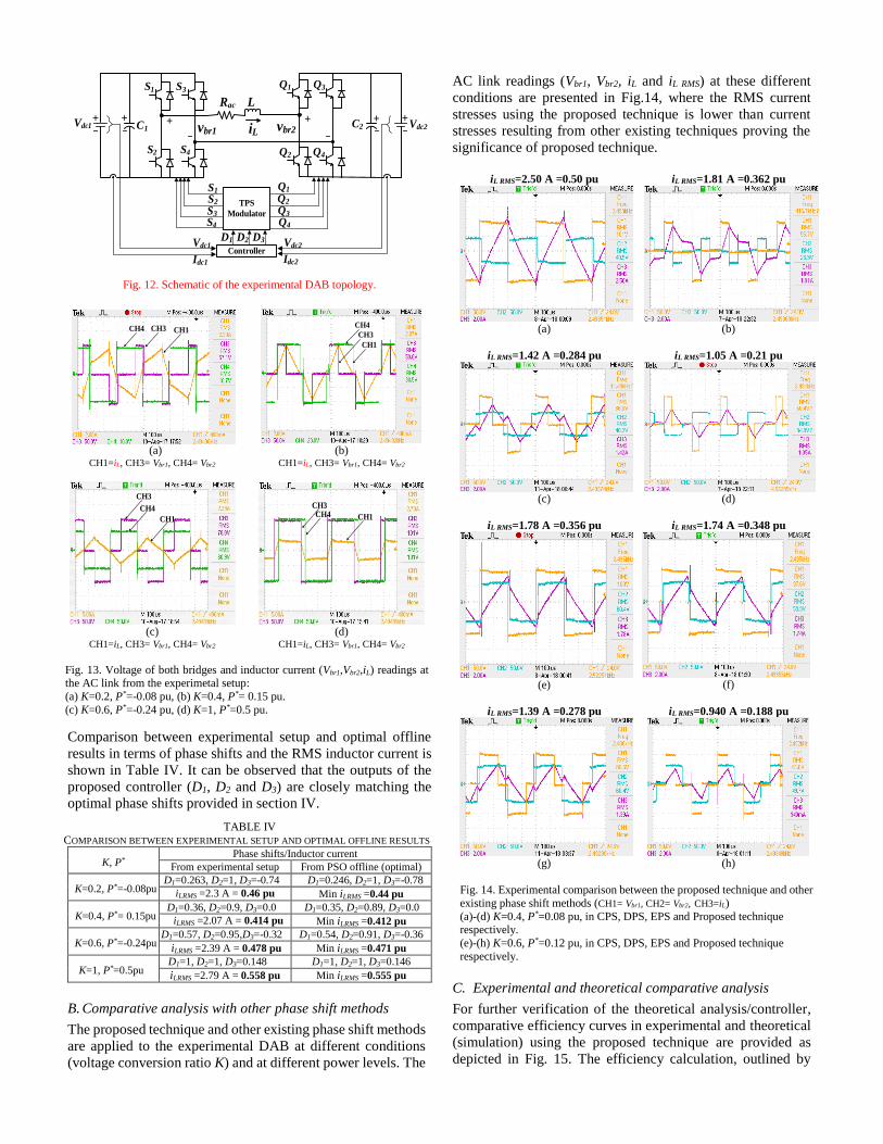
Fig. 12. Schematic of the experimental DAB topology.
(a)
CH1=iL, CH3= Vbr1, CH4= Vbr2
(b)
CH1=iL, CH3= Vbr1, CH4= Vbr2
(c)
CH1=iL, CH3= Vbr1, CH4= Vbr2
(d)
CH1=iL, CH3= Vbr1, CH4= Vbr2
Fig. 13. Voltage of both bridges and inductor current (Vbr1,Vbr2,iL) readings at the AC link from the experimetal setup:
(a) K=0.2, P*=-0.08 pu, (b) K=0.4, P*= 0.15 pu.
(c) K=0.6, P*=-0.24 pu, (d) K=1, P*=0.5 pu.
Comparison between experimental setup and optimal offline
results in terms of phase shifts and the RMS inductor current is
shown in Table IV. It can be observed that the outputs of the
proposed controller (D1, D2 and D3) are closely matching the
optimal phase shifts provided in section IV.
TABLE IV
COMPARISON BETWEEN EXPERIMENTAL SETUP AND OPTIMAL OFFLINE RESULTS
K, P* Phase shifts/Inductor current
From experimental setup From PSO offline (optimal)
K=0.2, P*=-0.08pu D1=0.263, D2=1, D3=-0.74 D1=0.246, D2=1, D3=-0.78
iLRMS =2.3 A = 0.46 pu Min iLRMS =0.44 pu
K=0.4, P*= 0.15pu D1=0.36, D2=0.9, D3=0.0 D1=0.35, D2=0.89, D3=0.0
iLRMS =2.07 A = 0.414 pu Min iLRMS =0.412 pu
K=0.6, P*=-0.24pu D1=0.57, D2=0.95,D3=-0.32 D1=0.54, D2=0.91, D3=-0.36
iLRMS =2.39 A = 0.478 pu Min iLRMS =0.471 pu
K=1, P*=0.5pu D1=1, D2=1, D3=0.148 D1=1, D2=1, D3=0.146
iLRMS =2.79 A = 0.558 pu Min iLRMS =0.555 pu
B. Comparative analysis with other phase shift methods
The proposed technique and other existing phase shift methods
are applied to the experimental DAB at different conditions
(voltage conversion ratio K) and at different power levels. The
AC link readings (Vbr1, Vbr2, iL and iL RMS) at these different
conditions are presented in Fig.14, where the RMS current
stresses using the proposed technique is lower than current
stresses resulting from other existing techniques proving the
significance of proposed technique.
iL RMS=2.50 A =0.50 pu iL RMS=1.81 A =0.362 pu
(a)
(b)
iL RMS=1.42 A =0.284 pu iL RMS=1.05 A =0.21 pu
(c)
(d)
iL RMS=1.78 A =0.356 pu iL RMS=1.74 A =0.348 pu
(e)
(f)
iL RMS=1.39 A =0.278 pu iL RMS=0.940 A =0.188 pu
(g)
(h)
Fig. 14. Experimental comparison between the proposed technique and other
existing phase shift methods (CH1= Vbr1, CH2= Vbr2, CH3=iL)
(a)-(d) K=0.4, P*=0.08 pu, in CPS, DPS, EPS and Proposed technique respectively.
(e)-(h) K=0.6, P*=0.12 pu, in CPS, DPS, EPS and Proposed technique
respectively.
C. Experimental and theoretical comparative analysis
For further verification of the theoretical analysis/controller,
comparative efficiency curves in experimental and theoretical
(simulation) using the proposed technique are provided as
depicted in Fig. 15. The efficiency calculation, outlined by
iLvbr1
S1
S2
S3
S4
LRac
Controller
+ ++
Q1
Q2
Q3
Q4
+vbr2
TPS
Modulator
D1 D2 D3
S1
S2
S3
S4
Q1
Q2
Q3
Q4
Vdc2Vdc1 C1C2
Vdc2
Idc2
Vdc1
Idc1
++
CH4 CH3 CH1
CH1
CH4
CH3
CH3
CH4
CH1
CH3CH4 CH1

(10), is carried out using the DAB parameters illustrated in
Table III.
(a) (b)
Fig.15. Efficiency calculated in experimental and simulation using the
proposed technique: (a) at K=0.2, (b) at K=0.4
CONCLUSION
In this paper, a generalized per unit model of dual active bridge
(DAB) converter based on the triple phase shift modulation
(TPS) was developed. On the basis of this generic model which
can be applied to any DAB converter regardless of ratings and
parameter values, particle swarm optimization (PSO) technique
was used offline at first to generate the optimal phase shift ratios
for the converter at different values of power levels and
conversion ratios. The optimal phase shift ratios obtained from
this offline optimization exercise were analyzed and useful
patterns were identified and utilized to design a simple closed
loop controller for real time power regulation of the DAB
converter. The control algorithm was developed with the
objective of achieving the required power transfer level while
minimizing AC current stress. Besides, the proposed control
scheme can be implemented without carrying out any of the
offline PSO work, as the optimized relations/functions obtained
from it are final and ready for implementation. The simulation
and experimental results validate the effectiveness of the
proposed generic controller.
REFERENCES
[1] R. W. A. A. De Doncker, D. M. Divan and M. H. Kheraluwala, "A three-phase
soft-switched high-power-density DC/DC converter for high-power applications," in
IEEE Transactions on Industry Applications, vol. 27, no. 1, pp. 63-73, Jan/Feb 1991.
[2] B. Zhao, Q. Song, W. Liu and Y. Sun, "Overview of Dual-Active-Bridge Isolated
Bidirectional DC–DC Converter for High-Frequency-Link Power-Conversion
System," in IEEE Transactions on Power Electronics, vol. 29, no. 8, pp. 4091-4106, Aug. 2014.
[3]B. Zhao, Q. Song, J. Li, Q. Sun and W. Liu, "Full-Process Operation, Control, and
Experiments of Modular High-Frequency-Link DC Transformer Based on Dual
Active Bridge for Flexible MVDC Distribution: A Practical Tutorial," in IEEE
Transactions on Power Electronics, vol. 32, no. 9, pp. 6751-6766, Sept. 2017.
[4]J. Riedel, D. G. Holmes, B. P. McGrath and C. Teixeira, "Active Suppression of
Selected DC Bus Harmonics for Dual Active Bridge DC–DC Converters," in IEEE
Transactions on Power Electronics, vol. 32, no. 11, pp. 8857-8867, Nov. 2017. [5]S. T. Lin, X. Li, C. Sun and Y. Tang, "Fast transient control for power adjustment
in a dual-active-bridge converter," in Electronics Letters, vol. 53, no. 16, pp. 1130-
1132, 8 3 2017.
[6]M. Yaqoob, K. H. Loo and Y. M. Lai, "Extension of Soft-Switching Region of
Dual-Active-Bridge Converter by a Tunable Resonant Tank," in IEEE Transactions
on Power Electronics, vol. 32, no. 12, pp. 9093-9104, Dec. 2017.
[7]X. Liu et al., "Novel Dual-Phase-Shift Control With Bidirectional Inner Phase
Shifts for a Dual-Active-Bridge Converter Having Low Surge Current and Stable Power Control," in IEEE Transactions on Power Electronics, vol. 32, no. 5, pp. 4095-
4106, May 2017.
[8] W. R. Leon Garcia, P. Tixador, B. Raison, A. Bertinato, B. Luscan and C.
Creusot, "Technical and Economic Analysis of the R-Type SFCL for HVDC Grids
Protection," in IEEE Transactions on Applied Superconductivity, vol. 27, no. 7, pp.
1-9, Oct. 2017.
[9] A. Nisar and M. S. Thomas, "Comprehensive Control for Microgrid Autonomous
Operation With Demand Response," in IEEE Transactions on Smart Grid, vol. 8, no.
5, pp. 2081-2089, Sept. 2017.
[10] B. Zhao, Q. Song, J. Li, Q. Sun and W. Liu, "Full-Process Operation, Control, and Experiments of Modular High-Frequency-Link DC Transformer Based on Dual
Active Bridge for Flexible MVDC Distribution: A Practical Tutorial," in IEEE
Transactions on Power Electronics, vol. 32, no. 9, pp. 6751-6766, Sept. 2017.
[11] R. Dhua, D. Chatterjee and S. K. Goswami, "Study of improved load sharing
methodologies for distributed generation units connected in a microgrid," in CSEE
Journal of Power and Energy Systems, vol. 3, no. 3, pp. 311-320, Sept. 2017.
[12] F. Xue, R. Yu and A. Q. Huang, "A 98.3% Efficient GaN Isolated Bidirectional
DC–DC Converter for DC Microgrid Energy Storage System Applications," in IEEE Transactions on Industrial Electronics, vol. 64, no. 11, pp. 9094-9103, Nov. 2017.
[13] W. Chen, P. Rong, and Z. Y. Lu, “Snubberless bidirectional DC–DC converter
with new CLLC resonant tank featuring minimized switching loss,” IEEE Trans. Ind.
Electron., vol. 57, no. 9, pp. 3075–3086, Sep. 2010.
[14] G. P. Adam, I. A. Gowaid, S. J. Finney, D. Holliday and B. W. Williams,
"Review of dc–dc converters for multi-terminal HVDC transmission networks," in
IET Power Electronics, vol. 9, no. 2, pp. 281-296, 2 10 2016.
[15] H. Bai and C. Mi, "Eliminate Reactive Power and Increase System Efficiency of Isolated Bidirectional Dual-Active-Bridge DC–DC Converters Using Novel Dual-
Phase-Shift Control," in IEEE Transactions on Power Electronics, vol. 23, no. 6, pp.
2905-2914, Nov. 2008.
[16]B. Zhao, Q. Yu and W. Sun, "Extended-Phase-Shift Control of Isolated
Bidirectional DC–DC Converter for Power Distribution in Microgrid," in IEEE
Transactions on Power Electronics, vol. 27, no. 11, pp. 4667-4680, Nov. 2012.
[17] W. Kuiyuan, C. W. de Silva, and W. G. Dunford, "Stability Analysis of Isolated Bidirectional Dual Active Full-Bridge DC-DC Converter With Triple Phase-Shift
Control," Power Electronics, IEEE Transactions on,vol. 27, pp. 2007-2017, 2012.
[18] J. Huang, Y. Wang, Z. Li and W. Lei, "Unified Triple-Phase-Shift Control to
Minimize Current Stress and Achieve Full Soft-Switching of Isolated Bidirectional
DC–DC Converter," in IEEE Transactions on Industrial Electronics, vol. 63, no. 7,
pp. 4169-4179, July 2016.
[19] S. S. Muthuraj, V. K. Kanakesh, P. Das and S. K. Panda, "Triple Phase Shift
Control of an LLL Tank Based Bidirectional Dual Active Bridge Converter," in IEEE Transactions on Power Electronics, vol. 32, no. 10, pp. 8035-8053, Oct. 2017.
[20] Y. A. Harrye, K. H. Ahmed, G. P. Adam and A. A. Aboushady, "Comprehensive
steady state analysis of bidirectional dual active bridge DC/DC converter using triple
phase shift control," 2014 IEEE 23rd International Symposium on Industrial
Electronics (ISIE), Istanbul, 2014, pp. 437-442.
[21] H. Gu, D. Jiang, R. Yin, S. Huang, Y. Liang and Y. Wang, "Power
characteristics analysis of bidirectional full-bridge DC-DC converter with triple-phase-shift control," 2015 IEEE 10th Conference on Industrial Electronics and
Applications (ICIEA), Auckland, 2015, pp. 363-368.
[22] H. Wen, W. Xiao and B. Su, "Non-active Power Loss Minimization in a
Bidirectional Isolated DC–DC Converter for Distributed Power Systems," in IEEE
Transactions on Industrial Electronics, vol. 61, no. 12, pp. 6822-6831, Dec. 2014.
[23] Y. A. Harrye, K. H. Ahmed and A. A. Aboushady, "Reactive power
minimization of dual active bridge DC/DC converter with triple phase shift control
using neural network," 2014 International Conference on Renewable Energy Research and Application (ICRERA), Milwaukee, WI, 2014, pp. 566-571.
[24] N. Hou, W. Song and M. Wu, "Minimum-Current-Stress Scheme of Dual Active
Bridge DC–DC Converter With Unified Phase-Shift Control," in IEEE Transactions
on Power Electronics, vol. 31, no. 12, pp. 8552-8561, Dec. 2016.
[25] B. Zhao, Q. Song, W. Liu and W. Sun, "Current-Stress-Optimized Switching
Strategy of Isolated Bidirectional DC–DC Converter With Dual-Phase-Shift
Control," in IEEE Transactions on Industrial Electronics, vol. 60, no. 10, pp. 4458-
4467, Oct. 2013. [26] S. Inoue and H. Akagi, "A Bidirectional DC–DC Converter for an Energy
Storage System With Galvanic Isolation," in IEEE Transactions on Power
Electronics, vol. 22, no. 6, pp. 2299-2306, Nov. 2007.
[27] M. Kim, M. Rosekeit, S. K. Sul and R. W. A. A. De Doncker, "A dual-phase-
shift control strategy for dual-active-bridge DC-DC converter in wide voltage range,"
8th International Conference on Power Electronics - ECCE Asia, Jeju, 2011, pp.
364-371. [28] F. Krismer and J. W. Kolar, “Closed form solution for minimum conduction
loss modulation of DAB converters,” IEEE Trans. Power Electron.,vol. 27, no. 1,
pp. 174–188, Jan. 2012.
[29] J. Kennedy and R. Eberhart, "Particle swarm optimization," Neural Networks,
1995. Proceedings, IEEE International Conference on, Perth, WA, 1995, pp. 1942-
1948 vol.4.
Transferred Power [pu]
Eff
icie
ncy (
%)
Transferred Power [pu]E
ffic
ien
cy
(%
)
0.08 0.12 0.16 0.260
70
80
90
100
Experimental
Theoretical
0.11 0.16 0.21 0.26 0.31 0.3660
70
80
90
100
Experimental
Theoretical