
General Method To Define the Type of Carrier Transport ...
8
General Method To Define the Type of Carrier Transport Materials for Perovskite Solar Cells via Kelvin Probes Microscopy Yinghui Wu, †,‡,∥ Wei Chen, †,§,∥ Yi Lin, † Bao Tu, † Xiaoqi Lan, † Zhenggang Wu, † Ruchuan Liu,* ,‡ Aleksandra B. Djuris ̌ ic ́ , § and Zhu Bing He* ,† † Department of Materials Science and Engineering, Shenzhen Key Laboratory of Full Spectral Solar Electricity Generation (FSSEG), Southern University of Science and Technology, No.1088, Xueyuan Road, Shenzhen 518055, Guangdong, China ‡ Department of Physics, Chongqing University, No.55, University City South Road, Chongqing 401331, China § Department of Physics, The University of Hong Kong, Pokfulam, Hong Kong SAR, China * S Supporting Information ABSTRACT: Various kinds of semiconductor materials, organic and inorganic, served effectively as electrons or holes transport materials for perovskite solar cells (PSCs). However, their direct function has rarely been reported other than examining their effect in the final photovoltaic devices. In this work, a general and facile method was employed to determine to a point the type of carriers transferred by both SnO 2 and NiO popular charge transport materials in PSCs via scanning Kelvin probes microscopy. The sign of the increment of the surface potential voltage measured tells directly whether electrons or holes were extracted by these carrier transport materials while its mapping can also provide the extraction difference between grain interiors and grain boundaries. Both MAPbI 3 and CsFAMA triple cation perovskites were involved in the test with the same conclusion. Along with time-resolved photoluminescence, the extraction rate of each kind of material can be distinguished. This work definitely offers us a general and effective method to distinguish the carrier transport ability of either electrons or holes transport materials with indisputable clarification of carrier types and further to screen out optimal carrier transport materials for perovskite solar cells and more. KEYWORDS: carriers transport materials, charge transfer, SnO 2 , NiO, scanning Kelvin probes microscopy (SKPM) ■ INTRODUCTION Lead halide perovskites show huge potential in photovoltaics, with excitingly over 20% in power conversion efficiency (PCE) and a certified world record of PCE, 22.7%, surpassing that of polycrystalline silicon, cadmium telluride, and copper− indium−gallium−selenide series. 1−4 In any device structures of perovskite solar cells (PSCs), the extraction ability of both holes and electrons transport layers sandwiched with a perovskites layer predominates the device performance. Various protocols, such as photoluminescence (PL) decay, electrochemical impedance spectroscopy, transient absorption and reflection, transient photovoltage and photocurrent, scanning probe microscopy, and other techniques were extensively applied to discover the charge transfer process. 5−9 Different from those mentioned, scanning Kelvin probes microscopy (SKPM) can directly image the real time charge transport with high spatial resolution. 10,11 In situ observation of interface charge transfer across the cross-section of devices was successfully obtained by SKPM with or without light illumination, which revealed that the extraction rate of electrons by TiO 2 is much faster than that of HTM 12−15 and it probably results in the hysteresis in I−V curves of devices. 16−19 In contrast to measurement of cross-section potential distribution in complete devices, more facile topographical SKPM was conducted popularly to investigate charge transfer between perovskite and its under- layers. 10,13,20,21 Through detecting contact potential difference in the dark and under illumination, it was discovered that grain boundaries, grain size, and compactness facilitate photo- generated electrons transfer from perovskite to its underlying layer. 15,22−26 By a fast SKPM, a series of real-time nanoscale potential images distinguished the dynamic variation in open- circuit voltage of grains and grain boundaries and discovered illumination can drive the equilibrium of moving ions in perovskites. 27 Among those reports mentioned above, it is really rare to investigate a basic function of charge type of carriers’ transport layers in devices by SKPM. Assisted by time-resolved PL, this function is so important to screen out optimal carrier transport materials from versatile candidates for sustainable technique development of PSCs. Meanwhile, extensive efforts were devoted to enhance carrier transfer at both anode and cathode sides by use of band-level tunable and stable metal oxides with suitable valence band maximum (VBM) or conduction band Received: April 27, 2018 Accepted: July 20, 2018 Published: July 20, 2018 Article www.acsaem.org Cite This: ACS Appl. Energy Mater. 2018, 1, 3984-3991 © 2018 American Chemical Society 3984 DOI: 10.1021/acsaem.8b00687 ACS Appl. Energy Mater. 2018, 1, 3984−3991 Downloaded via CHONGQING UNIV on November 26, 2018 at 03:26:55 (UTC). See https://pubs.acs.org/sharingguidelines for options on how to legitimately share published articles.
Transcript of General Method To Define the Type of Carrier Transport ...
General Method To Define the Type of Carrier Transport Materialsfor Perovskite Solar Cells via Kelvin Probes MicroscopyYinghui Wu,†,‡,∥ Wei Chen,†,§,∥ Yi Lin,† Bao Tu,† Xiaoqi Lan,† Zhenggang Wu,† Ruchuan Liu,*,‡
Aleksandra B. Djurisic,§ and Zhu Bing He*,†
†Department of Materials Science and Engineering, Shenzhen Key Laboratory of Full Spectral Solar Electricity Generation (FSSEG),Southern University of Science and Technology, No.1088, Xueyuan Road, Shenzhen 518055, Guangdong, China‡Department of Physics, Chongqing University, No.55, University City South Road, Chongqing 401331, China§Department of Physics, The University of Hong Kong, Pokfulam, Hong Kong SAR, China
*S Supporting Information
ABSTRACT: Various kinds of semiconductor materials, organic and inorganic, servedeffectively as electrons or holes transport materials for perovskite solar cells (PSCs).However, their direct function has rarely been reported other than examining theireffect in the final photovoltaic devices. In this work, a general and facile method wasemployed to determine to a point the type of carriers transferred by both SnO2 andNiO popular charge transport materials in PSCs via scanning Kelvin probesmicroscopy. The sign of the increment of the surface potential voltage measuredtells directly whether electrons or holes were extracted by these carrier transportmaterials while its mapping can also provide the extraction difference between graininteriors and grain boundaries. Both MAPbI3 and CsFAMA triple cation perovskiteswere involved in the test with the same conclusion. Along with time-resolvedphotoluminescence, the extraction rate of each kind of material can be distinguished.This work definitely offers us a general and effective method to distinguish the carriertransport ability of either electrons or holes transport materials with indisputableclarification of carrier types and further to screen out optimal carrier transport materials for perovskite solar cells and more.
KEYWORDS: carriers transport materials, charge transfer, SnO2, NiO, scanning Kelvin probes microscopy (SKPM)
■ INTRODUCTION
Lead halide perovskites show huge potential in photovoltaics,with excitingly over 20% in power conversion efficiency (PCE)and a certified world record of PCE, 22.7%, surpassing that ofpolycrystalline silicon, cadmium telluride, and copper−indium−gallium−selenide series.1−4 In any device structuresof perovskite solar cells (PSCs), the extraction ability of bothholes and electrons transport layers sandwiched with aperovskites layer predominates the device performance.Various protocols, such as photoluminescence (PL) decay,electrochemical impedance spectroscopy, transient absorptionand reflection, transient photovoltage and photocurrent,scanning probe microscopy, and other techniques wereextensively applied to discover the charge transfer process.5−9
Different from those mentioned, scanning Kelvin probesmicroscopy (SKPM) can directly image the real time chargetransport with high spatial resolution.10,11 In situ observationof interface charge transfer across the cross-section of deviceswas successfully obtained by SKPM with or without lightillumination, which revealed that the extraction rate ofelectrons by TiO2 is much faster than that of HTM12−15 andit probably results in the hysteresis in I−V curves ofdevices.16−19 In contrast to measurement of cross-sectionpotential distribution in complete devices, more facile
topographical SKPM was conducted popularly to investigatecharge transfer between perovskite and its under-layers.10,13,20,21 Through detecting contact potential differencein the dark and under illumination, it was discovered that grainboundaries, grain size, and compactness facilitate photo-generated electrons transfer from perovskite to its underlyinglayer.15,22−26 By a fast SKPM, a series of real-time nanoscalepotential images distinguished the dynamic variation in open-circuit voltage of grains and grain boundaries and discoveredillumination can drive the equilibrium of moving ions inperovskites.27
Among those reports mentioned above, it is really rare toinvestigate a basic function of charge type of carriers’ transportlayers in devices by SKPM. Assisted by time-resolved PL, thisfunction is so important to screen out optimal carrier transportmaterials from versatile candidates for sustainable techniquedevelopment of PSCs. Meanwhile, extensive efforts weredevoted to enhance carrier transfer at both anode and cathodesides by use of band-level tunable and stable metal oxides withsuitable valence band maximum (VBM) or conduction band
Received: April 27, 2018Accepted: July 20, 2018Published: July 20, 2018
Article
www.acsaem.orgCite This: ACS Appl. Energy Mater. 2018, 1, 3984−3991
© 2018 American Chemical Society 3984 DOI: 10.1021/acsaem.8b00687ACS Appl. Energy Mater. 2018, 1, 3984−3991
Dow
nloa
ded
via
CH
ON
GQ
ING
UN
IV o
n N
ovem
ber
26, 2
018
at 0
3:26
:55
(UT
C).
Se
e ht
tps:
//pub
s.ac
s.or
g/sh
arin
ggui
delin
es f
or o
ptio
ns o
n ho
w to
legi
timat
ely
shar
e pu
blis
hed
artic
les.
minimum (CBM) matching that of perovskites.28−30 Amongthem, NiO31−35 has become one of the most promisingcandidates for holes extraction especially in the planar invertedPSCs while SnO2
36−41 acts in an efficient electron extractionrole in the normal planar device structures. So, it is ofparticular interest to verify kinds and rates of charge extractionby NiO and SnO2 in each corresponding device structure byfunction of SKPM and PL.In this work, a light illumination coupled SKPM system was
applied in brief to examine electrons or holes extractionbehavior by two popular carrier transport materials, SnO2 andNiO. Both MAPbI3 and mixed cations perovskite materialswere involved in a series of tests to testify to the extractioneffect of them. Along with PL and time-resolved PL, theextraction rates of them were also distinguished besides thecarriers type.
■ EXPERIMENTAL SECTIONAll solvents including anhydrous dimenthylformamide (DMF) anddimethyl sulfoxide (DMSO) were purchased from Acros Organic andSigma-Aldrich and used without additional processing. Nickel(II)nitrate hexahydrate (99.998%) was obtained from Alfa Aesar and usedas received. The SnO2 colloid precursor was purchased from AlfaAesar (tin(IV) oxide, 15% aqueous colloidal dispersion). Lead(II)iodide (99.99%) and lead(II) bromide were obtained from TCI.Methanaminium iodide (MAI), methanaminium bromide (MABr),and formamidine iodide (FAI) were purchased from Greatcell SolarLtd. (Australia).NiO nanoparticles were synthesized according to our previous
reports.42 Briefly, nickel(II) nitrate hexahydrate (9 g) was dissolved in120 mL of deionized (DI) water and stirred at room temperature toobtain a clear green solution, and then 1.5 M sodium hydroxidesolutions were added to tune its pH value. After 10 min of stirring, thegreen educts were collected by centrifugation and washed by DI waterthree times. The obtained green powders were dried at 80 °C for 8 hand calcined for 2 h at 275 °C. Finally, a dark gray powder wasobtained. The NiO powder was dissolved in deionized water with aconcentration of 2.67%.The ITO glass substrates were cleaned in an ultrasonic bath using
detergent, acetone, and isopropanol, respectively, for 20 min. Then,the ITO glass was exposed to UVO for 15 min. For NiO/ITO, 20mg/mL NiO nanoparticles were dissolved in DI water. The finalsolution was spin coated on cleaned ITO glass substrates at roomtemperature at 3,000 rpm for 30 s and then annealed on a hot plate inambient air at 100 °C for 5 min. For SnO2/ITO, a diluted SnO2
precursor was spin coated on cleaned ITO glass substrates at roomtemperature at 3,000 rpm for 30 s and then annealed on a hot plate inambient air at 170 °C for 30 min. After cooling to room temperature,the substrate coated with SnO2 or NiO film was waiting for thecoating of perovskite films.
For MAPbI3 (MA) perovskite deposition, a precursor solutioncontains 160 mg of PbI2 and 461 mg of CH3NH3I in a mixture solventof DMF and DMSO (8:1 (v/v)). The precursor solution was thenfiltered using a 0.2 μm PTFE syringe filter and spin coated onto thoseSnO2 (NiO) /ITO substrates with a speed of 3,500 rpm for 35 s andquenched by chlorobenzene in the first 15 s. The films were thenannealed on a hot plate at 75 °C for 25 min and 100 °C for 15 minsuccessively. For the CsFAMA mixed precursor solution, 1.02 M FAI,0.18 M MABr, 1.105 M PbI2, and 0.195 M PbBr2 were dissolved in 1mL of DMF/DMSO (4:1) mixed solvents and stirred at 65 °C for 1 h.CsI was separately dissolved (2 M stock solution in dimethylsulfoxide) and added to the mixed perovskite precursor to achieve thedesired composition (5%). The precursor solution was spin coatedonto those SnO2 (NiO) /ITO substrates with a speed of 2,000 rpmfor 10 s and 6,000 rpm for 30 s and then annealed at 100 °C for 30min.
X-ray diffraction (XRD) patterns were measured with a multi-function powder diffractometer (BRUKER ECO D8 1 KW).Photoluminescne (PL) measurements were performed by Horiba320 spectrometer with a 300 lines/mm grating and collected with anInGaAs charged couped device (CCD) (Andor iDus),exciting thesamples with a Coherent Sapphire SF 532 nm-150 CW laser. PLlifetime curves were measured by an Edinburgh FS5 fluorescencespectrometer equipped with a 405 nm paused laser. Absorptionspectra were recorded by a UV/vis/near-IR spectrometer (LAMBDA950, PerkinElmer) in the wavelength range of 550−800 nm. Top-viewand cross-section scanning electron microscopy (SEM) images werecharacterized by TESCAN MIRA3 scanning electron microscope.
All atomic force microscopy (AFM) based experiments wereperformed in ambient condition using an MFP-3D-BIO AFM(Asylum Research, USA), and Ti/Ir coated silicon tips (ASYE-LELC-01-R2) with a spring constant of k ∼ 1.4−5.8 N/m and aresonance frequency at ∼58−97 kHz were used in scanning Kelvinprobe microscopy (SKPM) imaging. The whole AFM system isintegrated on top of an optical microscope (IX71, Olympus), so thesample can be easily illuminated through a 40× objective in themeasurements. The light source is a focused, unfiltered BXRC-50C10K0-L LED (BRIDGELUX) with an approximate illuminationintensity of 0.01 W cm−2 (equivalent to 0.1 sun but not AM1.5Gspectrum) .
Scanning Kelvin probe microscopy measurements were conductedwith one identical probe at 35% relative humidity (RH) and 25 °Cwithin 1 day. The work functions of Ti/Ir alloy range from 5.0 and
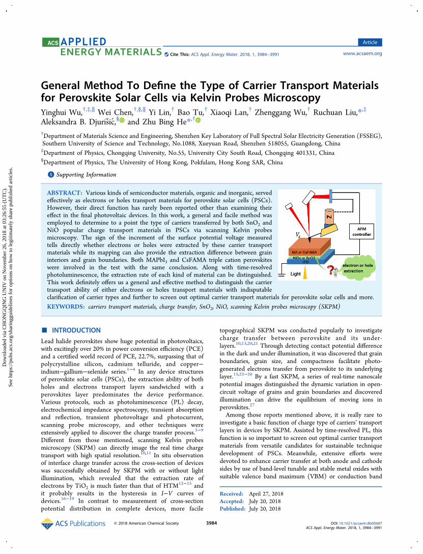
Figure 1. Topographic SEM images of MA perovskite films on SnO2/ITO glass (a) and on NiO/ITO glass (b); CsFAMA triple cations perovskitefilms on SnO2/ITO glass (c) and on NiO/ITO glass (d); cross-section SEM images of MA perovskite films on SnO2/ITO glass (e) and on NiO/ITO glass (f); CsFAMA triple cations perovskite films on SnO2/ITO glass (g) and on NiO/ITO glass (h). The scale bar is 1 μm for all images.
ACS Applied Energy Materials Article
DOI: 10.1021/acsaem.8b00687ACS Appl. Energy Mater. 2018, 1, 3984−3991
3985

5.67 eV in air environment, which also claims it is difficult to identifya definite dividing span of surface potential voltages measured. Thesurface of the sample in the test was grounded. Amplitude modulation(AM-) SKPM was adopted in this work and carried out in a two-passmanner, which has a merit of decoupling the signal of topography andsurface potential on orthogonal frequencies. The first pass is used todetermine the topography of the surface while the return trace is tomeasure the surface potential after lifting the probe at a slight height(below 50 nm) above the measured sample surface of the first trace.In the second process, raising the tip away from the surface eliminatescross-talk between topography and surface potential, while the closedistance between tip and surface enhances the lateral resolution ofelectrostatic forces, which is examined by our clear SKPM images inthe following text. An AC voltage (VACsin(ωt)) signal is applied toinduce a mechanical oscillation proportional to the tip−surfaceelectrostatic interaction strength, while a dynamic bucking DC voltage(VDC) added to the probe is in order to minimize the surface potentialdifference between tip and sample surface.
■ RESULTS AND DISSCUSSION
The SnO2 ETLs and NiO HTLs on cleaned ITO glasssubstrates were deposited with SnO2 and NiO nanoparticleinks at room temperature, respectively, according to previouslyreported procedure.35,38 A pinhole free SnO2 and NiO thinfilm with uniform tiny nanoparticles were shown in the surfaceimages of scanning electronic microscopy (SEM) and atomicforce microscopy (AFM) in Supporting Information FigureS1a−d. The phase images of Figure S1e,f confirm thecompactness of these two films. Similarly, two kinds ofp e r o v s k i t e s , M A P b I 3 ( M A ) a n d C s 0 . 0 5(FA0.85MA0.15)0.95PbBr0.15I0.85 (CsFAMA), were spin coatedon SnO2/ITO and NiO/ITO substrates, respectively.32,43 Bothkinds of perovskite films show high film crystallinity on thosesubstrates (Figure S2). Excess PbI2 signal was found in X-raydiffraction patterns of both CsFAMA films.37 Figure 1 showsthe surface morphologies of the perovskite films with highuniformity and compactness. For MA, the grain size of the filmon SnO2 is remarkably larger than that on NiO, which isconsistent with other reports.34,40 That may be attributed tosurface wettability variation between NiO and SnO2. Lowerwettability and crystallinity lead to larger grain size of theperovskite film.33,39,44−46 For CsFAMA, the grain size of bothfilms on NiO and SnO2 is smaller than that of MA. Moreover,excess PbI2 flakes turn up in grain boundaries obviously, whichis in accordance with our XRD patterns.38 Each correspondingcross-section scanning electronic microscopy (SEM) image(Figure 1e−h) was shown just below their topography, whichalso confirms high uniformity in thickness adequately in spiteof the resolution limit of our SEM tool. The thicknesses ofCsFAMA films on SnO2/NiO are around 500 and 515 nm,
respectively, while those of MA films on SnO2/NiO are around390 and 375 nm, respectively.The UV−vis absorption spectra of each perovskite film were
shown in Figure 2a,b. On SnO2 substrates (Figure 2a), theabsorption edge of CsFAMA has a noticeable red shiftcompared with that of MA on both substrates owing tobandgap shrinkage after alloying Cs and FA ions in thecompound, which is verified by the same shift from 772 to 786nm in their PL spectra, as the red lines show. It is similar forthe two kinds of perovskites on NiO substrates (Figure 2b). Itis interesting that there also is a slight red shift for bothperovskite films when changing the substrates from NiO toSnO2 (shown in Figure 2), which also is reported by formerliterature.31,41
To test the carrier extraction rate of SnO2 and NiO films,time-resolved PL (TRPL) was involved to distinguish thedifference between SnO2 and NiO for the two kinds ofperovskites. Figure 3a shows the PL of MA quenched by NiO
and SnO2 in contrast to the control bare ITO substrate,respectively. In comparison, NiO shows stronger carrierextraction ability than SnO2 although both of them are highlyeffective, as shown in the quenching extent in Figure 3a,b,which is confirmed by their TRPL results (Figure 3c). ForCsFAMA (Figure 3b,d), the PL quenching and TRPL abide bythe same law as MA, which further proves the differentia in
Figure 2. (a) Absorption and PL spectra of MA and CsFAMA films on SnO2/ITO glass; (b) MA and CsFAMA films on NiO/ITO glass.
Figure 3. PL spectra of (a) MA perovskite films and (b) CsFAMAperovskite films on ITO, SnO2/ITO, and NiO/ITO substrates,respectively; TRPL spectra of (c) MA perovskite films and (d)CsFAMA perovskite films on ITO, SnO2/ITO, and NiO/ITOsubstrates, respectively.
ACS Applied Energy Materials Article
DOI: 10.1021/acsaem.8b00687ACS Appl. Energy Mater. 2018, 1, 3984−3991
3986

carrier extraction ability of them. Regarding the PL decay ofeach sample, a biexponential decay I(t) = A1 exp(t/τ1) + A2exp(t/τ2) was used to identify the two stage decay time, andthe average lifetime can then be determined as τav = (∑iAiτi
2)/(∑i Aiτi).47 All the data were summarized in Table S1.
The first decay time (τ1) can reflect the monomolecularrecombination driven by defects while the second decay time(τ2) manifests the irradiative recombination of electron andhole photogenerated in perovskite films as its intrinsicproperty.47 Here, the so-called monomolecular recombinationcan be attributed mainly to electrons or holes only extractionby SnO2 and NiO, respectively. It is clearly shown that theweight of the first decay increases from near 2% to ca. 7.6% forboth SnO2 and NiO in the system of MA perovskites, whichobviously demonstrates the carrier extraction function of them(Table S1). In comparison, NiO’s extraction is much fasterthan that of SnO2 as τ1 decreases from 7.78 to 3.79 ns, whichdemonstrates clearly that the extraction rate of NiO isobviously higher than that of SnO2 (Table S1). The lifetimeof over 100 ns indicates good quality of MA perovskite filmswhile CsFAMA perovskite films also own near 200 ns inlifetime and show excellent quality. Although TRPL candiscover the extraction behavior and even compare carrierextraction ability between SnO2 and NiO, it is still impossiblefor TRPL to define the extracted carrier type by NiO or SnO2although they are deemed already as holes and electronstransport layers, respectively. However, SKPM affords thisfunction exactly.To eliminate test errors from environment and operation, all
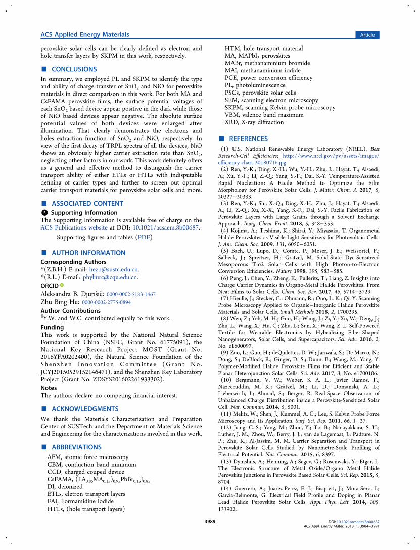
the SKPM measurements were conducted with one identicalprobe at 35% RH and 25 °C within 1 day. A dynamic buckingvoltage was used to eliminate the contact potential differencebetween the tip and the surface when encountering differentroughness surfaces.48−51 Before SKPM tests, topographic AFMmeasurements were carried out to reveal the surfacemorphology of each sample. The average roughness of MA/SnO2/ITO is 16.4 nm while that of CsFAMA/SnO2/ITO is23.3 nm shown in Figure 4a,d. The corresponding three-dimensional morphologies are also shown in Figure S3a,b,respectively. For the surface potential image of MA/SnO2/ITOin the dark (Figure 4b), grain interiors exhibit brightly with
slightly black grain boundary lines while the grains vary fromeach other. The grain size is so large and the film is so compactthat it blurs the surface potential difference between grains andgrain boundaries, although they are clearly distinguished in theimage. The brightness contrast from grain to grain can beattributed in some degree to height difference along withpossible difference in the crystallinity of each grain.7,18,52 Asdiscussed in those literature, the higher the grain crystallinity,the less the nonradiative recombination, faster the extractionrate, and larger the number of electrons or holes left. The finalresult is the higher brightness. In addition, although the returntrace thereotically eliminates the height difference recorded inthe first trace described in the working principle of SKPM, theabrupt contrast of grain height definitely inlfuences therecording of contact potential tracing the morphology, whichresults in the brightness contrast in an alternative way. Whenlight is on, the surface potential map varies except that somedeep valleys turn visually dark, as the white dashed line shows(Figure 4c). That seems interesting, and its underlyingmechanism remains unclear. The positive surface potential ofMA/SnO2/ITO indicates the possible electron extractioneffect of SnO2 by a depletion region at the interface of MA/SnO2 in the dark (Figure 4b). The surface potential voltage inthe scan region ranges from +130.01 to +172.95 mV in thedark while it is enlarged in its absolute value ranging from from+379.80 to +413.98 mV in the light. The area-mean intensityvaries from 155.89 to 398.78 mV by photogenerated electron−hole pairs after illumination (Figure 4c). After illumination,more carriers are generated by photons. The electrons amongthem will be extracted at the interface of perovskite/SnO2 bySnO2, and hence more holes in a balance state remain in theperovskite film and are induced by the SKPM tip. It results inhigher absolute values on average than that in the dark. Thepositive augmentation in surface potential voltage byillumination confirms the electron extraction ability of SnO2under the MA perovskite film. The similar phenomenon wasalso reported on TiO2 based MA perovskite films,15,22,53,54
although the values reported varied in different literature evenwith the same AFM probe, such as Pt/Ir or Au. Whatever, wecan attribute these positive values and illumination derivedaugmentations of surface potential voltages detected by SKPM
Figure 4. Topographic morphology image (a), dark-SKPM image (b), and light-SKPM image (c) of MA/SnO2/ITO glass; topographicmorphology image (d), dark-SKPM image (e), and light-SKPM image (f) of CsFAMA/SnO2/ITO glass. The scanning scales are 5 μm × 5 μm, andthe scale bars are 1 μm.
ACS Applied Energy Materials Article
DOI: 10.1021/acsaem.8b00687ACS Appl. Energy Mater. 2018, 1, 3984−3991
3987

to the electrons extraction ability of SnO2. In our work, thefunction of SnO2 is also fulfilled in the same way in CsFAMA/SnO2/ITO (Figure 4e,f). Compared to MA, the grain size ofCsFAMA film is much smaller and the roughness is larger,which exhibits a larger contrast in surface potential betweengrains and grain boundaries. That is more consistent with thephenomena that occurred in perovskite/TiO2.
23−26 Panels aand c of Figure S4 show the surface potential profiles extractedfrom the white dashed line shown in Figure 4a−c. Basically inthe profile, all the surface potentials both in dark and lightfollow the height change except for some misfits. The potentialcontrast between grains and grain boundaries attenuates afterillumination. A similar conclusion can be drawn from FigureS4b,d.In contrast to such an ambiguous explanation of charge
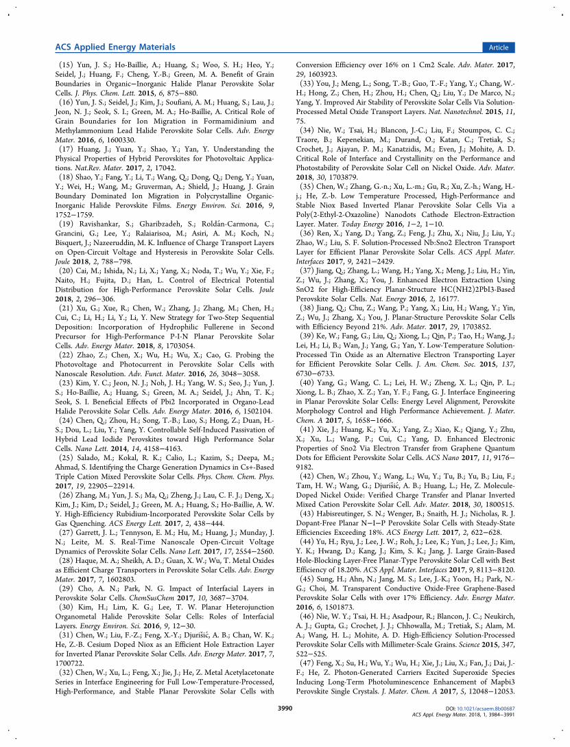
separation in perovskites/PEDOT:PSS,15 this work declaresthe explicit holes extraction behavior from perovskites to NiOHTLs, examined by SKPM again. Panels a and d of Figure 5show topographical images of MA and CsFAMA perovskitefilms deposited on NiO/ITO glass, and the area-meanroughness is around 14.3 and 20.7 nm, respectively. Thecorresponding three-dimensional surface morphologies wereexhibited in Figure S3c,d. Grains and grain boundaries areunambiguous in the surface potential image obtained in thedark (Figure 5b). Different from that of SnO2, most graininteriors appear darker than grain boundaries, which isattributed to the display habit of the vertical scale bar. Inthese SKPM images in Figure 5, the darker in color means thehigher in absolute value of surface potential voltage. It is clearlyshown that the absolute value of surface potential voltagebecomes larger after illumination, which demonstrates thatnew light driven electrons are accumulated at the surface byextracting holes via NiO when the sample is detected by theSKPM probe (Figure 5b,c). This phenomenon has also beendetected in the former reports,53,55,56 where most of thesurface potential voltage values became more negative afterillumination. However, it is really difficult to determine anaccurate dividing span of surface potential voltages to tellwhich span definitely indexed to a net positive or negativeregion, because the measured values varied by AFM systems,the work function of SKPM probe materials, and even differentsynthesis conditions of the samples. In the NiO based devices
of our work, for MA perovskite, the surface potential voltageranged from −288.10 to −348.17 mV in the scan region, whichwas enlarged in a span (−327.16 to −395.31 mV) afterillumination. This phenomenon was also reported in theperovskite devices with PEDOT:PSS as hole transportlayer.53,55 For CsFAMA, the value spans detected in darkand in light are from −224.13 to −266.06 mV and from−310.94 to −354.29 mV, respectively. After illumination, thearea-mean surface potential voltage of CsFAMA/NiO/ITOwas enhanced obviously from −240.86 to −329.32 mV, wherethe absolute value augmentation after illumination is alsodefinite. It should be also clarified here that this law standsalone from such features of perovskite films as thickness, grainsize, and even morphology, although those factors possiblymodify the absolute values within a range, as discussed in someliterature.22,57
Here, we summarize the surface potential voltages detectedby SKPM protocols from both our works and the formerreports (Table S1) and draw a firm conclusion that the SnO2ETL series lead to the positive augmentation of the surfacepotential voltage while the NiO HTL series lead to thenegative increment of that. Herein, the electron or holeextraction ability of these transport materials is responsible forthe positive or negative increment of the surface potentialvoltage detected by SKPM. Although the surface portentialvoltage values of the SnO2 based perovskite devices areobviously positive while those of the NiO based are clearlynegative in our work, it is not yet easy to define the accuratedividing span for different AFM systems, different probes andenvironments, and even objects synthesized by different routes.Beyond any questions, the extracted carrier type can bediscriminated by the sign of the increment of the surfacepotential voltage.Moreover, the surface potential profiles (Figure S5a,b)
extracted from the white dashed lines in Figure 5b,c;e,f alsofollow the corresponding height traces to a large extent, alongwith some little discrepancies (Figure S5c,d). The underlyingmechanism still needs further exploring. However, regardless ofthe difference in the images and profiles, the negative surfacepotential values demonstrate the indisputable holes extractionfunction of NiO. The area-mean surface potential variation wassummarized in Table S2. The actual role of SnO2 and NiO for
Figure 5. Topographic morphology image (a), dark-SKPM image (b), and light-SKPM image (c) of MA/NiO/ITO glass; topographic morphologyimage (d), dark-SKPM image (e), and light-SKPM image (f) of CsFAMA/NiO/ITO glass. The scanning scales are 5 μm × 5 μm, and the scale barsare 1 μm.
ACS Applied Energy Materials Article
DOI: 10.1021/acsaem.8b00687ACS Appl. Energy Mater. 2018, 1, 3984−3991
3988
perovskite solar cells can be clearly defined as electron andhole transfer layers by SKPM in this work, respectively.
■ CONCLUSIONSIn summary, we employed PL and SKPM to identify the typeand ability of charge transfer of SnO2 and NiO for perovskitematerials in direct comparison in this work. For both MA andCsFAMA perovskite films, the surface potential voltages ofeach SnO2 based device appear positive in the dark while thoseof NiO based devices appear negative. The absolute surfacepotential values of both devices were enlarged afterillumination. That clearly demonstrates the electrons andholes extraction function of SnO2 and NiO, respectively. Inview of the first decay of TRPL spectra of all the devices, NiOshows an obviously higher carrier extraction rate than SnO2,neglecting other factors in our work. This work definitely offersus a general and effective method to distinguish the carriertransport ability of either ETLs or HTLs with indisputabledefining of carrier types and further to screen out optimalcarrier transport materials for perovskite solar cells and more.
■ ASSOCIATED CONTENT*S Supporting InformationThe Supporting Information is available free of charge on theACS Publications website at DOI: 10.1021/acsaem.8b00687.
Supporting figures and tables (PDF)
■ AUTHOR INFORMATIONCorresponding Authors*(Z.B.H.) E-mail: [email protected].*(R.L.) E-mail: [email protected] B. Djurisic: 0000-0002-5183-1467Zhu Bing He: 0000-0002-2775-0894Author Contributions∥Y.W. and W.C. contributed equally to this work.FundingThis work is supported by the National Natural ScienceFoundation of China (NSFC; Grant No. 61775091), theNational Key Research Project MOST (Grant No.2016YFA0202400), the Natural Science Foundation of theShen zhen Innov a t i on Commi t t e e (Gr an t No .JCYJ20150529152146471), and the Shenzhen Key LaboratoryProject (Grant No. ZDSYS201602261933302).NotesThe authors declare no competing financial interest.
■ ACKNOWLEDGMENTSWe thank the Materials Characterization and PreparationCenter of SUSTech and the Department of Materials Scienceand Engineering for the characterizations involved in this work.
■ ABBREVIATIONSAFM, atomic force microscopyCBM, conduction band minimumCCD, charged couped deviceCsFAMA, (FA0.85MA0.15)0.95PbBr0.15I0.85DI, deionizedETLs, eletron transport layersFAI, Formamidine iodideHTLs, (hole transport layers)
HTM, hole transport materialMA, MAPbI3 perovskitesMABr, methanaminium bromideMAI, methanaminium iodidePCE, power conversion efficiencyPL, photoluminescencePSCs, perovskite solar cellsSEM, scanning electron microscopySKPM, scanning Kelvin probe microscopyVBM, valence band maximumXRD, X-ray diffraction
■ REFERENCES(1) U.S. National Renewable Energy Laboratory (NREL). BestResearch-Cell Efficiencies; http://www.nrel.gov/pv/assets/images/efficiency-chart-20180716.jpg.(2) Ren, Y.-K.; Ding, X.-H.; Wu, Y.-H.; Zhu, J.; Hayat, T.; Alsaedi,A.; Xu, Y.-F.; Li, Z.-Q.; Yang, S.-F.; Dai, S.-Y. Temperature-AssistedRapid Nucleation: A Facile Method to Optimize the FilmMorphology for Perovskite Solar Cells. J. Mater. Chem. A 2017, 5,20327−20333.(3) Ren, Y.-K.; Shi, X.-Q.; Ding, X.-H.; Zhu, J.; Hayat, T.; Alsaedi,A.; Li, Z.-Q.; Xu, X.-X.; Yang, S.-F.; Dai, S.-Y. Facile Fabrication ofPerovskite Layers with Large Grains through a Solvent ExchangeApproach. Inorg. Chem. Front. 2018, 5, 348−353.(4) Kojima, A.; Teshima, K.; Shirai, Y.; Miyasaka, T. OrganometalHalide Perovskites as Visible-Light Sensitizers for Photovoltaic Cells.J. Am. Chem. Soc. 2009, 131, 6050−6051.(5) Bach, U.; Lupo, D.; Comte, P.; Moser, J. E.; Weissortel, F.;Salbeck, J.; Spreitzer, H.; Gratzel, M. Solid-State Dye-SensitizedMesoporous Tio2 Solar Cells with High Photon-to-ElectronConversion Efficiencies. Nature 1998, 395, 583−585.(6) Peng, J.; Chen, Y.; Zheng, K.; Pullerits, T.; Liang, Z. Insights intoCharge Carrier Dynamics in Organo-Metal Halide Perovskites: FromNeat Films to Solar Cells. Chem. Soc. Rev. 2017, 46, 5714−5729.(7) Hieulle, J.; Stecker, C.; Ohmann, R.; Ono, L. K.; Qi, Y. ScanningProbe Microscopy Applied to Organic−Inorganic Halide PerovskiteMaterials and Solar Cells. Small Methods 2018, 2, 1700295.(8) Wen, Z.; Yeh, M.-H.; Guo, H.; Wang, J.; Zi, Y.; Xu, W.; Deng, J.;Zhu, L.; Wang, X.; Hu, C.; Zhu, L.; Sun, X.; Wang, Z. L. Self-PoweredTextile for Wearable Electronics by Hybridizing Fiber-ShapedNanogenerators, Solar Cells, and Supercapacitors. Sci. Adv. 2016, 2,No. e1600097.(9) Zuo, L.; Guo, H.; deQuilettes, D. W.; Jariwala, S.; De Marco, N.;Dong, S.; DeBlock, R.; Ginger, D. S.; Dunn, B.; Wang, M.; Yang, Y.Polymer-Modified Halide Perovskite Films for Efficient and StablePlanar Heterojunction Solar Cells. Sci. Adv. 2017, 3, No. e1700106.(10) Bergmann, V. W.; Weber, S. A. L.; Javier Ramos, F.;Nazeeruddin, M. K.; Gra tzel, M.; Li, D.; Domanski, A. L.;Lieberwirth, I.; Ahmad, S.; Berger, R. Real-Space Observation ofUnbalanced Charge Distribution inside a Perovskite-Sensitized SolarCell. Nat. Commun. 2014, 5, 5001.(11) Melitz, W.; Shen, J.; Kummel, A. C.; Lee, S. Kelvin Probe ForceMicroscopy and Its Application. Surf. Sci. Rep. 2011, 66, 1−27.(12) Jiang, C.-S.; Yang, M.; Zhou, Y.; To, B.; Nanayakkara, S. U.;Luther, J. M.; Zhou, W.; Berry, J. J.; van de Lagemaat, J.; Padture, N.P.; Zhu, K.; Al-Jassim, M. M. Carrier Separation and Transport inPerovskite Solar Cells Studied by Nanometre-Scale Profiling ofElectrical Potential. Nat. Commun. 2015, 6, 8397.(13) Dymshits, A.; Henning, A.; Segev, G.; Rosenwaks, Y.; Etgar, L.The Electronic Structure of Metal Oxide/Organo Metal HalidePerovskite Junctions in Perovskite Based Solar Cells. Sci. Rep. 2015, 5,8704.(14) Guerrero, A.; Juarez-Perez, E. J.; Bisquert, J.; Mora-Sero, I.;Garcia-Belmonte, G. Electrical Field Profile and Doping in PlanarLead Halide Perovskite Solar Cells. Appl. Phys. Lett. 2014, 105,133902.
ACS Applied Energy Materials Article
DOI: 10.1021/acsaem.8b00687ACS Appl. Energy Mater. 2018, 1, 3984−3991
3989
(15) Yun, J. S.; Ho-Baillie, A.; Huang, S.; Woo, S. H.; Heo, Y.;Seidel, J.; Huang, F.; Cheng, Y.-B.; Green, M. A. Benefit of GrainBoundaries in Organic−Inorganic Halide Planar Perovskite SolarCells. J. Phys. Chem. Lett. 2015, 6, 875−880.(16) Yun, J. S.; Seidel, J.; Kim, J.; Soufiani, A. M.; Huang, S.; Lau, J.;Jeon, N. J.; Seok, S. I.; Green, M. A.; Ho-Baillie, A. Critical Role ofGrain Boundaries for Ion Migration in Formamidinium andMethylammonium Lead Halide Perovskite Solar Cells. Adv. EnergyMater. 2016, 6, 1600330.(17) Huang, J.; Yuan, Y.; Shao, Y.; Yan, Y. Understanding thePhysical Properties of Hybrid Perovskites for Photovoltaic Applica-tions. Nat.Rev. Mater. 2017, 2, 17042.(18) Shao, Y.; Fang, Y.; Li, T.; Wang, Q.; Dong, Q.; Deng, Y.; Yuan,Y.; Wei, H.; Wang, M.; Gruverman, A.; Shield, J.; Huang, J. GrainBoundary Dominated Ion Migration in Polycrystalline Organic-Inorganic Halide Perovskite Films. Energy Environ. Sci. 2016, 9,1752−1759.(19) Ravishankar, S.; Gharibzadeh, S.; Roldan-Carmona, C.;Grancini, G.; Lee, Y.; Ralaiarisoa, M.; Asiri, A. M.; Koch, N.;Bisquert, J.; Nazeeruddin, M. K. Influence of Charge Transport Layerson Open-Circuit Voltage and Hysteresis in Perovskite Solar Cells.Joule 2018, 2, 788−798.(20) Cai, M.; Ishida, N.; Li, X.; Yang, X.; Noda, T.; Wu, Y.; Xie, F.;Naito, H.; Fujita, D.; Han, L. Control of Electrical PotentialDistribution for High-Performance Perovskite Solar Cells. Joule2018, 2, 296−306.(21) Xu, G.; Xue, R.; Chen, W.; Zhang, J.; Zhang, M.; Chen, H.;Cui, C.; Li, H.; Li, Y.; Li, Y. New Strategy for Two-Step SequentialDeposition: Incorporation of Hydrophilic Fullerene in SecondPrecursor for High-Performance P-I-N Planar Perovskite SolarCells. Adv. Energy Mater. 2018, 8, 1703054.(22) Zhao, Z.; Chen, X.; Wu, H.; Wu, X.; Cao, G. Probing thePhotovoltage and Photocurrent in Perovskite Solar Cells withNanoscale Resolution. Adv. Funct. Mater. 2016, 26, 3048−3058.(23) Kim, Y. C.; Jeon, N. J.; Noh, J. H.; Yang, W. S.; Seo, J.; Yun, J.S.; Ho-Baillie, A.; Huang, S.; Green, M. A.; Seidel, J.; Ahn, T. K.;Seok, S. I. Beneficial Effects of Pbi2 Incorporated in Organo-LeadHalide Perovskite Solar Cells. Adv. Energy Mater. 2016, 6, 1502104.(24) Chen, Q.; Zhou, H.; Song, T.-B.; Luo, S.; Hong, Z.; Duan, H.-S.; Dou, L.; Liu, Y.; Yang, Y. Controllable Self-Induced Passivation ofHybrid Lead Iodide Perovskites toward High Performance SolarCells. Nano Lett. 2014, 14, 4158−4163.(25) Salado, M.; Kokal, R. K.; Calio, L.; Kazim, S.; Deepa, M.;Ahmad, S. Identifying the Charge Generation Dynamics in Cs+-BasedTriple Cation Mixed Perovskite Solar Cells. Phys. Chem. Chem. Phys.2017, 19, 22905−22914.(26) Zhang, M.; Yun, J. S.; Ma, Q.; Zheng, J.; Lau, C. F. J.; Deng, X.;Kim, J.; Kim, D.; Seidel, J.; Green, M. A.; Huang, S.; Ho-Baillie, A. W.Y. High-Efficiency Rubidium-Incorporated Perovskite Solar Cells byGas Quenching. ACS Energy Lett. 2017, 2, 438−444.(27) Garrett, J. L.; Tennyson, E. M.; Hu, M.; Huang, J.; Munday, J.N.; Leite, M. S. Real-Time Nanoscale Open-Circuit VoltageDynamics of Perovskite Solar Cells. Nano Lett. 2017, 17, 2554−2560.(28) Haque, M. A.; Sheikh, A. D.; Guan, X. W.; Wu, T. Metal Oxidesas Efficient Charge Transporters in Perovskite Solar Cells. Adv. EnergyMater. 2017, 7, 1602803.(29) Cho, A. N.; Park, N. G. Impact of Interfacial Layers inPerovskite Solar Cells. ChemSusChem 2017, 10, 3687−3704.(30) Kim, H.; Lim, K. G.; Lee, T. W. Planar HeterojunctionOrganometal Halide Perovskite Solar Cells: Roles of InterfacialLayers. Energy Environ. Sci. 2016, 9, 12−30.(31) Chen, W.; Liu, F.-Z.; Feng, X.-Y.; Djurisic, A. B.; Chan, W. K.;He, Z.-B. Cesium Doped Niox as an Efficient Hole Extraction Layerfor Inverted Planar Perovskite Solar Cells. Adv. Energy Mater. 2017, 7,1700722.(32) Chen, W.; Xu, L.; Feng, X.; Jie, J.; He, Z. Metal AcetylacetonateSeries in Interface Engineering for Full Low-Temperature-Processed,High-Performance, and Stable Planar Perovskite Solar Cells with
Conversion Efficiency over 16% on 1 Cm2 Scale. Adv. Mater. 2017,29, 1603923.(33) You, J.; Meng, L.; Song, T.-B.; Guo, T.-F.; Yang, Y.; Chang, W.-H.; Hong, Z.; Chen, H.; Zhou, H.; Chen, Q.; Liu, Y.; De Marco, N.;Yang, Y. Improved Air Stability of Perovskite Solar Cells Via Solution-Processed Metal Oxide Transport Layers. Nat. Nanotechnol. 2015, 11,75.(34) Nie, W.; Tsai, H.; Blancon, J.-C.; Liu, F.; Stoumpos, C. C.;Traore, B.; Kepenekian, M.; Durand, O.; Katan, C.; Tretiak, S.;Crochet, J.; Ajayan, P. M.; Kanatzidis, M.; Even, J.; Mohite, A. D.Critical Role of Interface and Crystallinity on the Performance andPhotostability of Perovskite Solar Cell on Nickel Oxide. Adv. Mater.2018, 30, 1703879.(35) Chen, W.; Zhang, G.-n.; Xu, L.-m.; Gu, R.; Xu, Z.-h.; Wang, H.-j.; He, Z.-b. Low Temperature Processed, High-Performance andStable Niox Based Inverted Planar Perovskite Solar Cells Via aPoly(2-Ethyl-2-Oxazoline) Nanodots Cathode Electron-ExtractionLayer. Mater. Today Energy 2016, 1−2, 1−10.(36) Ren, X.; Yang, D.; Yang, Z.; Feng, J.; Zhu, X.; Niu, J.; Liu, Y.;Zhao, W.; Liu, S. F. Solution-Processed Nb:Sno2 Electron TransportLayer for Efficient Planar Perovskite Solar Cells. ACS Appl. Mater.Interfaces 2017, 9, 2421−2429.(37) Jiang, Q.; Zhang, L.; Wang, H.; Yang, X.; Meng, J.; Liu, H.; Yin,Z.; Wu, J.; Zhang, X.; You, J. Enhanced Electron Extraction UsingSnO2 for High-Efficiency Planar-Structure HC(NH2)2PbI3-BasedPerovskite Solar Cells. Nat. Energy 2016, 2, 16177.(38) Jiang, Q.; Chu, Z.; Wang, P.; Yang, X.; Liu, H.; Wang, Y.; Yin,Z.; Wu, J.; Zhang, X.; You, J. Planar-Structure Perovskite Solar Cellswith Efficiency Beyond 21%. Adv. Mater. 2017, 29, 1703852.(39) Ke, W.; Fang, G.; Liu, Q.; Xiong, L.; Qin, P.; Tao, H.; Wang, J.;Lei, H.; Li, B.; Wan, J.; Yang, G.; Yan, Y. Low-Temperature Solution-Processed Tin Oxide as an Alternative Electron Transporting Layerfor Efficient Perovskite Solar Cells. J. Am. Chem. Soc. 2015, 137,6730−6733.(40) Yang, G.; Wang, C. L.; Lei, H. W.; Zheng, X. L.; Qin, P. L.;Xiong, L. B.; Zhao, X. Z.; Yan, Y. F.; Fang, G. J. Interface Engineeringin Planar Perovskite Solar Cells: Energy Level Alignment, PerovskiteMorphology Control and High Performance Achievement. J. Mater.Chem. A 2017, 5, 1658−1666.(41) Xie, J.; Huang, K.; Yu, X.; Yang, Z.; Xiao, K.; Qiang, Y.; Zhu,X.; Xu, L.; Wang, P.; Cui, C.; Yang, D. Enhanced ElectronicProperties of Sno2 Via Electron Transfer from Graphene QuantumDots for Efficient Perovskite Solar Cells. ACS Nano 2017, 11, 9176−9182.(42) Chen, W.; Zhou, Y.; Wang, L.; Wu, Y.; Tu, B.; Yu, B.; Liu, F.;Tam, H. W.; Wang, G.; Djurisic, A. B.; Huang, L.; He, Z. Molecule-Doped Nickel Oxide: Verified Charge Transfer and Planar InvertedMixed Cation Perovskite Solar Cell. Adv. Mater. 2018, 30, 1800515.(43) Habisreutinger, S. N.; Wenger, B.; Snaith, H. J.; Nicholas, R. J.Dopant-Free Planar N−I−P Perovskite Solar Cells with Steady-StateEfficiencies Exceeding 18%. ACS Energy Lett. 2017, 2, 622−628.(44) Yu, H.; Ryu, J.; Lee, J. W.; Roh, J.; Lee, K.; Yun, J.; Lee, J.; Kim,Y. K.; Hwang, D.; Kang, J.; Kim, S. K.; Jang, J. Large Grain-BasedHole-Blocking Layer-Free Planar-Type Perovskite Solar Cell with BestEfficiency of 18.20%. ACS Appl. Mater. Interfaces 2017, 9, 8113−8120.(45) Sung, H.; Ahn, N.; Jang, M. S.; Lee, J.-K.; Yoon, H.; Park, N.-G.; Choi, M. Transparent Conductive Oxide-Free Graphene-BasedPerovskite Solar Cells with over 17% Efficiency. Adv. Energy Mater.2016, 6, 1501873.(46) Nie, W. Y.; Tsai, H. H.; Asadpour, R.; Blancon, J. C.; Neukirch,A. J.; Gupta, G.; Crochet, J. J.; Chhowalla, M.; Tretiak, S.; Alam, M.A.; Wang, H. L.; Mohite, A. D. High-Efficiency Solution-ProcessedPerovskite Solar Cells with Millimeter-Scale Grains. Science 2015, 347,522−525.(47) Feng, X.; Su, H.; Wu, Y.; Wu, H.; Xie, J.; Liu, X.; Fan, J.; Dai, J.-F.; He, Z. Photon-Generated Carriers Excited Superoxide SpeciesInducing Long-Term Photoluminescence Enhancement of Mapbi3Perovskite Single Crystals. J. Mater. Chem. A 2017, 5, 12048−12053.
ACS Applied Energy Materials Article
DOI: 10.1021/acsaem.8b00687ACS Appl. Energy Mater. 2018, 1, 3984−3991
3990

(48) Nonnenmacher, M.; O'Boyle, M. P.; Wickramasinghe, H. K.Kelvin Probe Force Microscopy. Appl. Phys. Lett. 1991, 58, 2921−2923.(49) Nonnenmacher, M.; O'Boyle, M.; Wickramasinghe, H. K.Surface Investigations with a Kelvin Probe Force Microscope.Ultramicroscopy 1992, 42-44, 268−273.(50) Lin, S.-q.; Shao, T.-m. Charge Erasure Analysis on theNanoscale Using Kelvin Probe Force Microscopy. AIP Adv. 2017, 7,075104.(51) Moores, B.; Hane, F.; Eng, L.; Leonenko, Z. Kelvin ProbeForce Microscopy in Application to Biomolecular Films: FrequencyModulation, Amplitude Modulation, and Lift Mode. Ultramicroscopy2010, 110, 708−711.(52) Rothmann, M. U.; Li, W.; Etheridge, J.; Cheng, Y.-B.Microstructural Characterisations of Perovskite Solar Cells − fromGrains to Interfaces: Techniques, Features, and Challenges. Adv.Energy Mater. 2017, 7, 1700912.(53) Li, J.-J.; Ma, J.-Y.; Ge, Q.-Q.; Hu, J.-S.; Wang, D.; Wan, L.-J.Microscopic Investigation of Grain Boundaries in Organolead HalidePerovskite Solar Cells. ACS Appl. Mater. Interfaces 2015, 7, 28518−28523.(54) Li, J.-J.; Ma, J.-Y.; Hu, J.-S.; Wang, D.; Wan, L.-J. Influence ofN,N-Dimethylformamide Annealing on the Local Electrical Propertiesof Organometal Halide Perovskite Solar Cells: An Atomic ForceMicroscopy Investigation. ACS Appl. Mater. Interfaces 2016, 8,26002−26007.(55) Chang, J.; Zhu, H.; Xiao, J.; Isikgor, F. H.; Lin, Z.; Hao, Y.;Zeng, K.; Xu, Q.-H.; Ouyang, J. Enhancing the Planar HeterojunctionPerovskite Solar Cell Performance through Tuning the PrecursorRatio. J. Mater. Chem. A 2016, 4, 7943−7949.(56) Chiesa, M.; Burgi, L.; Kim, J. S.; Shikler, R.; Friend, R. H.;Sirringhaus, H. Correlation between Surface Photovoltage and BlendMorphology in Polyfluorene-Based Photodiodes. Nano Lett. 2005, 5,559−563.(57) Adhikari, N.; Dubey, A.; Khatiwada, D.; Mitul, A. F.; Wang, Q.;Venkatesan, S.; Iefanova, A.; Zai, J.; Qian, X.; Kumar, M.; Qiao, Q.Interfacial Study to Suppress Charge Carrier Recombination for HighEfficiency Perovskite Solar Cells. ACS Appl. Mater. Interfaces 2015, 7,26445−26454.
ACS Applied Energy Materials Article
DOI: 10.1021/acsaem.8b00687ACS Appl. Energy Mater. 2018, 1, 3984−3991
3991