GENERAL DESCRIPTION FEATURES...MC3419 3-Axis Accelerometer Preliminary Datasheet mCube Proprietary....
80
MC3419 3-Axis Accelerometer Preliminary Datasheet mCube Proprietary. APS-048-0071v1.01 1 / 80 © 2019 mCube Inc. All rights reserved. GENERAL DESCRIPTION The MC3419 is a small form factor, integrated digital output 3-axis accelerometer with a feature set optimized for cell phones and consumer product motion sensing. Applications include user interface control, gaming motion input, electronic compass tilt compensation for cell phones, game controllers, remote controls and portable media products. The MC3419 features a dedicated motion block which implements algorithms to support “any motion” and shake detection, tilt/flip and tilt 35 position detection. Low power consumption and small size are inherent in the monolithic fabrication approach, where the MEMS accelerometer is integrated in a single-chip with the electronics integrated circuit. In the MC3419 the internal sample rate can be set from 0.5 to 1000 samples / second. The device supports the reading of sample and event status via polling or interrupts. FEATURES Range, Sampling & Power • ±2, ±4, ±8, ±12, ±16g range • 16-bit single sample resolution • 16-bit resolution with FIFO • 0.5 to 1000 Hz Output Data Rate • 4 μA typical Standby current • Low typical active current Simple System Integration • SPI, up to 10 MHz • I2C interface, up to 1 MHz • 2×2×0.92 mm 12-pin LGA package • High reliability thru single-chip 3D silicon MEMS technology • RoHS compliant Applications • Smartphone • Wearable • IoT & IoMT • Remote controls, gaming • Vibration in Cell phone • VR & game controllers
Transcript of GENERAL DESCRIPTION FEATURES...MC3419 3-Axis Accelerometer Preliminary Datasheet mCube Proprietary....

MC3419 3-Axis Accelerometer Preliminary Datasheet
mCube Proprietary. APS-048-0071v1.01 1 / 80 © 2019 mCube Inc. All rights reserved.
GENERAL DESCRIPTION
The MC3419 is a small form factor, integrated digital output 3-axis accelerometer with a feature set optimized for cell phones and consumer product motion sensing. Applications include user interface control, gaming motion input, electronic compass tilt compensation for cell phones, game controllers, remote controls and portable media products.
The MC3419 features a dedicated motion block which implements algorithms to support “any motion” and shake detection, tilt/flip and tilt 35 position detection.
Low power consumption and small size are inherent in the monolithic fabrication approach, where the MEMS accelerometer is integrated in a single-chip with the electronics integrated circuit.
In the MC3419 the internal sample rate can be set from 0.5 to 1000 samples / second. The device supports the reading of sample and event status via polling or interrupts.
FEATURES
Range, Sampling & Power
• ±2, ±4, ±8, ±12, ±16g range • 16-bit single sample resolution • 16-bit resolution with FIFO • 0.5 to 1000 Hz Output Data Rate • 4 μA typical Standby current • Low typical active current
Simple System Integration
• SPI, up to 10 MHz • I2C interface, up to 1 MHz • 2×2×0.92 mm 12-pin LGA package • High reliability thru single-chip 3D
silicon MEMS technology • RoHS compliant
Applications
• Smartphone • Wearable • IoT & IoMT • Remote controls, gaming • Vibration in Cell phone • VR & game controllers
MC3419 3-Axis Accelerometer
mCube Proprietary. APS-048-0071v1.01 2 / 80 © 2019 mCube Inc. All rights reserved.
TABLE OF CONTENTS 1 Order Information ............................................................................................................. 5
2 Functional Block Diagram ................................................................................................ 6
3 Packaging and Pin Description ........................................................................................ 7
3.1 Package Outline ................................................................................................................... 7
3.2 Package Orientation ............................................................................................................. 8
3.3 Pin Description ..................................................................................................................... 9
3.4 Typical Application Circuits ................................................................................................ 10
3.5 Tape and Reel ................................................................................................................... 13
3.6 Soldering Profile ................................................................................................................. 15
3.7 Shipping and Handling Guidelines ..................................................................................... 15
3.8 Moisture Sensitivity Level Control ...................................................................................... 15
4 Specifications ................................................................................................................. 16
4.1 Absolute Maximum Ratings ................................................................................................ 16
4.2 Sensor Characteristics ....................................................................................................... 17
4.3 Electrical and Timing Characteristics .................................................................................. 18
4.3.1 Electrical Power and Internal Characteristics .................................................................. 18
4.3.2 Electrical Characteristics ................................................................................................ 19
4.3.3 I2C Timing Characteristics .............................................................................................. 20
5 General Operation ......................................................................................................... 21
5.1 Sensor Sampling ................................................................................................................ 21
5.2 Offset and Gain Calibration ................................................................................................ 21
6 Operational States ......................................................................................................... 22
7 Operational State Flow .................................................................................................. 23
8 Interrupts ........................................................................................................................ 24
8.1 Interrupt Overview .............................................................................................................. 24
8.2 Enabling and Clearing Interrupts ........................................................................................ 25
8.3 Interrupt Sources ................................................................................................................ 25
8.3.1 ACQ_INT Interrupt .......................................................................................................... 25
8.3.2 TILT/FLIP (TILT_INT, FLIP_INT) .................................................................................... 25
8.3.3 Interrupt on AnyMotion (ANYM_INT) .............................................................................. 25
8.3.4 Interrupt on SHAKE (SHAKE_INT) ................................................................................. 25
8.3.5 Interrupt on TILT_35 (TILT_35_INT) ............................................................................... 26
MC3419 3-Axis Accelerometer
mCube Proprietary. APS-048-0071v1.01 3 / 80 © 2019 mCube Inc. All rights reserved.
8.3.6 Interrupt on FIFO Empty (FIFO_EMPTY_INT) ................................................................ 26
8.3.7 Interrupt on FIFO Full (FIFO_FULL_INT) ........................................................................ 26
8.3.8 Interrupt on FIFO Threshold (FIFO_THRESH_INT) ........................................................ 26
8.4 Interrupt Servicing .............................................................................................................. 27
8.4.1 Global Interrupt Service Mode ........................................................................................ 27
8.4.2 Bitmask/Individual Interrupt Service Mode ...................................................................... 27
8.5 Interrupt Requests and External INT Pins .......................................................................... 29
8.5.1 Selecting Drive and Polarity ............................................................................................ 29
8.5.2 Swapping INT Pins ......................................................................................................... 30
8.5.3 Combining Interrupt Requests ........................................................................................ 30
9 Sampling ........................................................................................................................ 31
9.1 Continuous Sampling ......................................................................................................... 31
9.2 Setting the Sample Rate .................................................................................................... 31
9.3 Additional Rate Options ...................................................................................................... 32
10 I2C Interface .................................................................................................................. 33
10.1 Physical Interface ............................................................................................................... 33
10.2 Timing ................................................................................................................................ 34
10.3 I2C Message Format .......................................................................................................... 34
10.4 I2C Watchdog Timer .......................................................................................................... 35
10.5 SPI Physical Interface ........................................................................................................ 36
10.6 SPI Protocol ....................................................................................................................... 36
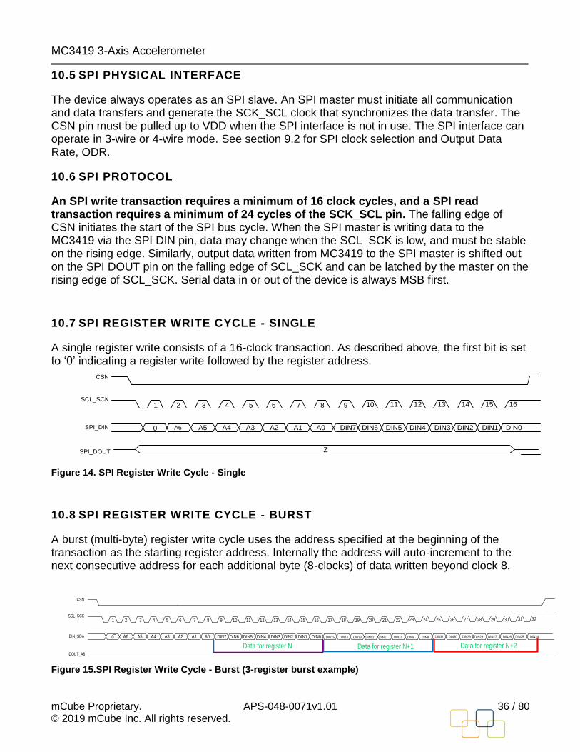
10.7 SPI Register Write Cycle - Single ....................................................................................... 36
10.8 SPI Register Write Cycle - Burst ........................................................................................ 36
10.9 SPI Register Read Cycle - Single ....................................................................................... 37
10.10 SPI Register Read Cycle - Burst ........................................................................................ 37
11 Register Interface .......................................................................................................... 38
11.1 Register Summary ............................................................................................................. 38
(0x05) ................................................................................................................................. 41
11.2 Device Status Register ....................................................................................................... 41
(0x06) ................................................................................................................................. 42
11.3 Interrupt Enable Register ................................................................................................... 42
11.4 (0x07) Mode Register ......................................................................................................... 43
11.5 (0x08) Sample Rate Register ............................................................................................. 44
11.6 (0x09) Motion Control Register ........................................................................................... 45
11.7 (0x0A) FIFO Status Register .............................................................................................. 46
MC3419 3-Axis Accelerometer
mCube Proprietary. APS-048-0071v1.01 4 / 80 © 2019 mCube Inc. All rights reserved.
11.8 (0x0B) FIFO Read Pointer Register .................................................................................... 47
11.9 (0x0C) FIFO Write Pointer Register .................................................................................... 48
11.10 (0x0D - 0x12) XOUT, YOUT and ZOUT Data Accelerometer Registers ............................. 49
11.11 (0x13) Status Register........................................................................................................ 50
11.12 (0x14) Interrupt Status Register ......................................................................................... 51
11.13 (0x20) Range and Scale Control Register .......................................................................... 53
11.14 (0x21 – 0x22) X-Axis Digital Offset Registers ..................................................................... 54
11.15 (0x23 – 0x24) Y-Axis Digital Offset Registers ..................................................................... 55
11.16 (0x25 – 0x26) Z-Axis Digital Offset Registers ..................................................................... 56
11.17 (0x22 & 0x27) X-Axis Digital Gain Registers ...................................................................... 57
11.18 (0x24 & 0x28) Y-Axis Digital Gain Registers ...................................................................... 58
11.19 (0x26 & 0x29) Z-Axis Digital Gain Registers ....................................................................... 59
11.20 (0x2D) FIFO Control Register ............................................................................................. 60
11.21 (0x2E) FIFO Threshold Register ........................................................................................ 62
11.22 (0x2F) FIFO Interrupt Status Register ................................................................................ 63
11.23 (0x30) FIFO Control Register2, Sample Rate Register 2 .................................................... 64
11.24 (0x31) Communication Control Register ............................................................................. 66
11.25 (0x33) GPIO Control Register ............................................................................................ 67
11.26 (0x40 – 0x41) Tilt/Flip Threshold Registers ........................................................................ 69
11.27 (0x42) Tilt/Flip Debounce Register ..................................................................................... 70
11.28 (0x43 – 0x44) AnyMotion Threshold Registers ................................................................... 71
11.29 (0x45) AnyMotion Debounce Register ................................................................................ 72
11.30 (0x46 – 0x47) Shake Threshold Registers.......................................................................... 73
11.31 (0x48 – 0x49) Shake Duration, Peak-to-Peak Registers ..................................................... 74
11.32 (0x4A) Timer Control Register ............................................................................................ 75
11.33 (0x4B) Read Count Register .............................................................................................. 76
12 Index of Tables .............................................................................................................. 77
13 Revision History ............................................................................................................. 79
14 Legal .............................................................................................................................. 80
MC3419 3-Axis Accelerometer
mCube Proprietary. APS-048-0071v1.01 5 / 80 © 2019 mCube Inc. All rights reserved.
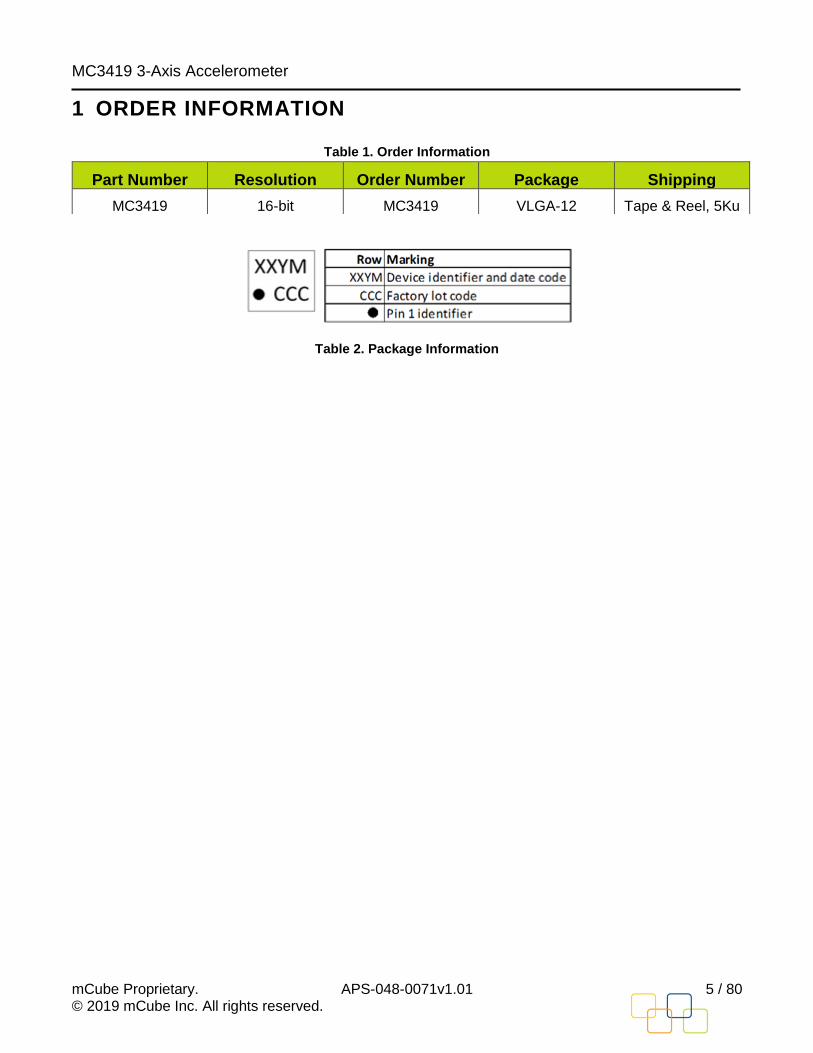
1 ORDER INFORMATION
Table 1. Order Information
Table 2. Package Information
Part Number Resolution Order Number Package Shipping
MC3419 16-bit MC3419 VLGA-12 Tape & Reel, 5Ku
MC3419 3-Axis Accelerometer
mCube Proprietary. APS-048-0071v1.01 6 / 80 © 2019 mCube Inc. All rights reserved.
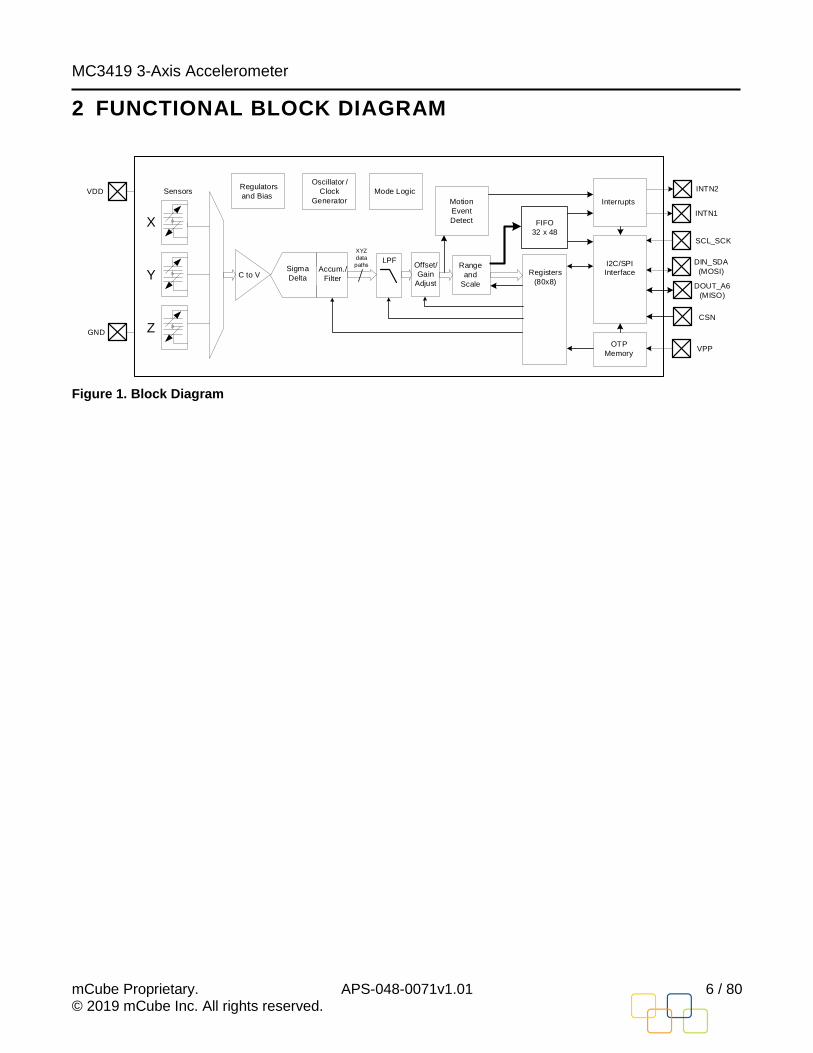
2 FUNCTIONAL BLOCK DIAGRAM
Sigma
DeltaC to V
VPP
VDD
GND
Regulators
and Bias
Oscillator /
Clock
Generator
Mode Logic
I2C/SPIInterface
Interrupts
X
Y
ZOTP
Memory
Registers
(80x8)
SCL_SCK
DIN_SDA
(MOSI)
INTN1
Sensors
Motion
Event
Detect FIFO
32 x 48
Range
and
Scale DOUT_A6
(MISO)
CSN
INTN2
LPFOffset/
Gain
Adjust
Accum./
Filter
XYZ
data
paths
Figure 1. Block Diagram
MC3419 3-Axis Accelerometer
mCube Proprietary. APS-048-0071v1.01 7 / 80 © 2019 mCube Inc. All rights reserved.
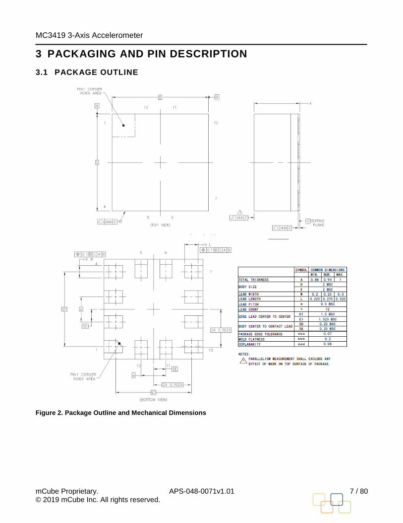
3 PACKAGING AND PIN DESCRIPTION
3.1 PACKAGE OUTLINE
Figure 2. Package Outline and Mechanical Dimensions
MC3419 3-Axis Accelerometer
mCube Proprietary. APS-048-0071v1.01 8 / 80 © 2019 mCube Inc. All rights reserved.
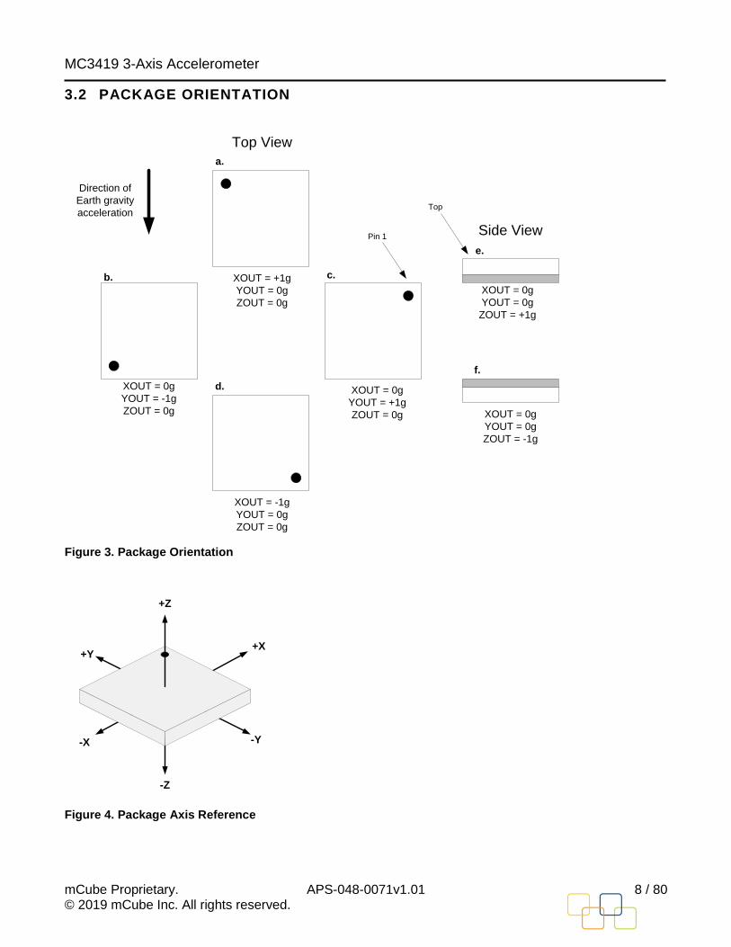
3.2 PACKAGE ORIENTATION
Direction of
Earth gravity
acceleration
XOUT = -1g
YOUT = 0g
ZOUT = 0g
XOUT = +1g
YOUT = 0g
ZOUT = 0g
XOUT = 0g
YOUT = -1g
ZOUT = 0g
XOUT = 0g
YOUT = +1g
ZOUT = 0g
XOUT = 0g
YOUT = 0g
ZOUT = +1g
XOUT = 0g
YOUT = 0g
ZOUT = -1g
Top View
Side ViewPin 1
Top
a.
b. c.
d.
e.
f.
Figure 3. Package Orientation
-X
+X+Y
-Y
+Z
-Z
Figure 4. Package Axis Reference

MC3419 3-Axis Accelerometer
mCube Proprietary. APS-048-0071v1.01 9 / 80 © 2019 mCube Inc. All rights reserved.
3.3 PIN DESCRIPTION
Pin Name Function
1 DOUT_A6 SPI data output
I2C address bit 6
2 DIN_SDA 1 SPI data In
I2C serial data input/output
3 NC No connect
4 VPP Connect to GND
5 INTN 1 2 Interrupt active LOW 3
6 INTN 2 2 Interrupt active LOW 3
7 VDD Power supply for internal
8 NC No Connect
9 GND Ground
10 CSN SPI chip select (active low)
11 NC No connect
12 SCK_SCL 1 I2C/SPI serial clock input
Table 3. Pin Description
Notes:
1) This pin requires a pull-up resistor, typically 4.7kΩ to pin VDD. Refer to I2C Specification for Fast-Mode devices. Higher resistance values can be used (typically done to reduce current leakage) but such applications are outside the scope of this datasheet.
2) This pin can be configured by software to operate either as an open-drain output or push-pull output (see GPIO control register, address 0x33). If set to open-drain, then it requires a pull-up resistor, typically 4.7kΩ to VDD.
3) INTN pin polarity is programmable in the GPIO control register, address 0x33.
MC3419 3-Axis Accelerometer
mCube Proprietary. APS-048-0071v1.01 10 / 80 © 2019 mCube Inc. All rights reserved.
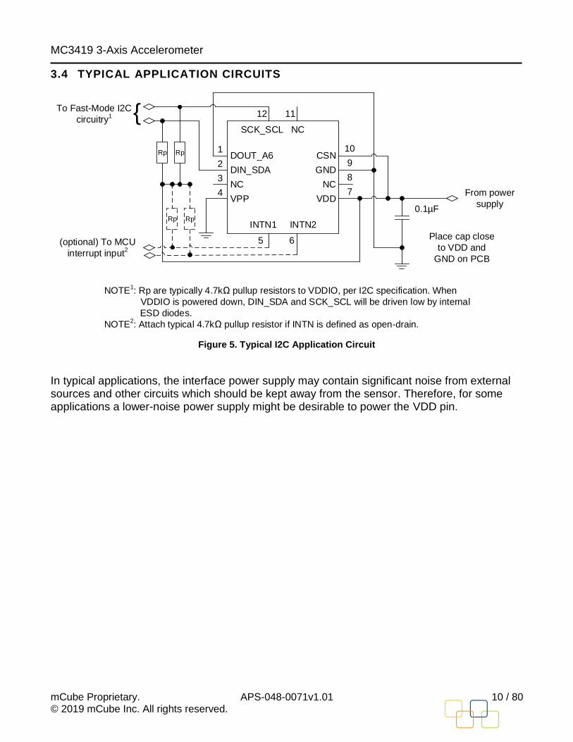
3.4 TYPICAL APPLICATION CIRCUITS
To Fast-Mode I2C
circuitry1
NOTE1: Rp are typically 4.7kΩ pullup resistors to VDDIO, per I2C specification. When
VDDIO is powered down, DIN_SDA and SCK_SCL will be driven low by internal
ESD diodes.
NOTE2: Attach typical 4.7kΩ pullup resistor if INTN is defined as open-drain.
From power
supply
DOUT_A6
DIN_SDA
NC
VPP
CSN
GND
NC
VDD
SCK_SCL NC
INTN1 INTN2
0.1µF
Place cap close
to VDD and
GND on PCB
(optional) To MCU
interrupt input2
1
2
3
4
10
9
8
7
5 6
12 11
Rp Rp
Rp Rp
Figure 5. Typical I2C Application Circuit
In typical applications, the interface power supply may contain significant noise from external sources and other circuits which should be kept away from the sensor. Therefore, for some applications a lower-noise power supply might be desirable to power the VDD pin.
MC3419 3-Axis Accelerometer
mCube Proprietary. APS-048-0071v1.01 11 / 80 © 2019 mCube Inc. All rights reserved.
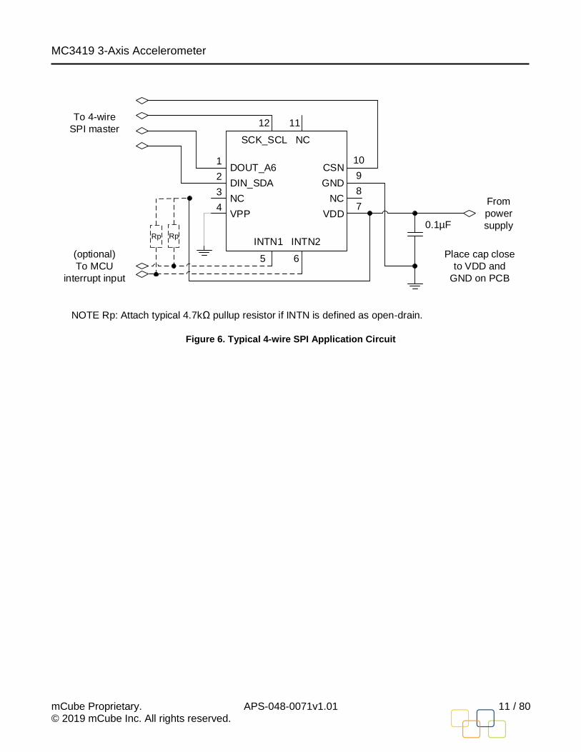
To 4-wire
SPI master
NOTE Rp: Attach typical 4.7kΩ pullup resistor if INTN is defined as open-drain.
From
power
supply
DOUT_A6
DIN_SDA
NC
VPP
CSN
GND
NC
VDD
SCK_SCL NC
INTN1 INTN2
0.1µF
Place cap close
to VDD and
GND on PCB
(optional)
To MCU
interrupt input
1
2
3
4
10
9
8
7
5 6
12 11
RpRp
Figure 6. Typical 4-wire SPI Application Circuit
MC3419 3-Axis Accelerometer
mCube Proprietary. APS-048-0071v1.01 12 / 80 © 2019 mCube Inc. All rights reserved.
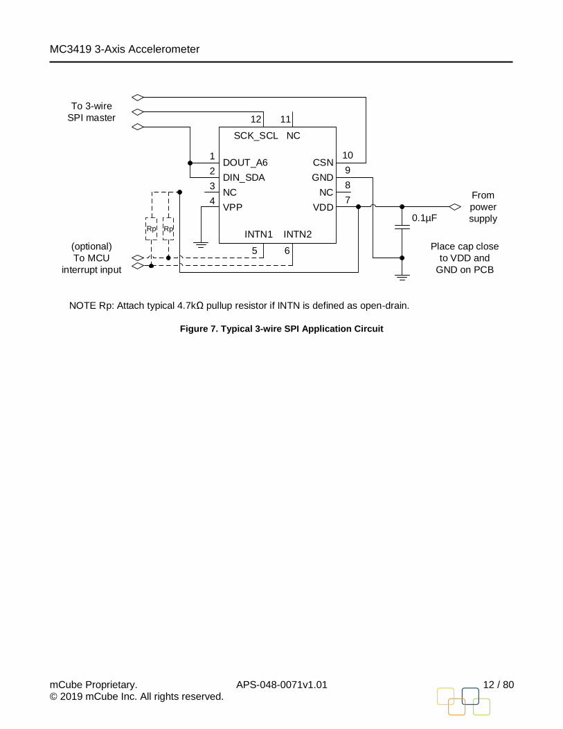
To 3-wire
SPI master
NOTE Rp: Attach typical 4.7kΩ pullup resistor if INTN is defined as open-drain.
From
power
supply
DOUT_A6
DIN_SDA
NC
VPP
CSN
GND
NC
VDD
SCK_SCL NC
INTN1 INTN2
0.1µF
Place cap close
to VDD and
GND on PCB
(optional)
To MCU
interrupt input
1
2
3
4
10
9
8
7
5 6
12 11
RpRp
Figure 7. Typical 3-wire SPI Application Circuit
MC3419 3-Axis Accelerometer
mCube Proprietary. APS-048-0071v1.01 13 / 80 © 2019 mCube Inc. All rights reserved.
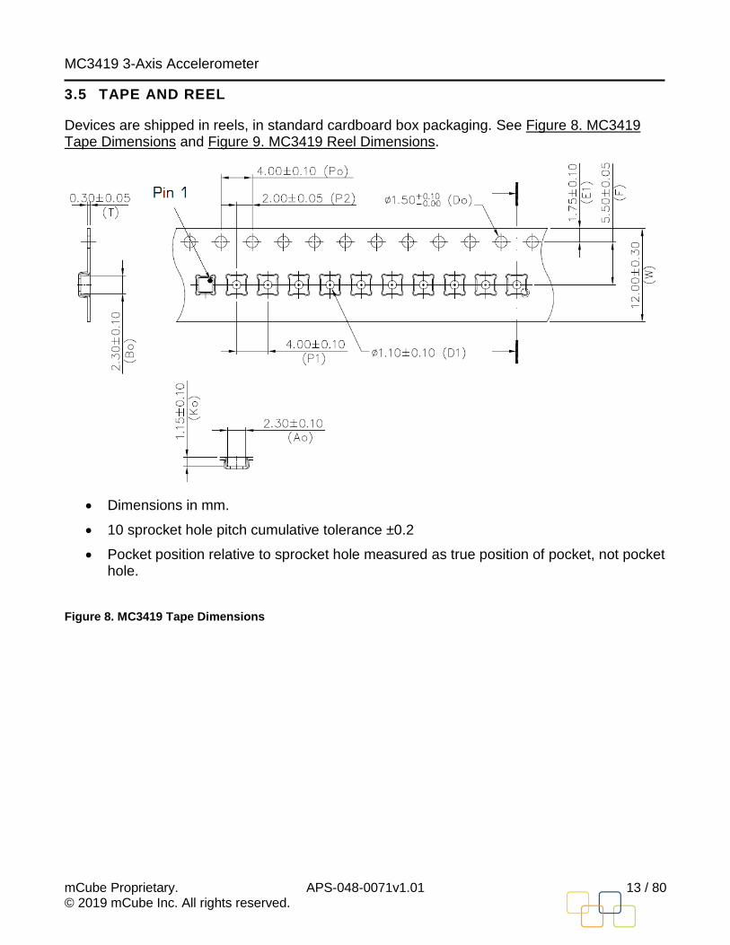
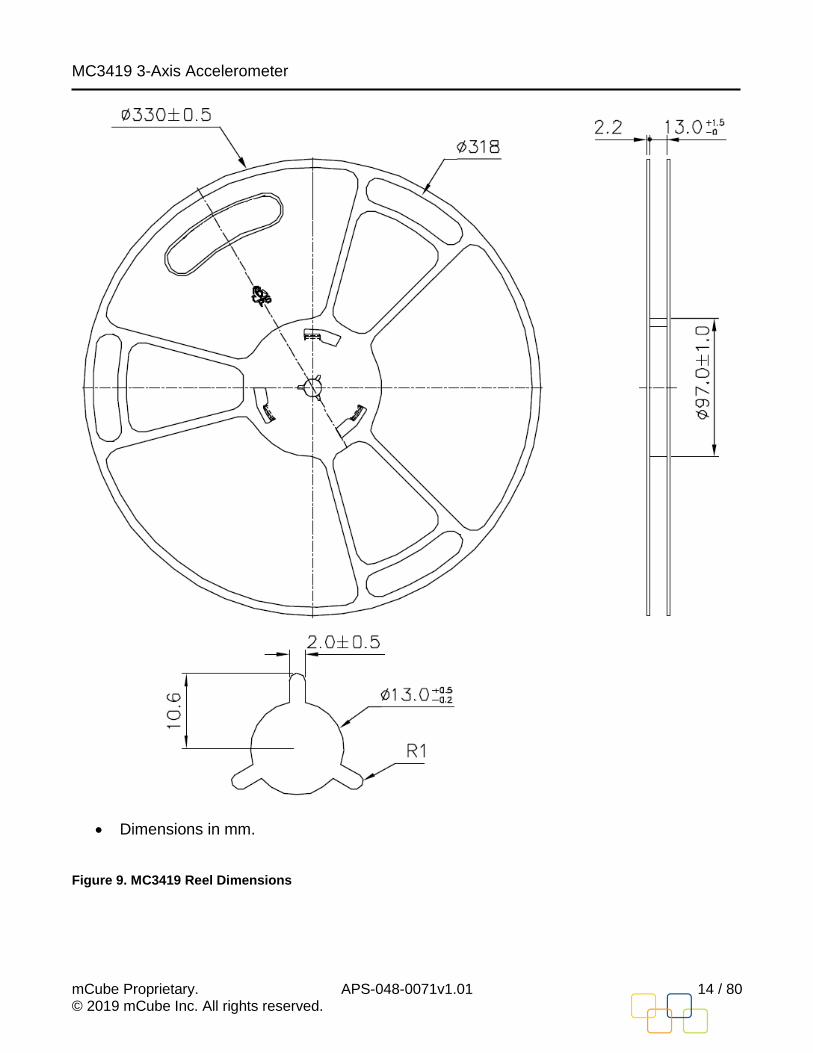
3.5 TAPE AND REEL
Devices are shipped in reels, in standard cardboard box packaging. See Figure 8. MC3419 Tape Dimensions and Figure 9. MC3419 Reel Dimensions.
• Dimensions in mm.
• 10 sprocket hole pitch cumulative tolerance ±0.2
• Pocket position relative to sprocket hole measured as true position of pocket, not pocket hole.
Figure 8. MC3419 Tape Dimensions
MC3419 3-Axis Accelerometer
mCube Proprietary. APS-048-0071v1.01 14 / 80 © 2019 mCube Inc. All rights reserved.
• Dimensions in mm.
Figure 9. MC3419 Reel Dimensions

MC3419 3-Axis Accelerometer
mCube Proprietary. APS-048-0071v1.01 15 / 80 © 2019 mCube Inc. All rights reserved.
3.6 SOLDERING PROFILE
The LGA package follows the reflow soldering classification profiles described in Joint Industry Standard, Moisture/Reflow Sensitivity Classification for Nonhermetic Surface Mount Devices, document number J-STD-020E. Reflow soldering has a peak temperature (Tp) of 260⁰C
3.7 SHIPPING AND HANDLING GUIDELINES
Shipping and handling follow the standards described in Joint Industry Standard, Handling, Packing, Shipping and Use of Moisture/Reflow Sensitive Surface Mount Devices, document number J-STD-033C.
The following are additional handling guidelines (refer to the mCube document, PCB Design, Device Handling and Assembly Guidelines, document number AN-001, for more information):
• While the mechanical sensor is designed to handle high-g shock events, direct mechanical shock to the package should be avoided.
• SMT assembly houses should use automated assembly equipment with either plastic nozzles or nozzles with compliant tips (for example, soft rubber or silicone).
• Avoid g-forces beyond the specified limits during transportation.
• Handling and mounting of sensors should be done in a defined and qualified installation.
3.8 MOISTURE SENSITIVITY LEVEL CONTROL
The following are storage recommendations (refer to the mCube document, PCB Design, Device Handling and Assembly Guidelines, document number AN-001, for more information):
• Store the tape and reel in the unopened dry pack, until required on the assembly floor.
• If the dry pack has been opened or the reel has been removed from the dry pack, reseal the reel inside of the dry pack with a black protective belt. Avoid crushing the tape and reel.
• Store the cardboard box in a vertical position.
MC3419 3-Axis Accelerometer
mCube Proprietary. APS-048-0071v1.01 16 / 80 © 2019 mCube Inc. All rights reserved.
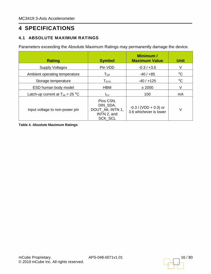
4 SPECIFICATIONS
4.1 ABSOLUTE MAXIMUM RATINGS
Parameters exceeding the Absolute Maximum Ratings may permanently damage the device.
Rating Symbol Minimum /
Maximum Value Unit
Supply Voltages Pin VDD -0.3 / +3.6 V
Ambient operating temperature TOP -40 / +85 ⁰C
Storage temperature TSTG -40 / +125 ⁰C
ESD human body model HBM ± 2000 V
Latch-up current at Top = 25 ⁰C ILU 100 mA
Input voltage to non-power pin
Pins CSN, DIN_SDA,
DOUT_A6, INTN 1, INTN 2, and SCK_SCL
-0.3 / (VDD + 0.3) or 3.6 whichever is lower
V
Table 4. Absolute Maximum Ratings
MC3419 3-Axis Accelerometer
mCube Proprietary. APS-048-0071v1.01 17 / 80 © 2019 mCube Inc. All rights reserved.
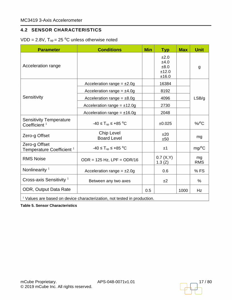
4.2 SENSOR CHARACTERISTICS
VDD = 2.8V, Top = 25 ⁰C unless otherwise noted
Parameter Conditions Min Typ Max Unit
Acceleration range
±2.0 ±4.0 ±8.0 ±12.0 ±16.0
g
Sensitivity
Acceleration range = ±2.0g 16384
LSB/g
Acceleration range = ±4.0g 8192
Acceleration range = ±8.0g 4096
Acceleration range = ±12.0g 2730
Acceleration range = ±16.0g 2048
Sensitivity Temperature Coefficient 1 -40 ≤ Top ≤ +85 ⁰C
±0.025 %/⁰C
Zero-g Offset Chip Level
Board Level ±20 ±50
mg
Zero-g Offset Temperature Coefficient 1 -40 ≤ Top ≤ +85 ⁰C ±1 mg/⁰C
RMS Noise ODR = 125 Hz, LPF = ODR/16 0.7 (X,Y) 1.3 (Z)
mg
RMS
Nonlinearity 1 Acceleration range = ±2.0g 0.6 % FS
Cross-axis Sensitivity 1 Between any two axes ±2 %
ODR, Output Data Rate 0.5 1000 Hz
1 Values are based on device characterization, not tested in production.
Table 5. Sensor Characteristics
MC3419 3-Axis Accelerometer
mCube Proprietary. APS-048-0071v1.01 18 / 80 © 2019 mCube Inc. All rights reserved.
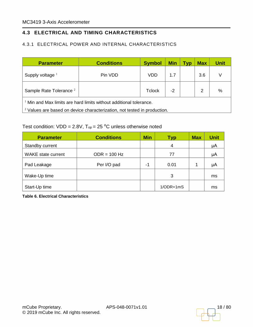
4.3 ELECTRICAL AND TIMING CHARACTERISTICS
4.3.1 ELECTRICAL POWER AND INTERNAL CHARACTERISTICS
Parameter Conditions Symbol Min Typ Max Unit
Supply voltage 1 Pin VDD VDD 1.7
3.6 V
Sample Rate Tolerance 2
Tclock -2 2 %
1 Min and Max limits are hard limits without additional tolerance.
2 Values are based on device characterization, not tested in production.
Test condition: VDD = 2.8V, Top = 25 ⁰C unless otherwise noted
Parameter Conditions Min Typ Max Unit
Standby current 4
μA
WAKE state current ODR = 100 Hz 77
μA
Pad Leakage Per I/O pad -1 0.01 1 μA
Wake-Up time 3 ms
Start-Up time 1/ODR+1mS ms
Table 6. Electrical Characteristics
MC3419 3-Axis Accelerometer
mCube Proprietary. APS-048-0071v1.01 19 / 80 © 2019 mCube Inc. All rights reserved.
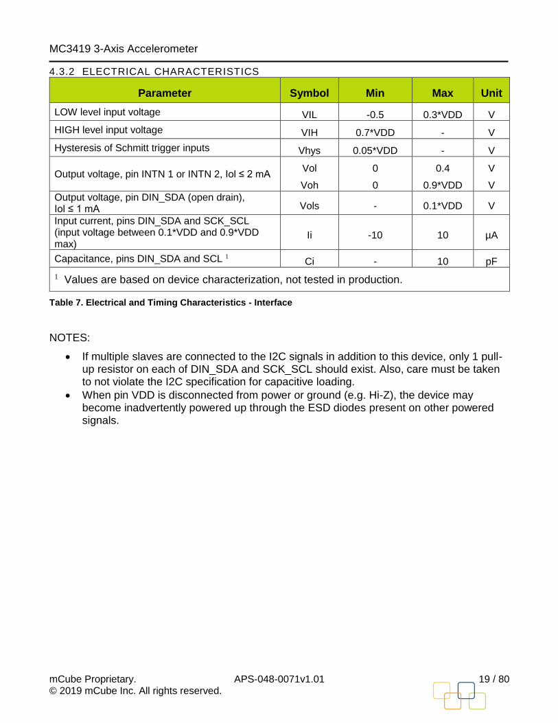
4.3.2 ELECTRICAL CHARACTERISTICS
Parameter Symbol Min Max Unit
LOW level input voltage VIL -0.5 0.3*VDD V
HIGH level input voltage VIH 0.7*VDD - V
Hysteresis of Schmitt trigger inputs Vhys 0.05*VDD - V
Output voltage, pin INTN 1 or INTN 2, Iol ≤ 2 mA Vol
Voh
0
0
0.4
0.9*VDD
V
V
Output voltage, pin DIN_SDA (open drain), Iol ≤ 1 mA Vols - 0.1*VDD V
Input current, pins DIN_SDA and SCK_SCL (input voltage between 0.1*VDD and 0.9*VDD max)
Ii -10 10 µA
Capacitance, pins DIN_SDA and SCL 1 Ci - 10 pF
1 Values are based on device characterization, not tested in production.
Table 7. Electrical and Timing Characteristics - Interface
NOTES:
• If multiple slaves are connected to the I2C signals in addition to this device, only 1 pull-up resistor on each of DIN_SDA and SCK_SCL should exist. Also, care must be taken to not violate the I2C specification for capacitive loading.
• When pin VDD is disconnected from power or ground (e.g. Hi-Z), the device may become inadvertently powered up through the ESD diodes present on other powered signals.
MC3419 3-Axis Accelerometer
mCube Proprietary. APS-048-0071v1.01 20 / 80 © 2019 mCube Inc. All rights reserved.
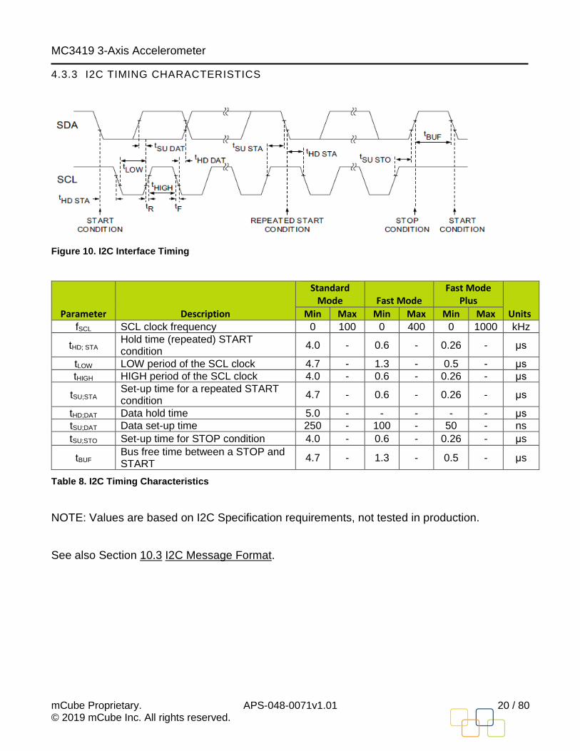
4.3.3 I2C TIMING CHARACTERISTICS
Figure 10. I2C Interface Timing
Parameter Description
Standard Mode Fast Mode
Fast Mode Plus
Units Min Max Min Max Min Max
fSCL SCL clock frequency 0 100 0 400 0 1000 kHz
tHD; STA Hold time (repeated) START condition
4.0 - 0.6 - 0.26 - μs
tLOW LOW period of the SCL clock 4.7 - 1.3 - 0.5 - μs
tHIGH HIGH period of the SCL clock 4.0 - 0.6 - 0.26 - μs
tSU;STA Set-up time for a repeated START condition
4.7 - 0.6 - 0.26 - μs
tHD;DAT Data hold time 5.0 - - - - - μs
tSU;DAT Data set-up time 250 - 100 - 50 - ns
tSU;STO Set-up time for STOP condition 4.0 - 0.6 - 0.26 - μs
tBUF Bus free time between a STOP and START
4.7 - 1.3 - 0.5 - μs
Table 8. I2C Timing Characteristics
NOTE: Values are based on I2C Specification requirements, not tested in production.
See also Section 10.3 I2C Message Format.
MC3419 3-Axis Accelerometer
mCube Proprietary. APS-048-0071v1.01 21 / 80 © 2019 mCube Inc. All rights reserved.
5 GENERAL OPERATION
The device supports the reading of samples and device status upon interrupt or by polling.
5.1 SENSOR SAMPLING
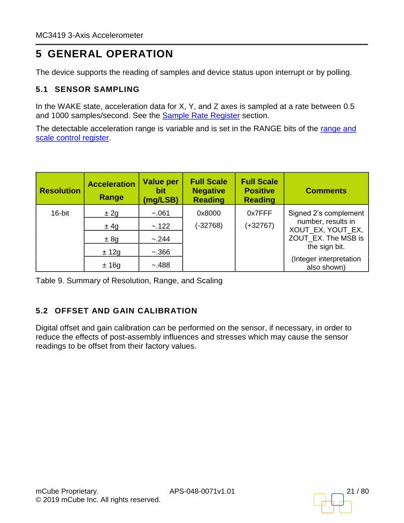
In the WAKE state, acceleration data for X, Y, and Z axes is sampled at a rate between 0.5 and 1000 samples/second. See the Sample Rate Register section.
The detectable acceleration range is variable and is set in the RANGE bits of the range and scale control register.
Resolution Acceleration
Range
Value per bit
(mg/LSB)
Full Scale Negative Reading
Full Scale Positive Reading
Comments
16-bit
± 2g ~.061 0x8000
(-32768)
0x7FFF
(+32767)
Signed 2’s complement number, results in
XOUT_EX, YOUT_EX, ZOUT_EX. The MSB is
the sign bit.
(Integer interpretation also shown)
± 4g ~.122
± 8g ~.244
± 12g ~.366
± 16g ~.488
Table 9. Summary of Resolution, Range, and Scaling
5.2 OFFSET AND GAIN CALIBRATION
Digital offset and gain calibration can be performed on the sensor, if necessary, in order to reduce the effects of post-assembly influences and stresses which may cause the sensor readings to be offset from their factory values.
MC3419 3-Axis Accelerometer
mCube Proprietary. APS-048-0071v1.01 22 / 80 © 2019 mCube Inc. All rights reserved.
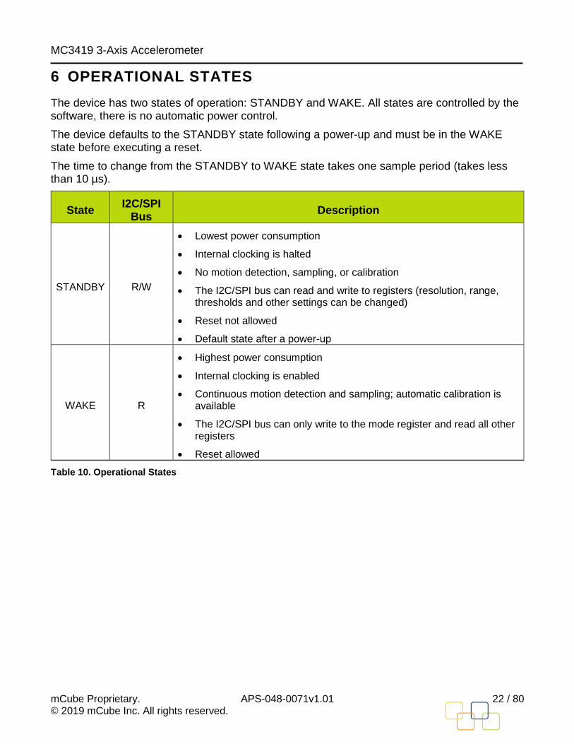
6 OPERATIONAL STATES
The device has two states of operation: STANDBY and WAKE. All states are controlled by the software, there is no automatic power control.
The device defaults to the STANDBY state following a power-up and must be in the WAKE state before executing a reset.
The time to change from the STANDBY to WAKE state takes one sample period (takes less than 10 µs).
State I2C/SPI
Bus Description
STANDBY R/W
• Lowest power consumption
• Internal clocking is halted
• No motion detection, sampling, or calibration
• The I2C/SPI bus can read and write to registers (resolution, range, thresholds and other settings can be changed)
• Reset not allowed
• Default state after a power-up
WAKE R
• Highest power consumption
• Internal clocking is enabled
• Continuous motion detection and sampling; automatic calibration is available
• The I2C/SPI bus can only write to the mode register and read all other registers
• Reset allowed
Table 10. Operational States
MC3419 3-Axis Accelerometer
mCube Proprietary. APS-048-0071v1.01 23 / 80 © 2019 mCube Inc. All rights reserved.
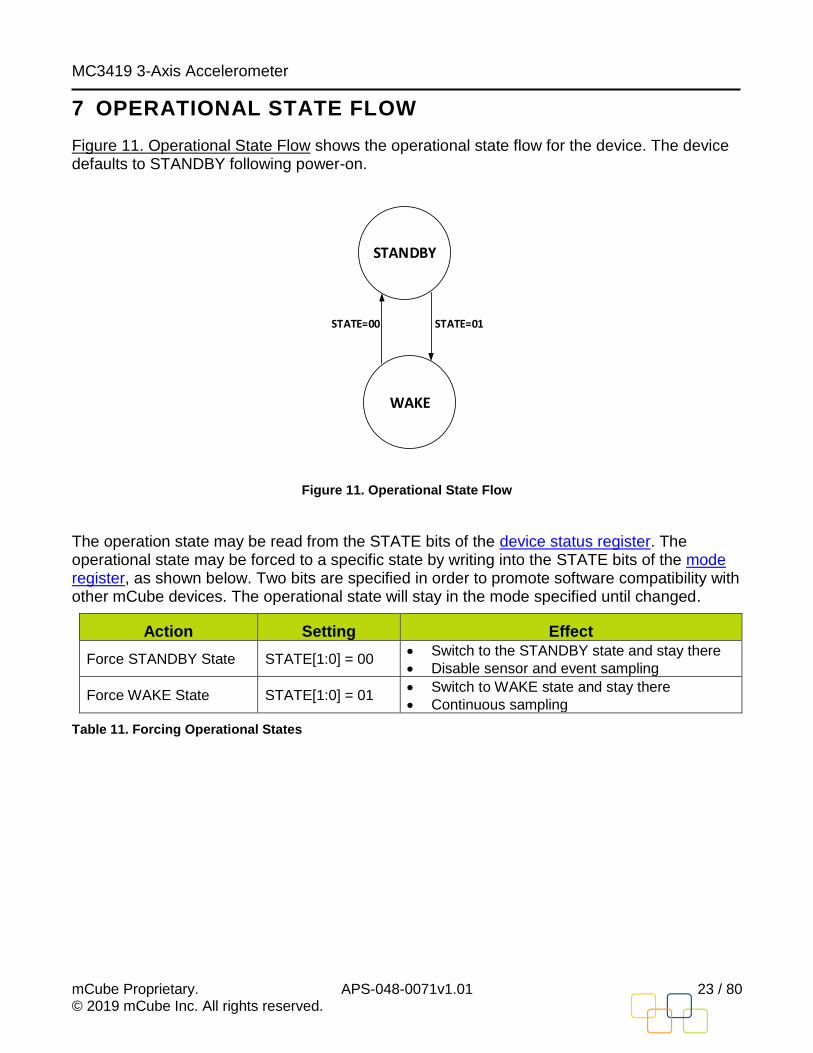
7 OPERATIONAL STATE FLOW
Figure 11. Operational State Flow shows the operational state flow for the device. The device defaults to STANDBY following power-on.
WAKE
STANDBY
STATE=00 STATE=01
Figure 11. Operational State Flow
The operation state may be read from the STATE bits of the device status register. The operational state may be forced to a specific state by writing into the STATE bits of the mode register, as shown below. Two bits are specified in order to promote software compatibility with other mCube devices. The operational state will stay in the mode specified until changed.
Action Setting Effect
Force STANDBY State STATE[1:0] = 00 • Switch to the STANDBY state and stay there
• Disable sensor and event sampling
Force WAKE State STATE[1:0] = 01 • Switch to WAKE state and stay there
• Continuous sampling
Table 11. Forcing Operational States
MC3419 3-Axis Accelerometer
mCube Proprietary. APS-048-0071v1.01 24 / 80 © 2019 mCube Inc. All rights reserved.
8 INTERRUPTS
The sensor device utilizes output pin INTN 1 or INTN 2 to signal to an external microprocessor that an event has been detected. The microprocessor should contain an interrupt service routine which would perform certain tasks after receiving this interrupt and reading the associated status bits, perhaps after a sample was made ready. If interrupts are to be used, the microprocessor must set up the registers in the sensor so that when a specific event is detected, the microprocessor would receive the interrupt and the interrupt service routine would be executed. If polling is used, there is no need for the interrupt registers to be set up.
For products that use polling, the microprocessor must periodically poll the sensor and read the status data (the INTN 1 or INTN 2 pin is not used). For most applications, this is likely best done at the sensor sampling rate or faster.
NOTE: At least one I2C STOP condition must be present between samples for the sensor to update the sample data registers.
8.1 INTERRUPT OVERVIEW
Feature Description Comment
Interrupt Pins Two interrupt Pins are supported: INTN1 INTN2
Interrupt Polarity INTN1 and INTN2 pins operate in open-drain and active-drive modes. The polarity of the interrupts is independently selectable.
The interrupt polarity/drive mode bits are in the GPIO control register 0x33.
Interrupt Sources 1 interrupt on sample 5 motion interrupts 3 FIFO interrupts
The default setting is to route SAMPLE+MOTION interrupt requests (INT1_REQ) to INTN1 pin and FIFO interrupt requests (INT2_REQ) to the INTN2 pin.
Interrupt Servicing Interrupts may be cleared globally or individually. All interrupts are cleared by writing to register 0x14. FIFO interrupt bits are loaded in register 0x2F.
Global clearing is the default, use register 0x31 bit 6 (INDIV_INTR_CLR) to enable the individual interrupt clear option (bitmask mode). Read/writing to register 0x2F does not clear FIFO interrupts.
Swapping or Combining Interrupt Requests
INT1_REQ (sample + motion) and INT2_REQ (FIFO) may be swapped between the INTN1 and INTN2 pins, or combined on a single INTN1 pin.
If all interrupts are combined in a single source, the pin to be used can still be chosen by using register 0x31 bit 4.
Table 12. Interrupt Overview

MC3419 3-Axis Accelerometer
mCube Proprietary. APS-048-0071v1.01 25 / 80 © 2019 mCube Inc. All rights reserved.
8.2 ENABLING AND CLEARING INTERRUPTS
The interrupt status register (0x14) contains the bits for the sample acquisition interrupt ACQ_INT and the motion interrupts. The FIFO interrupt status register (0x2F) contains the bits for the FIFO interrupts The interrupt enable register (0x06) and FIFO control register (0x2D) determine if a flag event generates interrupts.
The interrupts are cleared and rearmed every time the interrupt status register (0x14) is written. Interrupts may be cleared globally or individually.
When an event is detected, it is masked with a flag bit in the interrupt enable register, and then the corresponding status bit is set in the status registers.
The polarity and driving mode of the external interrupt signals may be chosen by setting the INTN1 or INTN2 IPP and IAH bits in the GPIO control register (0x33).
8.3 INTERRUPT SOURCES
8.3.1 ACQ_INT INTERRUPT
The ACQ_INT flag bit in the status registers is always active. This bit is cleared when it is read. When a sample has been produced, an interrupt will be generated only if the ACQ_INT_EN bit in the interrupt enable register is active. The frequency of the ACQ_INT bit being set active is always the same as the sample rate.
8.3.2 TILT/FLIP (TILT_INT, FLIP_INT)
The TILT and FLIP flag bits in register 0x03/0x13 bit are active when the TILT/FLIP features are enabled by register 0x9 bit 0. The flag bits can transition quickly, so polled operation may be difficult. It is recommended to use the interrupt register 0x04/0x14 bits 0 or 1 instead. Note that the TILT and FLIP interrupt enables in register 0x06 bits [1:0] are separate, although there is a single control bit in register 0x09.
8.3.3 INTERRUPT ON ANYMOTION (ANYM_INT)
The ANYM flag bit in register 0x03/0x13 bit is active when the ANYM feature is enabled by register 0x9 bit 2. The flag bit can transition quickly, so polled operation may be difficult. It is recommended to use the interrupt in register 0x04/0x14 bit 2 instead. Note that the SHAKE and TILT_35 interrupts require the ANYM feature to be enabled in register 0x09 bit 2, but the ANYM interrupt enable in register 0x06 bit 2 is not required.
8.3.4 INTERRUPT ON SHAKE (SHAKE_INT)
The SHAKE flag bit in register 0x03/0x13 bit is active when the SHAKE feature is enabled by register 0x9 bit 3. The flag bit can transition quickly, so polled operation may be difficult. It is recommended to use the interrupt register 0x04/0x14 bit 3 instead. Note that the SHAKE interrupt requires the ANYM feature to be enabled in register 0x09 bit 2, but the ANYM interrupt enable in register 0x06 bit 2 is not required.
MC3419 3-Axis Accelerometer
mCube Proprietary. APS-048-0071v1.01 26 / 80 © 2019 mCube Inc. All rights reserved.
8.3.5 INTERRUPT ON TILT_35 (TILT_35_INT)
The TILT_35 flag bit in register 0x03/0x13 bit is active when the SHAKE feature is enabled by register 0x9 bit 4. The flag bit can transition quickly, so polled operation may be difficult. It is recommended to use the interrupt register 0x04/0x14 bit 4 instead. Note that the TILT_35 interrupt requires the ANYM feature to be enabled in register 0x09 bit 2, but the ANYM interrupt enable in register 0x06 bit 2 is not required.
8.3.6 INTERRUPT ON FIFO EMPTY (FIFO_EMPTY_INT)
The FIFO_EMPTY flag bit in register 0x0A bit 0 is active when the FIFO enable (FIFO_EN) control is enabled in register 0x2D bit 5. The FIFO_EMPTY flag will be set to ‘1’ following a POR or SW_RESET because the default state of the FIFO is empty. Note that the FIFO_EMPTY bit may transition on any write or read to the FIFO. The FIFO_EMPTY_INT_EN interrupt control bit is at register 0x2D bit 0. No bits in register 0x06 are required to be set.
8.3.7 INTERRUPT ON FIFO FULL (FIFO_FULL_INT)
The FIFO_FULL flag bit in register 0x0A bit 1 is active when the FIFO enable (FIFO_EN) control is enabled in register 0x2D bit 5. The FIFO_FULL flag will be set to ‘0’ following a POR or SW_RESET because the default state of the FIFO is empty. Note that the FIFO_FULL bit may transition on any write or read to the FIFO. The FIFO_FULL_INT_EN interrupt control bit is at register 0x2D bit 1. No bits in register 0x06 are required to be set.
8.3.8 INTERRUPT ON FIFO THRESHOLD (FIFO_THRESH_INT)
The FIFO_THRESH flag bit in register 0x0A bit 2 is active when the FIFO enable (FIFO_EN) control is enabled in register 0x2D bit 5. The FIFO_THRESH flag will be set to ‘0’ following a POR or SW_RESET because the default state of the FIFO is empty, and the default threshold level is a count of 16 samples (located in register 0x2E). Note that the FIFO_THRESH bit may transition on any write or read to the FIFO when a threshold level is crossed. The FIFO_THERESH_INT_EN interrupt control bit is at register 0x2D bit 2. No bits in register 0x06 are required to be set.
MC3419 3-Axis Accelerometer
mCube Proprietary. APS-048-0071v1.01 27 / 80 © 2019 mCube Inc. All rights reserved.
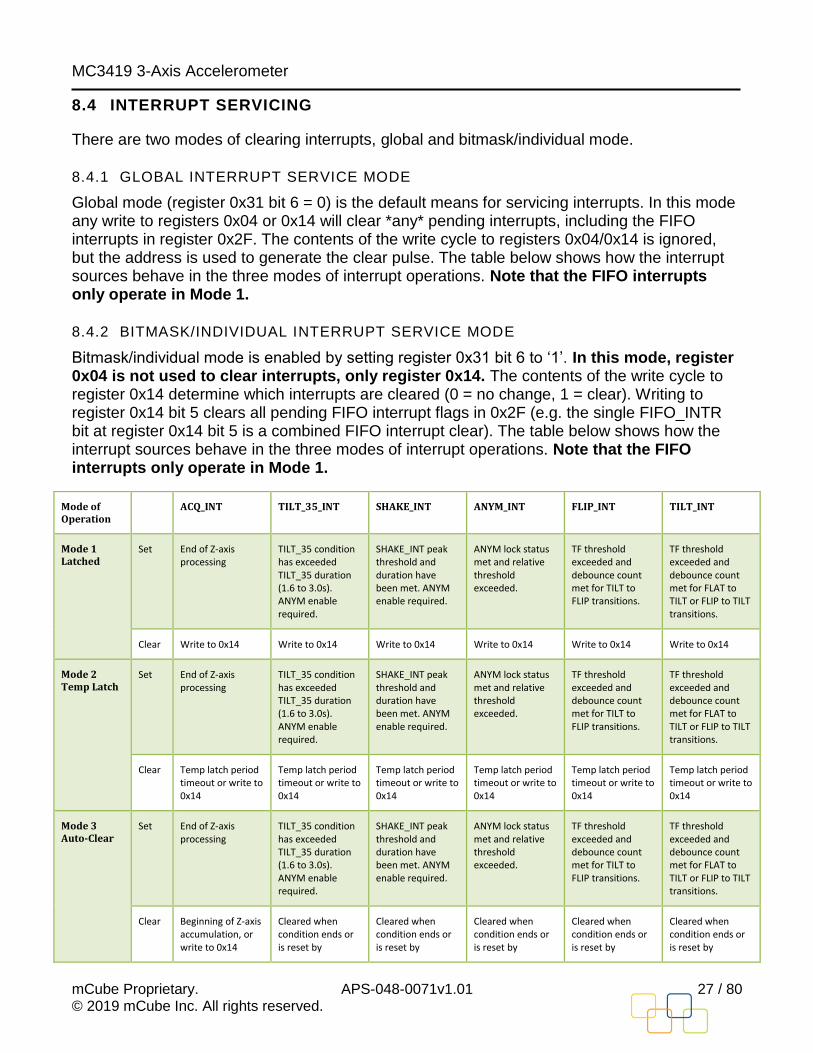
8.4 INTERRUPT SERVICING
There are two modes of clearing interrupts, global and bitmask/individual mode.
8.4.1 GLOBAL INTERRUPT SERVICE MODE
Global mode (register 0x31 bit 6 = 0) is the default means for servicing interrupts. In this mode any write to registers 0x04 or 0x14 will clear *any* pending interrupts, including the FIFO interrupts in register 0x2F. The contents of the write cycle to registers 0x04/0x14 is ignored, but the address is used to generate the clear pulse. The table below shows how the interrupt sources behave in the three modes of interrupt operations. Note that the FIFO interrupts only operate in Mode 1.
8.4.2 BITMASK/INDIVIDUAL INTERRUPT SERVICE MODE
Bitmask/individual mode is enabled by setting register 0x31 bit 6 to ‘1’. In this mode, register 0x04 is not used to clear interrupts, only register 0x14. The contents of the write cycle to register 0x14 determine which interrupts are cleared (0 = no change, 1 = clear). Writing to register 0x14 bit 5 clears all pending FIFO interrupt flags in 0x2F (e.g. the single FIFO_INTR bit at register 0x14 bit 5 is a combined FIFO interrupt clear). The table below shows how the interrupt sources behave in the three modes of interrupt operations. Note that the FIFO interrupts only operate in Mode 1.
Mode of Operation
ACQ_INT TILT_35_INT SHAKE_INT ANYM_INT FLIP_INT TILT_INT
Mode 1 Latched
Set End of Z-axis processing
TILT_35 condition has exceeded TILT_35 duration (1.6 to 3.0s). ANYM enable required.
SHAKE_INT peak threshold and duration have been met. ANYM enable required.
ANYM lock status met and relative threshold exceeded.
TF threshold exceeded and debounce count met for TILT to FLIP transitions.
TF threshold exceeded and debounce count met for FLAT to TILT or FLIP to TILT transitions.
Clear Write to 0x14 Write to 0x14 Write to 0x14 Write to 0x14 Write to 0x14 Write to 0x14
Mode 2 Temp Latch
Set End of Z-axis processing
TILT_35 condition has exceeded TILT_35 duration (1.6 to 3.0s). ANYM enable required.
SHAKE_INT peak threshold and duration have been met. ANYM enable required.
ANYM lock status met and relative threshold exceeded.
TF threshold exceeded and debounce count met for TILT to FLIP transitions.
TF threshold exceeded and debounce count met for FLAT to TILT or FLIP to TILT transitions.
Clear Temp latch period timeout or write to 0x14
Temp latch period timeout or write to 0x14
Temp latch period timeout or write to 0x14
Temp latch period timeout or write to 0x14
Temp latch period timeout or write to 0x14
Temp latch period timeout or write to 0x14
Mode 3 Auto-Clear
Set End of Z-axis processing
TILT_35 condition has exceeded TILT_35 duration (1.6 to 3.0s). ANYM enable required.
SHAKE_INT peak threshold and duration have been met. ANYM enable required.
ANYM lock status met and relative threshold exceeded.
TF threshold exceeded and debounce count met for TILT to FLIP transitions.
TF threshold exceeded and debounce count met for FLAT to TILT or FLIP to TILT transitions.
Clear Beginning of Z-axis accumulation, or write to 0x14
Cleared when condition ends or is reset by
Cleared when condition ends or is reset by
Cleared when condition ends or is reset by
Cleared when condition ends or is reset by
Cleared when condition ends or is reset by
MC3419 3-Axis Accelerometer
mCube Proprietary. APS-048-0071v1.01 28 / 80 © 2019 mCube Inc. All rights reserved.
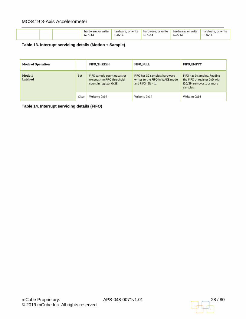
Table 13. Interrupt servicing details (Motion + Sample)
Table 14. Interrupt servicing details (FIFO)
hardware, or write to 0x14
hardware, or write to 0x14
hardware, or write to 0x14
hardware, or write to 0x14
hardware, or write to 0x14
Mode of Operation FIFO_THRESH FIFO_FULL FIFO_EMPTY
Mode 1 Latched
Set FIFO sample count equals or exceeds the FIFO threshold count in register 0x2E.
FIFO has 32 samples; hardware writes to the FIFO in WAKE mode and FIFO_EN = 1.
FIFO has 0 samples. Reading the FIFO at register 0xD with I2C/SPI removes 1 or more samples.
Clear Write to 0x14 Write to 0x14 Write to 0x14
MC3419 3-Axis Accelerometer
mCube Proprietary. APS-048-0071v1.01 29 / 80 © 2019 mCube Inc. All rights reserved.
8.5 INTERRUPT REQUESTS AND EXTERNAL INT PINS
MC3419 has two pins which support external interrupts. Each pin may be separately configured as open-drain or active drive and the polarity is programmable. Note that the drive and polarity control has been moved from register 0x07 to register 0x33.
By default the sample + motion interrupt request is routed to the INTN1 pin, and FIFO interrupt request is routed to the INTN2 pin. These requests may be swapped between the INTN1 pin and INTN2 pin or combined on a single pin.
8.5.1 SELECTING DRIVE AND POLARITY
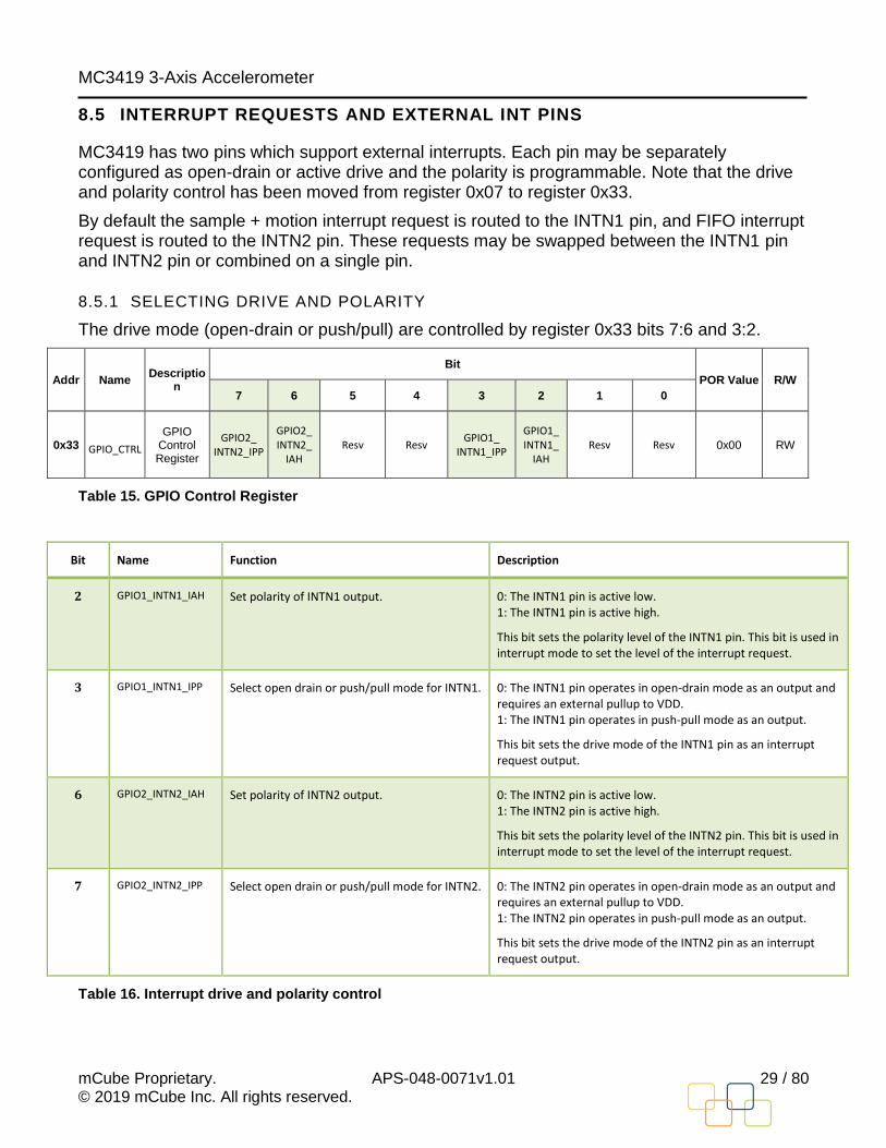
The drive mode (open-drain or push/pull) are controlled by register 0x33 bits 7:6 and 3:2.
Addr Name Descriptio
n
Bit
POR Value R/W
7 6 5 4 3 2 1 0
0x33 GPIO_CTRL
GPIO Control Register
GPIO2_ INTN2_IPP
GPIO2_ INTN2_
IAH Resv Resv
GPIO1_ INTN1_IPP
GPIO1_ INTN1_
IAH Resv Resv 0x00 RW
Table 15. GPIO Control Register
Bit Name Function Description
2 GPIO1_INTN1_IAH Set polarity of INTN1 output. 0: The INTN1 pin is active low. 1: The INTN1 pin is active high.
This bit sets the polarity level of the INTN1 pin. This bit is used in interrupt mode to set the level of the interrupt request.
3 GPIO1_INTN1_IPP Select open drain or push/pull mode for INTN1. 0: The INTN1 pin operates in open-drain mode as an output and requires an external pullup to VDD. 1: The INTN1 pin operates in push-pull mode as an output.
This bit sets the drive mode of the INTN1 pin as an interrupt request output.
6 GPIO2_INTN2_IAH Set polarity of INTN2 output. 0: The INTN2 pin is active low. 1: The INTN2 pin is active high.
This bit sets the polarity level of the INTN2 pin. This bit is used in interrupt mode to set the level of the interrupt request.
7 GPIO2_INTN2_IPP Select open drain or push/pull mode for INTN2. 0: The INTN2 pin operates in open-drain mode as an output and requires an external pullup to VDD. 1: The INTN2 pin operates in push-pull mode as an output.
This bit sets the drive mode of the INTN2 pin as an interrupt request output.
Table 16. Interrupt drive and polarity control
MC3419 3-Axis Accelerometer
mCube Proprietary. APS-048-0071v1.01 30 / 80 © 2019 mCube Inc. All rights reserved.
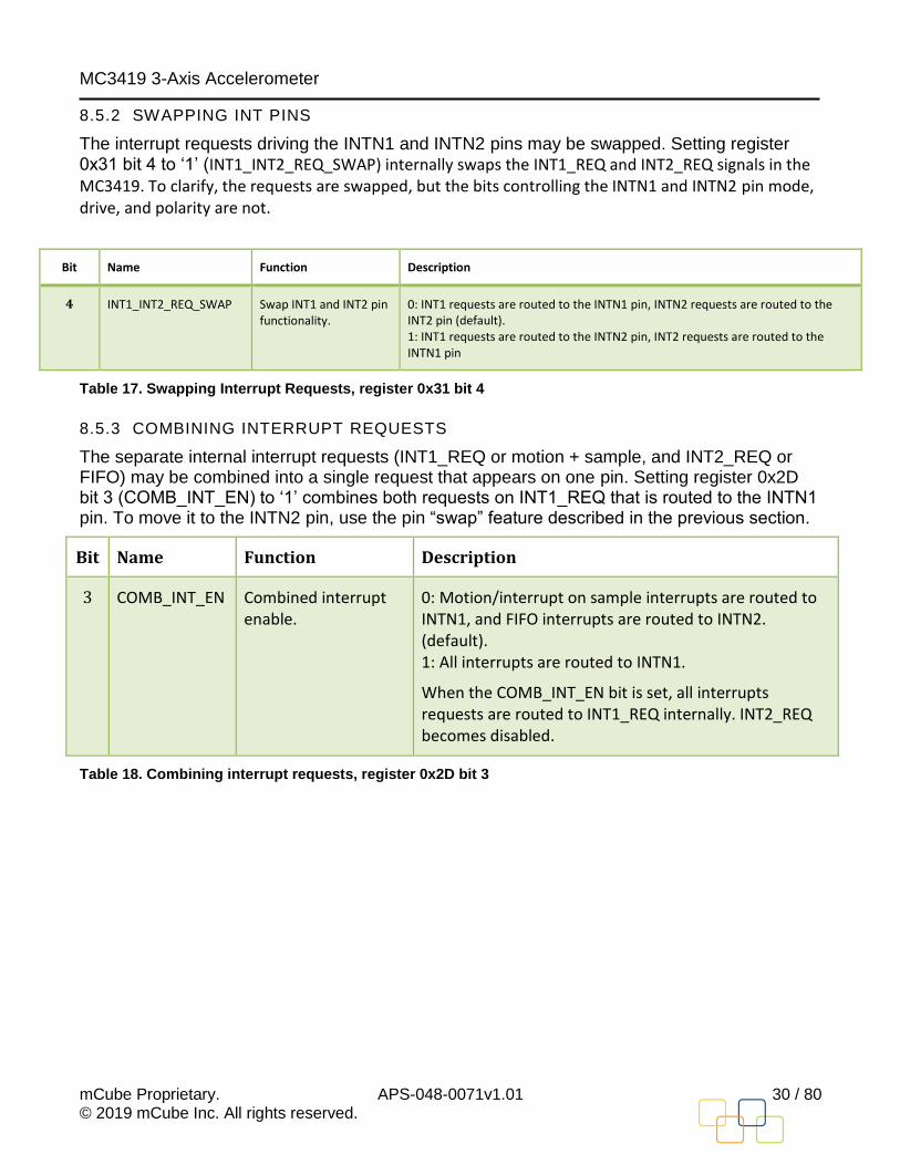
8.5.2 SWAPPING INT PINS
The interrupt requests driving the INTN1 and INTN2 pins may be swapped. Setting register 0x31 bit 4 to ‘1’ (INT1_INT2_REQ_SWAP) internally swaps the INT1_REQ and INT2_REQ signals in the MC3419. To clarify, the requests are swapped, but the bits controlling the INTN1 and INTN2 pin mode, drive, and polarity are not.
Bit Name Function Description
4 INT1_INT2_REQ_SWAP Swap INT1 and INT2 pin functionality.
0: INT1 requests are routed to the INTN1 pin, INTN2 requests are routed to the INT2 pin (default). 1: INT1 requests are routed to the INTN2 pin, INT2 requests are routed to the INTN1 pin
Table 17. Swapping Interrupt Requests, register 0x31 bit 4
8.5.3 COMBINING INTERRUPT REQUESTS
The separate internal interrupt requests (INT1_REQ or motion + sample, and INT2_REQ or FIFO) may be combined into a single request that appears on one pin. Setting register 0x2D bit 3 (COMB_INT_EN) to ‘1’ combines both requests on INT1_REQ that is routed to the INTN1 pin. To move it to the INTN2 pin, use the pin “swap” feature described in the previous section.
Bit Name Function Description
3 COMB_INT_EN Combined interrupt enable.
0: Motion/interrupt on sample interrupts are routed to INTN1, and FIFO interrupts are routed to INTN2. (default). 1: All interrupts are routed to INTN1.
When the COMB_INT_EN bit is set, all interrupts requests are routed to INT1_REQ internally. INT2_REQ becomes disabled.
Table 18. Combining interrupt requests, register 0x2D bit 3
MC3419 3-Axis Accelerometer
mCube Proprietary. APS-048-0071v1.01 31 / 80 © 2019 mCube Inc. All rights reserved.
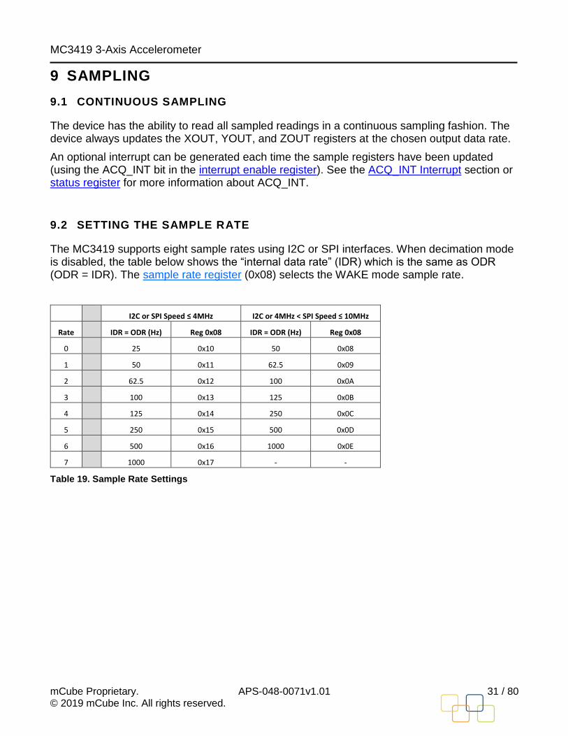
9 SAMPLING
9.1 CONTINUOUS SAMPLING
The device has the ability to read all sampled readings in a continuous sampling fashion. The device always updates the XOUT, YOUT, and ZOUT registers at the chosen output data rate.
An optional interrupt can be generated each time the sample registers have been updated (using the ACQ_INT bit in the interrupt enable register). See the ACQ_INT Interrupt section or status register for more information about ACQ_INT.
9.2 SETTING THE SAMPLE RATE
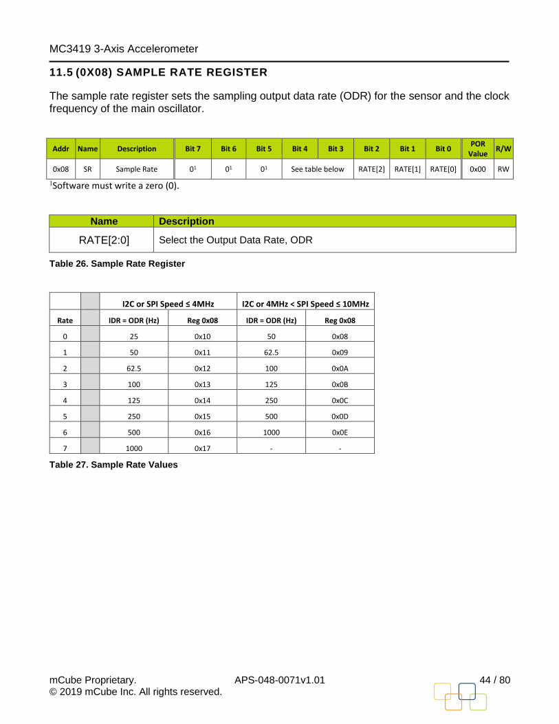
The MC3419 supports eight sample rates using I2C or SPI interfaces. When decimation mode is disabled, the table below shows the “internal data rate” (IDR) which is the same as ODR (ODR = IDR). The sample rate register (0x08) selects the WAKE mode sample rate.
I2C or SPI Speed ≤ 4MHz I2C or 4MHz < SPI Speed ≤ 10MHz
Rate IDR = ODR (Hz) Reg 0x08 IDR = ODR (Hz) Reg 0x08
0 25 0x10 50 0x08
1 50 0x11 62.5 0x09
2 62.5 0x12 100 0x0A
3 100 0x13 125 0x0B
4 125 0x14 250 0x0C
5 250 0x15 500 0x0D
6 500 0x16 1000 0x0E
7 1000 0x17 - -
Table 19. Sample Rate Settings
MC3419 3-Axis Accelerometer
mCube Proprietary. APS-048-0071v1.01 32 / 80 © 2019 mCube Inc. All rights reserved.
9.3 ADDITIONAL RATE OPTIONS
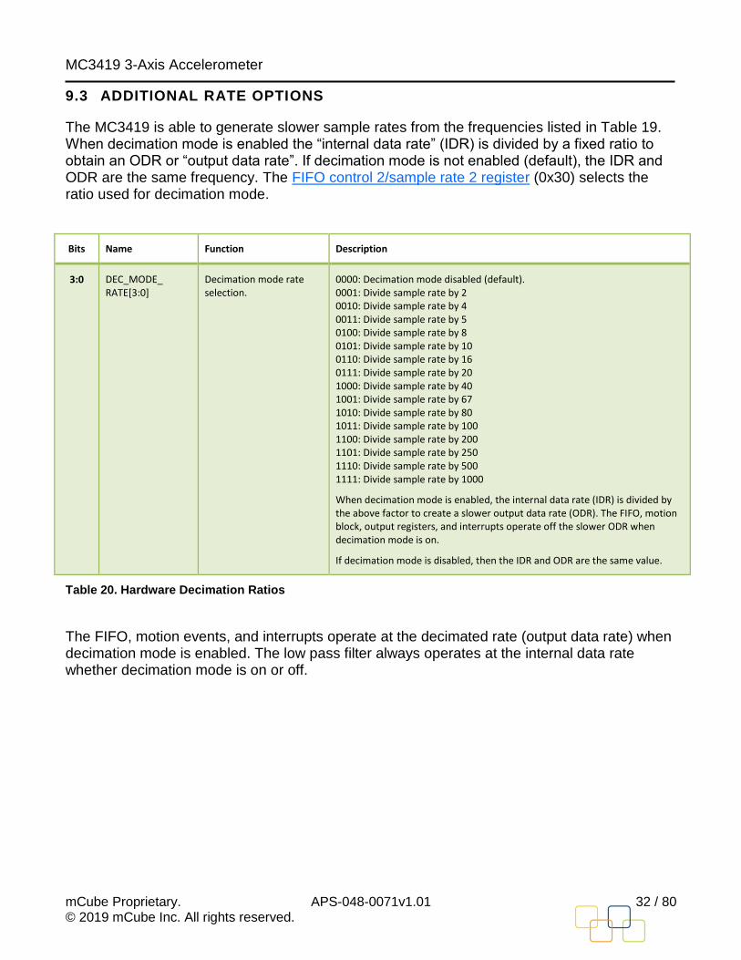
The MC3419 is able to generate slower sample rates from the frequencies listed in Table 19. When decimation mode is enabled the “internal data rate” (IDR) is divided by a fixed ratio to obtain an ODR or “output data rate”. If decimation mode is not enabled (default), the IDR and ODR are the same frequency. The FIFO control 2/sample rate 2 register (0x30) selects the ratio used for decimation mode.
Bits Name Function Description
3:0 DEC_MODE_ RATE[3:0]
Decimation mode rate selection.
0000: Decimation mode disabled (default). 0001: Divide sample rate by 2 0010: Divide sample rate by 4 0011: Divide sample rate by 5 0100: Divide sample rate by 8 0101: Divide sample rate by 10 0110: Divide sample rate by 16 0111: Divide sample rate by 20 1000: Divide sample rate by 40 1001: Divide sample rate by 67 1010: Divide sample rate by 80 1011: Divide sample rate by 100 1100: Divide sample rate by 200 1101: Divide sample rate by 250 1110: Divide sample rate by 500 1111: Divide sample rate by 1000
When decimation mode is enabled, the internal data rate (IDR) is divided by the above factor to create a slower output data rate (ODR). The FIFO, motion block, output registers, and interrupts operate off the slower ODR when decimation mode is on.
If decimation mode is disabled, then the IDR and ODR are the same value.
Table 20. Hardware Decimation Ratios
The FIFO, motion events, and interrupts operate at the decimated rate (output data rate) when decimation mode is enabled. The low pass filter always operates at the internal data rate whether decimation mode is on or off.
MC3419 3-Axis Accelerometer
mCube Proprietary. APS-048-0071v1.01 33 / 80 © 2019 mCube Inc. All rights reserved.
10 I2C INTERFACE
10.1 PHYSICAL INTERFACE
The I2C slave interface operates at a maximum speed of 1 MHz. The SDA (data) is an open-drain, bi-directional pin and the SCL (clock) is an input pin.
Note: The device always operates as an I2C slave.
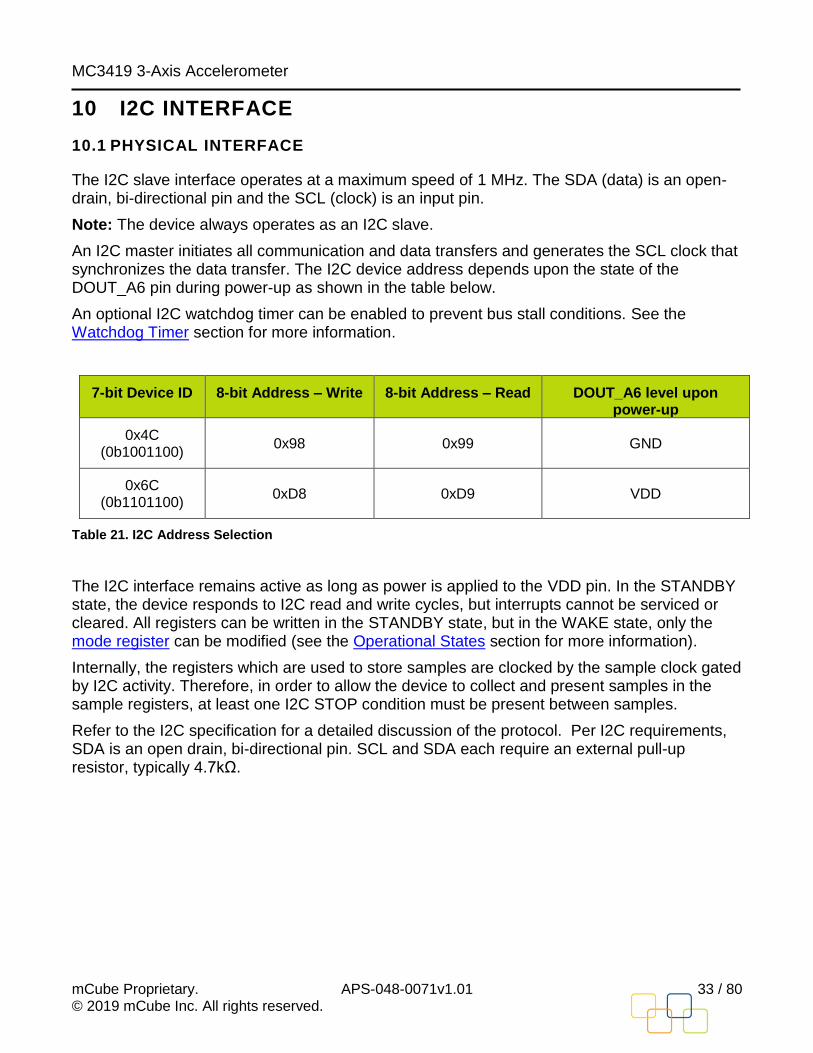
An I2C master initiates all communication and data transfers and generates the SCL clock that synchronizes the data transfer. The I2C device address depends upon the state of the DOUT_A6 pin during power-up as shown in the table below.
An optional I2C watchdog timer can be enabled to prevent bus stall conditions. See the Watchdog Timer section for more information.
7-bit Device ID 8-bit Address – Write 8-bit Address – Read DOUT_A6 level upon power-up
0x4C (0b1001100)
0x98 0x99 GND
0x6C (0b1101100)
0xD8 0xD9 VDD
Table 21. I2C Address Selection
The I2C interface remains active as long as power is applied to the VDD pin. In the STANDBY state, the device responds to I2C read and write cycles, but interrupts cannot be serviced or cleared. All registers can be written in the STANDBY state, but in the WAKE state, only the mode register can be modified (see the Operational States section for more information).
Internally, the registers which are used to store samples are clocked by the sample clock gated by I2C activity. Therefore, in order to allow the device to collect and present samples in the sample registers, at least one I2C STOP condition must be present between samples.
Refer to the I2C specification for a detailed discussion of the protocol. Per I2C requirements, SDA is an open drain, bi-directional pin. SCL and SDA each require an external pull-up resistor, typically 4.7kΩ.
MC3419 3-Axis Accelerometer
mCube Proprietary. APS-048-0071v1.01 34 / 80 © 2019 mCube Inc. All rights reserved.
10.2 TIMING
See the I2C Timing Characteristics section for I2C timing requirements.
10.3 I2C MESSAGE FORMAT
Note: At least one I2C STOP condition must be present between samples in order for the sensor to update the sample data registers.
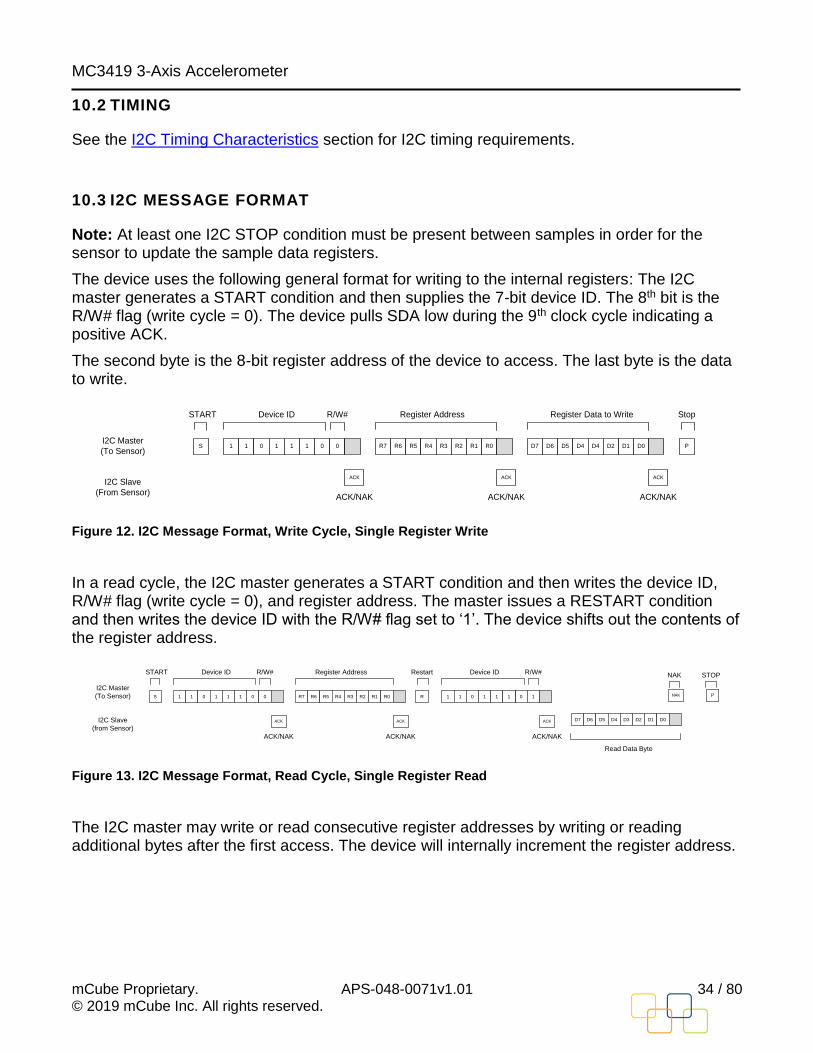
The device uses the following general format for writing to the internal registers: The I2C master generates a START condition and then supplies the 7-bit device ID. The 8th bit is the R/W# flag (write cycle = 0). The device pulls SDA low during the 9th clock cycle indicating a positive ACK.
The second byte is the 8-bit register address of the device to access. The last byte is the data to write.
1 1 0 1 01 1 0
ACK
R7 R6 R5 R4 R1R3 R2 R0 D7 D6 D5 D4 D1D4 D2 D0 PS
ACK ACK
START Device ID R/W#
ACK/NAK
Register Address Register Data to Write Stop
ACK/NAK ACK/NAK
I2C Master
(To Sensor)
I2C Slave
(From Sensor)
Figure 12. I2C Message Format, Write Cycle, Single Register Write
In a read cycle, the I2C master generates a START condition and then writes the device ID, R/W# flag (write cycle = 0), and register address. The master issues a RESTART condition and then writes the device ID with the R/W# flag set to ‘1’. The device shifts out the contents of the register address.
1 1 0 1 01 1 0
ACK
R7 R6 R5 R4 R1R3 R2 R0 RS
ACK
I2C Master
(To Sensor)
I2C Slave
(from Sensor)
START Device ID R/W#
ACK/NAK
Register Address Restart
ACK/NAK
D7 D6 D5 D4 D1D3 D2 D0
NAK
Read Data Byte
NAK
1 1 0 1 01 1 1
ACK
Device ID R/W#
ACK/NAK
P
STOP
Figure 13. I2C Message Format, Read Cycle, Single Register Read
The I2C master may write or read consecutive register addresses by writing or reading additional bytes after the first access. The device will internally increment the register address.
MC3419 3-Axis Accelerometer
mCube Proprietary. APS-048-0071v1.01 35 / 80 © 2019 mCube Inc. All rights reserved.
10.4 I2C WATCHDOG TIMER
The I2C watchdog timer, when enabled (see the mode register), prevents bus stall conditions when the master does not provide enough clocks to the slave to complete a read cycle. The I2C watchdog timer does not resolve why the master did not provide enough clocks to complete a read cycle, but it does prevent a slave from holding the bus indefinitely.
During a read cycle, the slave that is actively driving the bus (SDA pin) does not release the bus until nine SCL clock edges are detected. While the SDA pin is held low by a slave open-drain output, any other I2C devices attached to the bus will not be able to communicate. If the slave does not see nine SCL clocks from the master within the timeout period (about 200 ms), the slave assumes a system problem has occurred and resets the I2C circuitry, releases the SDA pin, and readies the sensor for additional I2C commands.
When an I2C watchdog timer event is triggered, the I2C_WDT bit in the device status register is activated by the Watchdog timer hardware. No other registers are changed. External software can detect this activation by reading the I2C_WDT bit. Reading the device status register (0x05) clears the I2C_WDT bit.
MC3419 3-Axis Accelerometer
mCube Proprietary. APS-048-0071v1.01 36 / 80 © 2019 mCube Inc. All rights reserved.
10.5 SPI PHYSICAL INTERFACE
The device always operates as an SPI slave. An SPI master must initiate all communication and data transfers and generate the SCK_SCL clock that synchronizes the data transfer. The CSN pin must be pulled up to VDD when the SPI interface is not in use. The SPI interface can operate in 3-wire or 4-wire mode. See section 9.2 for SPI clock selection and Output Data Rate, ODR.
10.6 SPI PROTOCOL
An SPI write transaction requires a minimum of 16 clock cycles, and a SPI read transaction requires a minimum of 24 cycles of the SCK_SCL pin. The falling edge of CSN initiates the start of the SPI bus cycle. When the SPI master is writing data to the MC3419 via the SPI DIN pin, data may change when the SCL_SCK is low, and must be stable on the rising edge. Similarly, output data written from MC3419 to the SPI master is shifted out on the SPI DOUT pin on the falling edge of SCL_SCK and can be latched by the master on the rising edge of SCL_SCK. Serial data in or out of the device is always MSB first.
10.7 SPI REGISTER WRITE CYCLE - SINGLE
A single register write consists of a 16-clock transaction. As described above, the first bit is set to ‘0’ indicating a register write followed by the register address.
1 2 3 4 5 6 7 8 9 10 11 12 13 14 15 16
0 A6 A5 A4 A3 A2 A1 A0 DIN7 DIN6 DIN5 DIN4 DIN3 DIN2 DIN1 DIN0
CSN
SCL_SCK
SPI_DIN
SPI_DOUT Z
Figure 14. SPI Register Write Cycle - Single
10.8 SPI REGISTER WRITE CYCLE - BURST
A burst (multi-byte) register write cycle uses the address specified at the beginning of the transaction as the starting register address. Internally the address will auto-increment to the next consecutive address for each additional byte (8-clocks) of data written beyond clock 8.
1 2 3 4 5 6 7 8 9 10 11 12 13 14 15 16 17 18 2219 2120 23 24
0 A6 A5 A4 A3 A2 A1 A0 DIN7 DIN6 DIN5 DIN4 DIN3 DIN2 DIN1 DIN0
CSN
SCL_SCK
DIN_SDA
DOUT_A6
26 3027 2928 31 3225
DIN15 DIN14 DIN13 DIN12 DIN11 DIN10 DIN9 DIN8
Data for register N+1 Data for register N+2
DIN31 DIN30 DIN29 DIN28 DIN27 DIN26 DIN25 DIN24
Data for register N
Figure 15.SPI Register Write Cycle - Burst (3-register burst example)
MC3419 3-Axis Accelerometer
mCube Proprietary. APS-048-0071v1.01 37 / 80 © 2019 mCube Inc. All rights reserved.
10.9 SPI REGISTER READ CYCLE - SINGLE
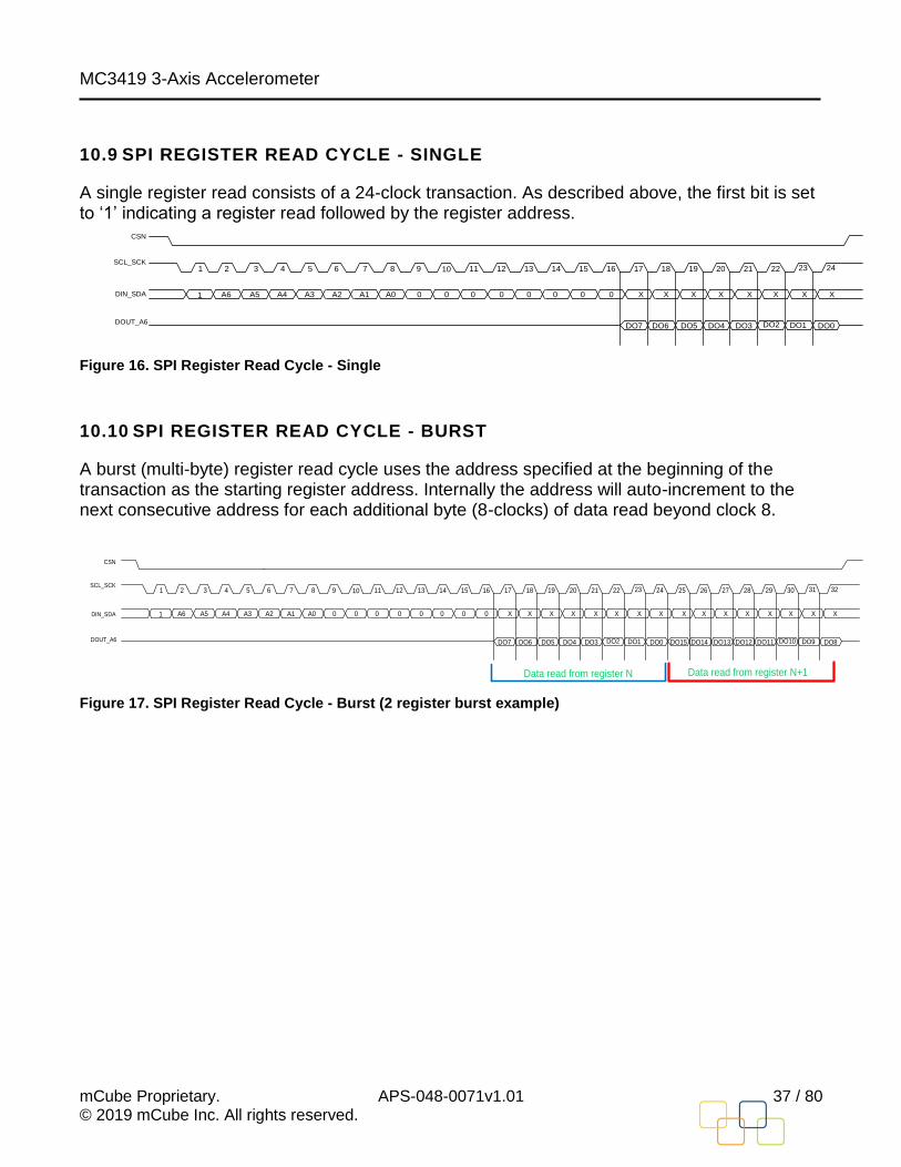
A single register read consists of a 24-clock transaction. As described above, the first bit is set to ‘1’ indicating a register read followed by the register address.
1 2 3 4 5 6 7 8 9 10 11 12 13 14 15 16 17 18 2219 2120 23 24
1 A6 A5 A4 A3 A2 A1 A0 0 00 0 0 0 0 0 X X X X X X X X
DO7 DO6 DO5 DO4 DO3 DO2 DO1 DO0
CSN
SCL_SCK
DIN_SDA
DOUT_A6
Figure 16. SPI Register Read Cycle - Single
10.10 SPI REGISTER READ CYCLE - BURST
A burst (multi-byte) register read cycle uses the address specified at the beginning of the transaction as the starting register address. Internally the address will auto-increment to the next consecutive address for each additional byte (8-clocks) of data read beyond clock 8.
1 2 3 4 5 6 7 8 9 10 11 12 13 14 15 16 17 18 2219 2120 23
1 A6 A5 A4 A3 A2 A1 A0 0 00 0 0 0 0 0 X X X X X X X X
DO7 DO6 DO5 DO4 DO3 DO2 DO1 DO0
25 26 3027 2928 31 32
X X X X X X X X
DO15 DO14 DO13 DO12 DO11 DO10 DO9 DO8
24
CSN
SCL_SCK
DIN_SDA
DOUT_A6
Data read from register N Data read from register N+1
Figure 17. SPI Register Read Cycle - Burst (2 register burst example)
MC3419 3-Axis Accelerometer
mCube Proprietary. APS-048-0071v1.01 38 / 80 © 2019 mCube Inc. All rights reserved.
11 REGISTER INTERFACE
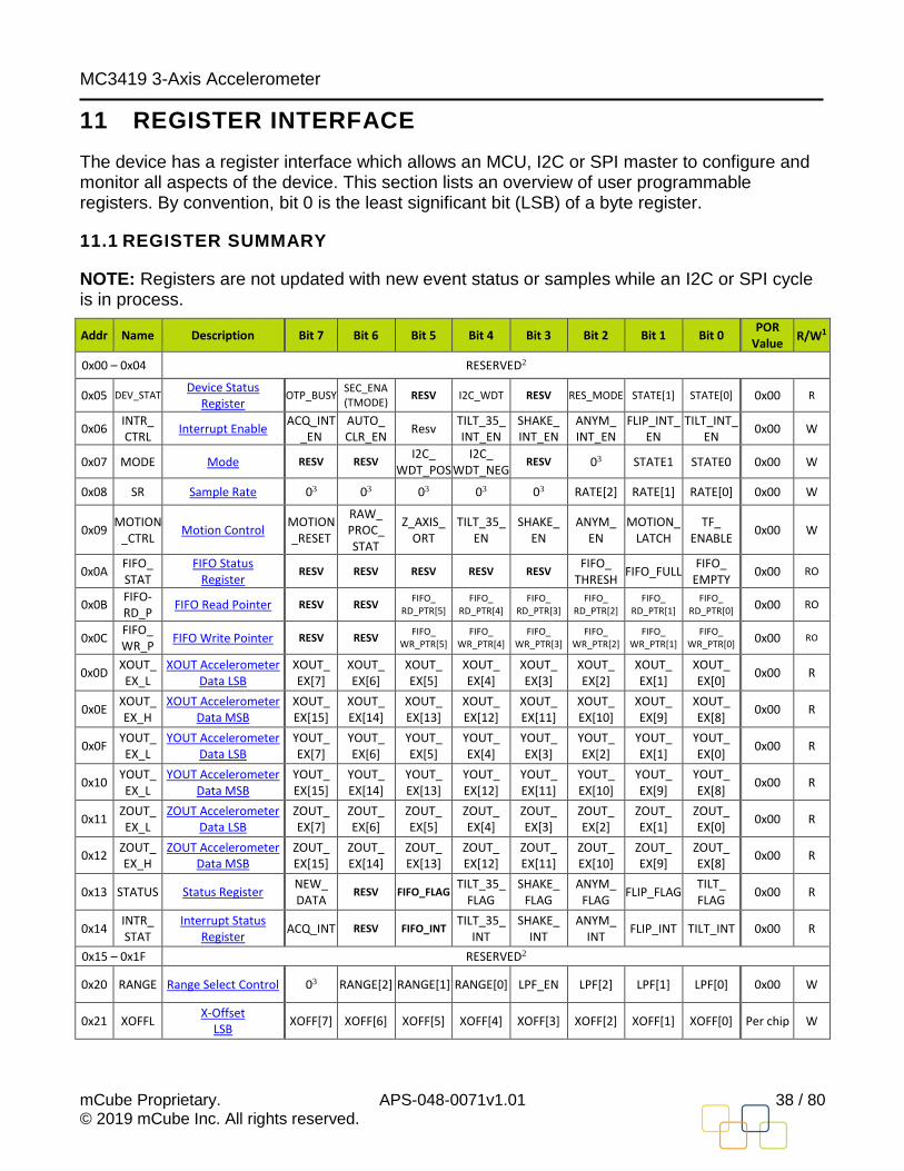
The device has a register interface which allows an MCU, I2C or SPI master to configure and monitor all aspects of the device. This section lists an overview of user programmable registers. By convention, bit 0 is the least significant bit (LSB) of a byte register.
11.1 REGISTER SUMMARY
NOTE: Registers are not updated with new event status or samples while an I2C or SPI cycle is in process.
Addr Name Description Bit 7 Bit 6 Bit 5 Bit 4 Bit 3 Bit 2 Bit 1 Bit 0 POR
Value R/W1
0x00 – 0x04 RESERVED2
0x05 DEV_STAT Device Status
Register OTP_BUSY
SEC_ENA (TMODE)
RESV I2C_WDT RESV RES_MODE STATE[1] STATE[0] 0x00 R
0x06 INTR_ CTRL
Interrupt Enable
ACQ_INT_EN
AUTO_ CLR_EN
Resv TILT_35_ INT_EN
SHAKE_ INT_EN
ANYM_ INT_EN
FLIP_INT_EN
TILT_INT_EN
0x00 W
0x07 MODE Mode RESV RESV
I2C_ WDT_POS
I2C_ WDT_NEG
RESV 03 STATE1 STATE0 0x00 W
0x08 SR Sample Rate 03 03 03 03 03 RATE[2] RATE[1] RATE[0] 0x00 W
0x09 MOTION
_CTRL Motion Control
MOTION_RESET
RAW_ PROC_ STAT
Z_AXIS_ ORT
TILT_35_ EN
SHAKE_ EN
ANYM_ EN
MOTION_LATCH
TF_ ENABLE
0x00 W
0x0A FIFO_ STAT
FIFO Status Register
RESV RESV RESV RESV RESV FIFO_
THRESH FIFO_FULL
FIFO_ EMPTY
0x00 RO
0x0B FIFO-RD_P
FIFO Read Pointer RESV RESV FIFO_
RD_PTR[5] FIFO_
RD_PTR[4] FIFO_
RD_PTR[3] FIFO_
RD_PTR[2] FIFO_
RD_PTR[1] FIFO_
RD_PTR[0] 0x00 RO
0x0C FIFO_ WR_P
FIFO Write Pointer RESV RESV FIFO_
WR_PTR[5] FIFO_
WR_PTR[4] FIFO_
WR_PTR[3] FIFO_
WR_PTR[2] FIFO_
WR_PTR[1] FIFO_
WR_PTR[0] 0x00 RO
0x0D XOUT_ EX_L
XOUT Accelerometer Data LSB
XOUT_ EX[7]
XOUT_ EX[6]
XOUT_ EX[5]
XOUT_ EX[4]
XOUT_ EX[3]
XOUT_ EX[2]
XOUT_ EX[1]
XOUT_ EX[0]
0x00 R
0x0E XOUT_ EX_H
XOUT Accelerometer Data MSB
XOUT_ EX[15]
XOUT_ EX[14]
XOUT_ EX[13]
XOUT_ EX[12]
XOUT_ EX[11]
XOUT_ EX[10]
XOUT_ EX[9]
XOUT_ EX[8]
0x00 R
0x0F YOUT_ EX_L
YOUT Accelerometer Data LSB
YOUT_ EX[7]
YOUT_ EX[6]
YOUT_ EX[5]
YOUT_ EX[4]
YOUT_ EX[3]
YOUT_ EX[2]
YOUT_ EX[1]
YOUT_ EX[0]
0x00 R
0x10 YOUT_ EX_L
YOUT Accelerometer Data MSB
YOUT_ EX[15]
YOUT_ EX[14]
YOUT_ EX[13]
YOUT_ EX[12]
YOUT_ EX[11]
YOUT_ EX[10]
YOUT_ EX[9]
YOUT_ EX[8]
0x00 R
0x11 ZOUT_ EX_L
ZOUT Accelerometer Data LSB
ZOUT_ EX[7]
ZOUT_ EX[6]
ZOUT_ EX[5]
ZOUT_ EX[4]
ZOUT_ EX[3]
ZOUT_ EX[2]
ZOUT_ EX[1]
ZOUT_ EX[0]
0x00 R
0x12 ZOUT_ EX_H
ZOUT Accelerometer Data MSB
ZOUT_ EX[15]
ZOUT_ EX[14]
ZOUT_ EX[13]
ZOUT_ EX[12]
ZOUT_ EX[11]
ZOUT_ EX[10]
ZOUT_ EX[9]
ZOUT_ EX[8]
0x00 R
0x13 STATUS Status Register
NEW_ DATA
RESV FIFO_FLAG TILT_35_
FLAG SHAKE_
FLAG ANYM_
FLAG FLIP_FLAG
TILT_ FLAG
0x00 R
0x14 INTR_ STAT
Interrupt Status Register
ACQ_INT RESV FIFO_INT TILT_35_
INT SHAKE_
INT ANYM_
INT FLIP_INT TILT_INT 0x00 R
0x15 – 0x1F RESERVED2
0x20 RANGE Range Select Control 03 RANGE[2] RANGE[1] RANGE[0] LPF_EN LPF[2] LPF[1] LPF[0] 0x00 W
0x21 XOFFL X-Offset
LSB
XOFF[7] XOFF[6] XOFF[5] XOFF[4] XOFF[3] XOFF[2] XOFF[1] XOFF[0] Per chip W

MC3419 3-Axis Accelerometer
mCube Proprietary. APS-048-0071v1.01 39 / 80 © 2019 mCube Inc. All rights reserved.
Addr Name Description Bit 7 Bit 6 Bit 5 Bit 4 Bit 3 Bit 2 Bit 1 Bit 0 POR
Value R/W1
0x22 XOFFH X-Offset
MSB
XGAIN[8] XOFF[14] XOFF[13] XOFF[12] XOFF[11] XOFF[10] XOFF[9] XOFF[8] Per chip W
0x23 YOFFL Y-Offset
LSB
YOFF[7] YOFF[6] YOFF[5] YOFF[4] YOFF[3] YOFF[2] YOFF[1] YOFF[0] Per chip W
I0x24 YOFFH Y-Offset
MSB
YGAIN[8] YOFF[14] YOFF[13] YOFF[12] YOFF[11] YOFF[10] YOFF[9] YOFF[8] Per chip W
0x25 ZOFFL Z-Offset
LSB
ZOFF[7] ZOFF[6] ZOFF[5] ZOFF[4] ZOFF[3] ZOFF[2] ZOFF[1] ZOFF[0] Per chip W
0x26 ZOFFH Z-Offset
MSB
ZGAIN[8] ZOFF[14] ZOFF[13] ZOFF[12] ZOFF[11] ZOFF[10] ZOFF[9] ZOFF[8] Per chip W
0x27 XGAIN X Gain XGAIN[7] XGAIN[6] XGAIN[5] XGAIN[4] XGAIN[3] XGAIN[2] XGAIN[1] XGAIN[0] Per chip W
0x28 YGAIN Y Gain YGAIN[7] YGAIN[6] YGAIN[5] YGAIN[4] YGAIN[3] YGAIN[2] YGAIN[1] YGAIN[0] Per chip W
0x29 ZGAIN Z Gain ZGAIN[7] ZGAIN[6] ZGAIN[5] ZGAIN[4] ZGAIN[3] ZGAIN[2] ZGAIN[1] ZGAIN[0] Per chip W
0x2A -0x2C RESERVED2
0x2D FIFO_ CTRL
FIFO Control Register 03 FIFO_ MODE
FIFO_EN FIFO_RESET COMB_INT
_ EN FIFO_TH_
INT_EN FIFO_FULL_
INT_EN
FIFO_ EMPTY_ INT_EN
0x00 W
0x2E FIFO_TH FIFO Threshold
Register RESV RESV RESV FIFO_TH[4] FIFO_TH[3] FIFO_TH[2] FIFO_TH[1] FIFO_TH[0] 0x10 W
0x2F FIFO_ INTR
FIFO Interrupt Status Register
03 RESV RESV RESV RESV FIFO_
THRESH_ INT (RO)
FIFO_FULL_ INT (RO)
FIFO_EMPTY _INT (RO)
0x00 R W
0x30 FIFO_ CTRL2 _SR2
FIFO Control 2, Sample Rate 2
Register
FIFO_ BURST_ MODE
03
SELECT_ WRAP_ ADDR
ENABLE_ WRAP_N
DEC_MODE RATE[3]
DEC_ MODE
RATE[2]
DEC_MODE RATE[1]
DEC_MODE RATE[0]
0x00 W
0x31 COMM_
CTRL Comm. Control
Register 03
INDIV_ INTR_CLR
SPI_3WIRE_ EN
INT1_INT2_ REQ_SWAP
I2C_FILTER_ MAN
I2C_FILTER _EN
RESV RESV 0x00 W
0x32 RESERVED2
0x33 GPIO_ CTRL
GPIO Control Register
INTN2_ IPP
INTN2_IAH RESV RESV INTN1_
IPP INTN1_IAH RESV RESV 0x00 W
0x34 -0x3F RESERVED2
0x40 TF_
THRESH_LSB
Tilt/Flip Threshold LSB
TF_ THR[7]
TF_THR[6] TF_THR[5] TF_THR[4] TF_THR[3] TF_THR[2] TF_THR[1] TF_
THR[0] 0x00 W
0x41 TF_
THRESH_MSB
Tilt/Flip Threshold MSB
RESV TF_
THR[14] TF_
THR[13] TF_
THR[12] TF_
THR[11] TF_
THR[10] TF_THR[9]
TF_ THR[8]
0x00 W
0x42 TF_DB Tilt/Flip Debounce TF_DB[7] TF_DB[6] TF_DB[5] TF_DB[4] TF_DB[3] TF_DB[2] TF_DB[1] TF_DB[0] 0x00 W
0x43 AM_
THRESH_LSB
AnyMotion Threshold LSB
ANYM_ THR[7]
ANYM_ THR[6]
ANYM_ THR[5]
ANYM_ THR[4]
ANYM_ THR[3]
ANYM_ THR[2]
ANYM_ THR[1]
ANYM_ THR[0]
0x00 W
0x44 AM_
THRESH_MSB
AnyMotion Threshold MSB
RESV ANYM_ THR[14]
ANYM_ THR[13]
ANYM_ THR[12]
ANYM_ THR[11]
ANYM_ THR[10]
ANYM_ THR[9]
ANYM_ THR[8]
0x00 W
0x45 AM_DB AnyMotion Debounce
ANYM_ DB[7]
ANYM_ DB[6]
ANYM_ DB[5]
ANYM_ DB[4]
ANYM_ DB[3]
ANYM_ DB[2]
ANYM_ DB[1]
ANYM_ DB[0]
0x00 W
0x46 SHK_
THRESH_LSB
Shake Threshold LSB
SH _ THR[7]
SH _ THR[6]
SH _ THR[5]
SH _ THR[4]
SH _ THR[3]
SH _ THR[2]
SH _ THR[1]
SH _ THR[0]
0x00 W
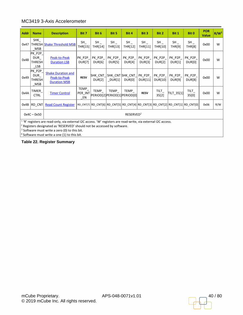
MC3419 3-Axis Accelerometer
mCube Proprietary. APS-048-0071v1.01 40 / 80 © 2019 mCube Inc. All rights reserved.
Addr Name Description Bit 7 Bit 6 Bit 5 Bit 4 Bit 3 Bit 2 Bit 1 Bit 0 POR
Value R/W1
0x47 SHK_
THRESH_MSB
Shake Threshold MSB
SH_ THR[15]
SH _ THR[14]
SH _ THR[13]
SH _ THR[12]
SH _ THR[11]
SH _ THR[10]
SH _ THR[9]
SH _ THR[8]
0x00 W
0x48
PK_P2P_DUR_
THRESH_LSB
Peak-to-Peak Duration LSB
PK_P2P_ DUR[7]
PK_P2P_ DUR[6]
PK_P2P_ DUR[5]
PK_P2P_ DUR[4]
PK_P2P_ DUR[3]
PK_P2P_ DUR[2]
PK_P2P_ DUR[1]
PK_P2P_ DUR[0]
0x00 W
0x49
PK_P2P_DUR_
THRESH_MSB
Shake Duration and Peak-to-Peak Duration MSB
RESV SHK_CNT_
DUR[2] SHK_CNT_DUR[1]
SHK_CNT_DUR[0]
PK_P2P_ DUR[11]
PK_P2P_ DUR[10]
PK_P2P_ DUR[9]
PK_P2P_ DUR[8]
0x00 W
0x4A TIMER_
CTRL Timer Control
TEMP_ PER_INT
_EN
TEMP_ PERIOD[2]
TEMP_ PERIOD[1]
TEMP_ PERIOD[0]
RESV TILT_ 35[2]
TILT_35[1] TILT_ 35[0]
0x00 W
0x4B RD_CNT Read Count Register RD_CNT[7] RD_CNT[6] RD_CNT[5] RD_CNT[4] RD_CNT[3] RD_CNT[2] RD_CNT[1] RD_CNT[0] 0x06 R/W
0x4C – 0x50 RESERVED2
1 ‘R’ registers are read-only, via external I2C access. ‘W’ registers are read-write, via external I2C access. 2 Registers designated as ‘RESERVED’ should not be accessed by software. 3 Software must write a zero (0) to this bit. 4 Software must write a one (1) to this bit.
Table 22. Register Summary
MC3419 3-Axis Accelerometer
mCube Proprietary. APS-048-0071v1.01 41 / 80 © 2019 mCube Inc. All rights reserved.
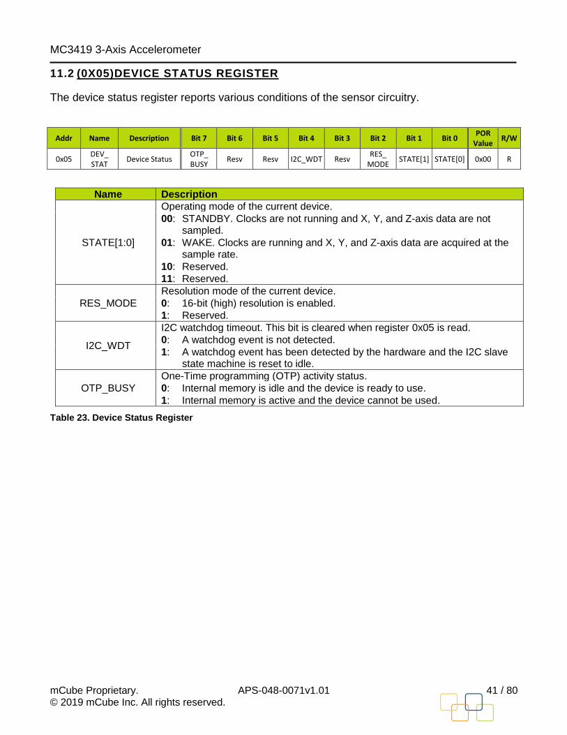
11.2 (0X05)DEVICE STATUS REGISTER
The device status register reports various conditions of the sensor circuitry.
Addr Name Description Bit 7 Bit 6 Bit 5 Bit 4 Bit 3 Bit 2 Bit 1 Bit 0 POR
Value R/W
0x05 DEV_ STAT
Device Status OTP_ BUSY
Resv Resv I2C_WDT Resv RES_
MODE STATE[1] STATE[0] 0x00 R
Name Description
STATE[1:0]
Operating mode of the current device.
00: STANDBY. Clocks are not running and X, Y, and Z-axis data are not sampled.
01: WAKE. Clocks are running and X, Y, and Z-axis data are acquired at the sample rate.
10: Reserved.
11: Reserved.
RES_MODE
Resolution mode of the current device.
0: 16-bit (high) resolution is enabled.
1: Reserved.
I2C_WDT
I2C watchdog timeout. This bit is cleared when register 0x05 is read.
0: A watchdog event is not detected.
1: A watchdog event has been detected by the hardware and the I2C slave state machine is reset to idle.
OTP_BUSY
One-Time programming (OTP) activity status.
0: Internal memory is idle and the device is ready to use.
1: Internal memory is active and the device cannot be used.
Table 23. Device Status Register
MC3419 3-Axis Accelerometer
mCube Proprietary. APS-048-0071v1.01 42 / 80 © 2019 mCube Inc. All rights reserved.
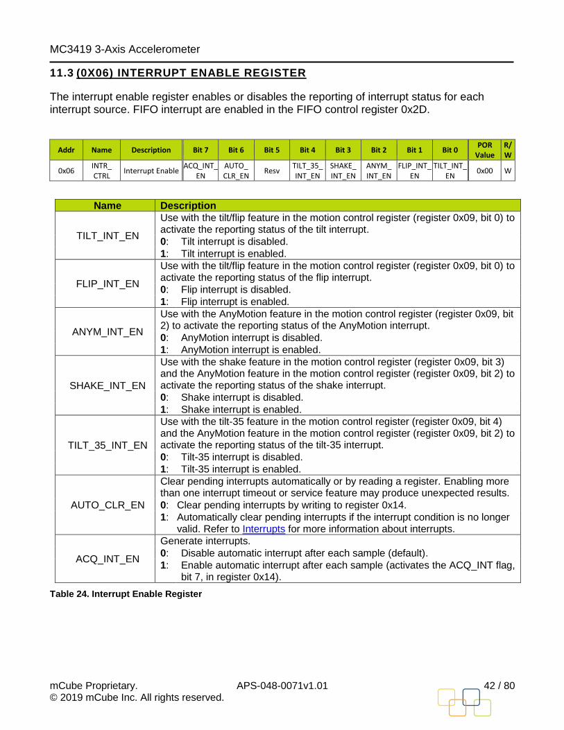
11.3 (0X06) INTERRUPT ENABLE REGISTER
The interrupt enable register enables or disables the reporting of interrupt status for each interrupt source. FIFO interrupt are enabled in the FIFO control register 0x2D.
Addr Name Description Bit 7 Bit 6 Bit 5 Bit 4 Bit 3 Bit 2 Bit 1 Bit 0 POR
Value R/W
0x06 INTR_ CTRL
Interrupt Enable ACQ_INT_
EN AUTO_ CLR_EN
Resv TILT_35_ INT_EN
SHAKE_ INT_EN
ANYM_ INT_EN
FLIP_INT_EN
TILT_INT_EN
0x00 W
Name Description
TILT_INT_EN
Use with the tilt/flip feature in the motion control register (register 0x09, bit 0) to activate the reporting status of the tilt interrupt.
0: Tilt interrupt is disabled.
1: Tilt interrupt is enabled.
FLIP_INT_EN
Use with the tilt/flip feature in the motion control register (register 0x09, bit 0) to activate the reporting status of the flip interrupt.
0: Flip interrupt is disabled.
1: Flip interrupt is enabled.
ANYM_INT_EN
Use with the AnyMotion feature in the motion control register (register 0x09, bit 2) to activate the reporting status of the AnyMotion interrupt.
0: AnyMotion interrupt is disabled.
1: AnyMotion interrupt is enabled.
SHAKE_INT_EN
Use with the shake feature in the motion control register (register 0x09, bit 3) and the AnyMotion feature in the motion control register (register 0x09, bit 2) to activate the reporting status of the shake interrupt.
0: Shake interrupt is disabled.
1: Shake interrupt is enabled.
TILT_35_INT_EN
Use with the tilt-35 feature in the motion control register (register 0x09, bit 4) and the AnyMotion feature in the motion control register (register 0x09, bit 2) to activate the reporting status of the tilt-35 interrupt.
0: Tilt-35 interrupt is disabled.
1: Tilt-35 interrupt is enabled.
AUTO_CLR_EN
Clear pending interrupts automatically or by reading a register. Enabling more than one interrupt timeout or service feature may produce unexpected results.
0: Clear pending interrupts by writing to register 0x14.
1: Automatically clear pending interrupts if the interrupt condition is no longer valid. Refer to Interrupts for more information about interrupts.
ACQ_INT_EN
Generate interrupts.
0: Disable automatic interrupt after each sample (default).
1: Enable automatic interrupt after each sample (activates the ACQ_INT flag, bit 7, in register 0x14).
Table 24. Interrupt Enable Register
MC3419 3-Axis Accelerometer
mCube Proprietary. APS-048-0071v1.01 43 / 80 © 2019 mCube Inc. All rights reserved.
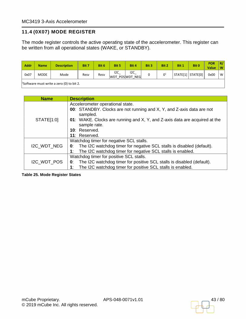
11.4 (0X07) MODE REGISTER
The mode register controls the active operating state of the accelerometer. This register can be written from all operational states (WAKE, or STANDBY).
Addr Name Description Bit 7 Bit 6 Bit 5 Bit 4 Bit 3 Bit 2 Bit 1 Bit 0 POR
Value R/W
0x07 MODE Mode Resv Resv I2C_
WDT_POS I2C_
WDT_NEG 0 01 STATE[1] STATE[0] 0x00 W
1Software must write a zero (0) to bit 2.
Name Description
STATE[1:0]
Accelerometer operational state.
00: STANDBY. Clocks are not running and X, Y, and Z-axis data are not sampled.
01: WAKE. Clocks are running and X, Y, and Z-axis data are acquired at the sample rate.
10: Reserved.
11: Reserved.
I2C_WDT_NEG
Watchdog timer for negative SCL stalls.
0: The I2C watchdog timer for negative SCL stalls is disabled (default).
1: The I2C watchdog timer for negative SCL stalls is enabled.
I2C_WDT_POS
Watchdog timer for positive SCL stalls.
0: The I2C watchdog timer for positive SCL stalls is disabled (default).
1: The I2C watchdog timer for positive SCL stalls is enabled.
Table 25. Mode Register States
MC3419 3-Axis Accelerometer
mCube Proprietary. APS-048-0071v1.01 44 / 80 © 2019 mCube Inc. All rights reserved.
11.5 (0X08) SAMPLE RATE REGISTER
The sample rate register sets the sampling output data rate (ODR) for the sensor and the clock frequency of the main oscillator.
Addr Name Description Bit 7 Bit 6 Bit 5 Bit 4 Bit 3 Bit 2 Bit 1 Bit 0 POR
Value R/W
0x08 SR Sample Rate 01 01 01 See table below RATE[2] RATE[1] RATE[0] 0x00 RW
1Software must write a zero (0).
Name Description
RATE[2:0] Select the Output Data Rate, ODR
Table 26. Sample Rate Register
I2C or SPI Speed ≤ 4MHz I2C or 4MHz < SPI Speed ≤ 10MHz
Rate IDR = ODR (Hz) Reg 0x08 IDR = ODR (Hz) Reg 0x08
0 25 0x10 50 0x08
1 50 0x11 62.5 0x09
2 62.5 0x12 100 0x0A
3 100 0x13 125 0x0B
4 125 0x14 250 0x0C
5 250 0x15 500 0x0D
6 500 0x16 1000 0x0E
7 1000 0x17 - -
Table 27. Sample Rate Values
MC3419 3-Axis Accelerometer
mCube Proprietary. APS-048-0071v1.01 45 / 80 © 2019 mCube Inc. All rights reserved.
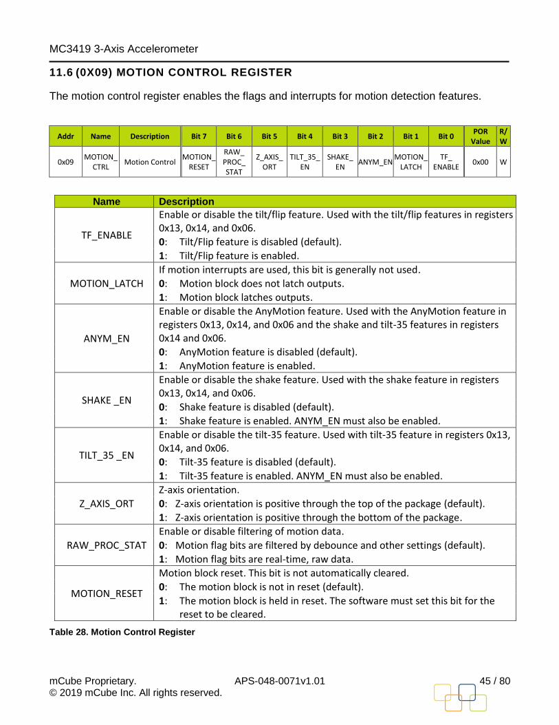
11.6 (0X09) MOTION CONTROL REGISTER
The motion control register enables the flags and interrupts for motion detection features.
Addr Name Description Bit 7 Bit 6 Bit 5 Bit 4 Bit 3 Bit 2 Bit 1 Bit 0 POR
Value R/W
0x09 MOTION_
CTRL Motion Control
MOTION_RESET
RAW_ PROC_ STAT
Z_AXIS_ ORT
TILT_35_ EN
SHAKE_ EN
ANYM_EN MOTION_
LATCH TF_
ENABLE 0x00 W
Name Description
TF_ENABLE
Enable or disable the tilt/flip feature. Used with the tilt/flip features in registers 0x13, 0x14, and 0x06.
0: Tilt/Flip feature is disabled (default).
1: Tilt/Flip feature is enabled.
MOTION_LATCH
If motion interrupts are used, this bit is generally not used.
0: Motion block does not latch outputs.
1: Motion block latches outputs.
ANYM_EN
Enable or disable the AnyMotion feature. Used with the AnyMotion feature in registers 0x13, 0x14, and 0x06 and the shake and tilt-35 features in registers 0x14 and 0x06.
0: AnyMotion feature is disabled (default).
1: AnyMotion feature is enabled.
SHAKE _EN
Enable or disable the shake feature. Used with the shake feature in registers 0x13, 0x14, and 0x06.
0: Shake feature is disabled (default).
1: Shake feature is enabled. ANYM_EN must also be enabled.
TILT_35 _EN
Enable or disable the tilt-35 feature. Used with tilt-35 feature in registers 0x13, 0x14, and 0x06.
0: Tilt-35 feature is disabled (default).
1: Tilt-35 feature is enabled. ANYM_EN must also be enabled.
Z_AXIS_ORT
Z-axis orientation.
0: Z-axis orientation is positive through the top of the package (default).
1: Z-axis orientation is positive through the bottom of the package.
RAW_PROC_STAT
Enable or disable filtering of motion data.
0: Motion flag bits are filtered by debounce and other settings (default).
1: Motion flag bits are real-time, raw data.
MOTION_RESET
Motion block reset. This bit is not automatically cleared.
0: The motion block is not in reset (default).
1: The motion block is held in reset. The software must set this bit for the reset to be cleared.
Table 28. Motion Control Register
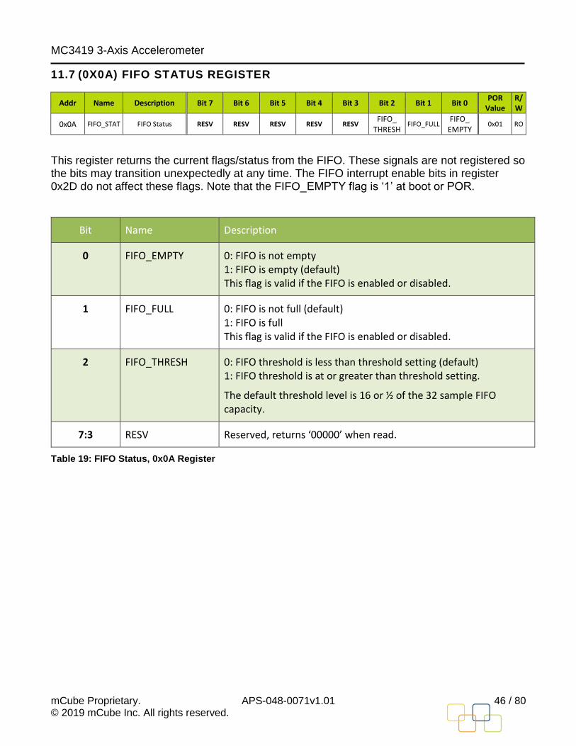
MC3419 3-Axis Accelerometer
mCube Proprietary. APS-048-0071v1.01 46 / 80 © 2019 mCube Inc. All rights reserved.
11.7 (0X0A) FIFO STATUS REGISTER
Addr Name Description Bit 7 Bit 6 Bit 5 Bit 4 Bit 3 Bit 2 Bit 1 Bit 0 POR
Value R/W
0x0A FIFO_STAT FIFO Status RESV RESV RESV RESV RESV FIFO_
THRESH FIFO_FULL
FIFO_ EMPTY
0x01 RO
This register returns the current flags/status from the FIFO. These signals are not registered so the bits may transition unexpectedly at any time. The FIFO interrupt enable bits in register 0x2D do not affect these flags. Note that the FIFO_EMPTY flag is ‘1’ at boot or POR.
Bit Name Description
0 FIFO_EMPTY 0: FIFO is not empty 1: FIFO is empty (default) This flag is valid if the FIFO is enabled or disabled.
1 FIFO_FULL 0: FIFO is not full (default) 1: FIFO is full This flag is valid if the FIFO is enabled or disabled.
2 FIFO_THRESH 0: FIFO threshold is less than threshold setting (default) 1: FIFO threshold is at or greater than threshold setting.
The default threshold level is 16 or ½ of the 32 sample FIFO capacity.
7:3 RESV Reserved, returns ‘00000’ when read.
Table 19: FIFO Status, 0x0A Register
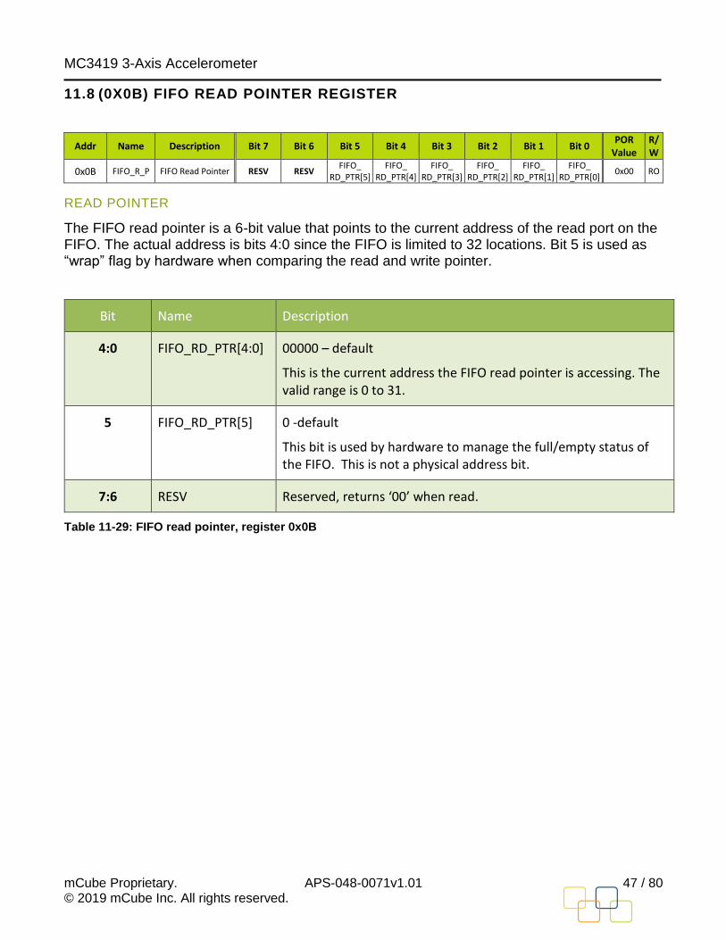
MC3419 3-Axis Accelerometer
mCube Proprietary. APS-048-0071v1.01 47 / 80 © 2019 mCube Inc. All rights reserved.
11.8 (0X0B) FIFO READ POINTER REGISTER
Addr Name Description Bit 7 Bit 6 Bit 5 Bit 4 Bit 3 Bit 2 Bit 1 Bit 0 POR
Value R/W
0x0B FIFO_R_P FIFO Read Pointer RESV RESV FIFO_
RD_PTR[5] FIFO_
RD_PTR[4] FIFO_
RD_PTR[3] FIFO_
RD_PTR[2] FIFO_
RD_PTR[1] FIFO_
RD_PTR[0] 0x00 RO
READ POINTER
The FIFO read pointer is a 6-bit value that points to the current address of the read port on the FIFO. The actual address is bits 4:0 since the FIFO is limited to 32 locations. Bit 5 is used as “wrap” flag by hardware when comparing the read and write pointer.
Bit Name Description
4:0 FIFO_RD_PTR[4:0] 00000 – default
This is the current address the FIFO read pointer is accessing. The valid range is 0 to 31.
5 FIFO_RD_PTR[5] 0 -default
This bit is used by hardware to manage the full/empty status of the FIFO. This is not a physical address bit.
7:6 RESV Reserved, returns ‘00’ when read.
Table 11-29: FIFO read pointer, register 0x0B
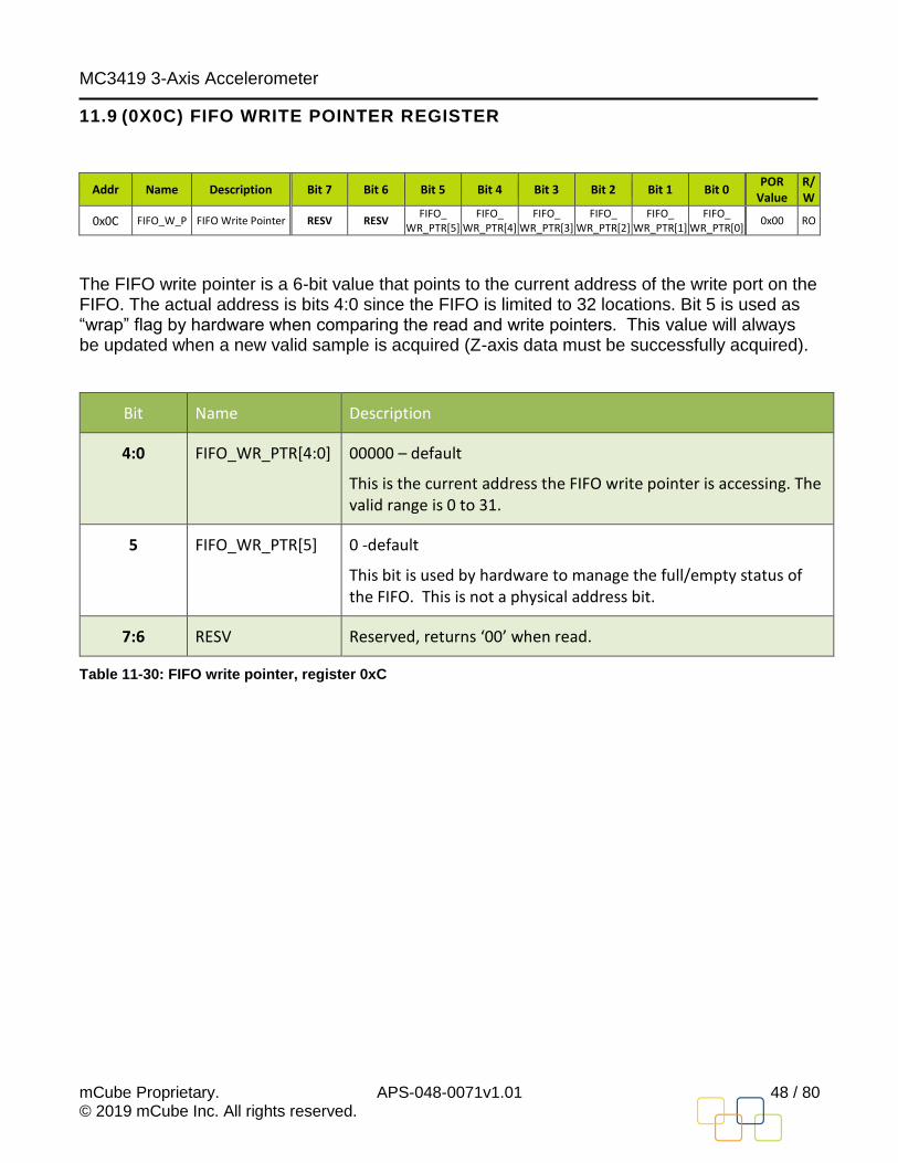
MC3419 3-Axis Accelerometer
mCube Proprietary. APS-048-0071v1.01 48 / 80 © 2019 mCube Inc. All rights reserved.
11.9 (0X0C) FIFO WRITE POINTER REGISTER
Addr Name Description Bit 7 Bit 6 Bit 5 Bit 4 Bit 3 Bit 2 Bit 1 Bit 0 POR
Value R/W
0x0C FIFO_W_P FIFO Write Pointer RESV RESV FIFO_
WR_PTR[5] FIFO_
WR_PTR[4] FIFO_
WR_PTR[3] FIFO_
WR_PTR[2] FIFO_
WR_PTR[1] FIFO_
WR_PTR[0] 0x00 RO
The FIFO write pointer is a 6-bit value that points to the current address of the write port on the FIFO. The actual address is bits 4:0 since the FIFO is limited to 32 locations. Bit 5 is used as “wrap” flag by hardware when comparing the read and write pointers. This value will always be updated when a new valid sample is acquired (Z-axis data must be successfully acquired).
Bit Name Description
4:0 FIFO_WR_PTR[4:0] 00000 – default
This is the current address the FIFO write pointer is accessing. The valid range is 0 to 31.
5 FIFO_WR_PTR[5] 0 -default
This bit is used by hardware to manage the full/empty status of the FIFO. This is not a physical address bit.
7:6 RESV Reserved, returns ‘00’ when read.
Table 11-30: FIFO write pointer, register 0xC
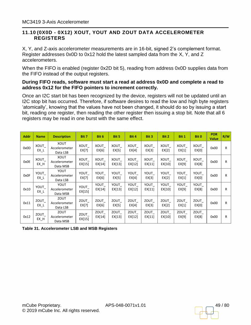
MC3419 3-Axis Accelerometer
mCube Proprietary. APS-048-0071v1.01 49 / 80 © 2019 mCube Inc. All rights reserved.
11.10 (0X0D - 0X12) XOUT, YOUT AND ZOUT DATA ACCELEROMETER REGISTERS
X, Y, and Z-axis accelerometer measurements are in 16-bit, signed 2’s complement format. Register addresses 0x0D to 0x12 hold the latest sampled data from the X, Y, and Z accelerometers.
When the FIFO is enabled (register 0x2D bit 5), reading from address 0x0D supplies data from the FIFO instead of the output registers.
During FIFO reads, software must start a read at address 0x0D and complete a read to address 0x12 for the FIFO pointers to increment correctly.
Once an I2C start bit has been recognized by the device, registers will not be updated until an I2C stop bit has occurred. Therefore, if software desires to read the low and high byte registers ‘atomically’, knowing that the values have not been changed, it should do so by issuing a start bit, reading one register, then reading the other register then issuing a stop bit. Note that all 6 registers may be read in one burst with the same effect.
Addr Name Description Bit 7 Bit 6 Bit 5 Bit 4 Bit 3 Bit 2 Bit 1 Bit 0 POR
Value R/W
0x0D XOUT_
EX_L
XOUT Accelerometer
Data LSB
XOUT_ EX[7]
XOUT_ EX[6]
XOUT_ EX[5]
XOUT_ EX[4]
XOUT_ EX[3]
XOUT_ EX[2]
XOUT_ EX[1]
XOUT_ EX[0]
0x00 R
0x0E XOUT_ EX_H
XOUT Accelerometer
Data MSB
XOUT_ EX[15]
XOUT_ EX[14]
XOUT_ EX[13]
XOUT_ EX[12]
XOUT_ EX[11]
XOUT_ EX[10]
XOUT_ EX[9]
XOUT_ EX[8]
0x00 R
0x0F YOUT_ EX_L
YOUT Accelerometer
Data LSB
YOUT_ EX[7]
YOUT_ EX[6]
YOUT_ EX[5]
YOUT_ EX[4]
YOUT_ EX[3]
YOUT_ EX[2]
YOUT_ EX[1]
YOUT_ EX[0]
0x00 R
0x10 YOUT_ EX_L
YOUT Accelerometer
Data MSB
YOUT_ EX[15]
YOUT_ EX[14]
YOUT_ EX[13]
YOUT_ EX[12]
YOUT_ EX[11]
YOUT_ EX[10]
YOUT_ EX[9]
YOUT_ EX[8] 0x00 R
0x11 ZOUT_ EX_L
ZOUT Accelerometer
Data LSB
ZOUT_ EX[7]
ZOUT_ EX[6]
ZOUT_ EX[5]
ZOUT_ EX[4]
ZOUT_ EX[3]
ZOUT_ EX[2]
ZOUT_ EX[1]
ZOUT_ EX[0]
0x00 R
0x12 ZOUT_ EX_H
ZOUT Accelerometer
Data MSB
ZOUT_ EX[15]
ZOUT_ EX[14]
ZOUT_ EX[13]
ZOUT_ EX[12]
ZOUT_ EX[11]
ZOUT_ EX[10]
ZOUT_ EX[9]
ZOUT_ EX[8] 0x00 R
Table 31. Accelerometer LSB and MSB Registers
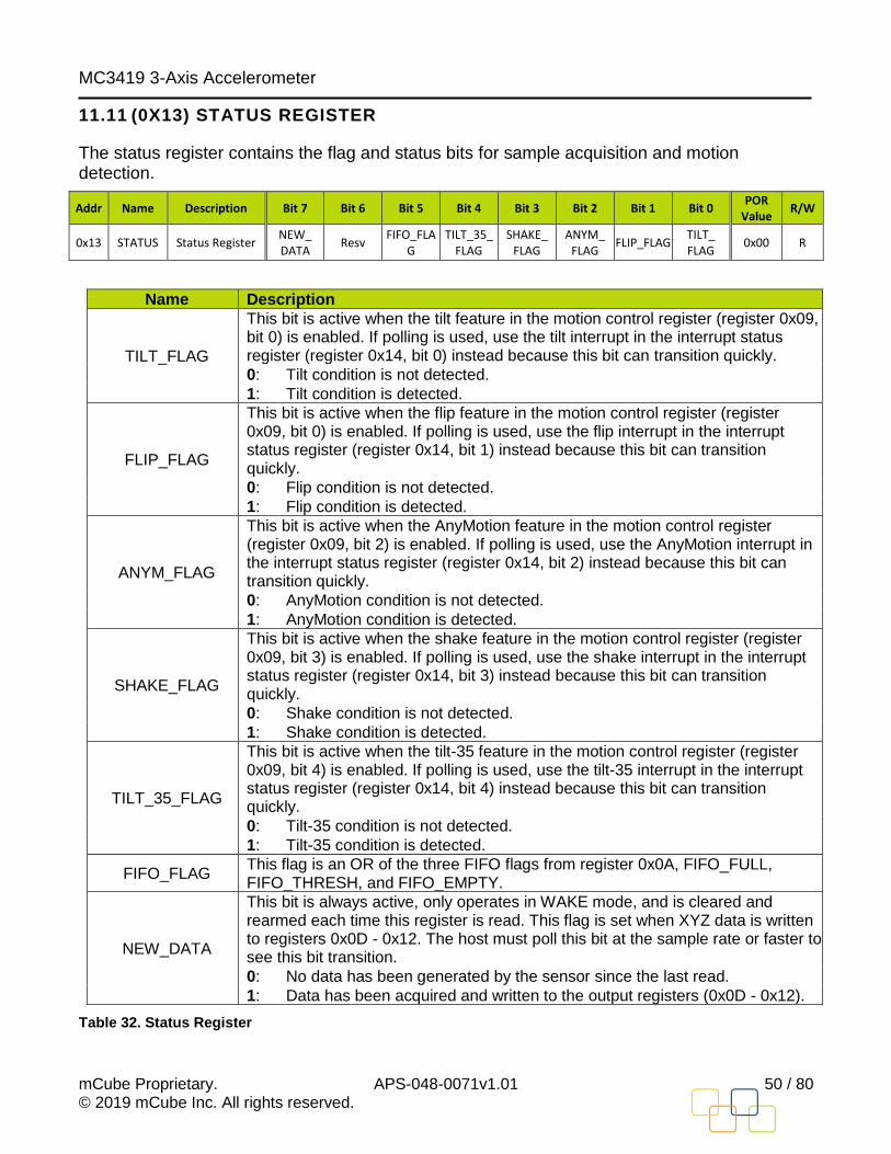
MC3419 3-Axis Accelerometer
mCube Proprietary. APS-048-0071v1.01 50 / 80 © 2019 mCube Inc. All rights reserved.
11.11 (0X13) STATUS REGISTER
The status register contains the flag and status bits for sample acquisition and motion detection.
Addr Name Description Bit 7 Bit 6 Bit 5 Bit 4 Bit 3 Bit 2 Bit 1 Bit 0 POR
Value R/W
0x13 STATUS Status Register NEW_ DATA
Resv FIFO_FLA
G TILT_35_
FLAG SHAKE_
FLAG ANYM_
FLAG FLIP_FLAG
TILT_ FLAG
0x00 R
Name Description
TILT_FLAG
This bit is active when the tilt feature in the motion control register (register 0x09, bit 0) is enabled. If polling is used, use the tilt interrupt in the interrupt status register (register 0x14, bit 0) instead because this bit can transition quickly.
0: Tilt condition is not detected.
1: Tilt condition is detected.
FLIP_FLAG
This bit is active when the flip feature in the motion control register (register 0x09, bit 0) is enabled. If polling is used, use the flip interrupt in the interrupt status register (register 0x14, bit 1) instead because this bit can transition quickly.
0: Flip condition is not detected.
1: Flip condition is detected.
ANYM_FLAG
This bit is active when the AnyMotion feature in the motion control register (register 0x09, bit 2) is enabled. If polling is used, use the AnyMotion interrupt in the interrupt status register (register 0x14, bit 2) instead because this bit can transition quickly.
0: AnyMotion condition is not detected.
1: AnyMotion condition is detected.
SHAKE_FLAG
This bit is active when the shake feature in the motion control register (register 0x09, bit 3) is enabled. If polling is used, use the shake interrupt in the interrupt status register (register 0x14, bit 3) instead because this bit can transition quickly.
0: Shake condition is not detected.
1: Shake condition is detected.
TILT_35_FLAG
This bit is active when the tilt-35 feature in the motion control register (register 0x09, bit 4) is enabled. If polling is used, use the tilt-35 interrupt in the interrupt status register (register 0x14, bit 4) instead because this bit can transition quickly.
0: Tilt-35 condition is not detected.
1: Tilt-35 condition is detected.
FIFO_FLAG This flag is an OR of the three FIFO flags from register 0x0A, FIFO_FULL, FIFO_THRESH, and FIFO_EMPTY.
NEW_DATA
This bit is always active, only operates in WAKE mode, and is cleared and rearmed each time this register is read. This flag is set when XYZ data is written to registers 0x0D - 0x12. The host must poll this bit at the sample rate or faster to see this bit transition.
0: No data has been generated by the sensor since the last read.
1: Data has been acquired and written to the output registers (0x0D - 0x12).
Table 32. Status Register
MC3419 3-Axis Accelerometer
mCube Proprietary. APS-048-0071v1.01 51 / 80 © 2019 mCube Inc. All rights reserved.
11.12 (0X14) INTERRUPT STATUS REGISTER
The interrupt status register reports the status of any pending interrupt sources. Each interrupt source must be enabled by the corresponding interrupt enable bit in register 0x06. All interrupts are cleared each time this register is written (default). Individual interrupts may be cleared using a bitmask if the INDIV_INTR_CLR bit is set in the communications control register, address 0x31.
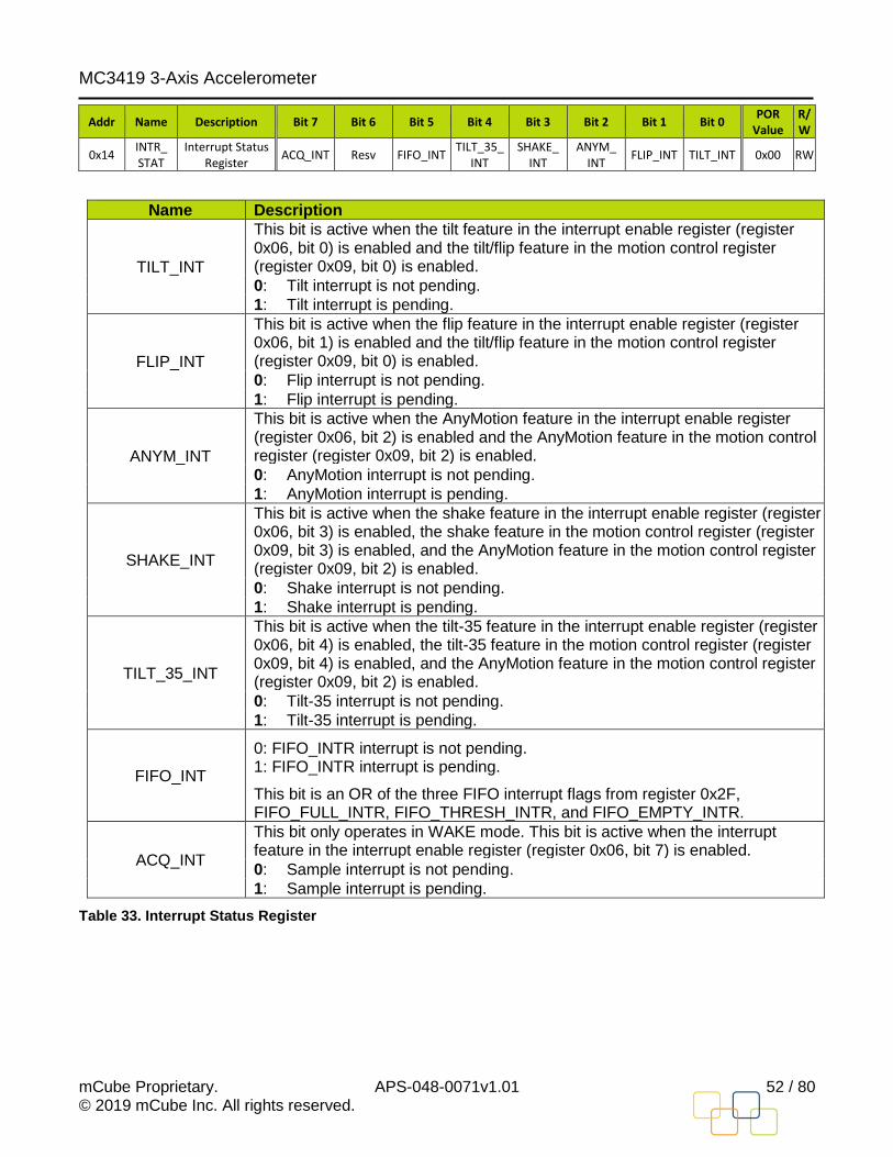
MC3419 3-Axis Accelerometer
mCube Proprietary. APS-048-0071v1.01 52 / 80 © 2019 mCube Inc. All rights reserved.
Addr Name Description Bit 7 Bit 6 Bit 5 Bit 4 Bit 3 Bit 2 Bit 1 Bit 0 POR
Value R/W
0x14 INTR_ STAT
Interrupt Status Register
ACQ_INT Resv FIFO_INT TILT_35_
INT SHAKE_
INT ANYM_
INT FLIP_INT TILT_INT 0x00 RW
Name Description
TILT_INT
This bit is active when the tilt feature in the interrupt enable register (register 0x06, bit 0) is enabled and the tilt/flip feature in the motion control register (register 0x09, bit 0) is enabled.
0: Tilt interrupt is not pending.
1: Tilt interrupt is pending.
FLIP_INT
This bit is active when the flip feature in the interrupt enable register (register 0x06, bit 1) is enabled and the tilt/flip feature in the motion control register (register 0x09, bit 0) is enabled.
0: Flip interrupt is not pending.
1: Flip interrupt is pending.
ANYM_INT
This bit is active when the AnyMotion feature in the interrupt enable register (register 0x06, bit 2) is enabled and the AnyMotion feature in the motion control register (register 0x09, bit 2) is enabled.
0: AnyMotion interrupt is not pending.
1: AnyMotion interrupt is pending.
SHAKE_INT
This bit is active when the shake feature in the interrupt enable register (register 0x06, bit 3) is enabled, the shake feature in the motion control register (register 0x09, bit 3) is enabled, and the AnyMotion feature in the motion control register (register 0x09, bit 2) is enabled.
0: Shake interrupt is not pending.
1: Shake interrupt is pending.
TILT_35_INT
This bit is active when the tilt-35 feature in the interrupt enable register (register 0x06, bit 4) is enabled, the tilt-35 feature in the motion control register (register 0x09, bit 4) is enabled, and the AnyMotion feature in the motion control register (register 0x09, bit 2) is enabled.
0: Tilt-35 interrupt is not pending.
1: Tilt-35 interrupt is pending.
FIFO_INT
0: FIFO_INTR interrupt is not pending. 1: FIFO_INTR interrupt is pending.
This bit is an OR of the three FIFO interrupt flags from register 0x2F, FIFO_FULL_INTR, FIFO_THRESH_INTR, and FIFO_EMPTY_INTR.
ACQ_INT
This bit only operates in WAKE mode. This bit is active when the interrupt feature in the interrupt enable register (register 0x06, bit 7) is enabled.
0: Sample interrupt is not pending.
1: Sample interrupt is pending.
Table 33. Interrupt Status Register
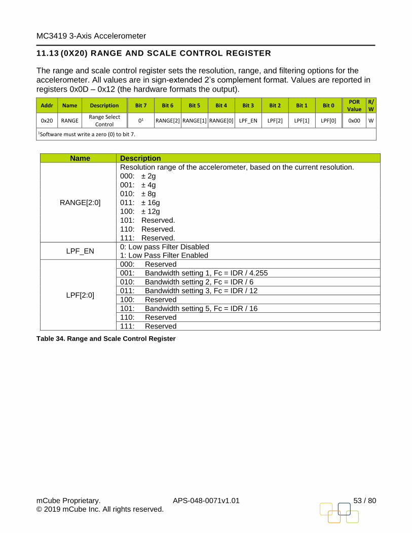
MC3419 3-Axis Accelerometer
mCube Proprietary. APS-048-0071v1.01 53 / 80 © 2019 mCube Inc. All rights reserved.
11.13 (0X20) RANGE AND SCALE CONTROL REGISTER
The range and scale control register sets the resolution, range, and filtering options for the accelerometer. All values are in sign-extended 2’s complement format. Values are reported in registers 0x0D – 0x12 (the hardware formats the output).
Addr Name Description Bit 7 Bit 6 Bit 5 Bit 4 Bit 3 Bit 2 Bit 1 Bit 0 POR
Value R/W
0x20 RANGE Range Select
Control 01 RANGE[2] RANGE[1] RANGE[0] LPF_EN LPF[2] LPF[1] LPF[0] 0x00 W
1Software must write a zero (0) to bit 7.
Name Description
RANGE[2:0]
Resolution range of the accelerometer, based on the current resolution.
000: ± 2g
001: ± 4g
010: ± 8g
011: ± 16g
100: ± 12g
101: Reserved.
110: Reserved.
111: Reserved.
LPF_EN 0: Low pass Filter Disabled 1: Low Pass Filter Enabled
LPF[2:0]
000: Reserved
001: Bandwidth setting 1, Fc = IDR / 4.255
010: Bandwidth setting 2, Fc = IDR / 6
011: Bandwidth setting 3, Fc = IDR / 12
100: Reserved
101: Bandwidth setting 5, Fc = IDR / 16
110: Reserved
111: Reserved
Table 34. Range and Scale Control Register

MC3419 3-Axis Accelerometer
mCube Proprietary. APS-048-0071v1.01 54 / 80 © 2019 mCube Inc. All rights reserved.
11.14 (0X21 – 0X22) X-AXIS DIGITAL OFFSET REGISTERS
The X-axis digital offset registers contains a signed 2’s complement 14-bit value used to offset the output of the X-axis filter. These registers are loaded from the OTP at device initialization and POR. If necessary, these values can be overwritten by software.
Register 0x22 bit 7 is the ninth bit of X-axis gain (XGAIN). See X-Axis Digital Gain Registers for more information about XGAIN.
NOTE: When modifying these registers with new gain or offset values, software should perform a read-modify-write type of access to ensure that unrelated bits do not get changed.
Addr Name Description Bit 7 Bit 6 Bit 5 Bit 4 Bit 3 Bit 2 Bit 1 Bit 0 POR
Value R/W
0x21 XOFFL X-Offset
LSB XOFF[7] XOFF[6] XOFF[5] XOFF[4] XOFF[3] XOFF[2] XOFF[1] XOFF[0] Per chip W
0x22 XOFFH X-Offset
MSB XGAIN[8] XOFF[14] XOFF[13] XOFF[12] XOFF[11] XOFF[10] XOFF[9] XOFF[8] Per chip W
Table 35. X-Axis Digital Offset Registers
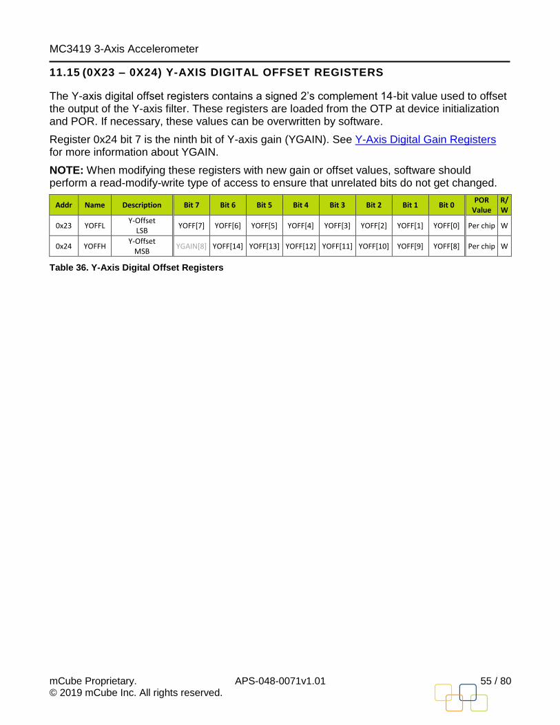
MC3419 3-Axis Accelerometer
mCube Proprietary. APS-048-0071v1.01 55 / 80 © 2019 mCube Inc. All rights reserved.
11.15 (0X23 – 0X24) Y-AXIS DIGITAL OFFSET REGISTERS
The Y-axis digital offset registers contains a signed 2’s complement 14-bit value used to offset the output of the Y-axis filter. These registers are loaded from the OTP at device initialization and POR. If necessary, these values can be overwritten by software.
Register 0x24 bit 7 is the ninth bit of Y-axis gain (YGAIN). See Y-Axis Digital Gain Registers for more information about YGAIN.
NOTE: When modifying these registers with new gain or offset values, software should perform a read-modify-write type of access to ensure that unrelated bits do not get changed.
Addr Name Description Bit 7 Bit 6 Bit 5 Bit 4 Bit 3 Bit 2 Bit 1 Bit 0 POR
Value R/W
0x23 YOFFL Y-Offset
LSB YOFF[7] YOFF[6] YOFF[5] YOFF[4] YOFF[3] YOFF[2] YOFF[1] YOFF[0] Per chip W
0x24 YOFFH Y-Offset
MSB YGAIN[8] YOFF[14] YOFF[13] YOFF[12] YOFF[11] YOFF[10] YOFF[9] YOFF[8] Per chip W
Table 36. Y-Axis Digital Offset Registers

MC3419 3-Axis Accelerometer
mCube Proprietary. APS-048-0071v1.01 56 / 80 © 2019 mCube Inc. All rights reserved.
11.16 (0X25 – 0X26) Z-AXIS DIGITAL OFFSET REGISTERS
The Z-axis digital offset registers contains a signed 2’s complement 14-bit value used to offset the output of the Z-axis filter. These registers are loaded from the OTP at device initialization and POR. If necessary, these values can be overwritten by software.
Register 0x26 bit 7 is the ninth bit of Z-axis gain (ZGAIN). See Z-Axis Digital Gain Registers for more information about ZGAIN.
NOTE: When modifying these registers with new gain or offset values, software should perform a read-modify-write type of access to ensure that unrelated bits do not get changed.
Addr Name Description Bit 7 Bit 6 Bit 5 Bit 4 Bit 3 Bit 2 Bit 1 Bit 0 POR
Value R/W
0x25 ZOFFL Z-Offset
LSB ZOFF[7] ZOFF[6] ZOFF[5] ZOFF[4] ZOFF[3] ZOFF[2] ZOFF[1] ZOFF[0] Per chip W
0x26 ZOFFH Z-Offset
MSB ZGAIN[8] ZOFF[14] ZOFF[13] ZOFF[12] ZOFF[11] ZOFF[10] ZOFF[9] ZOFF[8] Per chip W
Table 37. Z-Axis Digital Offset Registers

MC3419 3-Axis Accelerometer
mCube Proprietary. APS-048-0071v1.01 57 / 80 © 2019 mCube Inc. All rights reserved.
11.17 (0X22 & 0X27) X-AXIS DIGITAL GAIN REGISTERS
The X-axis digital gain registers contains an unsigned 9-bit value. These registers are loaded from the OTP at device initialization and POR. If necessary, these values can be overwritten by software.
Register 0x22 bit 7 is the ninth bit of XGAIN.
NOTE: When modifying these registers with new gain values, software should perform a read-modify-write type of access to ensure that unrelated bits do not get changed.
Addr Name Description Bit 7 Bit 6 Bit 5 Bit 4 Bit 3 Bit 2 Bit 1 Bit 0 POR
Value R/W
0x22 XOFFH X-Offset
MSB XGAIN[8] XOFF[14] XOFF[13] XOFF[12] XOFF[11] XOFF[10] XOFF[9] XOFF[8] Per chip W
0x27 XGAIN X Gain XGAIN[7] XGAIN[6] XGAIN[5] XGAIN[4] XGAIN[3] XGAIN[2] XGAIN[1] XGAIN[0] Per chip W
Table 38. X-Axis Digital Gain Registers
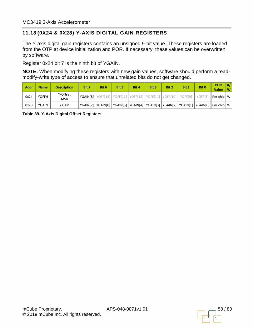
MC3419 3-Axis Accelerometer
mCube Proprietary. APS-048-0071v1.01 58 / 80 © 2019 mCube Inc. All rights reserved.
11.18 (0X24 & 0X28) Y-AXIS DIGITAL GAIN REGISTERS
The Y-axis digital gain registers contains an unsigned 9-bit value. These registers are loaded from the OTP at device initialization and POR. If necessary, these values can be overwritten by software.
Register 0x24 bit 7 is the ninth bit of YGAIN.
NOTE: When modifying these registers with new gain values, software should perform a read-modify-write type of access to ensure that unrelated bits do not get changed.
Addr Name Description Bit 7 Bit 6 Bit 5 Bit 4 Bit 3 Bit 2 Bit 1 Bit 0 POR
Value R/W
0x24 YOFFH Y-Offset
MSB YGAIN[8] YOFF[14] YOFF[13] YOFF[12] YOFF[11] YOFF[10] YOFF[9] YOFF[8] Per chip W
0x28 YGAIN Y Gain YGAIN[7] YGAIN[6] YGAIN[5] YGAIN[4] YGAIN[3] YGAIN[2] YGAIN[1] YGAIN[0] Per chip W
Table 39. Y-Axis Digital Offset Registers

MC3419 3-Axis Accelerometer
mCube Proprietary. APS-048-0071v1.01 59 / 80 © 2019 mCube Inc. All rights reserved.
11.19 (0X26 & 0X29) Z-AXIS DIGITAL GAIN REGISTERS
The Z-axis digital gain registers contains an unsigned 9-bit value. These registers are loaded from the OTP at device initialization and POR. If necessary, these values can be overwritten by software.
Register 0x26 bit 7 is the ninth bit of ZGAIN.
NOTE: When modifying these registers with new gain values, software should perform a read-modify-write type of access to ensure that unrelated bits do not get changed.
Addr Name Description Bit 7 Bit 6 Bit 5 Bit 4 Bit 3 Bit 2 Bit 1 Bit 0 POR
Value R/W
0x26 ZOFFH Z-Offset
MSB ZGAIN[8] ZOFF[14] ZOFF[13] ZOFF[12] ZOFF[11] ZOFF[10] ZOFF[9] ZOFF[8] Per chip W
0x29 ZGAIN Z Gain ZGAIN[7] ZGAIN[6] ZGAIN[5] ZGAIN[4] ZGAIN[3] ZGAIN[2] ZGAIN[1] ZGAIN[0] Per chip W
Table 40. Z-Axis Digital Offset Registers
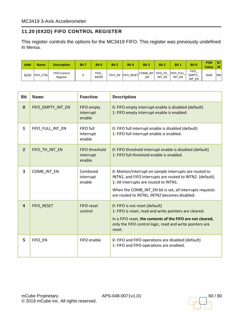
MC3419 3-Axis Accelerometer
mCube Proprietary. APS-048-0071v1.01 60 / 80 © 2019 mCube Inc. All rights reserved.
11.20 (0X2D) FIFO CONTROL REGISTER
This register controls the options for the MC3419 FIFO. This register was previously undefined in Mensa.
Addr Name Description Bit 7 Bit 6 Bit 5 Bit 4 Bit 3 Bit 2 Bit 1 Bit 0 POR
Value R/W
0x2D FIFO_CTRL FIFO Control
Register 0
FIFO_ MODE
FIFO_EN FIFO_RESET COMB_INT
_EN FIFO_TH_
INT_EN FIFO_FULL_
INT_EN
FIFO_ EMPTY_ INT_EN
0x00 RW
Bit Name Function Description
0 FIFO_EMPTY_INT_EN FIFO empty interrupt enable
0: FIFO empty interrupt enable is disabled (default) 1: FIFO empty interrupt enable is enabled.
1 FIFO_FULL_INT_EN FIFO full interrupt enable
0: FIFO full interrupt enable is disabled (default) 1: FIFO full interrupt enable is enabled.
2 FIFO_TH_INT_EN FIFO threshold interrupt enable.
0: FIFO threshold interrupt enable is disabled (default) 1: FIFO full threshold enable is enabled.
3 COMB_INT_EN Combined interrupt enable
0: Motion/interrupt on sample interrupts are routed to INTN1, and FIFO interrupts are routed to INTN2. (default). 1: All interrupts are routed to INTN1.
When the COMB_INT_EN bit is set, all interrupts requests are routed to INTN1, INTN2 becomes disabled.
4 FIFO_RESET FIFO reset control
0: FIFO is not reset (default) 1: FIFO is reset, read and write pointers are cleared.
In a FIFO reset, the contents of the FIFO are not cleared, only the FIFO control logic, read and write pointers are reset.
5 FIFO_EN FIFO enable 0: FIFO and FIFO operations are disabled (default) 1: FIFO and FIFO operations are enabled.
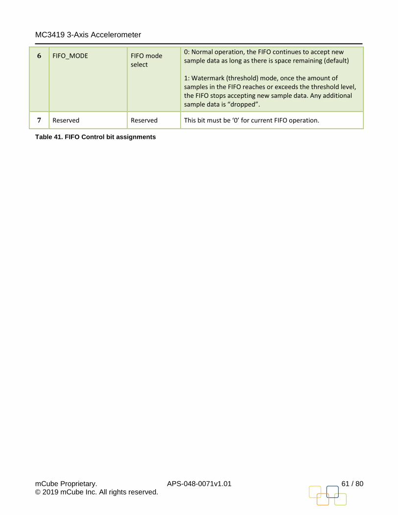
MC3419 3-Axis Accelerometer
mCube Proprietary. APS-048-0071v1.01 61 / 80 © 2019 mCube Inc. All rights reserved.
6 FIFO_MODE FIFO mode select
0: Normal operation, the FIFO continues to accept new sample data as long as there is space remaining (default) 1: Watermark (threshold) mode, once the amount of samples in the FIFO reaches or exceeds the threshold level, the FIFO stops accepting new sample data. Any additional sample data is “dropped”.
7 Reserved Reserved This bit must be ‘0’ for current FIFO operation.
Table 41. FIFO Control bit assignments
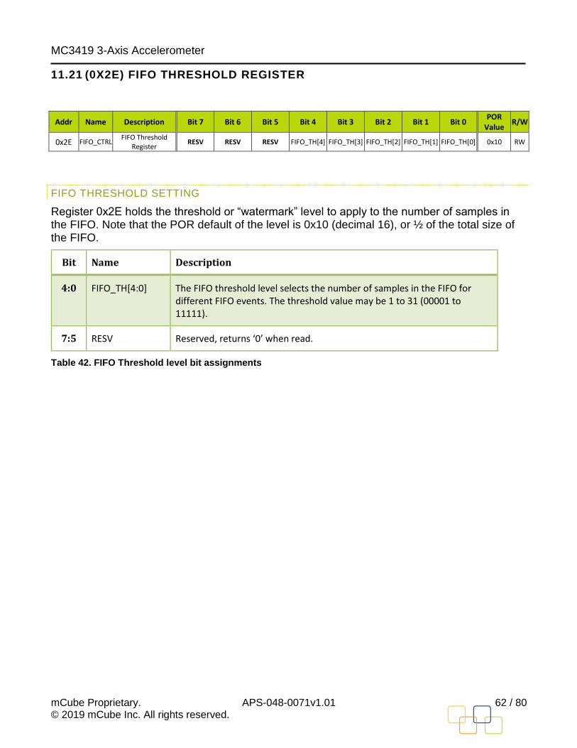
MC3419 3-Axis Accelerometer
mCube Proprietary. APS-048-0071v1.01 62 / 80 © 2019 mCube Inc. All rights reserved.
11.21 (0X2E) FIFO THRESHOLD REGISTER
Addr Name Description Bit 7 Bit 6 Bit 5 Bit 4 Bit 3 Bit 2 Bit 1 Bit 0 POR
Value R/W
0x2E FIFO_CTRL FIFO Threshold
Register RESV RESV RESV FIFO_TH[4] FIFO_TH[3] FIFO_TH[2] FIFO_TH[1] FIFO_TH[0] 0x10 RW
FIFO THRESHOLD SETTING
Register 0x2E holds the threshold or “watermark” level to apply to the number of samples in the FIFO. Note that the POR default of the level is 0x10 (decimal 16), or ½ of the total size of the FIFO.
Bit Name Description
4:0 FIFO_TH[4:0] The FIFO threshold level selects the number of samples in the FIFO for different FIFO events. The threshold value may be 1 to 31 (00001 to 11111).
7:5 RESV Reserved, returns ‘0’ when read.
Table 42. FIFO Threshold level bit assignments
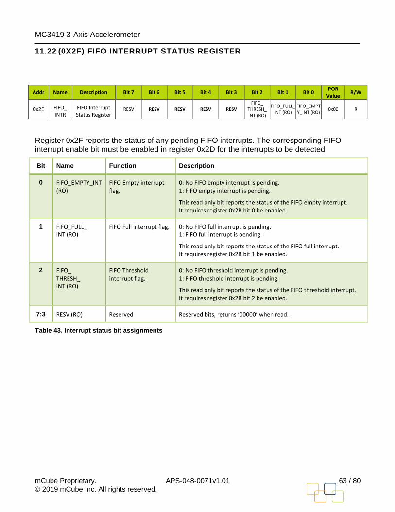
MC3419 3-Axis Accelerometer
mCube Proprietary. APS-048-0071v1.01 63 / 80 © 2019 mCube Inc. All rights reserved.
11.22 (0X2F) FIFO INTERRUPT STATUS REGISTER
Addr Name Description Bit 7 Bit 6 Bit 5 Bit 4 Bit 3 Bit 2 Bit 1 Bit 0 POR
Value R/W
0x2E FIFO_ INTR
FIFO Interrupt Status Register
RESV RESV RESV RESV RESV FIFO_
THRESH_ INT (RO)
FIFO_FULL_ INT (RO)
FIFO_EMPTY_INT (RO)
0x00 R
Register 0x2F reports the status of any pending FIFO interrupts. The corresponding FIFO interrupt enable bit must be enabled in register 0x2D for the interrupts to be detected.
Bit Name Function Description
0 FIFO_EMPTY_INT (RO)
FIFO Empty interrupt flag.
0: No FIFO empty interrupt is pending. 1: FIFO empty interrupt is pending.
This read only bit reports the status of the FIFO empty interrupt. It requires register 0x2B bit 0 be enabled.
1 FIFO_FULL_ INT (RO)
FIFO Full interrupt flag. 0: No FIFO full interrupt is pending. 1: FIFO full interrupt is pending.
This read only bit reports the status of the FIFO full interrupt. It requires register 0x2B bit 1 be enabled.
2 FIFO_ THRESH_ INT (RO)
FIFO Threshold interrupt flag.
0: No FIFO threshold interrupt is pending. 1: FIFO threshold interrupt is pending.
This read only bit reports the status of the FIFO threshold interrupt. It requires register 0x2B bit 2 be enabled.
7:3 RESV (RO) Reserved Reserved bits, returns ‘00000’ when read.
Table 43. Interrupt status bit assignments
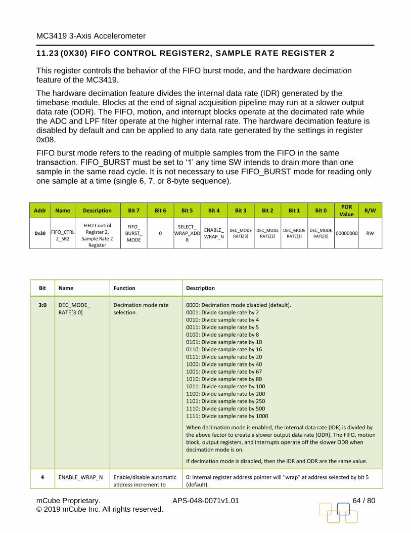
MC3419 3-Axis Accelerometer
mCube Proprietary. APS-048-0071v1.01 64 / 80 © 2019 mCube Inc. All rights reserved.
11.23 (0X30) FIFO CONTROL REGISTER2, SAMPLE RATE REGISTER 2
This register controls the behavior of the FIFO burst mode, and the hardware decimation feature of the MC3419.
The hardware decimation feature divides the internal data rate (IDR) generated by the timebase module. Blocks at the end of signal acquisition pipeline may run at a slower output data rate (ODR). The FIFO, motion, and interrupt blocks operate at the decimated rate while the ADC and LPF filter operate at the higher internal rate. The hardware decimation feature is disabled by default and can be applied to any data rate generated by the settings in register 0x08.
FIFO burst mode refers to the reading of multiple samples from the FIFO in the same transaction. FIFO_BURST must be set to ‘1’ any time SW intends to drain more than one sample in the same read cycle. It is not necessary to use FIFO_BURST mode for reading only one sample at a time (single 6, 7, or 8-byte sequence).
Addr Name Description Bit 7 Bit 6 Bit 5 Bit 4 Bit 3 Bit 2 Bit 1 Bit 0 POR
Value R/W
0x30 FIFO_CTRL2_SR2
FIFO Control Register 2,
Sample Rate 2 Register
FIFO_ BURST_ MODE
0 SELECT_
WRAP_ADDR
ENABLE_ WRAP_N
DEC_MODE RATE[3]
DEC_MODE RATE[2]
DEC_MODE RATE[1]
DEC_MODE RATE[0] 00000000 RW
Bit Name Function Description
3:0 DEC_MODE_ RATE[3:0]
Decimation mode rate selection.
0000: Decimation mode disabled (default). 0001: Divide sample rate by 2 0010: Divide sample rate by 4 0011: Divide sample rate by 5 0100: Divide sample rate by 8 0101: Divide sample rate by 10 0110: Divide sample rate by 16 0111: Divide sample rate by 20 1000: Divide sample rate by 40 1001: Divide sample rate by 67 1010: Divide sample rate by 80 1011: Divide sample rate by 100 1100: Divide sample rate by 200 1101: Divide sample rate by 250 1110: Divide sample rate by 500 1111: Divide sample rate by 1000
When decimation mode is enabled, the internal data rate (IDR) is divided by the above factor to create a slower output data rate (ODR). The FIFO, motion block, output registers, and interrupts operate off the slower ODR when decimation mode is on.
If decimation mode is disabled, then the IDR and ODR are the same value.
4 ENABLE_WRAP_N Enable/disable automatic address increment to
0: Internal register address pointer will “wrap” at address selected by bit 5 (default).
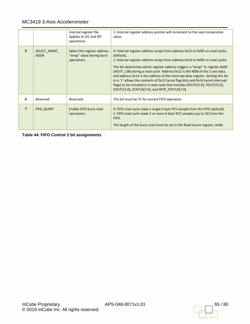
MC3419 3-Axis Accelerometer
mCube Proprietary. APS-048-0071v1.01 65 / 80 © 2019 mCube Inc. All rights reserved.
internal register file. Applies to I2C and SPI operations.
1: Internal register address pointer will increment to the next consecutive value.
5 SELECT_WRAP_ ADDR
Select the register address “wrap” value during burst operations.
0: Internal register address wraps from address 0x12 to 0x0D on read cycles. (default). 1: Internal register address wraps from address 0x14 to 0x0D on read cycles.
This bit determines which register address triggers a “wrap” to register 0x0D (XOUT_LSB) during a read cycle. Address 0x12 is the MSB of the Z-axis data, and address 0x14 is the address of the interrupt data register. Setting this bit to a ‘1’ allows the contents of 0x13 (accel flag bits) and 0x14 (accel interrupt flags) to be included in a read cycle that includes XOUT[15:0], YOUT[15:0], ZOUT[15:0], STATUS[7:0], and INTR_STATUS[7:0].
6 Reserved Reserved. This bit must be ‘0’ for correct FIFO operation.
7 FIFO_BURST Enable FIFO burst read operations.
0: FIFO read cycle reads a single 6 byte XYZ sample from the FIFO (default). 1: FIFO read cycle reads 2 or more 6-byte XYZ samples (up to 32) from the FIFO.
The length of the burst read must be set in the Read Count register, 0x4B.
Table 44. FIFO Control 2 bit assignments
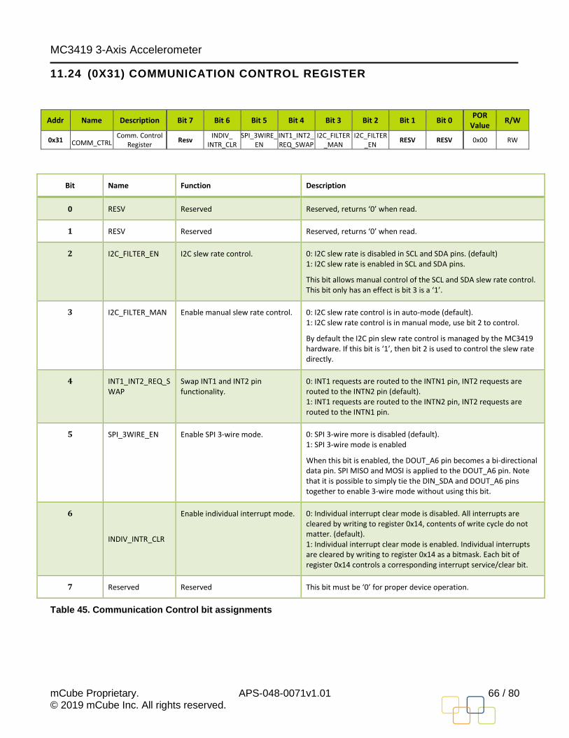
MC3419 3-Axis Accelerometer
mCube Proprietary. APS-048-0071v1.01 66 / 80 © 2019 mCube Inc. All rights reserved.
11.24 (0X31) COMMUNICATION CONTROL REGISTER
Addr Name Description Bit 7 Bit 6 Bit 5 Bit 4 Bit 3 Bit 2 Bit 1 Bit 0 POR
Value R/W
0x31 COMM_CTRL Comm. Control
Register Resv
INDIV_ INTR_CLR
SPI_3WIRE_ EN
INT1_INT2_REQ_SWAP
I2C_FILTER_MAN
I2C_FILTER_EN
RESV RESV 0x00 RW
Bit Name Function Description
0 RESV Reserved Reserved, returns ‘0’ when read.
1 RESV Reserved Reserved, returns ‘0’ when read.
2 I2C_FILTER_EN I2C slew rate control. 0: I2C slew rate is disabled in SCL and SDA pins. (default) 1: I2C slew rate is enabled in SCL and SDA pins.
This bit allows manual control of the SCL and SDA slew rate control. This bit only has an effect is bit 3 is a ‘1’.
3 I2C_FILTER_MAN Enable manual slew rate control. 0: I2C slew rate control is in auto-mode (default). 1: I2C slew rate control is in manual mode, use bit 2 to control.
By default the I2C pin slew rate control is managed by the MC3419 hardware. If this bit is ‘1’, then bit 2 is used to control the slew rate directly.
4 INT1_INT2_REQ_SWAP
Swap INT1 and INT2 pin functionality.
0: INT1 requests are routed to the INTN1 pin, INT2 requests are routed to the INTN2 pin (default). 1: INT1 requests are routed to the INTN2 pin, INT2 requests are routed to the INTN1 pin.
5 SPI_3WIRE_EN Enable SPI 3-wire mode. 0: SPI 3-wire more is disabled (default). 1: SPI 3-wire mode is enabled
When this bit is enabled, the DOUT_A6 pin becomes a bi-directional data pin. SPI MISO and MOSI is applied to the DOUT_A6 pin. Note that it is possible to simply tie the DIN_SDA and DOUT_A6 pins together to enable 3-wire mode without using this bit.
6
INDIV_INTR_CLR
Enable individual interrupt mode. 0: Individual interrupt clear mode is disabled. All interrupts are cleared by writing to register 0x14, contents of write cycle do not matter. (default). 1: Individual interrupt clear mode is enabled. Individual interrupts are cleared by writing to register 0x14 as a bitmask. Each bit of register 0x14 controls a corresponding interrupt service/clear bit.
7 Reserved Reserved This bit must be ‘0’ for proper device operation.
Table 45. Communication Control bit assignments
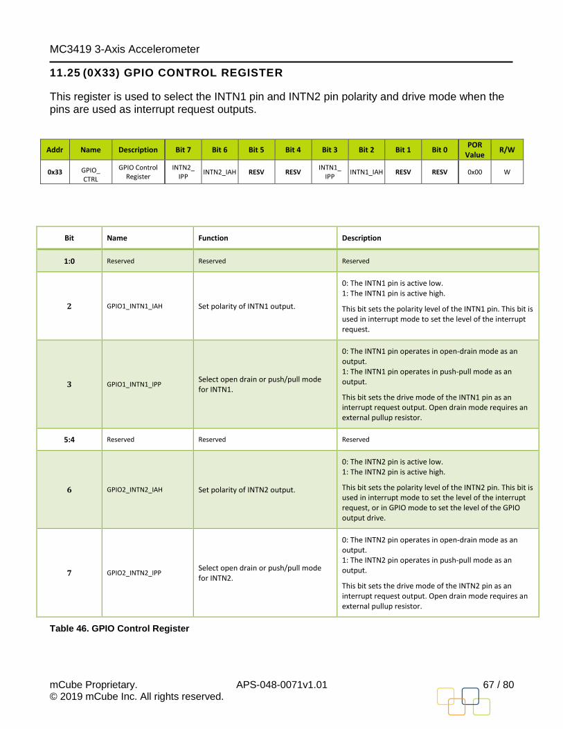
MC3419 3-Axis Accelerometer
mCube Proprietary. APS-048-0071v1.01 67 / 80 © 2019 mCube Inc. All rights reserved.
11.25 (0X33) GPIO CONTROL REGISTER
This register is used to select the INTN1 pin and INTN2 pin polarity and drive mode when the pins are used as interrupt request outputs.
Addr Name Description Bit 7 Bit 6 Bit 5 Bit 4 Bit 3 Bit 2 Bit 1 Bit 0 POR
Value R/W
0x33 GPIO_ CTRL
GPIO Control Register
INTN2_ IPP
INTN2_IAH RESV RESV INTN1_
IPP INTN1_IAH RESV RESV 0x00 W
Bit Name Function Description
1:0 Reserved Reserved Reserved
2 GPIO1_INTN1_IAH Set polarity of INTN1 output.
0: The INTN1 pin is active low. 1: The INTN1 pin is active high.
This bit sets the polarity level of the INTN1 pin. This bit is used in interrupt mode to set the level of the interrupt request.
3 GPIO1_INTN1_IPP Select open drain or push/pull mode for INTN1.
0: The INTN1 pin operates in open-drain mode as an output. 1: The INTN1 pin operates in push-pull mode as an output.
This bit sets the drive mode of the INTN1 pin as an interrupt request output. Open drain mode requires an external pullup resistor.
5:4 Reserved Reserved Reserved
6 GPIO2_INTN2_IAH Set polarity of INTN2 output.
0: The INTN2 pin is active low. 1: The INTN2 pin is active high.
This bit sets the polarity level of the INTN2 pin. This bit is used in interrupt mode to set the level of the interrupt request, or in GPIO mode to set the level of the GPIO output drive.
7 GPIO2_INTN2_IPP Select open drain or push/pull mode for INTN2.
0: The INTN2 pin operates in open-drain mode as an output. 1: The INTN2 pin operates in push-pull mode as an output.
This bit sets the drive mode of the INTN2 pin as an interrupt request output. Open drain mode requires an external pullup resistor.
Table 46. GPIO Control Register

MC3419 3-Axis Accelerometer
mCube Proprietary. APS-048-0071v1.01 68 / 80 © 2019 mCube Inc. All rights reserved.
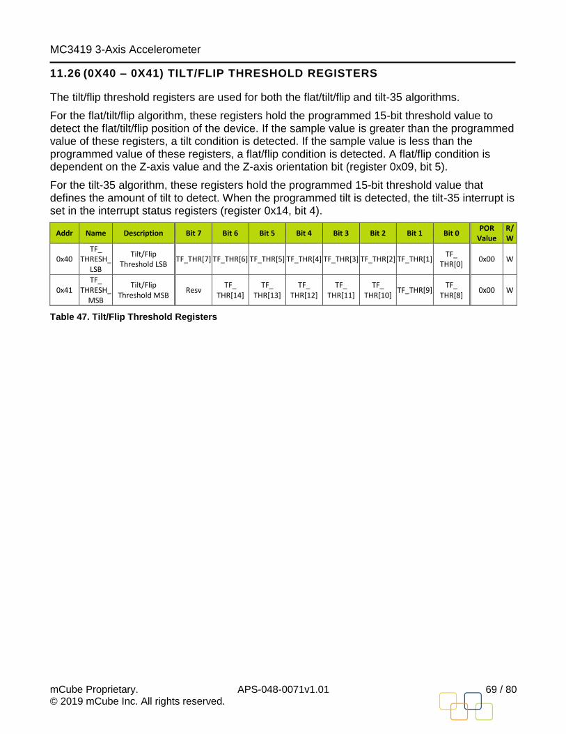
MC3419 3-Axis Accelerometer
mCube Proprietary. APS-048-0071v1.01 69 / 80 © 2019 mCube Inc. All rights reserved.
11.26 (0X40 – 0X41) TILT/FLIP THRESHOLD REGISTERS
The tilt/flip threshold registers are used for both the flat/tilt/flip and tilt-35 algorithms.
For the flat/tilt/flip algorithm, these registers hold the programmed 15-bit threshold value to detect the flat/tilt/flip position of the device. If the sample value is greater than the programmed value of these registers, a tilt condition is detected. If the sample value is less than the programmed value of these registers, a flat/flip condition is detected. A flat/flip condition is dependent on the Z-axis value and the Z-axis orientation bit (register 0x09, bit 5).
For the tilt-35 algorithm, these registers hold the programmed 15-bit threshold value that defines the amount of tilt to detect. When the programmed tilt is detected, the tilt-35 interrupt is set in the interrupt status registers (register 0x14, bit 4).
Addr Name Description Bit 7 Bit 6 Bit 5 Bit 4 Bit 3 Bit 2 Bit 1 Bit 0 POR
Value R/W
0x40 TF_
THRESH_LSB
Tilt/Flip Threshold LSB
TF_THR[7] TF_THR[6] TF_THR[5] TF_THR[4] TF_THR[3] TF_THR[2] TF_THR[1] TF_
THR[0] 0x00 W
0x41 TF_
THRESH_MSB
Tilt/Flip Threshold MSB
Resv TF_
THR[14] TF_
THR[13] TF_
THR[12] TF_
THR[11] TF_
THR[10] TF_THR[9]
TF_ THR[8]
0x00 W
Table 47. Tilt/Flip Threshold Registers
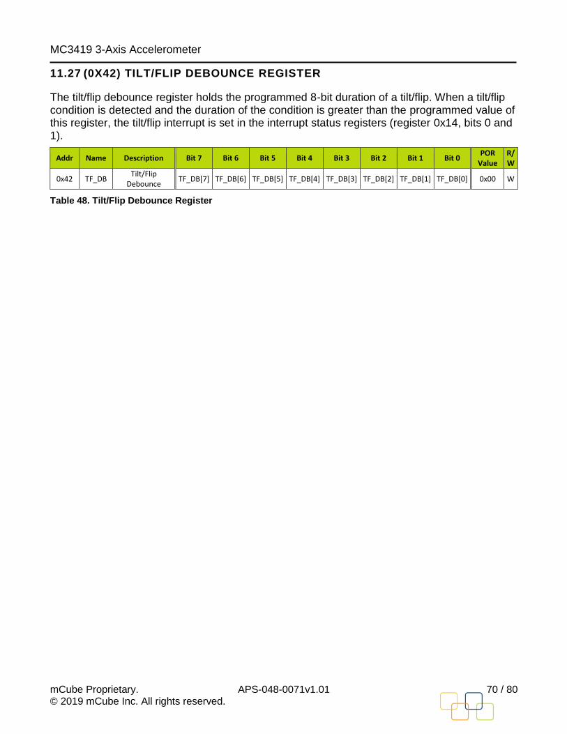
MC3419 3-Axis Accelerometer
mCube Proprietary. APS-048-0071v1.01 70 / 80 © 2019 mCube Inc. All rights reserved.
11.27 (0X42) TILT/FLIP DEBOUNCE REGISTER
The tilt/flip debounce register holds the programmed 8-bit duration of a tilt/flip. When a tilt/flip condition is detected and the duration of the condition is greater than the programmed value of this register, the tilt/flip interrupt is set in the interrupt status registers (register 0x14, bits 0 and 1).
Addr Name Description Bit 7 Bit 6 Bit 5 Bit 4 Bit 3 Bit 2 Bit 1 Bit 0 POR
Value R/W
0x42 TF_DB Tilt/Flip
Debounce TF_DB[7] TF_DB[6] TF_DB[5] TF_DB[4] TF_DB[3] TF_DB[2] TF_DB[1] TF_DB[0] 0x00 W
Table 48. Tilt/Flip Debounce Register
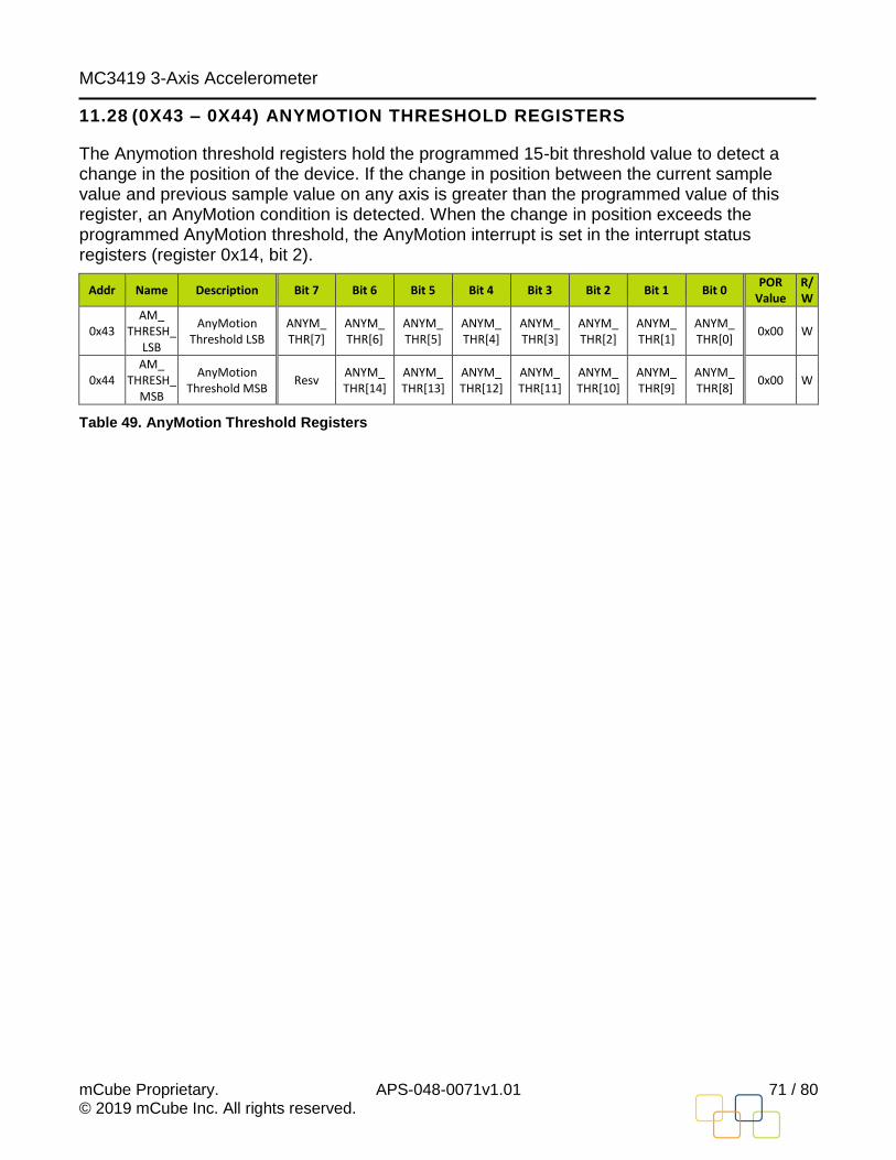
MC3419 3-Axis Accelerometer
mCube Proprietary. APS-048-0071v1.01 71 / 80 © 2019 mCube Inc. All rights reserved.
11.28 (0X43 – 0X44) ANYMOTION THRESHOLD REGISTERS
The Anymotion threshold registers hold the programmed 15-bit threshold value to detect a change in the position of the device. If the change in position between the current sample value and previous sample value on any axis is greater than the programmed value of this register, an AnyMotion condition is detected. When the change in position exceeds the programmed AnyMotion threshold, the AnyMotion interrupt is set in the interrupt status registers (register 0x14, bit 2).
Addr Name Description Bit 7 Bit 6 Bit 5 Bit 4 Bit 3 Bit 2 Bit 1 Bit 0 POR
Value R/W
0x43 AM_
THRESH_LSB
AnyMotion Threshold LSB
ANYM_ THR[7]
ANYM_ THR[6]
ANYM_ THR[5]
ANYM_ THR[4]
ANYM_ THR[3]
ANYM_ THR[2]
ANYM_ THR[1]
ANYM_ THR[0]
0x00 W
0x44 AM_
THRESH_MSB
AnyMotion Threshold MSB
Resv ANYM_ THR[14]
ANYM_ THR[13]
ANYM_ THR[12]
ANYM_ THR[11]
ANYM_ THR[10]
ANYM_ THR[9]
ANYM_ THR[8]
0x00 W
Table 49. AnyMotion Threshold Registers
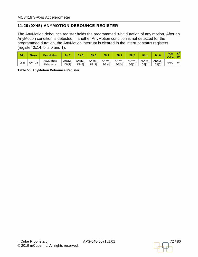
MC3419 3-Axis Accelerometer
mCube Proprietary. APS-048-0071v1.01 72 / 80 © 2019 mCube Inc. All rights reserved.
11.29 (0X45) ANYMOTION DEBOUNCE REGISTER
The AnyMotion debounce register holds the programmed 8-bit duration of any motion. After an AnyMotion condition is detected, if another AnyMotion condition is not detected for the programmed duration, the AnyMotion interrupt is cleared in the interrupt status registers (register 0x14, bits 0 and 1).
Addr Name Description Bit 7 Bit 6 Bit 5 Bit 4 Bit 3 Bit 2 Bit 1 Bit 0 POR
Value R/W
0x45 AM_DB AnyMotion Debounce
ANYM_ DB[7]
ANYM_ DB[6]
ANYM_ DB[5]
ANYM_ DB[4]
ANYM_ DB[3]
ANYM_ DB[2]
ANYM_ DB[1]
ANYM_ DB[0]
0x00 W
Table 50. AnyMotion Debounce Register
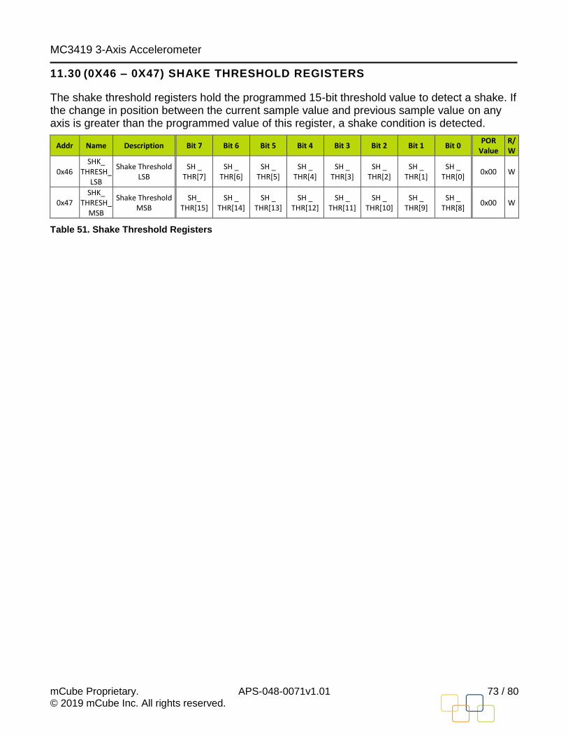
MC3419 3-Axis Accelerometer
mCube Proprietary. APS-048-0071v1.01 73 / 80 © 2019 mCube Inc. All rights reserved.
11.30 (0X46 – 0X47) SHAKE THRESHOLD REGISTERS
The shake threshold registers hold the programmed 15-bit threshold value to detect a shake. If the change in position between the current sample value and previous sample value on any axis is greater than the programmed value of this register, a shake condition is detected.
Addr Name Description Bit 7 Bit 6 Bit 5 Bit 4 Bit 3 Bit 2 Bit 1 Bit 0 POR
Value R/W
0x46 SHK_
THRESH_LSB
Shake Threshold LSB
SH _ THR[7]
SH _ THR[6]
SH _ THR[5]
SH _ THR[4]
SH _ THR[3]
SH _ THR[2]
SH _ THR[1]
SH _ THR[0]
0x00 W
0x47 SHK_
THRESH_MSB
Shake Threshold MSB
SH_ THR[15]
SH _ THR[14]
SH _ THR[13]
SH _ THR[12]
SH _ THR[11]
SH _ THR[10]
SH _ THR[9]
SH _ THR[8]
0x00 W
Table 51. Shake Threshold Registers
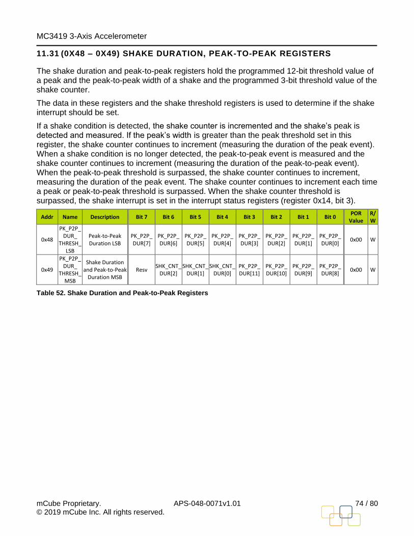
MC3419 3-Axis Accelerometer
mCube Proprietary. APS-048-0071v1.01 74 / 80 © 2019 mCube Inc. All rights reserved.
11.31 (0X48 – 0X49) SHAKE DURATION, PEAK-TO-PEAK REGISTERS
The shake duration and peak-to-peak registers hold the programmed 12-bit threshold value of a peak and the peak-to-peak width of a shake and the programmed 3-bit threshold value of the shake counter.
The data in these registers and the shake threshold registers is used to determine if the shake interrupt should be set.
If a shake condition is detected, the shake counter is incremented and the shake’s peak is detected and measured. If the peak’s width is greater than the peak threshold set in this register, the shake counter continues to increment (measuring the duration of the peak event). When a shake condition is no longer detected, the peak-to-peak event is measured and the shake counter continues to increment (measuring the duration of the peak-to-peak event). When the peak-to-peak threshold is surpassed, the shake counter continues to increment, measuring the duration of the peak event. The shake counter continues to increment each time a peak or peak-to-peak threshold is surpassed. When the shake counter threshold is surpassed, the shake interrupt is set in the interrupt status registers (register 0x14, bit 3).
Addr Name Description Bit 7 Bit 6 Bit 5 Bit 4 Bit 3 Bit 2 Bit 1 Bit 0 POR
Value R/W
0x48
PK_P2P_DUR_
THRESH_LSB
Peak-to-Peak Duration LSB
PK_P2P_ DUR[7]
PK_P2P_ DUR[6]
PK_P2P_ DUR[5]
PK_P2P_ DUR[4]
PK_P2P_ DUR[3]
PK_P2P_ DUR[2]
PK_P2P_ DUR[1]
PK_P2P_ DUR[0]
0x00 W
0x49
PK_P2P_DUR_
THRESH_MSB
Shake Duration and Peak-to-Peak
Duration MSB Resv
SHK_CNT_DUR[2]
SHK_CNT_DUR[1]
SHK_CNT_DUR[0]
PK_P2P_ DUR[11]
PK_P2P_ DUR[10]
PK_P2P_ DUR[9]
PK_P2P_ DUR[8]
0x00 W
Table 52. Shake Duration and Peak-to-Peak Registers
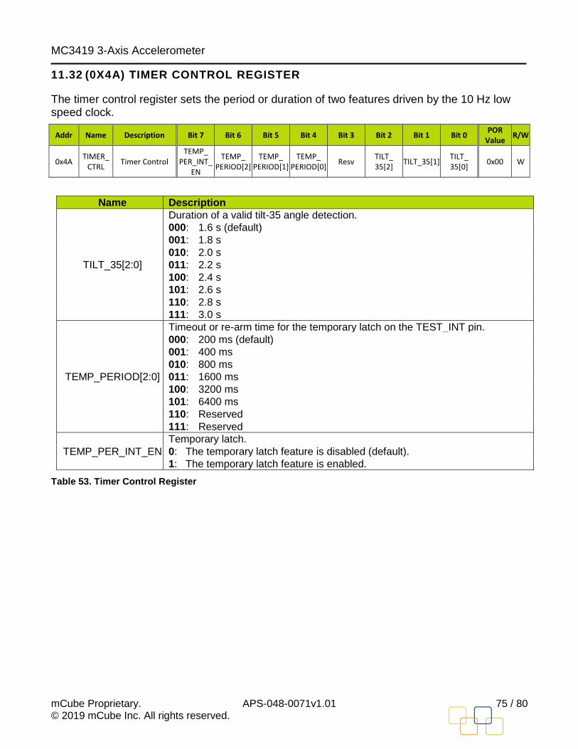
MC3419 3-Axis Accelerometer
mCube Proprietary. APS-048-0071v1.01 75 / 80 © 2019 mCube Inc. All rights reserved.
11.32 (0X4A) TIMER CONTROL REGISTER
The timer control register sets the period or duration of two features driven by the 10 Hz low speed clock.
Addr Name Description Bit 7 Bit 6 Bit 5 Bit 4 Bit 3 Bit 2 Bit 1 Bit 0 POR
Value R/W
0x4A TIMER_
CTRL Timer Control
TEMP_ PER_INT_
EN
TEMP_ PERIOD[2]
TEMP_ PERIOD[1]
TEMP_ PERIOD[0]
Resv TILT_ 35[2]
TILT_35[1] TILT_ 35[0]
0x00 W
Name Description
TILT_35[2:0]
Duration of a valid tilt-35 angle detection.
000: 1.6 s (default)
001: 1.8 s
010: 2.0 s
011: 2.2 s
100: 2.4 s
101: 2.6 s
110: 2.8 s
111: 3.0 s
TEMP_PERIOD[2:0]
Timeout or re-arm time for the temporary latch on the TEST_INT pin.
000: 200 ms (default)
001: 400 ms
010: 800 ms
011: 1600 ms
100: 3200 ms
101: 6400 ms
110: Reserved
111: Reserved
TEMP_PER_INT_EN
Temporary latch.
0: The temporary latch feature is disabled (default).
1: The temporary latch feature is enabled.
Table 53. Timer Control Register
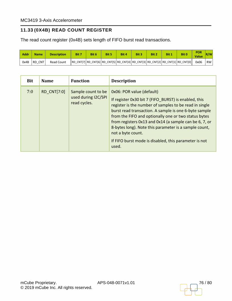
MC3419 3-Axis Accelerometer
mCube Proprietary. APS-048-0071v1.01 76 / 80 © 2019 mCube Inc. All rights reserved.
11.33 (0X4B) READ COUNT REGISTER
The read count register (0x4B) sets length of FIFO burst read transactions.
Addr Name Description Bit 7 Bit 6 Bit 5 Bit 4 Bit 3 Bit 2 Bit 1 Bit 0 POR
Value R/W
0x4B RD_CNT Read Count RD_CNT[7] RD_CNT[6] RD_CNT[5] RD_CNT[4] RD_CNT[3] RD_CNT[2] RD_CNT[1] RD_CNT[0] 0x06 RW
Bit Name Function Description
7:0 RD_CNT[7:0] Sample count to be used during I2C/SPI read cycles.
0x06: POR value (default)
If register 0x30 bit 7 (FIFO_BURST) is enabled, this register is the number of samples to be read in single burst read transaction. A sample is one 6-byte sample from the FIFO and optionally one or two status bytes from registers 0x13 and 0x14 (a sample can be 6, 7, or 8-bytes long). Note this parameter is a sample count, not a byte count.
If FIFO burst mode is disabled, this parameter is not used.
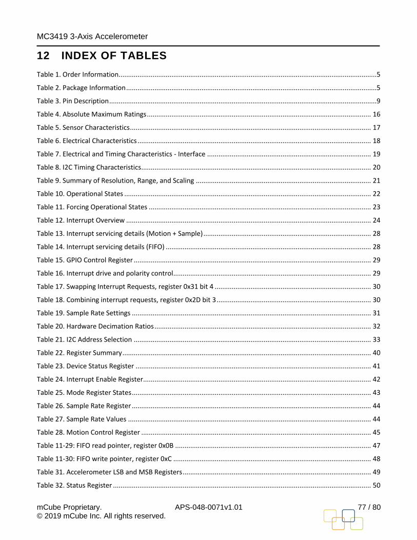
MC3419 3-Axis Accelerometer
mCube Proprietary. APS-048-0071v1.01 77 / 80 © 2019 mCube Inc. All rights reserved.
12 INDEX OF TABLES
Table 1. Order Information.........................................................................................................................................5
Table 2. Package Information .....................................................................................................................................5
Table 3. Pin Description ..............................................................................................................................................9
Table 4. Absolute Maximum Ratings ....................................................................................................................... 16
Table 5. Sensor Characteristics ................................................................................................................................ 17
Table 6. Electrical Characteristics ............................................................................................................................ 18
Table 7. Electrical and Timing Characteristics - Interface ....................................................................................... 19
Table 8. I2C Timing Characteristics .......................................................................................................................... 20
Table 9. Summary of Resolution, Range, and Scaling ............................................................................................. 21
Table 10. Operational States ................................................................................................................................... 22
Table 11. Forcing Operational States ...................................................................................................................... 23
Table 12. Interrupt Overview .................................................................................................................................. 24
Table 13. Interrupt servicing details (Motion + Sample) ......................................................................................... 28
Table 14. Interrupt servicing details (FIFO) ............................................................................................................. 28
Table 15. GPIO Control Register .............................................................................................................................. 29
Table 16. Interrupt drive and polarity control ......................................................................................................... 29
Table 17. Swapping Interrupt Requests, register 0x31 bit 4 ................................................................................... 30
Table 18. Combining interrupt requests, register 0x2D bit 3 .................................................................................. 30
Table 19. Sample Rate Settings ............................................................................................................................... 31
Table 20. Hardware Decimation Ratios ................................................................................................................... 32
Table 21. I2C Address Selection .............................................................................................................................. 33
Table 22. Register Summary .................................................................................................................................... 40
Table 23. Device Status Register ............................................................................................................................. 41
Table 24. Interrupt Enable Register ......................................................................................................................... 42
Table 25. Mode Register States ............................................................................................................................... 43
Table 26. Sample Rate Register ............................................................................................................................... 44
Table 27. Sample Rate Values ................................................................................................................................. 44
Table 28. Motion Control Register .......................................................................................................................... 45
Table 11-29: FIFO read pointer, register 0x0B ........................................................................................................ 47
Table 11-30: FIFO write pointer, register 0xC ......................................................................................................... 48
Table 31. Accelerometer LSB and MSB Registers .................................................................................................... 49
Table 32. Status Register ......................................................................................................................................... 50
MC3419 3-Axis Accelerometer
mCube Proprietary. APS-048-0071v1.01 78 / 80 © 2019 mCube Inc. All rights reserved.
Table 33. Interrupt Status Register ......................................................................................................................... 52
Table 34. Range and Scale Control Register ............................................................................................................ 53
Table 35. X-Axis Digital Offset Registers .................................................................................................................. 54
Table 36. Y-Axis Digital Offset Registers .................................................................................................................. 55
Table 37. Z-Axis Digital Offset Registers .................................................................................................................. 56
Table 38. X-Axis Digital Gain Registers .................................................................................................................... 57
Table 39. Y-Axis Digital Offset Registers .................................................................................................................. 58
Table 40. Z-Axis Digital Offset Registers .................................................................................................................. 59
Table 41. FIFO Control bit assignments ................................................................................................................... 61
Table 42. FIFO Threshold level bit assignments ...................................................................................................... 62
Table 43. Interrupt status bit assignments .............................................................................................................. 63
Table 44. FIFO Control 2 bit assignments ................................................................................................................ 65
Table 45. Communication Control bit assignments ................................................................................................ 66
Table 46. GPIO Control Register .............................................................................................................................. 67
Table 47. Tilt/Flip Threshold Registers .................................................................................................................... 69
Table 48. Tilt/Flip Debounce Register ..................................................................................................................... 70
Table 49. AnyMotion Threshold Registers .............................................................................................................. 71
Table 50. AnyMotion Debounce Register ................................................................................................................ 72
Table 51. Shake Threshold Registers ....................................................................................................................... 73
Table 52. Shake Duration and Peak-to-Peak Registers ........................................................................................... 74
Table 53. Timer Control Register ............................................................................................................................. 75

MC3419 3-Axis Accelerometer
mCube Proprietary. APS-048-0071v1.01 79 / 80 © 2019 mCube Inc. All rights reserved.
13 REVISION HISTORY
Date Revision Description
2019-05 APS-048-0071v1.0 Initial release
2019-06 APS-048-0071v1.01 Fixed a few typos

MC3419 3-Axis Accelerometer
mCube Proprietary. APS-048-0071v1.01 80 / 80 © 2019 mCube Inc. All rights reserved.
14 LEGAL
1. M-CUBE reserves the right to make corrections, modifications, enhancements, improvements and other changes to its
products and to this document at any time and discontinue any product without notice. The information contained in this
document has been carefully checked and is believed to be accurate. However, M-CUBE shall assume no responsibilities for
inaccuracies and make no commitment to update or to keep current the information contained in this document.
2. M-CUBE products are designed only for commercial and normal industrial applications and are not suitable for other
purposes, such as: medical life support equipment; nuclear facilities; critical care equipment; military / aerospace;
automotive; security or any other applications, the failure of which could lead to death, personal injury or environmental or
property damage. Use of the products in unsuitable applications are at the customer’s own risk and expense.
3. M-CUBE shall assume no liability for incidental, consequential or special damages or injury that may result from
misapplication or improper use of operation of the product.
4. No license, express or implied, by estoppel or otherwise, to any intellectual property rights of M-CUBE or any third
party is granted under this document.
5. M-CUBE makes no warranty or representation of non-infringement of intellectual property rights of any third party with
respect to the products. M-CUBE specifically excludes any liability to the customers or any third party regarding
infringement of any intellectual property rights, including the patent, copyright, trademark or trade secret rights of any third
party, relating to any combination, machine, or process in which the M-CUBE products are used.
6. Examples of use described herein are provided solely to guide use of M-CUBE products and merely indicate targeted
characteristics, performance and applications of products. M-CUBE shall assume no responsibility for any intellectual
property claims or other problems that may result from applications based on the examples described herein
7. Information described in this document including parameters, application circuits and its constants and calculation
formulas, programs and control procedures are provided for the purpose of explaining typical operation and usage. “Typical”
parameters that may be provided in M-CUBE data sheets and/or specifications can and do vary in different applications and
actual performance may vary over time. All operating parameters including “Typicals,” must be validated for each customer
application by customer’s technical experts. In no event shall the information described be regarded as a guarantee of
conditions or characteristics of the products. Therefore, the customer should evaluate the design sufficiently as whole system
under the consideration of various external or environmental conditions and determine their application at the customer’s
own risk. M-CUBE shall assume no responsibility or liability for claims, damages, costs and expenses caused by the
customer or any third party, owing to the use of the above information.
is a trademark of M-CUBE, Inc.
M-CUBE and the M-CUBE logo are trademarks of M-CUBE, Inc.,
All other product or service names are the property of their respective owners.
© M-CUBE, Inc. 2019. All rights reserved.


![Guidelines for PCB Design and Assembly with mCube Sensors · PCB Design, Device Handling and Assembly Guidelines – AN-001 mCube Proprietary and Confidential. [APS-045-0006R11] 2](https://static.fdocuments.net/doc/165x107/5e77e55782424348906df652/guidelines-for-pcb-design-and-assembly-with-mcube-sensors-pcb-design-device-handling.jpg)