GE Fanuc Automation - Qualitrol · 2018-11-27 · Introduction GFK-0074 l-l CHAPTER 1 INTRODUCTION...
214
GE Fanuc Automation Programmable Control Products Genius’” I/O PCIM User’s Manual
Transcript of GE Fanuc Automation - Qualitrol · 2018-11-27 · Introduction GFK-0074 l-l CHAPTER 1 INTRODUCTION...

GE Fanuc Automation
Programmable Control Products
Genius’” I/OPCIM
User’s Manual
GFL-00 1
Warnings, Cautions, and Notesas Used in this Publication
1 Warn ing 1
Warning notices are used in this publication to emphasize that hazardous voltages, currents,temperatures, or other conditions that could cause personal injury exist in this equipment or maybe associated with i ts use.
In situations where inattention could cause either personal injury or damage to equipment, aWarning notice is used.
Caution notices are used where equipment might be damaged if care is not taken.
NoteNotes merely call attention to information that is especially significant to understanding andoperat ing the equipment .
This document is based on information available at the time of its publication, While effortshave been made to be accurate, the information contained herein does not purport to cover alldetails or variations in hardware or software, nor to provide for every possible contingency inconnection with installation, operation, or maintenance. Features may be described hereinwhich are not present in all hardware and software systems. GE Fanuc Automation assumes noobligat ion of notice to holders of this document with respect to changes subsequently made.
GE Fanuc Automation makes no representation or warranty, expressed, implied, or statutorywith respect to, and assumes no responsibility for the accuracy, completeness, sufficiency, orusefulness of the information contained herein No warranties of merchantability or fitness forpurpose shal l apply.
@Copyright 1988 GE Fanuc Automation North America, Inc.
Al l Rights Reserved .
PCIM User’s Manual .*.III
GFK-0074
PREFACE
The intent of this manual is to supply the user with enough information to establish theGENIUS I/O IBM PC interface Module (PCIM) as an entry point into the GENIUS I/OSystem. The PCIM is designed to be integrated into a user-developed IBM PCmicroprocessor-based system. It provides a low cost ‘tap’ on the GENIUS I/O bus,allowing a host system to monitor and control remote I/O utilizing the extensivediagnostics, high reliability and noise immunity of GE Fanuc’s GENIUS l/O System.
Intended Audience
This manual is intended for design engineers and systems or applications programmerswho are already familiar with Basic or C programming in the IBM personal computerenvironment. Readers are further assumed to be familiar with the GENIUS I/O System.
How to use this Manual
This manual provides a description of the GE Fanuc GENIUS I/O IBM PC Interface Module(PCIM), and procedures for its setup, programming, operation, and troubleshooting from auser’s point of view. The manual should be regarded as a self-teaching tutorial if you areunfamiliar with the PCIM. The more experienced user will access it as a reference.
DO NOT ATTEMPT INSTALLATION, OPERATION, OR PROGRAMMING OF THE PCIMUNTIL YOU HAVE READ THE USER’S MANUAL FRONT TO BACK. Pay particularattention to the WARNINGS and CAUTIONS interspersed throughout the text, asELECTRICAL HAZARDS exist which could cause PERSONAL INJURY or DEATH, ordamage to the equipment.
i v PCIM User’s Manual
GFK-0074
Structure of this Manual
This manual contains 6 chapters and 7 appendices:
Chapter 1 - Introduction
Chapter 2 - Theory of Operation ’
Chapter 3 - Getting Started
Chapter 4 - Using PCIM - Software Drivers
Chapter 5 - Communications
Chapter 6 - Troubleshooting
Appendix A - Example Application
Appendix B - Glossary
Appendix C - Connector Signal Descriptions
Appendix D - Specifications
Appendix E - Part Numbers
Appendix F - Function Codes
Related Publications
The following documents in association with this manual comprise the PCIM User’sPackage:
a GENIUS IO Bus Datagram Reference Manual - GFK-0090
? GENIUS IO User’s Manual - GEK-90486
Contents V
GFK-0074
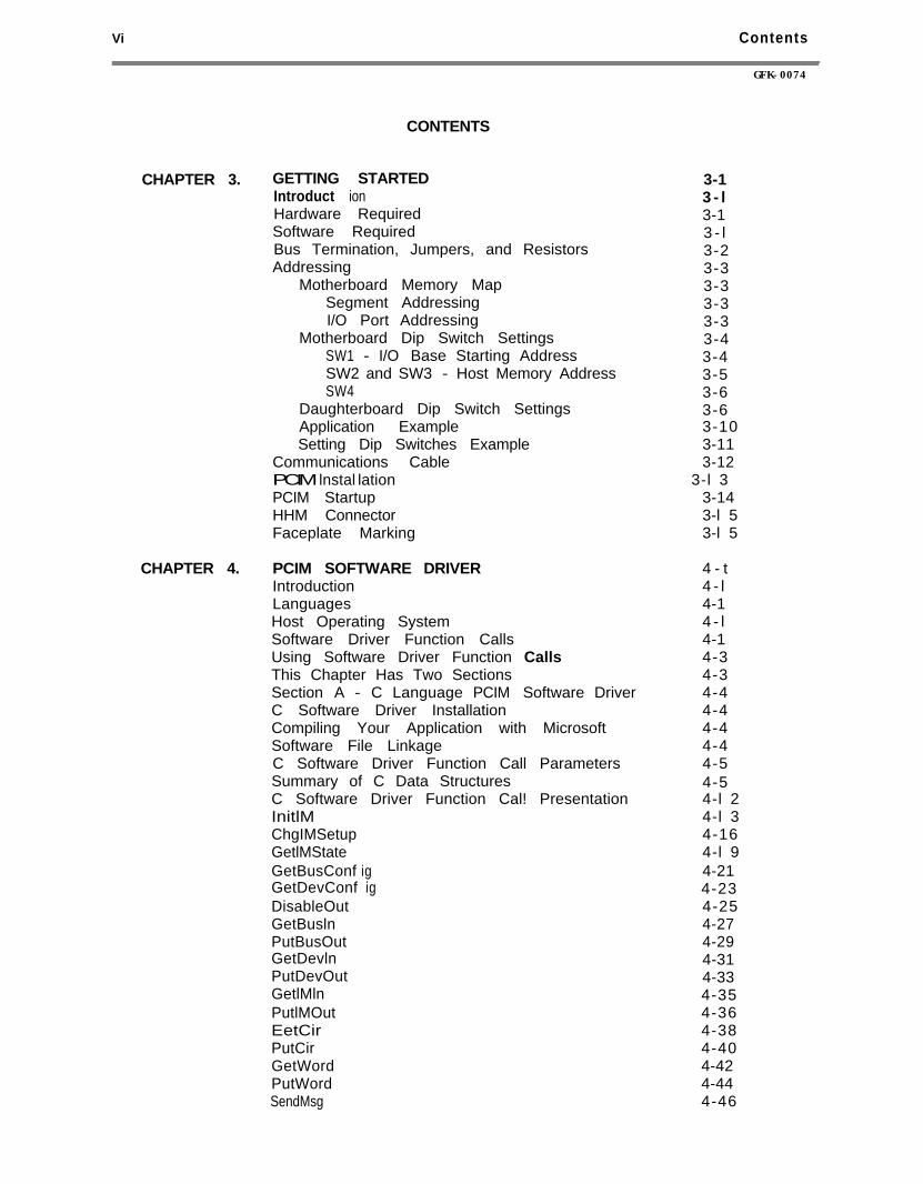
CONTENTS
CHAPTER 1. INTRODUCTlONGenius I/O System OverviewGenius I/O IBM PC Interface Module (PCIM)DaughterbaardGenius l/O IBM PC Interface Module (PCIM)Motherboard
CHAPTER 2. THEORY OF OPERATIONIntroductionPCIM Hardware Description
PCIM Motherboard Physical StructurePCIM Daughterboard Physical Structure
PCIM Hardware OperationSerial InterfaceData BufferHost Interface
PCIM Software OperationSerial Interface
Software FunctionalityPower Up And InitializationSteady State Operation
PCIM ManagerSoftware Functionality
Power Up And lnitializat ionSteady State Operation
Shared RAM InterfaceShared Ram UpdatesDevice Log InDevice Log OutMemory ConfigurationI/O Table LockoutDevice I/O TableInput TableOutput TablePCIM Broadcast Control Output TablePCIM Directed Control Input TableDevice Configuration TablePCIM Setup TablePCIM Status TableInterrupt Tables
PCIM Motherboard OperationWatchdog T imerPower Supply Voltage Detector and ResetCircuit
Reset Restrict ionsHost System Interrupt Control
PCIM Electrical CharacteristicsPower Supply RequirementsBus Loads/Drive Capabi Ii tySignal Conditioning
l - ll - l
l - 3
1-3
2 - l2-12-12 - l2 - l2-32-32-52-62-72-72-72-72-82-l 02-l 02-l 02-l 22-l 42-142-142-l 42-l 42-l 72-172-172-172-l 82-182-182-182-l 82-192-202-21
2-212-212-212-222-222-222-22
Vi Contents
GFK-0074
CONTENTS
CHAPTER 3. GETTING STARTED 3-1Introduct ion 3 - lHardware Required 3-1Software Required 3 - lBus Termination, Jumpers, and Resistors 3-2Addressing 3-3
Motherboard Memory Map 3-3Segment Addressing 3-3I/O Port Addressing 3-3
Motherboard Dip Switch Settings 3-4SW1 - I/O Base Starting Address 3-4SW2 and SW3 - Host Memory Address 3-5SW4 3-6
Daughterboard Dip Switch Settings 3-6Application Example 3-10Setting Dip Switches Example 3-11
Communications Cable 3-12PCIM lnstal lation 3-l 3PCIM Startup 3-14HHM Connector 3-l 5Faceplate Marking 3-l 5
CHAPTER 4. PCIM SOFTWARE DRIVERIntroductionLanguagesHost Operating SystemSoftware Driver Function CallsUsing Software Driver Function CallsThis Chapter Has Two SectionsSection A - C Language PCIM Software DriverC Software Driver InstallationCompiling Your Application with MicrosoftSoftware File LinkageC Software Driver Function Call ParametersSummary of C Data StructuresC Software Driver Function Cal! PresentationInitlMChgIMSetupGetlMStateGetBusConf igGetDevConf igDisableOutGetBuslnPutBusOutGetDevlnPutDevOutGetlMlnPutlMOutEetCirPutCirGetWordPutWordSendMsg
4 - t4 - l4-14 - l4-14-34-34-44-44-44-44-54-54-l 24-l 34-164-l 94-214-234-254-274-294-314-334-354-364-384-404-424-444-46
Contents vi i
GFK-0074
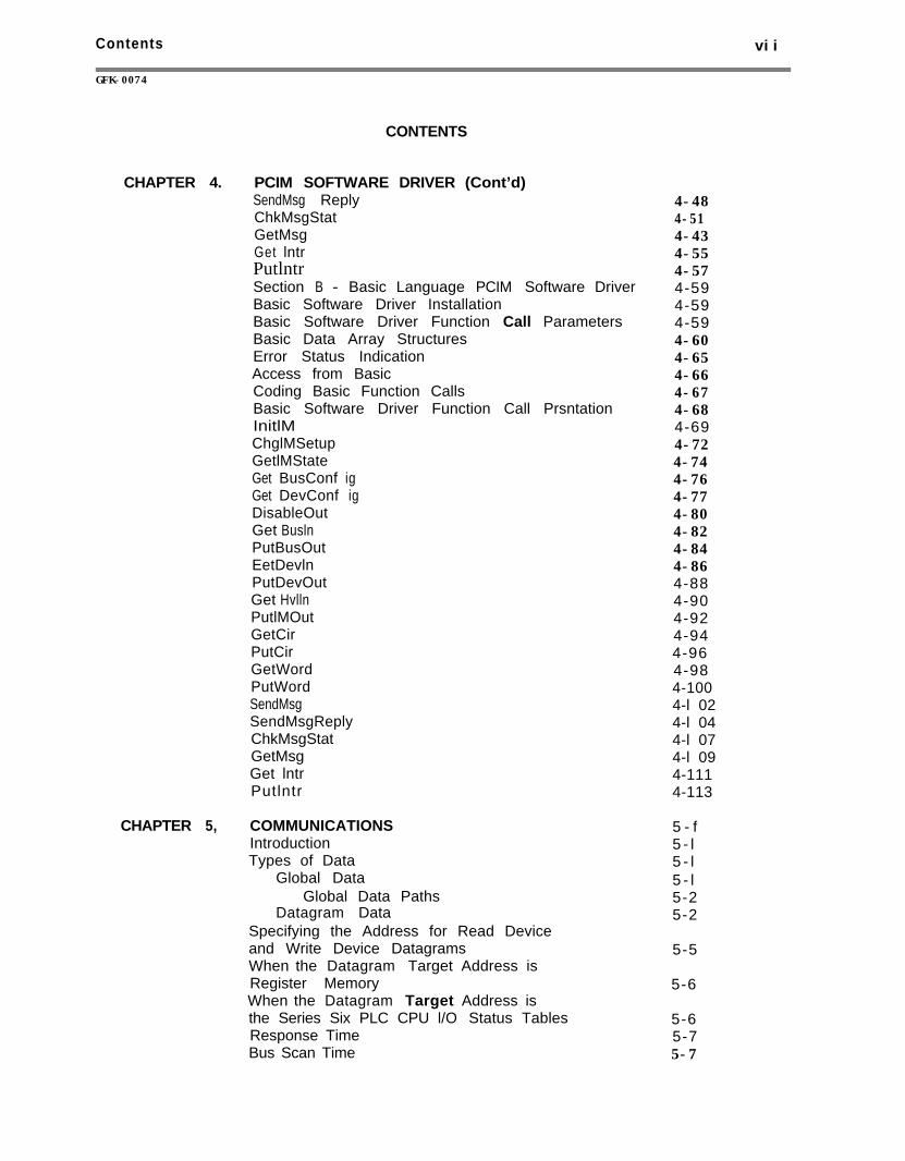
CONTENTS
CHAPTER 4. PCIM SOFTWARE DRIVER (Cont’d)SendMsg ReplyChkMsgStatGetMsgGet lntrPutlntrSection B - Basic Language PCIM Software DriverBasic Software Driver InstallationBasic Software Driver Function Call ParametersBasic Data Array StructuresError Status IndicationAccess from BasicCoding Basic Function CallsBasic Software Driver Function Call PrsntationInitlMChglMSetupGetlMStateGet BusConf igGet DevConf igDisableOutGet BuslnPutBusOutEetDevlnPutDevOutGet HvllnPutlMOutGetCirPutCirGetWordPutWordSendMsgSendMsgReplyChkMsgStatGetMsgGet lntrPutlntr
CHAPTER 5, COMMUNICATIONSIntroductionTypes of Data
Global DataGlobal Data Paths
Datagram DataSpecifying the Address for Read Deviceand Write Device DatagramsWhen the Datagram Target Address isRegister MemoryWhen the Datagram Target Address isthe Series Six PLC CPU l/O Status TablesResponse TimeBus Scan Time
4-484-514-434-554-574-594-594-594-604-654-664-674-684-694-724-744-764-774-804-824-844-864-884-904-924-944-964-984-1004-l 024-l 044-l 074-l 094-1114-113
5 - f5 - l5 - l5 - l5-25-2
5-5
5-6
5-65-75-7
v i i i Contents
GFK-0074
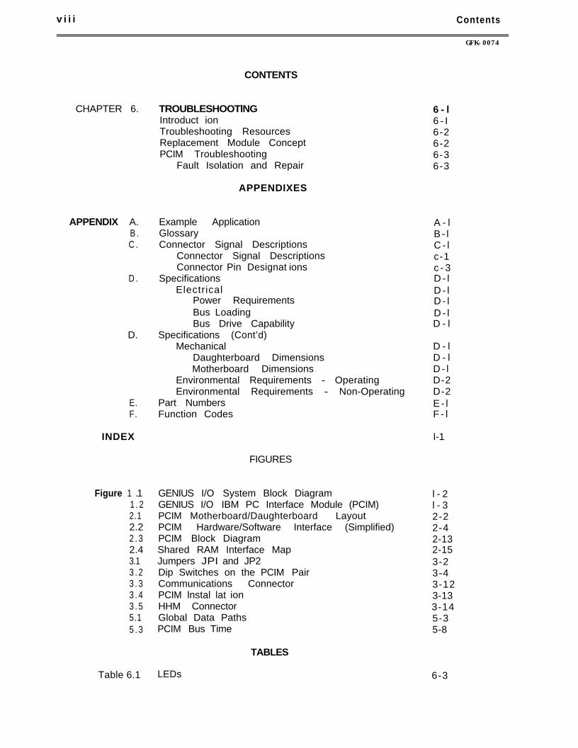
CHAPTER 6.
APPENDIX A.B .C .
D .
D.
E.F.
INDEX
Figure 1 .1 GENIUS I/O System Block Diagram l - 21 . 2 GENIUS I/O IBM PC Interface Module (PCIM) l - 32.1 PCIM Motherboard/Daughterboard Layout 2-22.2 PCIM Hardware/Software Interface (Simplified) 2-42 . 3 PCIM Block Diagram 2-132.4 Shared RAM Interface Map 2-153.1 Jumpers JPI and JP2 3-23 . 2 Dip Switches on the PCIM Pair 3-43 . 3 Communications Connector 3-123 . 4 PCIM lnstal lat ion 3-133 . 5 HHM Connector 3-145.1 Global Data Paths 5-35 . 3 PCIM Bus Time 5-8
Table 6.1
CONTENTS
TROUBLESHOOTlNG 6 - lIntroduct ion 6 - ITroubleshooting Resources 6-2Replacement Module Concept 6-2PCIM Troubleshooting 6-3
Fault Isolation and Repair 6-3
APPENDIXES
Example ApplicationGlossaryConnector Signal Descriptions
Connector Signal DescriptionsConnector Pin Designat ions
SpecificationsElectrical
Power RequirementsBus LoadingBus Drive Capability
Specifications (Cont’d)Mechanical
Daughterboard DimensionsMotherboard Dimensions
Environmental Requirements - OperatingEnvironmental Requirements - Non-Operating
Part NumbersFunction Codes
A - lB - lC - lc-1c - 3D - lD - lD - lD - lD - l
D - lD - lD - lD-2D-2E - lF - l
I-1
FIGURES
TABLES
LEDs 6-3
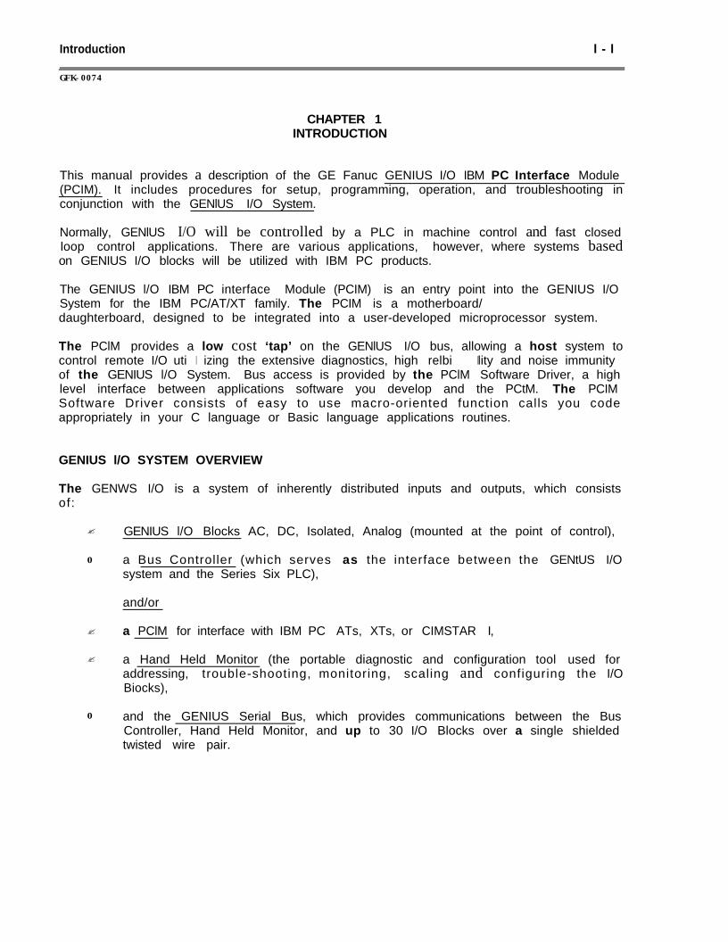
Introduction
GFK-0074
l - l
CHAPTER 1INTRODUCTION
This manual provides a description of the GE Fanuc GENIUS I/O IBM PC Interface Module(PCIM). It includes procedures for setup, programming, operation, and troubleshooting inconjunction with the GENlUS I/O System.
Normally, GENlUS I/O will be controlled by a PLC in machine control and fast closedloop control applications. There are various applications, however, where systems basedon GENIUS I/O blocks will be utilized with IBM PC products.
The GENIUS l/O IBM PC interface Module (PCIM) is an entry point into the GENIUS I/OSystem for the IBM PC/AT/XT family. The PCIM is a motherboard/daughterboard, designed to be integrated into a user-developed microprocessor system.
The PClM provides a low cost ‘tap’ on the GENlUS I/O bus, allowing a host system tocontrol remote I/O uti I izing the extensive diagnostics, high relbi Ility and noise immunityof the GENIUS l/O System. Bus access is provided by the PClM Software Driver, a highlevel interface between applications software you develop and the PCtM. The PCIMSoftware Driver consists of easy to use macro-oriented function calls you codeappropriately in your C language or Basic language applications routines.
GENIUS l/O SYSTEM OVERVIEW
The GENWS I/O is a system of inherently distributed inputs and outputs, which consistsof:
? GENIUS l/O Blocks AC, DC, Isolated, Analog (mounted at the point of control),
0 a Bus Controller (which serves as the interface between the GENtUS I/Osystem and the Series Six PLC),
and/or
? a PClM for interface with IBM PC ATs, XTs, or CIMSTAR I,
? a Hand Held Monitor (the portable diagnostic and configuration tool used foraddressing, trouble-shooting, monitoring, scaling and configuring the I/OBiocks),
0 and the GENIUS Serial Bus, which provides communications between the BusController, Hand Held Monitor, and up to 30 I/O Blocks over a single shieldedtwisted wire pair.
l - 2 Introduction
GFK-0074
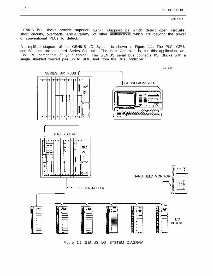
GENIUS l/O Blocks provide superior, built-in Diagnost ics which detect open circuits,short circuits, overloads, and a variety of other malfunctions which are beyond the powerof conventional PLCs to detect.
A simplified diagram of the GENIUS I/O System is shown in Figure 1.1. The PLC, CPU,and I/O rack are standard Series Six units. The Host Controller is, for this application, anIBM PC compatible of your choice. The GENIUS serial bus connects I/O Blocks with asingle shielded twisted pair up to 2000 feet from the Bus Controller.
SERIES SIX PLUS (
a41142
0 0 0 0 0
1-
0 0 0 0,c
1 GE WORKMASTER.
I
I SERIES SIX I/O
HAND HELD MONITOR
I- BUS CONTROLLER
I/0BLOCKS
Figure 1.1 GENIUS I/O SYSTEM DIAGRAM
Introduction 1 - 3
GENIUS I/O IBM PC INTERFACE MODULE (PCIM)
Daughterboard
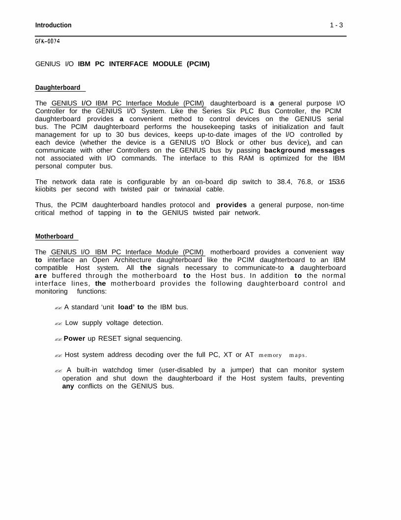
The GENIUS I/O IBM PC Interface Module (PCIM) daughterboard is a general purpose I/OController for the GENIUS I/O System. Like the Series Six PLC Bus Controller, the PCIMdaughterboard provides a convenient method to control devices on the GENIUS serialbus. The PCIM daughterboard performs the housekeeping tasks of initialization and faultmanagement for up to 30 bus devices, keeps up-to-date images of the l/O controlled byeach device (whether the device is a GENIUS t/O Block or other bus device), and cancommunicate with other Controllers on the GENIUS bus by passing background messagesnot associated with I/O commands. The interface to this RAM is optimized for the IBMpersonal computer bus.
The network data rate is configurable by an on-board dip switch to 38.4, 76.8, or 153.6kiiobits per second with twisted pair or twinaxial cable.
Thus, the PCIM daughterboard handles protocol and provides a general purpose, non-timecritical method of tapping in to the GENIUS twisted pair network.
Motherboard
The GENIUS I/O IBM PC Interface Module (PCIM) motherboard provides a convenient wayto interface an Open Architecture daughterboard like the PCIM daughterboard to an IBMcompatible Host system. All the signals necessary to communicate-to a daughterboardare buffered through the motherboard to the Host bus. In addition to the normalinterface lines, the motherboard provides the following daughterboard control andmonitoring functions:
?? A standard ‘unit load’ to the IBM bus.
?? Low supply voltage detection.
?? Power up RESET signal sequencing.
?? Host system address decoding over the full PC, XT or AT memory maps.
?? A built-in watchdog timer (user-disabled by a jumper) that can monitor systemoperation and shut down the daughterboard if the Host system faults, preventingany conflicts on the GENIUS bus.
l-4 Introduction
GfK-0074
b41682
Figure 1.2 GENIUS I/O IBM PC INTERFACE MODULE (PCIM)
Theory of Operation 2 - l
CHAPTER 2THEORY OF OPERATION
INTRODUCTION
This chapter explores the physical configuration/operation of the PCIM, and provides adescription of module general capabilities. PCIM physical structure is described in thefirst sect ion. PCIM hardware, functionally divided into three primary sections, isdiscussed in the second section. PCIM software is functionally divided into twosubsystems; explained in the following sect ion. PCIM motherboard functions are brieflydiscussed next, followed by a definition of electrical and signal requirements.
You need not be familiar with the material presented in chapter 2 in order to operateyour PCIM. If you aren’t interested in how it works, just go on to chapter 3.
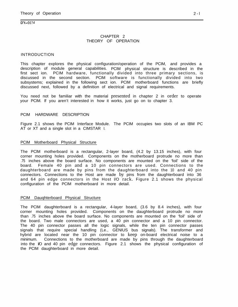
PCIM HARDWARE DESCRIPTION
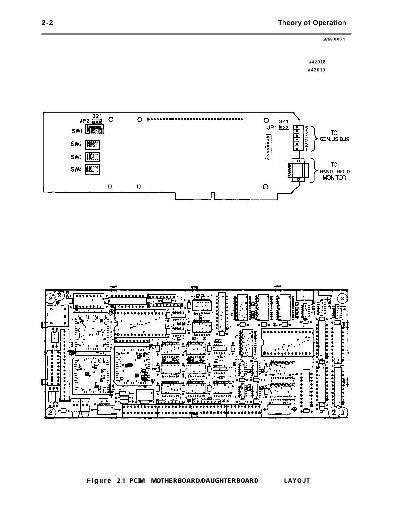
Figure 2.1 shows the PCIM Interface Module. The PCIM occupies two slots of an IBM PCAT or XT and a single slot in a CIMSTAR I.
PCIM Motherboard Physical Structure
The PClM motherboard is a rectangular, 2-layer board, (4.2 by 13.15 inches), with fourcorner mounting holes provided. Components on the motherboard protrude no more than.75 inches above the board surface. No components are mounted on the ‘foil’ side of theboard. Female 40 pin and a 10 pin connectors are used. Connections to thedaughterboard are made by pins from the daughterboard into the 10 and 40 pinconnectors. Connections to the Host are made by pins from the daughterboard into 36and 64 pin edge connectors in the Host l/O rack. Figure 2.1 shows the physicalconfiguration of the PCIM motherboard in more detail.
PCIM Dauqhterboard Physical Structure
The PCIM daughterboard is a rectangular, 4-layer board, (3.6 by 8.4 inches), with fourcorner mounting holes provided. Components on the daughterboard protrude no morethan .75 inches above the board surface. No components are mounted on the ‘foil’ side ofthe board. Two male connectors are used, a 40 pin connector and a 10 pin connector.The 40 pin connector passes all the logic signals, while the ten pin connector passessignals that require special handling (Le., GENIUS bus signals). The transformer andhybrid are located near the 10 pin connector to keep on-board electrical noise to aminimum. Connections to the motherboard are made by pins through the daughterboardinto the I/O and 40 pin edge connectors. Figure 2.1 shows the physical configuration ofthe PCIM daughterboard in more detail.
2-2 Theory of Operation
GFK-0074
a42018
a42019
JP2& 0 Oh ooooooo~oooooooboooo#o*ooooooo
SW11 rRnillulo 0 5
SW2 mmIswspiiiiiq
SW4 jiiiiiq
0 0
To~GENIUSBUS
ToHAND-HELDWiTOR
Figure 2.1 PCIM MOTHERBOARD/DAUGHTERBOARD LAYOUT
Theory of Operation 2-3
GFK-0074
PCIM HARDWARE OPERATION
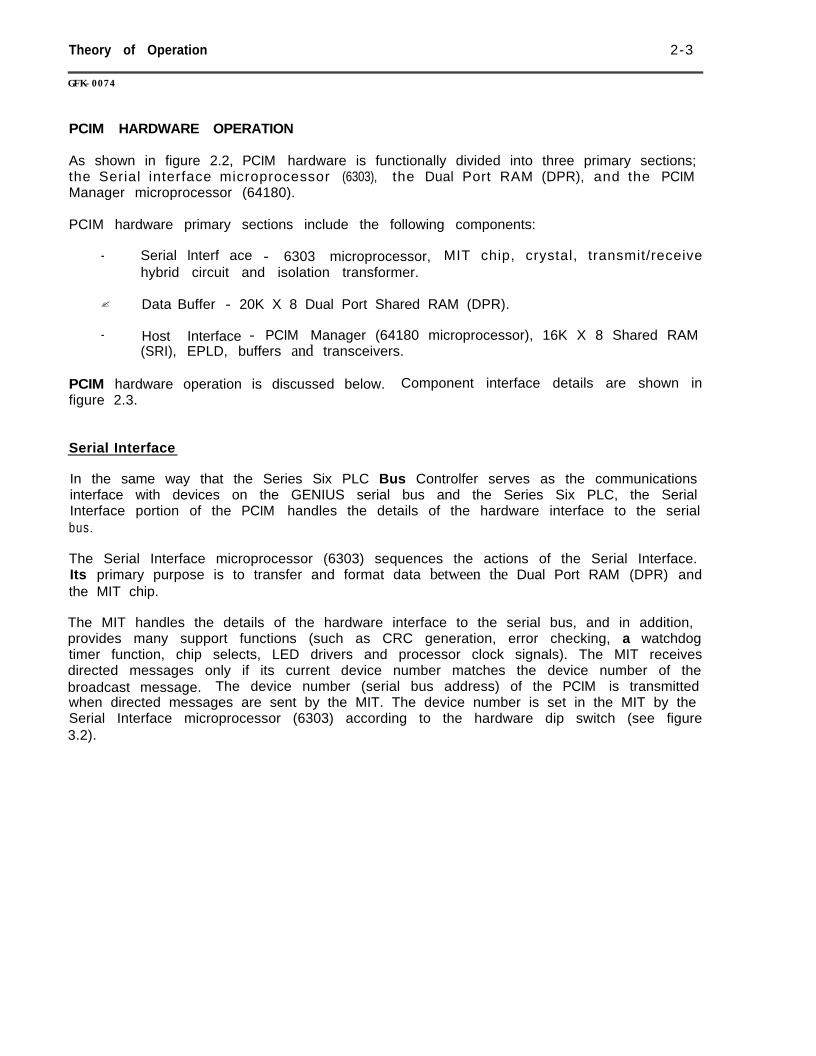
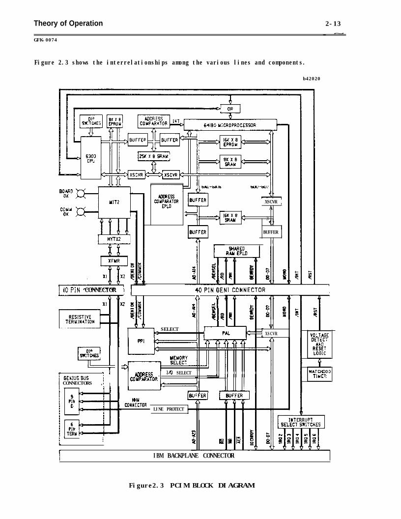
As shown in figure 2.2, PCIM hardware is functionally divided into three primary sections;the Serial interface microprocessor (6303), the Dual Port RAM (DPR), and the PCIMManager microprocessor (64180).
PCIM hardware primary sections include the following components:
- Serial lnterf ace - 6303 microprocessor, MIT chip, crystal, transmit/receivehybrid circuit and isolation transformer.
? Data Buffer - 20K X 8 Dual Port Shared RAM (DPR).
- Host Interface - PCIM Manager (64180 microprocessor), 16K X 8 Shared RAM(SRI), EPLD, buffers and transceivers.
PCIM hardware operation is discussed below. Component interface details are shown infigure 2.3.
Serial Interface
In the same way that the Series Six PLC Bus Controlfer serves as the communicationsinterface with devices on the GENIUS serial bus and the Series Six PLC, the SerialInterface portion of the PCIM handles the details of the hardware interface to the serialbus.
The Serial Interface microprocessor (6303) sequences the actions of the Serial Interface.Its primary purpose is to transfer and format data between the Dual Port RAM (DPR) andthe MIT chip.
The MIT handles the details of the hardware interface to the serial bus, and in addition,provides many support functions (such as CRC generation, error checking, a watchdogtimer function, chip selects, LED drivers and processor clock signals). The MIT receivesdirected messages only if its current device number matches the device number of thebroadcast message. The device number (serial bus address) of the PCIM is transmittedwhen directed messages are sent by the MIT. The device number is set in the MIT by theSerial Interface microprocessor (6303) according to the hardware dip switch (see figure3.2).
2-4 Theory of Operation
SERIALBUS
1II
IMERFACE
GFK-0074
a42016
IM a n a g e r
MICROPROCESSORII
( 64180 )
l- ---------
IGENI II I
MANAGERI I
I 1 -I- - - - -
.------- -l
Figure 2.2 PCIM HARDWARE/SOFTWARE INTERFACE (SIMPLIFIED)
Theory of Operation 2-5
CFK-0074
The PClM Serial Interface also includes a transmit/receive hybrid circuit and atransformer. Serial Interface components work together to communicate with the serialbus and implement the following specific functions:
a Transmit messages to the serial bus using the serial bus protocol. Thesemessages are written to the transmit buffers in the MIT chip by the 6303microprocessor. When the MIT chip determines that it is its turn on the bus, itallows the messages in the transmit buffers to be transmitted. The hybridcircuit translates MIT transmit and receive signals levels to levels appropriatefor transmission on the serial bus. The transformer provides isolation betweenthe twisted pair wires and the PC/M circuitry.
- Receive messages from the serial bus. These messages are read from thereceive buffer in the MIT chip by the 6303 microprocessor.
- Manage an external clock for running the 64180 microprocessor.
? Control 2 LEDs which are used to indicate the status of the board (PCIM OK,COMM OK, diagnostic faults).
- Allow two chip selects - one for the 6303 microprocessor and one for accessingthe Dual Port RAM (DPR).
- Permit a watchdog timer function for the PCIM.
Data Buffer
The Dual Port RAM (DPR) is the area where the PCIM Manager microprocessor (64180)and the Serial Interface microprocessor (6303) exchange data. This hardware allows the2OK Dual Port RAM to be accessed simultaneously without loss of data. The DPR, then,is arranged to prevent conflicts when both microprocessors try to move data through theRAM at the same time. In a manner similar to the arbitration used between the PClMManager and the Host Shared RAM (SRI), the Dual Port RAM is controlled by an EPLD,which arbitrates memory requests on a byte-by-byte basis. The EPLD actually controlsthe buffers and transceivers each microprocessor uses to read or write from/to the SharedRAM. Thus, the Dual Port RAM removes any timing skews between the two processorswhich are running two separate, asynchronous systems.

2-6 Theory of Operation
Host Interface
l-lost Interface hardware allows the Shared RAM Interface (SRI) to be accessed by eitherthe PCIM Manager microprocessor (64180) or the Host system without a loss of data. ThePCIM Manager microprocessor (64180) transfers data between the Shared RAM Interface(SRI) and the Serial Interface microprocessor (6303) through the Dual Port RAM (DPR).
Either source can access the SRI simultaneously, byte-by-byte, without worrying aboutsoftware arbitration. The hardware arbitrates requests for the Shared RAM interface andkeeps the timing straight. As a result, the SRI looks like a pure RAM device to bothsystems. If the Host requires that more than one byte of data be transferred without anyintermediate byte accesses from the PCIM, a software lockout scheme is used. Theinterface signals are directly compatible with those of the PC backplane.
The PCIM Manager microprocessor (64180) sequences the actions of the PCIM Manager,whose primary purpose is to transfer and format data between the Shared RAM Interface(SRI) and Dual Port RAM (DPR) by executing a program located in the EPROM.
In addition, the PCIM Manager generates an interrupt when important information hasbeen deposited into the SRI. When the Host desires to write or read grouped multi-bytedata, it can request a lock out of the Shared RAM. The Host initiates this lock out bywriting the request in the Command byte of the SRI, which causes an interrupt for thePCIM Manager. The PCIM Manager acknowledges the interrupt by setting a bit in the SRIand pulsing the interrupt line to the Host.
The Shared RAM interface (SRI) is the user’s interface to the PCIM. An EPLD arbitratesShared RAM memory requests on a byte-by-byte basis and allows the Host and PCIMManager equal simultaneous access to any byte of Shared RAM without loss of data. TheSRI contains 16K bytes for I/O tables, configuration data, diagnostic data, labels andbackground message queues.
Theory of Operation
GFK-0074
2-7
PCIM SOFTWARE O p e r a t i o n
PCIM software is functionally divided into two subsystems:
- Serial Interface software.
? PCIM Manager software.
The Serial interface software provides the interface to the GENIUS serial bus from theDual Port RAM (DPR), the shared RAM area between the Serial Interface and the PCIMManager. PCIM Manager software primarily interfaces and formats data from the DualPort RAM area into the Shared RAM Interface (SRI), the shared RAM area between thePCIM Manager and the Host system.
Serial Interface
The primary responsibil ity of the the Serial Interface portion of PCIM software isGENIUS l/O Network Protocol. The Serial Interface handles keeping the PCIM active onthe GENIUS serial bus. Since the PCIM is a control device, it must be able to receivecontrol data from all devices on the bus and must be able to direct control data to anygiven station on the bus.
The secondary function of the Serial interface software is to maintain the overalloperation of the PCIM. This is accomplished by servicing the MIT watchdog timer andmaintaining a ‘heartbeat’ with the PCIM Manager. If any of these fail, then the SerialInterface generates a reset signal and the PCIM becomes inactive.
Serial Interface Software Functionality
Power Up and Initialization
When power is applied to the PCIM, the Serial Interface begins performing power upinitialization. The following set of circuitry/hardware power up diagnostic tests are run:
? EPROM Checksum Test
- Microprocessor Self Check Test
- MIT Bus lest
- RAM Test
If any of the tests fail, the software attempts to go into a controlled lock-up statepreventing the PCIM from running at all. If the diagnostics pass, the Serial Interfacecompletes initialization of its memory variables, Dual Port RAM, the MIT and otherhardware or software related variables necessary to begin steady state operation.
2-8 Theory of Operation
GFK-0074
The Serial Interface will read--the hardware dip switch (see figure 3.2) one time duringpower up. Information received from the dip switch will be provided to the PCIMmanager via the Dual Port RAM. The dip switch setting will be ignored at all other times.
The Serial Interface will next initialize the MIT. During initialization, the MIT will alsobe set with the serial bus address of the PCIM and the serial bus baud rate (whenavailable). The address and the baud rate are derived from the dip switch setting. TheSerial Interface will complete the MIT initialization and begin transmitting its token onthe serial bus.
The Serial Interface makes the value of the on-board dip switch setting available to thePCIM Manager software. This value indicates the serial bus address of the PCIM and thedefault output disable flags. The Serial Interface may begin collecting input control datafrom the bus but will not transmit output control data until there is data to transmit.
Steady State Operation
During normal operation, the Serial Interface software is required to provide thefollowing functions for the PCIM Manager software:
? Maintain a Dual Port RAM table of control inputs from all devices on the busfor the PCIM Manager. Maintain an information queue of device addresseswhich sent input data.
- Inform the PCIM Manager whenever new control data from any bus device isreceived.
- Maintain a queue of incoming datagram messages in the Dual Port RAM for thePCIM Manager to act on.
- Transmit the following message types when it is the PCIM’s turn to access theserial bus; ,
0 Of 1 Direct or Broadcast Background Message0 to 31 Directed Control Message
1 Broadcast Control Message (token)
? Direct control data outputs to individual bus devices as grouped data. Theseoutputs will be maintained in the Dual Port RAM by the PCIM Manager.
- Maintain an information queue of device addresses to which the PCIM sentoutput data. Inform the PCIM Manager when each output is sent via this queue.
Theory of Operation 2-9
Send datagram messages from a single message buffer as a Directed orBroadcast Background Message in either restricted or unrestricted mode. Thissingle message buffer is maintained by the PCIM Manager in the Dual PortRAM.
Reinitialize the MIT chip to support the two priority classes of DatagramService - NORMAL and HIGH Priority.
Inform the PClM Manager whenever new control data for all bus devices isreceived from the serial bus.
Inform the PCIM Manager whenever a datagram message is received from theserial bus.
Interrupt the PCIM Manager each time the PCIM completes its turn on the bus.
Maintain a minimum serial bus scan time of 3 ms.
Stop any transmission on the serial bus on command from the PCIM Managerfor a time period of 1.5 seconds.
Report the bus scan time in milliseconds to the PCIM Manager every scan.
Maintain a running count of serial bus errors.
Implement a watchdog timer service routine.
Continuously run a series of background diagnostic tests which verify its ownlocal RAM and its EPROM (checksum).
Detect a fatal failure with the PCIM Manager in order to cause the PCIM tohalt.
Inform the PCIM Manager of a fatal failure with the Serial Interface, and allowtime for the PCIM Manager to report this to the host before causing the tohalt.
Maintain the LED indicators PCIM OK and COMM OK. If the PCIM Manager’sheartbeat fails or any of the diagnostics fail, turn off the PCIM OK LED. If aserial bus error occurs, turn off the COMM OK LED for 200 msec. If the PCIMdoes not get a turn on the bus within the allotted time period dependant on thebaud rate, turn off the COMM OK LED. In this last case, the LED will remainoff until the PC IM gets its turn on the bus.
2-10 Theory of Operation
GFK-0074
PCIM Manager
The basic function of the PCIM Manager is to provide data flow between the serial busand the Host via a formatted shared RAM interface. Key functions of the PCIM Managerinclude:
? transfer of sampled data (I/O or Global Data Services) to and from otherdevices on the bus. This data is for basic I/O devices, or global data which isshared between other types of devices such as processors
- transfer of unique data (Datagram Service) to and from other bus devices, Thisdata includes configuration, diagnostic and other types of unique data
- maintenance of device characteristics in a Configuration Table
device, PCIM, bus and syntax error reporting
PCIM Manager Software Functionality
Power Up and Initialization
When the Host is ready to use the PClM function, it allows the PCIM to be reset. TheSerial Interface then begins its power up sequence. Again, when the Serial Interfacecompletes its power up and diagnostics, the PClM Manager can begin operation.
During power up, the PClM Manager performs diagnostic tests on all of its relatedhardware. These tests include:
- EPROM Checksum Test
? Microprocessor Test
- RAM Test
If an error is found in any of the diagnostics, the PCIM Manager reports the fault to theHost through the PCIM Status, then attempts to halt. The host will not be given a PClMOK status, nor will the PCIM OK LED Ilight.

Theory of Operation 2-11
GFK-0074
If all diagnostic tests pass, the PCIM Manager then initializes its operating variables.The Loss of Device Timeout will be set to 3 bus scans. The Shared RAM variables will bedefaulted as fol lows:
Device Present
Output Disable
Serial Bus Address
Serial Bus Baud Rate
l/O Table Lockout State
Broadcast Control Data Length
Directed Control Data Length
I/O Table Length
Status Table Address
A l l i n t e r r u p t S t a t u s
All interrupt D i s a b l e
All PCIM S t a t u s
=o
setting based on daughterboard dipswitch
setting based on .daughterboard dipswitch
setting based on daughterboard dipswitch
= o
= o
= o
= 128 (80 hex)
= OFFFF (hex)
= o
= o
= o
Receive Queue, Transmit Buffer,Request Queue = empty
Command Block Status Byte = Command Complete
During the PCIM Manager’s power up sequence, the Host must not read or write to theShared RAM for 1.7 seconds. After 1.7 seconds, the PCIM OK flag should be ONindicating self-test has passed (the PCIM sets the state of the PCIM OK byte to ‘1’ withintwo seconds after power up).
The Serial Interface will not write to the Dual Port RAM or begin transmitting on the busuntil the PCtM Manager informs it that power up processing has been successfullycompleted.
Once the PCIM OK flag is set to ‘I’, the PCIM Manager will delay an additional 1.5seconds to allow the Host to change the PCIM default configuration. Since the PCIMdrops off of the bus after a configuration change, this feature allows the host to changeconfiguration before any bus activity begins.
2-l 2 Theory of Operation
GFK-0074
Steady State Operation
From this point, the PCIM Manager runs in steady state operation. Operation of thePCIM Manager is closely related to that of the Shared RAM Interface, including;
Self -Test - During steady state operation, the PCIM Manager is required to performbackground diagnost ics. These tests include a non-destructive private RAM test, achecksum of the EPROM, and maintainenance of a heartbeat with the Serial Interface. Ifany faults are found in these background diagnostics, the PCIM Manager reports the faultthrough the PCIM Status area of the Shared RAM, disable outputs to the serial bus, andthen attempt to halt all processing.
I/O Table Lockout - To ensure data coherency for all control data to and from the Host,the PCIM Manager will implement a ‘lockout’ of all control data tables during an I/OLockout Request. During I/O Table Lockout, the PCIM Manager will NOT access theInput Tables, the Output Tables, the Broadcast Control Output Table and the DirectedControl input Table.
Host Interrupts - There are seven conditions requiring immediate Host attention whichcauses the PCIM Manager to interrupt the Host. Before interrupting the Host, the PCIMManager will set the interrupt condition in the Interrupt Status Table of the SRI bywriting a ‘1’ to the byte indicating the interrupt condition. The i-lost w i II clear theInterrupt Status Table entry when it has completed servicing that interrupt.
The Host may disable any of the seven interrupt conditions via the Interrupt DisableTable. When the PCIM Manager determines that one of the interrupt condition exists,that byte in the Interrupt Status Table is set. Then, the Interrupt Disable Table will beinterrogated. If the corresponding disable flag is set, no interrupt will be generated tothe HOST. The HOST will still be responsible for clearing the corresponding byte in theInterrupt Status Table (see chapter 4).
Whenever control data is received, the PCIM Manager will determine if that particulardevice is already ‘logged’ into the Configuration Table. If so, the PCIM Manager acceptsthe control data and places it into the Input Table. If not, the PCIM Manager requestscontrol data parameters from that device. The control data is ignored until theseparameters are received by the PCIM Manager.
Theory of Operation 2-13.-. .~
GFK-0074
Figure 2.3 shows the interrelationships among the various lines and components.
b42020
,XSCVR 1A
KKK8 <SRAU 3
BUFFER
I I
cDEi;DR
IOPIpi CONNECTOR
VXSCVR
1 1 n #EpZSII;it!
2: dII I8P
+% SELECT It +
DlPswmHEsQ=L
MDRESS . l/U SELECT?
WYPARATDR, I
GENIUSBUS 1CONNECTORS , I
COlltinEYtTDRLINE PROTECT
I Ii
I IBM BACKPLANE CONNECTOR
Figure2.3 PCIM BLOCK DIAGRAM

2-l 4 Theory of Operation
SHARED RAM INTERFACE
As you remember, all data passed between the Host system and the. PCIM goes throughHost shared RAM, referred to as the Shared RAM Interface (SRI). As stated, this RAMlooks like an 16Kx8 static memory device to the Host system. Although all areas of RAMare ‘read/write’, that is, fully accessible by the Host to read or write to any RAMlocation, some areas of the RAM are not accessed by the Software Driver during normaloperation (as shown in figure 2.4).
Shared RAM Updates
Some data is transferred between the Shared RAM and the serial bus automatically by thePCIM manager. This type of communication includes I/O circuit updates, fault reports,and the like. The rest of the calls and message types must be initiated by the Hostsystem using the Software Driver, explained in more detail in chapter 4.
Device tog In
The PCIM Manager will log in a device whenever control data is received from a devicethat is NOT listed in the Host’s SRI. A device is considered logged in, or on-line, whenthe PCIM Manager has that device’s configuration data translated and stored in the SRI (aGetBusConfig call can be used to verify the presence of the device on the bus). At thispoint, the device is considered logged in and input control data from that device will betransferred to the SRI Input Table.
Heavy log in activity occurs after power up of the PCIM Manager if there are no deviceslogged in the SRI. Once in steady state, Jog in activity occurs whenever BroadcastControl data is received from a device that has just been included on the serial bus.
You may want to code the InitlM call (see chapter 4) in your program logic first (in orderto allow devices on the bus to log in with the PCIM), and then perform the rest of yourprogram logic initializations in order to optimize front-end timing.
Device Log Out
The PClM Manager will log a device out whenever Broadcast Control data is not receivedfor three (3) consecutive serial bus scans. This timeout period is fixed by the PCIMManager. When Device Log Out occurs, the PCIM Manager will not direct output data tothat device from the Serial Interface, and will inform the Host of the Loss of Device.
The device remains logged off until the PCIM Manager receives identification data fromit. When new Broadcast Control data is received from any device which is not logged in,the PCIM Manager will begin its device log in procedure.
Memory Configuration
Following is the memory map for the PCIM 16K Shared RAM Interface. It shows thedifferent areas used to convey data, status, control and diagnostic information to andfrom the Host system. A complete map of the Shared RAM Interface is shown in figure2.4.

Theory of Operation 2-15
GFK-0074
Request Queue
16 X 136 (2176)
R e q u e s t Q u e u e *Head Pointer
(1)
Request QueueTail Pointer
(1)
PCIM SetupTable
(16)
PCIM StatusTable
(16)
interrupt StatusTable
(16)
Interrupt DisableTable
(16)
Command B lock *
(16)
Output Data Area
(240)
Serial Bus accessto Host memory
Pointer to buffert-lost is reading
Pointer to bufferPCIM i s w r i t i ng
PCIM and Serial BusCharacteristics
PCIM and Serial BusDiagnostics
Host interrupts
DisableHost Interrupts
D r i v e r Calls t oPCtM Manager
Transmit DatagramBuffer RAM
* Host write to these locations causes Interrupt to the PCIM Manager
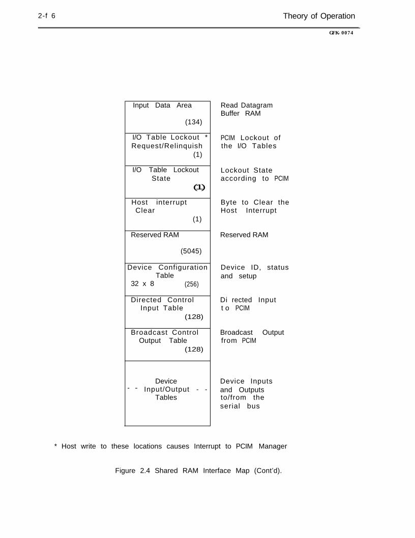
figure 2.4 Shared RAM Interface Map
2-f 6 Theory of Operation
GFK-0074
Input Data Area
(134)
I/O Table Lockout *Request/Relinquish
(1)
I/O Table LockoutState
(1)
Host interruptClear
(1)
Byte to Clear theHost Interrupt
Reserved RAM Reserved RAM
(5045)
Device ConfigurationTable
32 x 8 (256)
Directed ControlInput Table
(128)
Device ID, statusand setup
Di rected Inputt o PCIM
Broadcast ControlOutput Table
(128)
Broadcast Outputfrom PCIM
Device- - Input/Output - -
Tables
Read DatagramBuffer RAM
PCIM Lockout ofthe I/O Tables
Lockout Stateaccording to PCIM
Device Inputsand Outputsto/from theserial bus
* Host write to these locations causes Interrupt to PCIM Manager
Figure 2.4 Shared RAM Interface Map (Cont’d).
Theory of Operation 2-l 7
G F K - 0 0 7 4
I/O Table Lockout
To ensure data coherency for all control data to and from the Host, the PCN Managerwill implement a ‘lockout’ of all control data tables during an I/O Lockout Request. Thisfeature prevents the PClM Manager from accessing the SRI at the same time that theHost is updating it. Two bytes in the Shared RAM Interface (SRI) are dedicated to theI/O Lockout feature: I/O lockout Request/Relinquish, and t/O Table Lockout State.
The maximum response time to the t/O Table Lockout Request will be determined by thetime required for the PCIM Manager to transfer 128 bytes to or from the Input or OutputTable. Normally, the response will be less than this time. However, if the PCIM Manageris currently transferring data to or from the Input or Output Table, it will complete thecurrent data transfer before accepting and enabling the lockout. When the Host hascompleted its control data access, the PCIM Manager will resume normal operation inservicing control data to and from the SRI.
Device I/O Table
The Device l/O Table resides in the last 8K bytes of the Shared RAM memory and isdivided into two tables - the Device Input Table, and the Device Output Table (seechapter 5). The Input Table wili contain the Broadcast Control Data from each logged indevice. The input Table is updated every serial bus scan unless I/O Lockout is enabled.Data placed in the Output Table by the Host will be sent to each logged in device everyserial bus scan.
Both the Input and Output Tables are organized in groups of up to 32 segments each(corresponding to the maximum possible number of devices on the bus). Segment lengthsare fixed at 128 bytes.
Jnput Table
All Broadcast Controt Data will be placed in the Input Table in the segment associatedwith that particular device. That is, control data from device #I2 will be placed insegment 12. As such, the Input Table can be thought of as an array table. The Host willbe able to determine the type of I/O Block from the Device Configuration Table.
Output Table
The PClM Manager will take the data placed in the Output Table and direct that data tothe device associated with the given Output Table segment. If the Host wants to sendcontrol data to I/O Block #l2, it must place that data in segment 12 of the Output Table.As with the Input Table, the format of each individual segment is established in the lnitlMcall.
2-1 8 Theory of Operation
PCIM Broadcast Control Output Table
The PCIM Manager will transmit its own Broadcast Control Data onto the serial bus onceper scan. The Host will place data in the Broadcast Control Output Table for the PCIMManager to broadcast (see chapter 5).
PCIM Directed Control Input Table
The PCIM Manager may receive Directed Control Data from any device capable ofsending this type of message to the PCIM. The Directed Control Input Table is providedin the SRI for this data (see chapter 5).
Thus, a series of Hosts may be placed on a single bus and communicate with each other.Using the Broadcast Control Output Table, all PCIMs can broadcast control data to allother PClMs on that serial bus. Using the Directed Control input Table, a single PCIMcan be controlled by another PCIM. This a powerful feature of the PCIM Manager.
Device Configuration Table
The Device Configuration Table, 256 bytes long, contains the device ID, status, setup andother characteristics of each device connected to the serial bus controlled by this PCIM.Parameters are received by the PCIM Manager via an InitlM or ChglMSetup call. Thesetables are formatted into 32 segments of 8 bytes per segment. One 8 byte segment isreserved for each of the 32 possible devices, with the lowest, device number 0, residing inthe first 8 byte segment.
PCIM Setup Table
The PCIM Setup Table contains parameters unique to a particular PCIM. Theseparameters consist of device related values. When the Host changes one or more of theseparameters, the PCIM Manager will log all devices out of the database and drop all bustransmissions for 1.5 seconds, the time period necessary to cause all receiving devices tolog out the PCIM. When the PCIM begins re-transmitting, these devices will re-log in tothe PCIM with the new parameters.
PCIM Status Table
The PCIM Status Table contains six bytes indicating the veracity of the PCIM softwareand the status of the PCIM hardware. When certain status bits change, the PCIMManager will set the PCIM Status Change byte in the Interrupt Status Table. If thisinterrupt is not disabled, the PCIM Manager also will cause a Host interrupt to occur.interrupt Status will be set when for a RAM fault, an EPROM fault, or for excessive buserrors.
Theory of Operation 2-19
GFK-0074
Interrupt Tables
Several conditions occur which can cause the PCIM Manager to set a byte in the InterruptStatus Table, and possibly result in the generation of an interrupt for the Host. Thefollowing is an explanation of each condition:
- Interrupt Summary Status - Whenever the PClM Manager causes an interrupt tothe Host, the interrupt Summary Status byte will be set in the Interrupt StatusTable. If this byte is set in the Interrupt Disable Table, the PCIM Manager willnot interrupt the Host for any reason.
? Request Queue Entry - Certain messages received from devices on the bus willbe separated out from all other messages and placed in the Request Queue.The PCIM Manager will then set the Request Queue Entry byte.
- PCIM Status Change - When certain items within the PCIM Status Tablechange, the PCIM Manager will indicate this change by setting the PClM StatusChange byte.
- Device Status Change - Anytime that a device on the bus is logged in, loggedout or changes its configuration data, the PCIM Manager will set the DeviceStatus Change byte.
- Outputs Sent - This status byte is set whenever the PCIM relinquishes itsaccess to the serial bus. This interrupt status can be used to synchronize to theserial bus scan if required.
- Command Complete - Each time the Host initiates a command, and the PCIMManager completes that command (with or without errors), this status byte willbe set.
- Receive Queue Not Empty - Whenever any message is received from a deviceon the serial bus that is not part of Request Queue Entry, Serial Bus Requests,or a response from the command Transmit with Reply, this status byte will beset. Since these messages will be queued, the Host may retrieve them via theRead Datagram Command.
- I/O Table Lockout Grant - When the Host requests an l/O Table Lockout (not aRelinquish), this byte will be set to indicate when the PClM Manager is able toenforce the lockout. The lockout is not enforced until this byte is returned tothe Host.

2-20 Theory of Operation
GFK-0074
PCIM M O T H E R B O A R D O P E R A T I O N
The PCIM motherboard’s primary function is to provide an electrical interface betweenthe PCIM daughterboard and a Host system. The PCIM motherboard has no ‘smart’components and therefore will be functionally transparent to the user. The motherboarddoes, however, provide support features that enhance daughterboard functions and allowsthe PCIM to function as an IBM PC type I/O board.
The PCIM motherboard includes the following components:
a Address buffers
- Data transceiver
- Address decoders
? PAL logic control
- Programmable Peripheral interface
a Watchdog timer
a Power supply control
a Host interrupt control
? Signal conditioning
Pertinent PCIM motherboard hardware operation is discussed below. Componentinterface details are shown in figure 2.3.
Theory of Operation 2-21
GFK-0074
Watchdog Timer
The watchdog timer is a hardware timer that can be periodically reset and is used toreset the motherboard. if the watchdog timer is enabled by jumper JP2 (see figure 3.1),it must be reset periodically or it will put the PClM into RESET. You can toggle thewatchdog timer and use it as a failsafe timer to ensure that if the Host system ‘hangs up’,the PCIM will not send any erroneous messages to the serial bus. If the watchdog timer isdisabled by JP2, you do not have to toggle it; it will stay turned off and will not put thePCIM into RESET.
Power Supply Voltage Detector And RESET Circuit
In addition to the watchdog timer, the power supply voltage detector can put the PCIMinto RESET if it detects a low power supply voltage.
The RESET circuit monitors the system reset signal on the Host bus (called RESETDRVon an IBM type bus), as well as the output of the voltage detector and the watchdog timer.
Reset Restrictions
Do not enable interrupts, or read/write to the PCIM for 1.7 seconds (the period of timerequired for hardware/software init ialization) after reset. One false interrupt occurswithin this time period. Reading or writing to the PCIM during this time may cause thewatchdog timer to time out. The PCIM OK flag wilt be invalid during this period of time.
Host System Interrupt Control
The motherboard provides a method to interrupt the daughterboard and receive and routean interrupt request from the daughterboard to the Host system. The Host, using themotherboard, can interrupt the daughterboard by toggling the output line.
The daughterboard can also request an interrupt from the Host. The motherboard latchesthe edge of the interrupt where it can be read or routed through a selector switch (seefigure 2.3) to one of five interrupt request lines on the Host bus. The motherboard canreset the latch, readying it for the next interrupt.
2-22 Theory of Operation
GFK-0074
PClM Electrical Characteristics
Power Supply Requirements
The PCIM requires a 5 volt DC source for logic power. Supply voltage should not varymore than 10% above or below nominal (below 4.5 V DC or above 5.5 V DC), or the PCIMwill not function correctly. The PCIM typically draws 180 milliamperes at 5.0 volts (210%).
Bus Loads/Drive Capability
All input lines to the PCIM present no more than one standard LSTTL load to the Hostinterface connector.
All output lines from the PCIM are capable of driving 10 standard LSTTL loads. Theselines, with the exception of the /lNT and /PCIM OK lines, are tri-state outputs. The /lNTline is an open-collector output that can be wired-ORed to a single interrupt input. The/PCIM OK and /COMM OK lines are low-true open collector type outputs with built-incurrent limiting to IO ma suitable for driving LEDs directly.
All input signals to the PCIM from the Host system look like one LSTTL load to the Hostsystem. These signals are TTL compatible and switch at TTL levels.
The control output signals to the Host system are open-collector LSTTL drivers with IOKresistive pull-ups, capable of sinking 4 mA while maintaining an output voltage of 0.4V orlower.
The data transceiver is a tri-state LSTTL device capable of sourcing or sinking 12 mAwith VOL = 0.4V and VOH = 2.OV.
Signal Conditioning
The PCIM has two connectors that you can access when the PCIM is installed in a PCtype rack. One of the connectors, a six-pin terminal block, is for the standard twistedpair connection to the serial bus. The other connector, a nine-pin ‘D’ connector, is forthe Hand-Held Monitor interconnect (see figure 3.3). A 150 ohm termination resistor isprovided across the twisted pair bus to terminate the line by connecting jumper JPl.
All of the lines in from both connectors are either isolated or impedance limited toprotect the PCIM from voltage spikes or the misapplication of high voltages on the serialbus connections.
The low-level (logic) signals are brought out on the 40 pin connector and the high levelsignals (analog) are on the IO pin connector. Signal conditioning is discussed in detail inthe next chapter.

Getting Started 3 - l
GFK-0074
CHAPTER 3GETTING STARTED
INTRODUCTION
In order for you to interface the PCIM with the GENIUS serial bus, you must firstperform the following steps:
? Correctly terminate the serial bus.
- Set the appropriate P C I M jumpers.
- Set PCIM dip switches SW1 through SW5
? Install the PCIM in the host.
? Make a cable for serial bus communications and install this cable from thePCIM to the serial bus.
Hardware Reauired
In addition to the devices normally considered part of the GENIUS l/O system, thefollowing hardware is required to effect a GENIUS l/O - PCIM - l-lost communicationsinterface:
- a Workmaster, Cimstar I, IBM-AT, IBM-XT, or IBM-Clone
- a PCIM
Software Required
The following software is required to effect GENIUS I/O - PCIM - Host communications:
? MS DOS 3.0 or higher
and
- pcim.lib (C Software Driver - small memory model)/
? Ipcim.lib (C Software Driver - large memory model)
- pcim.h (C Software Driver - include file)
- pcimx.exe (BASIC Software Driver)
- pcim.bas (BASIC startup sequence)
All of the files above (except MS DOS 3.0) reside on the diskette you received with thismanua I.
3-2 Getting Started
GFK-0074
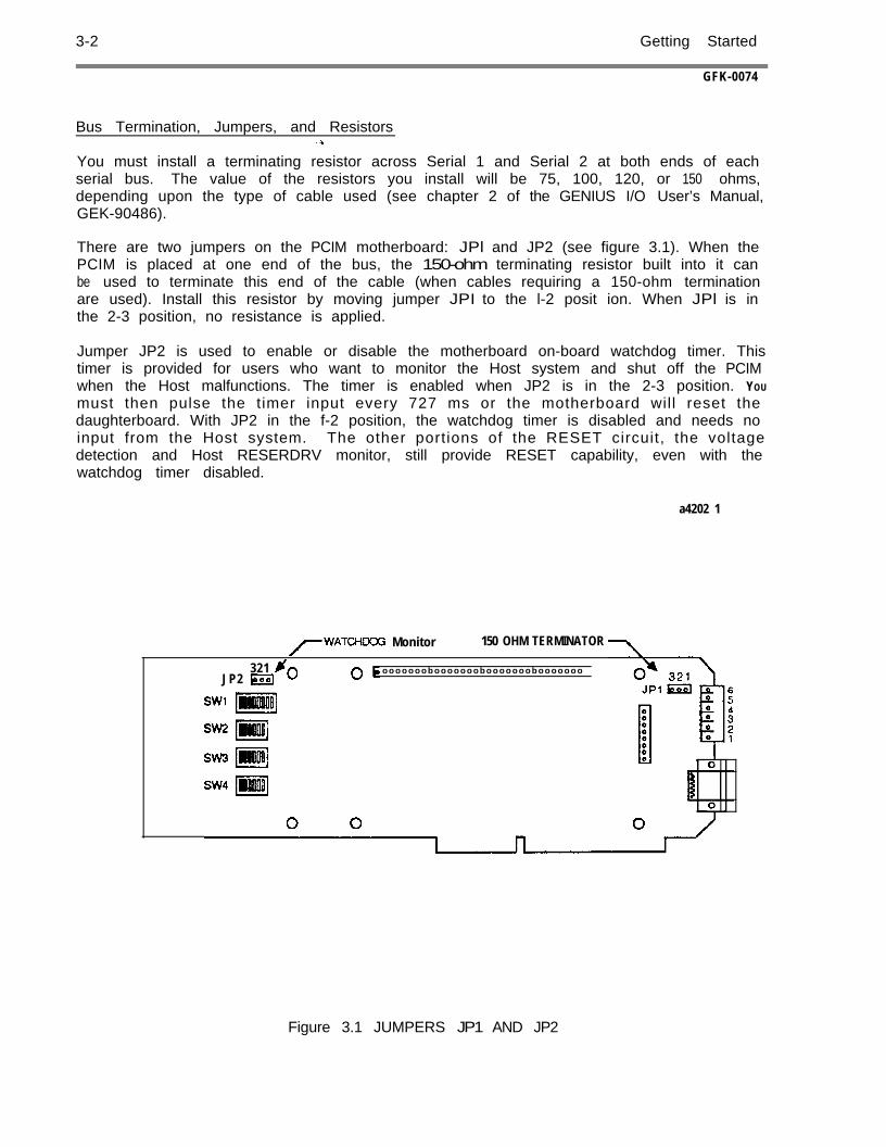
Bus Termination, Jumpers, and Resistors
You must install a terminating resistor across Serial 1 and Serial 2 at both ends of eachserial bus. The value of the resistors you install will be 75, 100, 120, or 150 ohms,depending upon the type of cable used (see chapter 2 of the GENIUS I/O User’s Manual,GEK-90486).
There are two jumpers on the PCIM motherboard: JPl and JP2 (see figure 3.1). When thePCIM is placed at one end of the bus, the 150-ohm terminating resistor built into it canbe used to terminate this end of the cable (when cables requiring a 150-ohm terminationare used). Install this resistor by moving jumper JPI to the l-2 posit ion. When JPl is inthe 2-3 position, no resistance is applied.
Jumper JP2 is used to enable or disable the motherboard on-board watchdog timer. Thistimer is provided for users who want to monitor the Host system and shut off the PCIMwhen the Host malfunctions. The timer is enabled when JP2 is in the 2-3 position. YOU
must then pulse the timer input every 727 ms or the motherboard will reset thedaughterboard. With JP2 in the f-2 position, the watchdog timer is disabled and needs noinput from the Host system. The other portions of the RESET circuit, the voltagedetection and Host RESERDRV monitor, still provide RESET capability, even with thewatchdog timer disabled.
a4202 1
/-WATCHOOG Monitor 150 OHM TERMINATOR
321 NJP2 &I o Ob ooooooobooooooobooooooobooooooo
Figure 3.1 JUMPERS JP1 AND JP2
Getting Started 3-3
GFK-0074
ADDRESSING
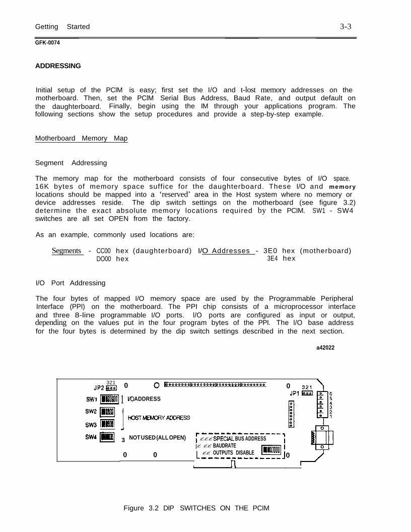
Initial setup of the PClM is easy; first set the I/O and t-lost memory addresses on themotherboard. Then, set the PClM Serial Bus Address, Baud Rate, and output default onthe daughterboard. Finally, begin using the IM through your applications program. Thefollowing sections show the setup procedures and provide a step-by-step example.
Motherboard Memory Map
Segment Addressing
The memory map for the motherboard consists of four consecutive bytes of I/O space.16K bytes of memory space suffice for the daughterboard. These I/O and memorylocations should be mapped into a ‘reserved’ area in the Host system where no memory ordevice addresses reside. The dip switch settings on the motherboard (see figure 3.2)determine the exact absolute memory locations required by the PCIM. SW1 - SW4switches are all set OPEN from the factory.
As an example, commonly used locations are:
Segments - CC00 hex (daughterboard) I/O Addresses - 3E0 hex (motherboard)DO00 hex 3E4 hex
I/O Port Addressing
The four bytes of mapped I/O memory space are used by the Programmable PeripheralInterface (PPI) on the motherboard. The PPI chip consists of a microprocessor interfaceand three 8-line programmable I/O ports. l/O ports are configured as input or output,depending on the values put in the four program bytes of the PPI. The l/O base addressfor the four bytes is determined by the dip switch settings described in the next section.
a42022
321JPZ m
SW1 pimiq
SW2
SW3 ImiBl
SW4 pq
0 OOOOQOO~OOOOOOO~OOOOOOO~OQQOOOO
1 VO ADDRESS
1 HOSThhEtKRY ADDH3S
A
3-1------------
NOT USED (ALL OPEN) ????SPECLAL BUS ADDRESS?? ?? BAUDRATE
;
0 0 L ?? OUTPUTS DISABLE----------m-w-
i-l
0JPl
0
:il00x00
Figure 3.2 DIP SWITCHES ON THE PCIM

3-4 Getting Started
GFK-0074
Motherboard Dip Switch Settings
SW1 - I/O Base Starting Address
The PPI-occupied 4 bytes of I/O space in the Host system is determined by the settings ofdip switch SW1. The starting address of the 4 byte I/O space is calculated as follows:
Dip Switch SW1position
- ->I2345678I I I I I I I I
--> A0 Al A2 A3 A4 A5 A6 A7 A8 A9
H o s t +-’ ‘-+‘T’address 3rd 2 n d 1st
bus d i g i t d i g i t digit (notice that address is reversed)
The i/O addresses available for the motherboard must begin on 4 byte boundaries. Thatis, the third digit of the I/O address must end in a ‘O’, ‘4’, ‘8’, or ‘C’ (hex). Therefore, thestarting addresses of the 4 byte I/O space range from 0 to 3FC (hex). To determine theswitch settings for a particular address, first establish the starting address of the 4 byteI/O space in l/O memory that the motherboard should use. Convert this address value tobinary and from the figure above, set OPEN the switches on SW1 corresponding to the ‘1’values in the binary value.
Example:
TO set dip switch SW1 for l/O address 3E0 (hex), first convert 3E0 to binary,which is
A0Al AZA3A4A5 A6A7A8A9I I Illf IIll0 0 0 0 0 1 1 1 1 1
‘--I--~ ‘-I-/ \?I0 E 3
for every occurrence of a 1, set the corresponding dip switch position of SW1OPEN as follows:
A2 A3 A4 A5 A6 A7 A8 A91 I I I I I I I0 0 0 1 1 1 1 1I I I I I I I I
Getting Started 3 - 5
GFK-0074
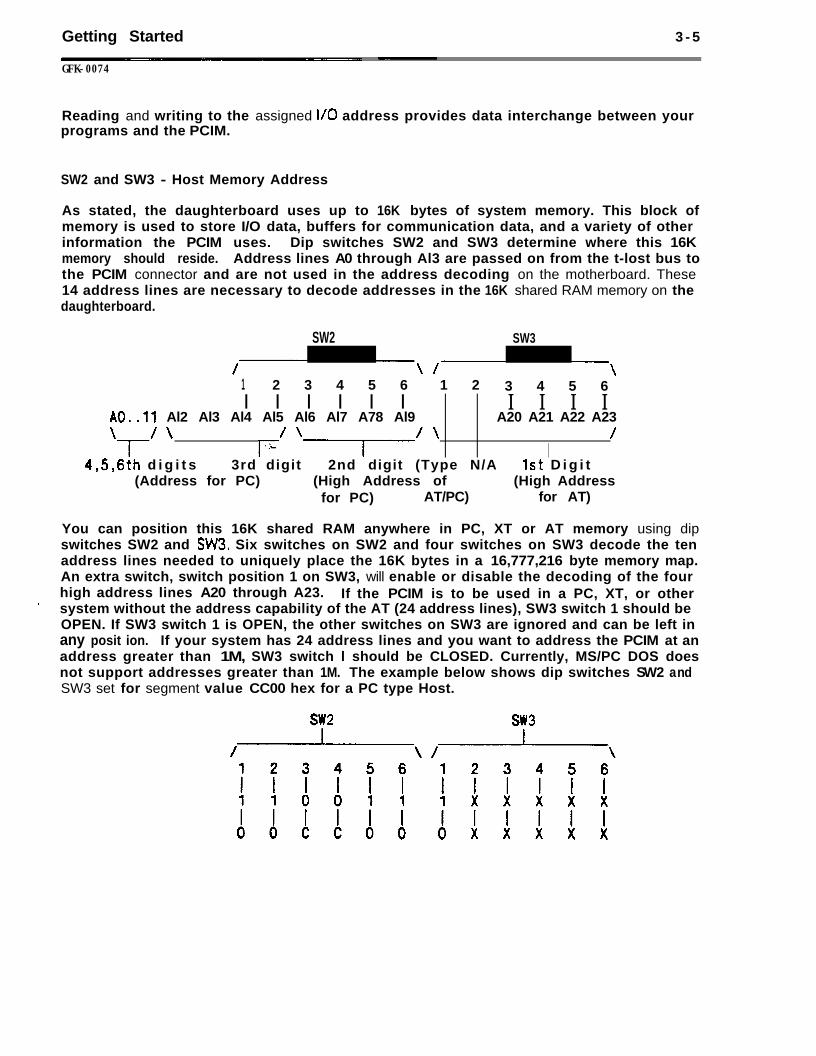
Reading and writing to the assigned I/O address provides data interchange between yourprograms and the PCIM.
SW2 and SW3 - Host Memory Address
As stated, the daughterboard uses up to 16K bytes of system memory. This block ofmemory is used to store I/O data, buffers for communication data, and a variety of otherinformation the PCIM uses. Dip switches SW2 and SW3 determine where this 16Kmemory should reside. Address lines A0 through Al3 are passed on from the t-lost bus tothe PCIM connector and are not used in the address decoding on the motherboard. These14 address lines are necessary to decode addresses in the 16K shared RAM memory on thedaughterboard.
SW2 SW3
/ \/ \1 2 3 4 5 6 1 2 3 4 5 6I I I I I I I I I I
AO..ll Al2 Al3 Al4 Al5 Al6 Al7 A78 Al9 A20 A21 A22 A23\ /\ /T-
I;/ ‘7’ ’ I4,5,6th d i g i t s 3rd digit 2nd digit (Type N/A
(Address for PC) (High Address of1st D i g i t
(High Addressfor PC) AT/PC) for AT)
You can position this 16K shared RAM anywhere in PC, XT or AT memory using dipswitches SW2 and SW3. Six switches on SW2 and four switches on SW3 decode the tenaddress lines needed to uniquely place the 16K bytes in a 16,777,216 byte memory map.An extra switch, switch position 1 on SW3, will enable or disable the decoding of the fourhigh address lines A20 through A23. If the PCIM is to be used in a PC, XT, or other
- system without the address capability of the AT (24 address lines), SW3 switch 1 should beOPEN. If SW3 switch 1 is OPEN, the other switches on SW3 are ignored and can be left inany posit ion. If your system has 24 address lines and you want to address the PCIM at anaddress greater than 1M, SW3 switch l should be CLOSED. Currently, MS/PC DOS doesnot support addresses greater than 1M. The example below shows dip switches SW2 andSW3 set for segment value CC00 hex for a PC type Host.
3-6 Getting Started
GFK-0074
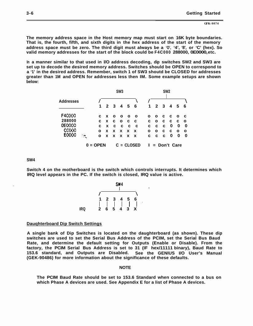
The memory address space in the Host memory map must start on 16K byte boundaries.That is, the fourth, fifth, and sixth digits in the hex address of the start of the memoryaddress space must be zero. The third digit must always be a ‘O’, ‘4’, ‘8’, or ‘C’ (hex). Sovalid memory addresses for the start of the block could be F4C000 288000, 0E0000, etc.
In a manner similar to that used in l/O address decoding, dip switches SW2 and SW3 areset up to decode the desired memory address. Switches should be OPEN to correspond toa ‘1’ in the desired address. Remember, switch 1 of SW3 shoutd be CLOSED for addressesgreater than 1M and OPEN for addresses less then IM. Some example setups are shownbelow:
SW3
Addresses / \1 2 3 4 5 6
f-4cooo c x o o o o288000 c x c o c cOEOOOO c x c c c c
cc000 o x x x x xEOOOO ‘+b o x x x x x
0 = OPEN C = CLOSED
SW4
SW2I
/ \1 2 3 4 5 6
o o c c o cc o c c c oc c c 0 0 0o o c c o oc c c 0 0 0
X = Don’t Care
Switch 4 on the motherboard is the switch which controls interrupts. It determines whichIRQ level appears in the PC. If the switch is closed, IRQ value is active.
/ \1 2 3 4 5 6I I I I II’
IRQ 2 6 5 4 3 X
Dauqhterboard Dip Switch Settings
A single bank of Dip Switches is located on the daughterboard (as shown). These dipswitches are used to set the Serial Bus Address of the PCIM, set the Serial Bus BaudRate, and determine the default setting for Outputs (Enable or Disable). From thefactory, the PCIM Serial Bus Address is set to 31 (IF hex/11111 binary), Baud Rate to153.6 standard, and Outputs are Disabled. See the GENIUS I/O User’s Manual(GEK-90486) for more information about the significance of these defaults.
NOTE
The PCIM Baud Rate should be set to 153.6 Standard when connected to a bus onwhich Phase A devices are used. See Appendix E for a list of Phase A devices.
Getting Started 3-7
GFK-0074
yyy?zz Bus Addressi---i----------------S e r i a l B u s B a u d R a t e
0 0 - 153.6 Extended (8 bit skip time)01 - 38.4 (8 bit skip time)10 - 76.8 (8 bit skip time)11 - 153.6 Standard (4 bit skip time)
t------------------------ Default Output Disable0 - Outputs Enabled1 - Outputs Disabled
The four bytes of mapped I/O memory space are used by the Programmable PeripheralInterface (PPI) on the motherboard. The PPI chip consists of a microprocessor interfaceand three 8-line programmable I/O ports. These four bytes start at the l/O base addressdetermined by the switch settings on SW1 and are in sequence as shown below. The fourPPI I/O bytes then, are Port A Data, Port B Data, Port C Data and the Control Byte. I/Oports are configured as input or output, depending on the values put in the four programbytes of the PPI, which are as follows:
Byte # A 8 - A0 Description/ \
0 xxxxxxxoo Port A Data byte1 xxxxxxxo 1 Port B Data byte2 xxxxxxx10 Port C Data byte3 xxxxxxx 11 Control byte
For example, if the switches on SW1 are set for 3E0 (hex), you can perform I/O operationson the four PPI bytes at addresses:
(3E0 t 0) = 3E0 Port A Data Byte (PCIM Status)(3E0 t 1) = 3E1 P o r t 5 D a t a B y t e (PCIM C o n t r o l )(3E0 + 2) = 3E2 P o r t C D a t a B y t e ( n o t u s e d )(3E0 t 3 ) = 3E3 C o n t r o l B y t e
Port A, B and C bytes are read/write, whereas the Control byte is write-only.
On the motherboard, Port A of the PPI is used as in input port, Port B as an output portand Port C is not connected. When Port A is programmed as an input port, all eight lineswill present high impedance load to the rest of the circuit. Port B, on the other hand,when programmed as an output port will look like all high (logic 1) outputs when it is firstprogrammed as an output port. Therefore, you should lower some of the lines in Port B totheir ‘default’ positions as outlined in the following descriptions.
3-8 Getting Started
GFK-0074
The functions for each pin of tbe PPI are as follows;
- Port A:
0 - low voltage/Host RESET detect
This input monitors the output of a bi-stable latch controlled by thevoltage detection circuit and the Host system RESETDRV line. Itgoes low and stays low (until reset) whenever the voltage on themotherboard drops below 3.12 volts or the system RESETDRV linegoes high, indicating the Host system has gone into RESET. Thelatch controlling this line is reset by the ‘1’ bit of Port B. Duringnormal operation this line should stay high (logic 1).
1 - watchdog timer status
This line is high while the watchdog timer is enabled (by jumperJP2) and being pulsed every 727 ms by output 0 of Port B. If thetimer times out, this line goes low (logic 0). It will go low if eitherthe voltage detector detects a low voltage or the systemRESETDRV line goes high and the timer times out. The timer willtime out if not pulsed every 727 ms (with jumper JP2 in the2-3/Enabled posit ion).
2 - interrupt request
When the daughterboard generates an interrupt to the motherboard,this line goes high (logic 1) and stays high until reset by output 2 ofPort B. The bi-stable latch that stores this interrupt is edgetriggered.
3 - PClM OK signal
The state of this line follows the condition of the PClM OK LED onthe daughterboard. If the LED is lit, the PClM OK signal into thePPI is low (logic 0).
4 - COMM (communications) OK signal
Like the BOARD OK signal above, this signal also follows theoutput of one of the LEDs on the daughterboard. This line into thePPI is low (logic 0) if the COMM OK LED on the daughterboard isl it.
5 - NC
6 - N C
7 - N C
Getting Star-ted 3-9
- Port B:
0 - watchdog timer pulse signal
If the watchdog timer is enabled by jumper JP22, this line should bepulsed at least every 727 ms in order to keep the watchdog timertiming. The timer is triggered on the rising edge of the signal, so itis necessary for you to program the PPI to provide a low to hightransition on this signal line. This line must be pulsed at least onceto allow the daughterboard to come out of RESET.
1 - clear RESET request
When the system RESETDRV signal goes high indicating a systemRESET, or when the voltage detector on the motherboard detects aIow voltage condition, a bi-stable latch is set that drives themotherboard RESET circuit. The output of this latch can be readon bit 0 of Port A on the PPI (see above). This line (bit 1 of Port B)clears the latch when lowered (logic O), and when raised again (logic1), readies the latch for the next detection of RESET or low voltagecondition.
2 - clear interrupt request
This line is used to clear the interrupt request bi-stable latch on themotherboard after an interrupt has been received from thedaughterboard. Bringing the line logic 0 clears the latch and thenback to logic 1 prepares it for the next interrupt. As long as thisline is low, the latch will not latch incoming interrupt requests.
3 - HHM test
An HHM present can be indicated even when one isn’t plugged in byraising this line to a logic 1. After power up and under normalconditions, lower (logic 0) this line and leave it low.
4 - factory test
This line should not be used and should be left low (logic 0) all thetime.
5 - interrupt output (to the daughterboard)
This output from Port B drives the GENINT/ interrupt line to thePCIM connector. When pulsed low (logic 0) it requests an interruptfrom the daughterboard. Not operational for the PCIM - should belogic 0.
6 - PCIM RESET
When this line is low (logic 0) it pulls the PCIM into RESET. Undernormal conditions, it should be left high.
7-NC

3-l 0 Getting Started
GFK-0074
Application Example
To set up the PCIM, first set up the PPI. The PPI is initialized by defining ports A and Cas input ports and port B as an output port.
In BASIC, this statement would suffice:
100 OUT 959,153
This example statement writes a value of 153 decimal (99 hex) to the control byte of thePPI located in I/O memory at location 995 decimal, or 3E0 hex. For the purposes of thisexample, assume the dip switches have been set to respond to the I/O address range of992 hex through 995 hex. The value of 99 hex causes ports A and C to be configured asinputs and port B as an output port. Port B is now an output port and all eight of itsoutputs are high - they shouldn’t be left that way for long. Lines D1, D2, D3, D6 and D7of port B should be lowered to prevent any interrupts to the Host system and make surethe PCIM is in RESET, always a good place to start. The BASIC statement to performthis is:
110 OUT 993,01
This statement writes a 1 decimal (1 hex) value to Port B byte. Then, to bring the PClMout of RESET, execute the following statement:
120 OUT 993,67
This raises D1 and D6, and allows the PCIM daughterboard to run in the memory spacedetermined by the dip switch settings.
That is:
nnn OUT Base t 3, 99hnnn OUT Base t 1, lnnn OUT Base t 1, 43h
In Microsoft C compiler, the library function ‘outp (port, value)’ is used,
Try coding the values shown in the Basic example above in the following in Microsoft Cstatements to set ON the PCIM:
outp ((BASE + 3), 0 x 99);outp ((BASE + 1), 1);outp ((BASE + 1), 0 x 43);
Getting Started 3-11
GFK-0074
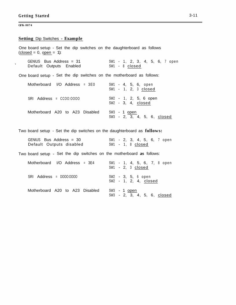
Setting Dip Switches - Example
One board setup - Set the dip switches on the daughterboard as follows(closed = 0, open = 1):
GENIUS Bus Address = 31 SW1 - 1 , 2, 3, 4, 5, 6, 7 o p e n5Default Outputs Enabled SW1 - 8 closed
One board setup - Set the dip switches on the motherboard as follows:
Motherboard l/O Address = 3E0 SW1 - 4, 5, 6, o p e nSW1 - 1 , 2, 3 closed
SRI Address = CCOO:OOOO SW2 - 1 , 2, 5, 6 openSW2 - 3, 4, closed
Motherboard A20 to A23 Disabled SW3 - 1 openSW3 - 2, 3, 4, 5, 6, closed
Two board setup - Set the dip switches on the daughterboard as follows:
GENIUS Bus Address = 30Default Outputs disabled
SW1 - 2, 3, 4, 5, 6, 7 o p e nSW1 - 1 , 8 closed
Two board setup - Set the dip switches on the motherboard as follows:
Motherboard I/O Address = 3E4 SW1 - 1 , 4, 5, 6, 7, 8 o p e nSW1 - 2, 3 closed
SRI Address = DOOO:OOOO SW2 - 3, 5, 6 o p e nSW2 - 1 , 2, 4, closed
Motherboard A20 to A23 Disabled SW3 - 1 openSW3 - 2, 3, 4, 5, 6, closed
3-l 2 Getting Started
GFK-0074
Communications Cable
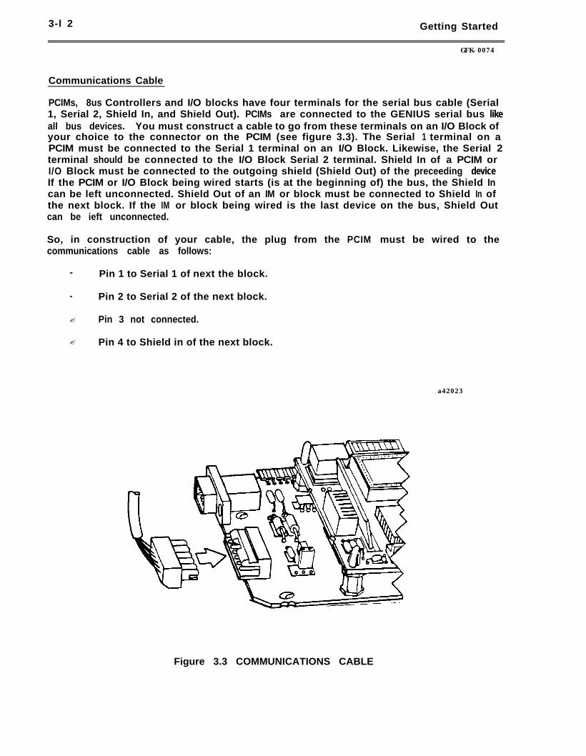
PCIMs, 8us Controllers and I/O blocks have four terminals for the serial bus cable (Serial1, Serial 2, Shield In, and Shield Out). PCIMs are connected to the GENIUS serial bus likeall bus devices. You must construct a cable to go from these terminals on an I/O Block ofyour choice to the connector on the PCIM (see figure 3.3). The Serial 1 terminal on aPCIM must be connected to the Serial 1 terminal on an I/O Block. Likewise, the Serial 2terminal should be connected to the I/O Block Serial 2 terminal. Shield In of a PCIM orI/O Block must be connected to the outgoing shield (Shield Out) of the preceeding deviceIf the PCIM or I/O Block being wired starts (is at the beginning of) the bus, the Shield Incan be left unconnected. Shield Out of an IM or block must be connected to Shield In ofthe next block. If the IM or block being wired is the last device on the bus, Shield Outcan be ieft unconnected.
So, in construction of your cable, the plug from the PCIM must be wired to thecommunications cable as follows:
- Pin 1 to Serial 1 of next the block.
- Pin 2 to Serial 2 of the next block.
? Pin 3 not connected.
? Pin 4 to Shield in of the next block.
a42023
Figure 3.3 COMMUNICATIONS CABLE

Getting Started 3-13
GFK-0074
a42024
Side View
Figure 3.4 PCIM INSTALLATION
PCIM lnstal lation
1) Power OFF the Host computer and unplug from power source.
2 ) Plug the PClM into any available slot (remember, space for two slots is required foran IBM PC AT, XT, or Workmastershown above.
- CIMSTAR I requires only one) in the Host asMake sure the edge connectors are firmly seated, and the mounting
bracket aligned. Then, tighten the mounting screw.
DO NOT
- Mount the PCIM where air flow across it is obstructed
- Mount the PCIM nearer than 1/8” (.125”) to any other boards or rackcomponents
- Use adhesives or conformal coatings on any part of the PCIM
3) Connect one end of the communications cable you made to designated I/O Block onthe serial bus, and the other end to the PCIM installed in the Host.
4) For board installation information for specific Hosts, refer to OEM user’s manuals,such as IBM’s “Guide to Operations”.
3-14 Getting Started
G F K - 0 0 7 4
PCIM startup
You may now activate the PCIM as follows:
1)
2)
3)
4)
Plug in and power ON the Host computer.
- The PCIM performs self tests verifying that processor, RAM, timers and theI ike are operational. If both LEDs are set ON, power up was successful.
Insert an MS DOS 3.0 (or higher) software disk into Drive A.
Insert the provided diskette containing the Software Driver and associated files intoDrive B.
After MS DOS boots, set the active disk drive to ‘B’.
- Beyond the self tests, the PCIM will do nothing until it is explicitly taken outof RESET. This is accomplished via the application program code you write -specifically, through the INlTlM Software Driver function call explained inchapter 4.
- Before the Software Driver can be used, function call subroutines must first beloaded into your system. Further, each Basic program accessing the Drivermust perform a short startup sequence. The details of these operations followin chapter 4.
Getting Started
GFK-0074
3-15
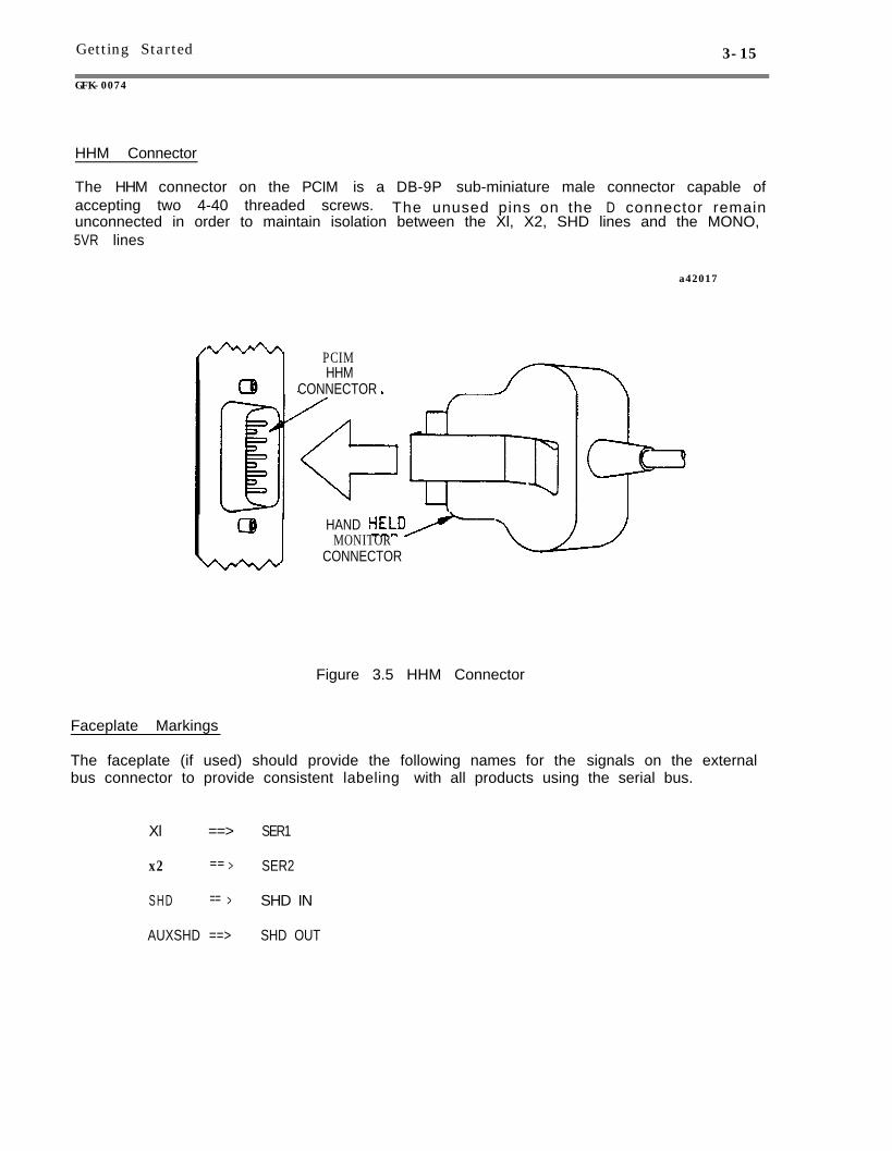
HHM Connector
The HHM connector on the PCIM is a DB-9P sub-miniature male connector capable ofaccepting two 4-40 threaded screws. The unused pins on the D connector remainunconnected in order to maintain isolation between the Xl, X2, SHD lines and the MONO,5VR lines
a42017
/ PCIMHHM
CONNECTOR
HAND HELD,,+--MONITOR
CONNECTOR
Figure 3.5 HHM Connector
Faceplate Markings
The faceplate (if used) should provide the following names for the signals on the externalbus connector to provide consistent labeling with all products using the serial bus.
Xl ==> SER1
x2 == > SER2
S H D == > SHD IN
AUXSHD ==> SHD OUT

PCIM Software Driver 4 - l
GFK-0074
CHAPTER 4PCIM SOFTWARE DRIVER
INTRODUCTION
This chapter outlines the functionality of the PCIM Software Driver, which provides ahigh level interface between applications software you develop and the PCIM; andthrough the PCIM, devices on the GENIUS serial bus. The PCIM Software Driver isaccessed through a set of subroutine calls. The PCIM Software Driver is compatible withapplications software custom designed by your OEM, or prepackaged software such asCIMPAC.
Languages
The PCIM Software Driver is provided in versions compatible with C language and Basiclanguage, specified as a set of function calls in order to allow a consistent interface withboth languages. Driver software is delivered in the form of object code in a single.exe/(.COM) f i l e . It'ss guide covers both C language and Basic languageapplications.
Host Operating System
The PCIM Software Driver is supplied in a version compatible the MSDOS operatingsystem, as follows:
1) C/MSDOS
2) BASIC/MSDOS
Software Driver Function Calls
The PCIM Software Driver consists of easy to use macro-oriented function calls you codeappropriately in your C language or Basic language applications routines. Function callsare summarized below.
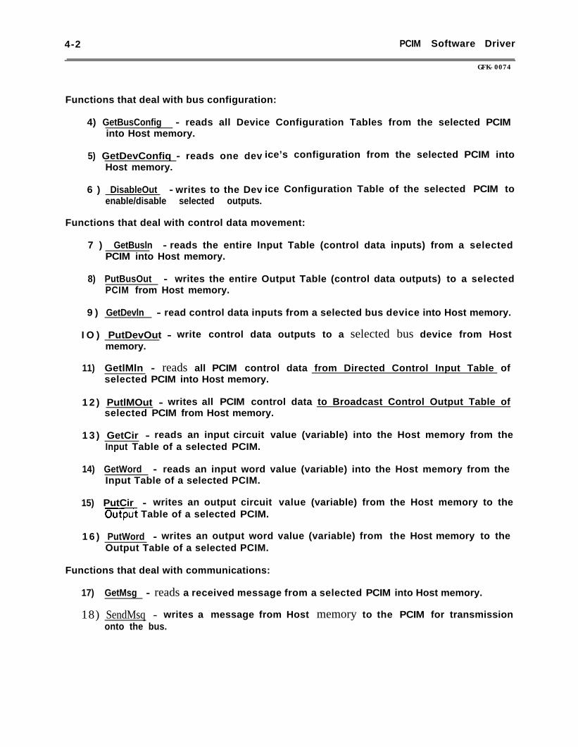
Functions that deal with PCIM configuration:
1 ) InitlM - assigns PCIM numbers and Global data parameters to all PCIMs.Performs any required hardware activation and initialization of the PCIMs (suchas Reset).
2 ) ChqlMSetup - writes to the Setup Table of the selected PCIM frommemory to change PCIM parameters.
3) GetlMState - reads PClM configuration and status from the selected PCIMTable and Setup Table into Host memory.
the Host
Status
4-2 PCIM Software Driver
GFK-0074
Functions that deal with bus configuration:
4) GetBusConfig - reads all Device Configuration Tables from the selected PCIMinto Host memory.
5) GetDevConfiq - reads one devHost memory.
6 ) DisableOut - writes to the Devenable/disable selected outputs.
ice’s configuration from the selected PCIM into
ice Configuration Table of the selected PCIM to
Functions that deal with control data movement:
7 ) GetBusln - reads the entire Input Table (control data inputs) from a selectedPCIM into Host memory.
8) PutBusOut - writes the entire Output Table (control data outputs) to a selectedPCIM from Host memory.
9 ) GetDevln - read control data inputs from a selected bus device into Host memory.
I O ) PutDevOut - write control data outputs to a selected bus device from Hostmemory.
11) GetlMln - reads all PCIM control data from Directed Control Input Table ofselected PCIM into Host memory.
1 2 ) PutlMOut - writes all PCIM control data to Broadcast Control Output Table ofselected PCIM from Host memory.
1 3 ) GetCir - reads an input circuit value (variable) into the Host memory from theInput Table of a selected PCIM.
14) GetWord - reads an input word value (variable) into the Host memory from theInput Table of a selected PCIM.
15) PutCir - writes an output circuit value (variable) from the Host memory to them Table of a selected PCIM.
1 6 ) PutWord - writes an output word value (variable) from the Host memory to theOutput Table of a selected PCIM.
Functions that deal with communications:
17) GetMsg - reads a received message from a selected PCIM into Host memory.
18) SendMsq - writes a message from Host memory to the PCIM for transmissiononto the bus.

PCIM Software Driver9GM-0074
4-3
Functions that deal with communications (Cont’d):
19) SendMsqReply - writes a message from Host memory to the PCIM fortransmission onto the bus and expects a specified reply message from thedestination.
20) ChkMsqStat - allows the Host to detect when a transmitted message has actuallybeen completed, or if transmission is incomplete or has failed.
Functions that deal with interrupt processing:
21) - - reads the entire interrupt Status Table from a selected bus device intoHost memory.
22) PutlNTR - writes the entire Interrupt Status Table to a selected PCIM from Hostmemory.
Using Software Driver Function Calls
When coding the PCIM Software Drivers in your application programs, you should have athand the following:
8 Starting Address (Segment Address) of the SRI.
.* l/O Port Ease Address.
8 Status Table Address (PCIMs) or Reference Address (Series Six).
0 Serial Bus Address of each bus device.
0 Global, Input, Output Data lengths.
I SW1 - SW5 Dipsw i tch values.
8 GENIUS I/O Bus Datagram Services (GFK-0090)
It is also helpful to have the GENIUS t/O Manual (GEK-XM86) and the Series SixInterface to the Genius I/O System Manual (GFK-0171) handy for reference.
This Chapter Has Two Sections
If your application is coded in C language, go on to Section A. tf you are using BASIC,notation and coding conventions for your application are described in section B.

PCIM C Software Driver
CFK-0074
SECTION AC LANGUAGE PCIM SOFTWARE DRIVER
C SOFTWARE DRIVER INSTALLATION
Compiling your Application with Microsoft
In order to make your C application compatible with the PCIM library, you must firstinvoke the Microsoft compiler with the following switch (option):
/Zp
This option permits user-packed data structures and is required for the GetlMState,GetlBusConf ig, and GetDevConf ig calls. For example:
C> msc application /Zp; (small model)
OR
C> msc application /Zp/AL; (large model)
Software File Linkage
It is necessary to link and load the file named SPCIMLIB” (small model) or LPCIM.LIBVf(large model) before using the C Software Drivers in your programs. There are severalways to link the PCIM.LIB using the Microsoft Linker,
1) The simplest way is to type all of the necessary module information on the commandline:
‘LINK PROGRAM+MODULE,,,\SEARCH\PATH\SPClM.LIB;’ (small model)
OR
‘LINK PROGRAM+MODULE,,,\SEARCH\PATH\LPCIM.LIB;’ (large model)
2) However, if the program is divided up into several modules too numerous to fit onthe command line, you can set up a response file to tink all of the associated objectfiles. The contents of a response file might look like:
program+modulel +modute2+module3+moduIe4+....+moduleN,program.exe,program.map,\search\path\pcim.lib
The command to fink the response file is:
LINK @RESPONSE.FIL
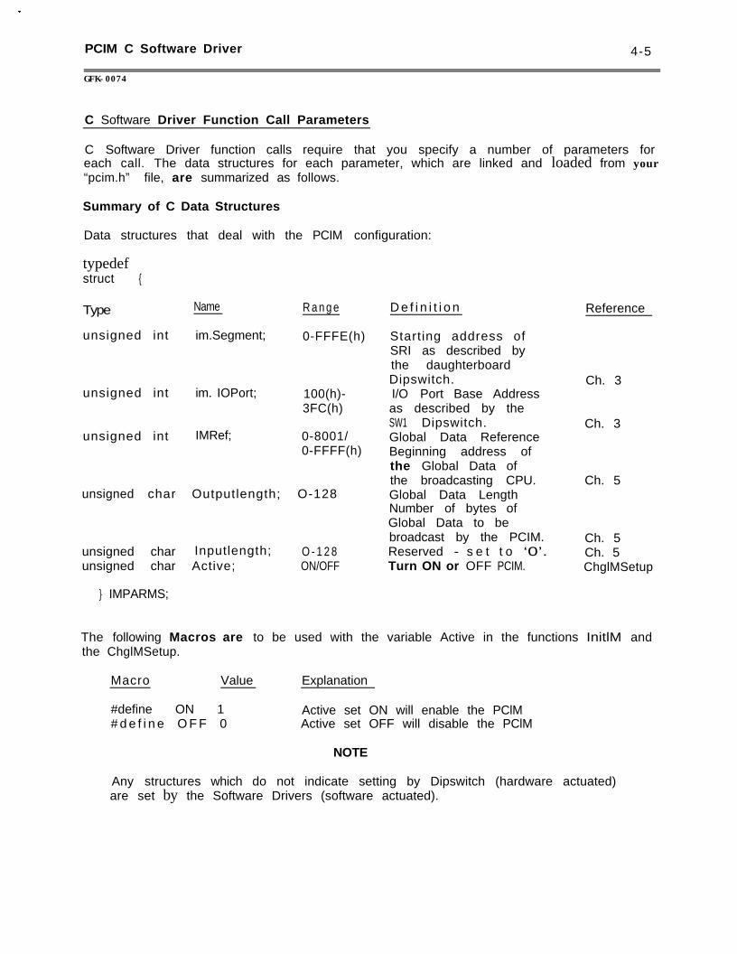
PCIM C Software Driver 4-5
GFK-0074
C Software Driver Function Call Parameters
C Software Driver function calls require that you specify a number of parameters foreach call. The data structures for each parameter, which are linked and loaded from your“pcim.h” file, are summarized as follows.
Summary of C Data Structures
Data structures that deal with the PCIM configuration:
typedefstruct {
Type Name R a n g e
unsigned int im.Segment; 0-FFFE(h)
unsigned int im. IOPort; 100(h)-3FC(h)
unsigned int IMRef; 0-8001/0-FFFF(h)
unsigned char Outputlength; O-128
unsigned char Inputlength; O - 1 2 8unsigned char Active; ON/OFF
} IMPARMS;
D e f i n i t i o n
Starting address ofSRI as described bythe daughterboardDipswitch.I/O Port Base Addressas described by theSW1 Dipswitch.Global Data ReferenceBeginning address ofthe Global Data ofthe broadcasting CPU.Global Data LengthNumber of bytes ofGlobal Data to bebroadcast by the PCIM.Reserved - s e t t o ‘0’.Turn ON or OFF PCIM.
Reference
Ch. 3
Ch. 3
Ch. 5
Ch. 5Ch. 5ChglMSetup
The following Macros are to be used with the variable Active in the functions InitlM andthe ChglMSetup.
Macro Value Explanation
#define ON 1# d e f i n e O F F 0
Active set ON will enable the PClMActive set OFF will disable the PClM
NOTE
Any structures which do not indicate setting by Dipswitch (hardware actuated)are set by the Software Drivers (software actuated).
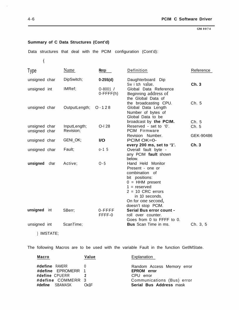
?
4-6 PCIM C Software Driver
GM-0074
Summary of C Data Structures (Cont’d)
Data structures that deal with the PCIM configuration (Cont’d):
Typeunsigned char
unsigned int
unsigned char
unsigned charunsigned char
unsigned char
unsigned char
unsigned char
unsigned int SBerr;
unsigned int ScanTime;
Name
DipSwitch;
IMRef;
RanqeR
0-255(d)
O-8001 /0-FFFF(h)
OutputLength; O - 1 2 8
InputLength;Revision;
GENI_OK;
Fault;
O-l 28
l/O
o-1 5
Active; O - 5
0-FFFFFFFF-0
Definition
Daughterboard DipSW i tch value.Global Data ReferenceBeginning address ofthe Global Data ofthe broadcasting CPU.Global Data LengthNumber of bytes ofGlobal Data to bebroadcast by the PCIM.Reserved - set to ‘0’.PCIM FirmwareRevision Number.PClM OK=0-every 200 ms, set to ‘1’.Overall fault byte -any PCIM fault shownbelow.Hand Held MonitorPresent - one orcombination ofbit positions:0 = HHM present1 = reserved2 = 10 CRC errors
in 10 seconds.On for one second,doesn’t stop PCIM.Serial Bus error count -roll over counter.Goes from 0 to FFFF to 0.Bus Scan Time in ms.
Reference
Ch. 3
Ch. 5
Ch. 5Ch. 5
GEK-90486
Ch. 3
Ch. 3, 5
} IMSTATE;
The following Macros are to be used with the variable Fault in the function GetlMState.
Macro Value
#define RAMERR 0#define EPROMERR 1#define CPUERR 2#def ine COMMERR 3#define SBAMASK Ox1F
Explanation
Random Access Memory errorEPROM errorCPU errorCommunications (Bus) errorSerial Bus Address mask
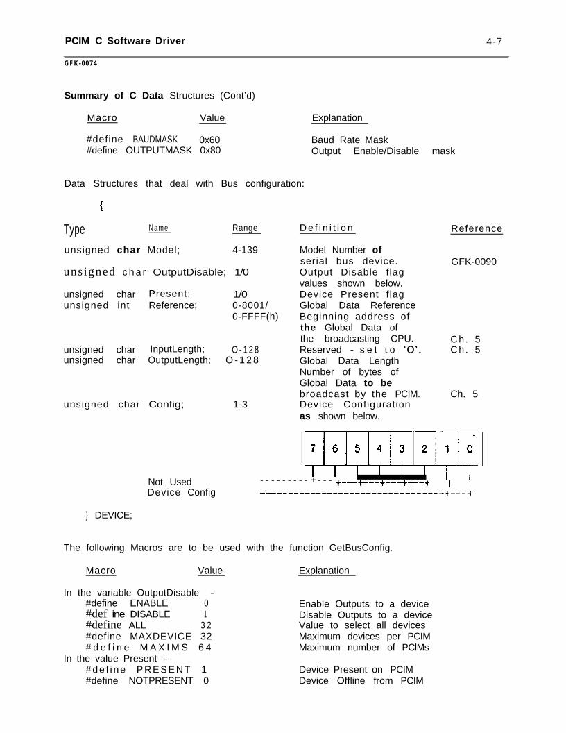
PCIM C Software Driver 4-7
G F K - 0 0 7 4
Summary of C Data Structures (Cont’d)
Macro Value Explanation
#define BAUDMASK 0x60 Baud Rate Mask#define OUTPUTMASK 0x80 Output Enable/Disable mask
Data Structures that deal with Bus configuration:
Type Name Range
unsigned char Model; 4-139
unsigned c h a r OutputDisable; 1/0
unsigned char Present; 1/0unsigned int Reference; 0-8001/
0-FFFF(h)
unsigned char InputLength; O - 1 2 8unsigned char OutputLength; O - 1 2 8
unsigned char Config; 1-3
D e f i n i t i o n Reference
Model Number ofserial bus device. GFK-0090Output Disable flagvalues shown below.Device Present flagGlobal Data ReferenceBeginning address ofthe Global Data ofthe broadcasting CPU. Ch . 5Reserved - s e t t o ‘0’. Ch . 5Global Data LengthNumber of bytes ofGlobal Data to bebroadcast by the PCIM. Ch. 5Device Configurationas shown below.
Not Used - - - - - - - - - - - -+ +---t---+---+---t 1 1Device Config ---------------------------------t---+
} DEVICE;
The following Macros are to be used with the function GetBusConfig.
Macro Value
In the variable OutputDisable -#define ENABLE 0#def ine DISABLE 1#define ALL 3 2#define MAXDEVICE 32# d e f i n e M A X I M S 6 4
In the value Present -#de f i ne PRESENT 1#define NOTPRESENT 0
Explanation
Enable Outputs to a deviceDisable Outputs to a deviceValue to select all devicesMaximum devices per PCIMMaximum number of PClMs
Device Present on PCIMDevice Offline from PCIM
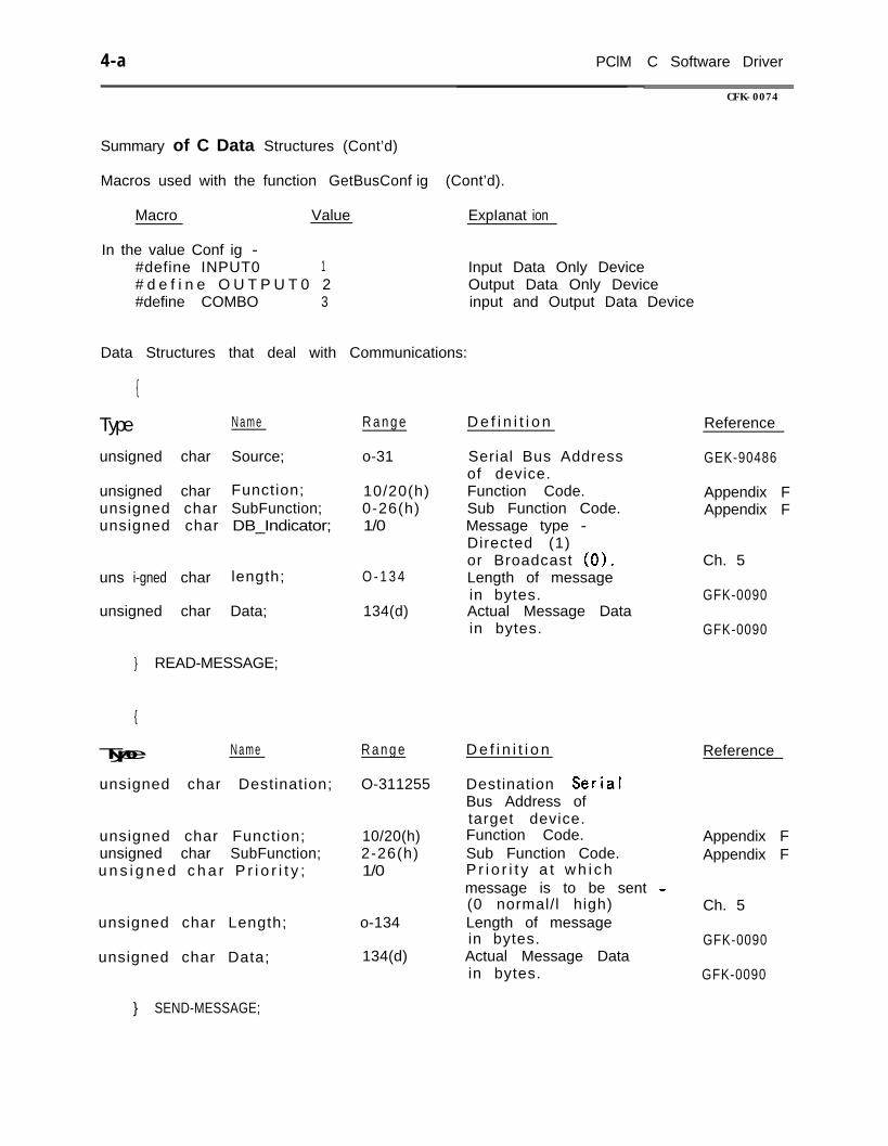
4-a PClM C Software Driver
CFK-0074
Summary of C Data Structures (Cont’d)
Macros used with the function GetBusConf ig (Cont’d).
Macro Value ExpIanat ion
In the value Conf ig -#define INPUT0 1# d e f i n e O U T P U T 0 2#define COMBO 3
Input Data Only DeviceOutput Data Only Deviceinput and Output Data Device
Data Structures that deal with Communications:
{
Type Name R a n g e
unsigned char Source; o-31
unsigned char Function; 10/20(h)unsigned char SubFunction; 0-26(h)unsigned char DB_Indicator; 1/0
uns i-gned char length;
unsigned char Data;
} READ-MESSAGE;
O - 1 3 4
134(d)
{
Type Name
unsigned char Destination;
R a n g e
O-311255
unsigned char Function; 10/20(h)unsigned char SubFunction; 2-26(h)u n s i g n e d c h a r P r i o r i t y ; 1/0
unsigned char Length;
unsigned char Data;
o-134
134(d)
} SEND-MESSAGE;
D e f i n i t i o n
Serial Bus Addressof device.Function Code.Sub Function Code.Message type -Directed (1)or Broadcast -Length of messagein bytes.Actual Message Datain bytes.
D e f i n i t i o n
Destination SerialBus Address oftarget device.Function Code.Sub Function Code.P r i o r i t y a t w h i c hmessage is to be sent(0 normal/l high)Length of messagein bytes.Actual Message Datain bytes.
Reference
GEK-90486
Appendix FAppendix F
Ch. 5
GFK-0090
GFK-0090
Reference
Appendix FAppendix F
Ch. 5
GFK-0090
GFK-0090

PCIM C Software Driver
UK-0074
Summary of C Data Structures (Cont’d)
Data Structures that deal with Communications (Cont’d):
Name Range
unsigned char Destination; o-31
unsigned char Function; 10/20(h)unsigned char TVSubFunction; 2-26(h)
uns i gned char R_SubFunction; 2-26(h)
unsigned char P r i o r i t y ; 1/0
unsigned char T-Length; o-134
unsigned char Data; .i 134(d)
_} SEND_MESSAGE_REPLY;
D e f i n i t i o n
Destination SerialBus Address oftarget device.Function Code.Sub Function Code -(transmitted).Sub function Code -(expected reply).P r i o r i t y a t wh ichmessage is to be sent -(0 normal/l high)length of messagein bytes.Actual Message Datain bytes.
Reference
GEK-90486Appendix F
Appendix F
Appendix F
Ch. 5
GFK-0090
GFK-0090
The following Macro is used by the Destination variable in the MESSAGE structures:
Macro Value Explanation
#def ine BROADCAST 255 M e s s a g e to b e s e n t a t B r o a d c a s tControl data priority.
T h e 1 Following Macros are used by the Priority variable in the MESSAGE structures.
Macro Value
# d e f i n e NORMALP 0#define HIGHP 1
Explanation
Message to be sent at normal priority.Message to be sent at high priority.
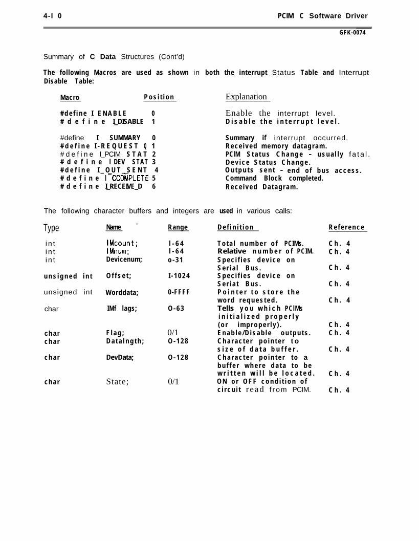
4-l 0 PClM C Software Driver
GFK-0074
Summary of C Data Structures (Cont’d)
The following Macros are used as shown in both the interrupt Status Table and InterruptDisable Table:
Macro P o s i t i o n
# d e f i n e I E N A B L E 0# d e f i n e I_DISABLE 1
#define I SUMMARY 0# d e f i n e I - R E Q U E S T Q 1# d e f i n e I_PCIM S T A T 2# d e f i n e l DEV STAT 3# d e f i n e I _ O U T _ S E N T 4# d e f i n e I CCOMPLETE 5# d e f i n e I_RECEIVE_D 6
Explanation
Enable the interrupt level.D i s a b l e t h e i n t e r r u p t l e v e l .
Summary if interrupt occurred.Rece ived memory da tagram.PClM S t a t u s C h a n g e - u s u a l l y f a t a l .D e v i c e S t a t u s C h a n g e .O u t p u t s s e n t - e n d o f b u s a c c e s s .Command Block completed.R e c e i v e d D a t a g r a m .
The following character buffers and integers are used in various calls:
Typei n ti n ti n t
u n s i g n e d i n t
unsigned int
char
charc h a r
c h a r
c h a r
Name.
Mount;IMnum;Devicenum;
O f f s e t ;
Worddata;
IMf lags;
F l a g ;D a t a l n g t h ;
DevData;
State;
Range
l - 6 4l - 6 4o - 3 1
I - 1 0 2 4
0-FFFF
O - 6 3
0/1O - 1 2 8
O - 1 2 8
0/1
D e f i n i t i o n
T o t a l n u m b e r o f PCIMs.Relative n u m b e r o f PCIM.S p e c i f i e s d e v i c e o nS e r i a l B u s .S p e c i f i e s d e v i c e o nS e r i a t B u s .P o i n t e r t o s t o r e t h ew o r d r e q u e s t e d .Tells y o u w h i c h PClMsi n i t i a l i z e d p r o p e r l y( o r i m p r o p e r l y ) .E n a b l e / D i s a b l e o u t p u t s .C h a r a c t e r p o i n t e r t os i z e o f d a t a b u f f e r .C h a r a c t e r p o i n t e r t o ab u f f e r w h e r e d a t a t o b ew r i t t e n w i l l b e l o c a t e d .O N o r O F F c o n d i t i o n o fc i r c u i t read f r o m PCIM.
R e f e r e n c e
C h . 4C h . 4
C h . 4
C h . 4
C h . 4
C h . 4C h . 4
C h . 4
C h . 4
C h . 4
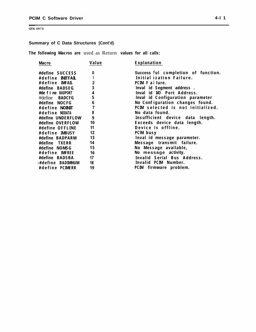
PCIM C Software Driver 4-l 1--..GFK-0074
Summary of C Data Structures (Cont’d)
The following Macros are used as Return values for all calls:
Macro
#define SUCCESS# d e f i n e INITFAIL# d e f i n e IMFAIL#define BADSEG#de f i ne BADPORT#define BADCFG#define NOCFG# d e f i n e NOINIT# d e f i n e NODATA#define UNDERFLOW#define OVERFLOW# d e f i n e O F F L I N E# d e f i n e IMBUSY#define BADPARM#define TXERR#define NOMSG# d e f i n e IMFREE#define BADSBA
- # d e f i n e BADIMNUM# d e f i n e PCIMERR
V a l u e E x p l a n a t i o n
0123456789
10111213141 516171819
SuccessI n i t i a l
PCIM F alnval idlnval idlnval idNo Conf
u l c o m p l e t i o n o f f u n c t i o n .z a t i o n F a i l u r e .l u r e .Segment address .I/O P o r t A d d r e s s .C o n f i g u r a t i o n p a r a m e t e r
i g u r a t i o n c h a n g e s f o u n d .PCIM s e l e c t e d i s n o t i n i t i a l i z e d .N o d a t a f o u n d .I n s u f f i c i e n t d e v i c e d a t a l e n g t h .E x c e e d s d e v i c e d a t a l e n g t h .D e v i c e i s o f f l i n e .PClM b u s y ?
l n v a l i d m e s s a g e p a r a m e t e r .M e s s a g e t r a n s m i t f a i l u r e .N o M e s s a g e a v a i l a b l e ,No message activity.I n v a l i d S e r i a l B u s A d d r e s s .I n v a l i d PCIM N u m b e r .
PCIM f i r m w a r e p r o b l e m .
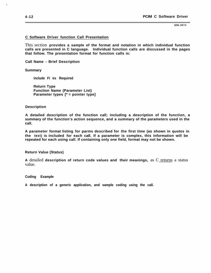
4-12 PCIM C Software Driver
GFK-0074
C Software Driver function Call Presentation
This section provides a sample of the format and notation in which individual functioncalls are presented in C language. Individual function calls are discussed in the pagesthat follow. The presentation format for function calls is:
Call Name - Brief Description
Summary
include Fi ies Required
Return TypeFunction Name (Parameter List)Parameter types [* = pointer type]
Description
A detailed description of the function call; including a description of the function, asummary of the function’s action sequence, and a summary of the parameters used in thecall.
A parameter format listing for parms described for the first time (as shown in quotes inthe text) is included for each call. If a parameter is complex, this information will berepeated for each using call. If containing only one field, format may not be shown.
Return Value (Status)
A detailed description of return code values and their meanings, as C returns a statusvalue.
Coding Example
A description of a generic application, and sample coding using the call.
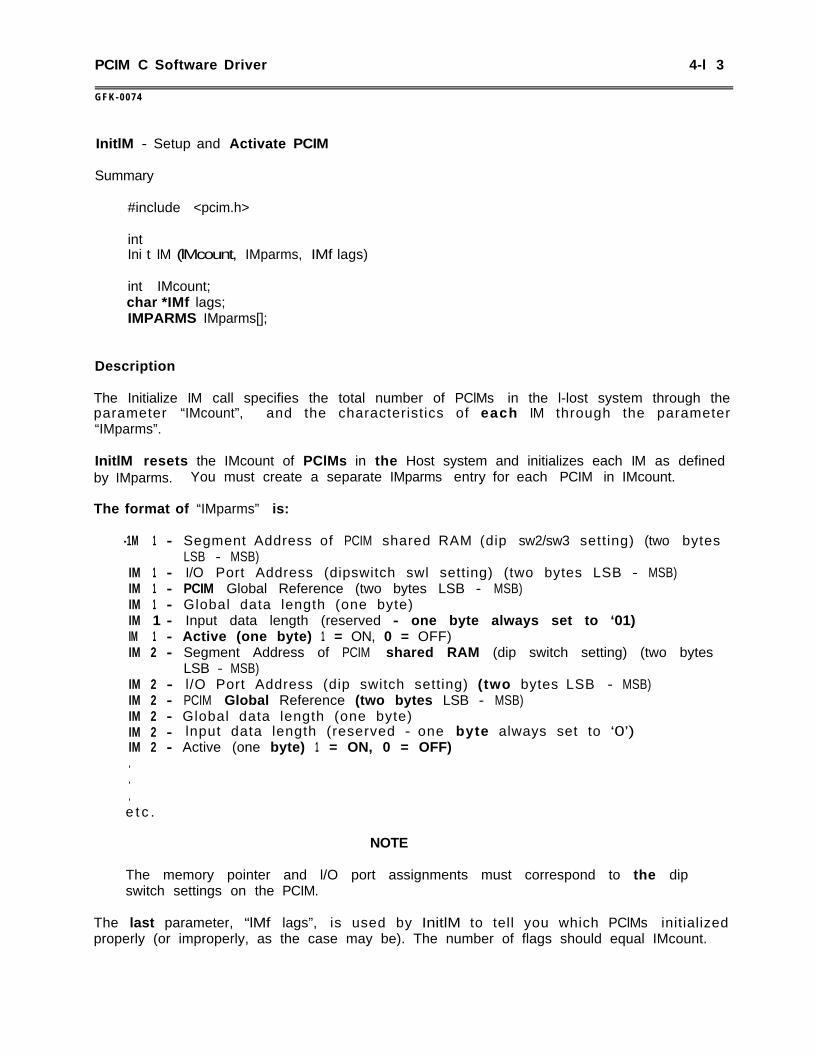
PCIM C Software Driver 4-l 3
G F K - 0 0 7 4
InitlM - Setup and Activate PCIM
Summary
#include <pcim.h>
intIni t IM (lMcount, IMparms, IMf lags)
int IMcount;char *IMf lags;IMPARMS IMparms[];
Description
The Initialize IM call specifies the total number of PClMs in the l-lost system through theparameter “IMcount”, and the characteristics of each IM through the parameter“IMparms”.
InitlM resets the IMcount of PClMs in the Host system and initializes each IM as definedby IMparms. You must create a separate IMparms entry for each PCIM in IMcount.
The format of “IMparms” is:
-1M 1 -
IM 1 -IM 1 -IM 1 -IM 1 -IM 1 -IM 2 -
IM 2 -IM 2 -IM 2 -IM 2 -IM 2 -...e t c .
Segment Address of PCIM shared RAM (dip sw2/sw3 setting) (two bytesLSB - MSB)I/O Port Address (dipswitch swl setting) (two bytes LSB - MSB)PCIM Global Reference (two bytes LSB - MSB)Global data length (one byte)Input data length (reserved - one byte always set to ‘01)Active (one byte) 1 = ON, 0 = OFF)Segment Address of PCIM shared RAM (dip switch setting) (two bytesLSB - MSB)l/O Port Address (dip switch setting) (two bytes LSB - MSB)PCIM Global Reference (two bytes LSB - MSB)Global data length (one byte)lnput data length (reserved - one byte always set to ‘0’)Active (one byte) 1 = ON, 0 = OFF)
NOTE
The memory pointer and l/O port assignments must correspond to the dipswitch settings on the PCIM.
The last parameter, “lMf lags”, is used by InitlM to tell you which PClMs initializedproperly (or improperly, as the case may be). The number of flags should equal IMcount.
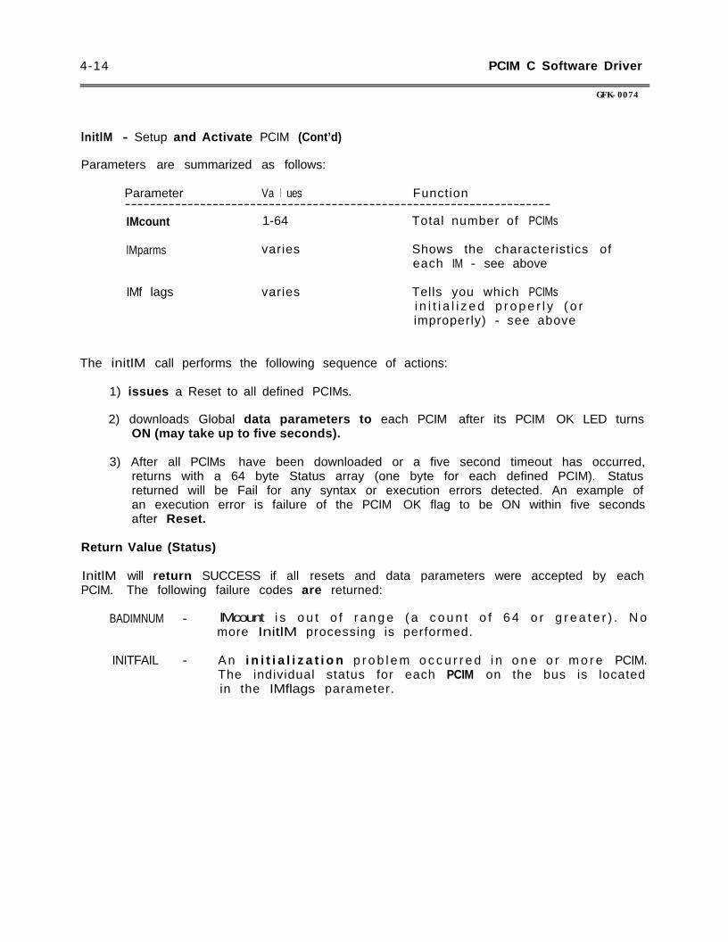
4-14 PCIM C Software Driver
GFK-0074
lnitlM - Setup and Activate PCIM (Cont’d)
Parameters are summarized as follows:
Parameter Va l ues Function--------------------------------------------------------------------IMcount 1-64 Total number of PClMs
lMparms varies Shows the characteristics ofeach IM - see above
IMf lags varies Tells you which PClMsi n i t i a l i z e d p r o p e r l y ( o rimproperly) - see above
The initlM call performs the following sequence of actions:
1) issues a Reset to all defined PCIMs.
2) downloads Global data parameters to each PCIM after its PCIM OK LED turnsON (may take up to five seconds).
3) After all PClMs have been downloaded or a five second timeout has occurred,returns with a 64 byte Status array (one byte for each defined PCIM). Statusreturned will be Fail for any syntax or execution errors detected. An example ofan execution error is failure of the PCIM OK flag to be ON within five secondsafter Reset.
Return Value (Status)
InitlM will return SUCCESS if all resets and data parameters were accepted by eachPCIM. The following failure codes are returned:
BADIMNUM - lMcount i s o u t o f r a n g e ( a c o u n t o f 6 4 o r g r e a t e r ) . N omore InitlM processing is performed.
INITFAIL - An i n i t i a l i z a t i o n p r o b l e m o c c u r r e d i n o n e o r m o r e PCIM.The individual status for each PCIM on the bus is locatedin the IMflags parameter.

PCIM C Software Driver 4-1 5
GFK-0074
InitlM - Setup and Activate PCIM (Cont’d)
One of the following status codes will be stored in the appropriate location in the IMflagsparameter if the return code is INITFAIL. Each status value in the IMflags array isunique to the associated PCIM and does not reflect the status of any other PCIM.
SUCCESS - This PCIM has been powered up and configured as specified.
IMFAIL - This PCIM never powered up.
BADCFG - This PCIM rejected the configuration because a parameterwas out of range.
BADSEG - The segment value in IMparms is set to the il legal value 0(zero).
BADPORT - The I/O port address is set to some il legal value less than256.
NOTE
If any of the PCIMs fail to initialize as you have specified in IMparms, InitlMturns OFF the failed PCIM.
Coding Example
In this example are two PCIMs.
#include <pcim.h>
#define COUNT 2
int status; char lMf Iags[COUNT];IMPARMS IMparms[COUNT];
lMparms[0].im.Segment = 0xD000; */SRI begins at D000(h) /*IMparms[0].im.lOPort = 0x3E4; */Port Base Address at 3E4(h)/*IMparms[0].lMRef = 0x7000; */PCIM Global Reference - 7000(h)/*IMparm0].OutputLength = 0; */No Global Data/*IMpatms[O].lnputLength = 0 ; */Always set to ‘0’/*lMparms[0].Active = ON; */Turn PCIM #l ON by default/*
fMparms[l].im.Segment = OxCCOO;IMparms[l]. im. IOPort = Ox3EO;lMparms[l].lMRef = 0x3000;IMparms[l].OutputLength = 0 ;IMparms[l].lnputLength = 0;IMparms[l].Active = ON;
*/SRI begins at CCOO(h)/**/Port Base Address at 3EO(hV**/PCIM Global Reference - 3000(h)/**/No Global Data/**‘/Always set to ‘O’/**/Turn PCIM #2 ON by default/*
s t a t u s = InitlM (COUNT, IMparms, IMflags);

4-16 PCIM C Software Driver
GFK-0074
ChglMSetup - Change PClM Configuration
Summary
#include <pcim.h>
intChglMSetup (IMnum, IMparms)
int IMnum;IMPARMS *lMparms;
Description
Following initialization, any changes you make to the configuration of a specific PCIMmust use the Change IM Setup call. This call allows you to make configuration changes toa specific PClM Setup Table by writing the IMparms parameter from Host memory to it.
The “IMnum” parameter is an offset of the IMparms parameter which, after initialization,indicates the specific PCIM in the host system for which configuration changes areintended. The relative IMnum cannot itself be changed.
NOTE
Configuration changes to any PClM while online causes that IM to stoptransmitting on the serial bus for 1.5 seconds.
Again, the format of “IMparms" is:
IM 1 - Segment Address of PCIM shared RAM (dip switch setting) (two bytesLSB - MSB)
1M 1 - l/O Port Address (dipswitch setting) (two bytes LSB - MSB)IM 1 - PCIM Global Reference (two bytes LSB - MSB)IM 1 - Global data length (one byte)IM 1 - Input data length (reserved - one byte always set to 0 )IM 1 - Active (one byte) 1 = ON, 0 = OFF)IM 2 - Segment Address of PCIM shared RAM (dip switch setting) (two bytes
LSB - MSB)IM 2 - l/O Port Address (dip switch setting) (two bytes LSB - MSB)IM 2 - PClM Global Reference (two bytes LSB - MSB)IM 2 - Global data length (one byte)IM 2 - Input data length (reserved - one byte always set to ‘0’)IM 2 - Active (one byte) 1 = ON, 0 = OFF)e t c .
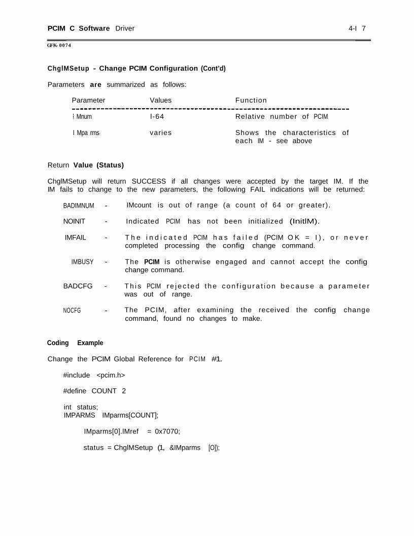
PCIM C Software Driver 4-I 7
GFK-0074
ChglMSetup - Change PCIM Configuration (Cont’d)
Parameters are summarized as follows:
Parameter Values Function--------------------______________l__l__----------------------------I Mnum l-64 Relative number of PCIM
I Mpa rms varies Shows the characteristics ofeach IM - see above
Return Value (Status)
ChglMSetup will return SUCCESS if all changes were accepted by the target IM. If theIM fails to change to the new parameters, the following FAIL indications will be returned:
BADIMNUM -
NOINIT -
IMFAIL -
IMBUSY -
BADCFG -
NOCFG -
Coding Example
IMcount is out of range (a count of 64 or greater).
Indicated PCIM has not been initialized (InitlM).
T h e i n d i c a t e d PCIM h a s f a i l e d (PCIM O K = I ) , o r n e v e rcompleted processing the config change command.
The PCIM is otherwise engaged and cannot accept the configchange command.
T h i s PCIM r e j e c t e d t h e c o n f i g u r a t i o n b e c a u s e a p a r a m e t e rwas out of range.
The PCIM, after examining the received the config changecommand, found no changes to make.
Change the PCIM Global Reference for PCIM #1.
#include <pcim.h>
#define COUNT 2
int status;IMPARMS IMparms[COUNT];
IMparms[0].lMref = 0x7070;
status = ChglMSetup (1, &IMparms [O]);
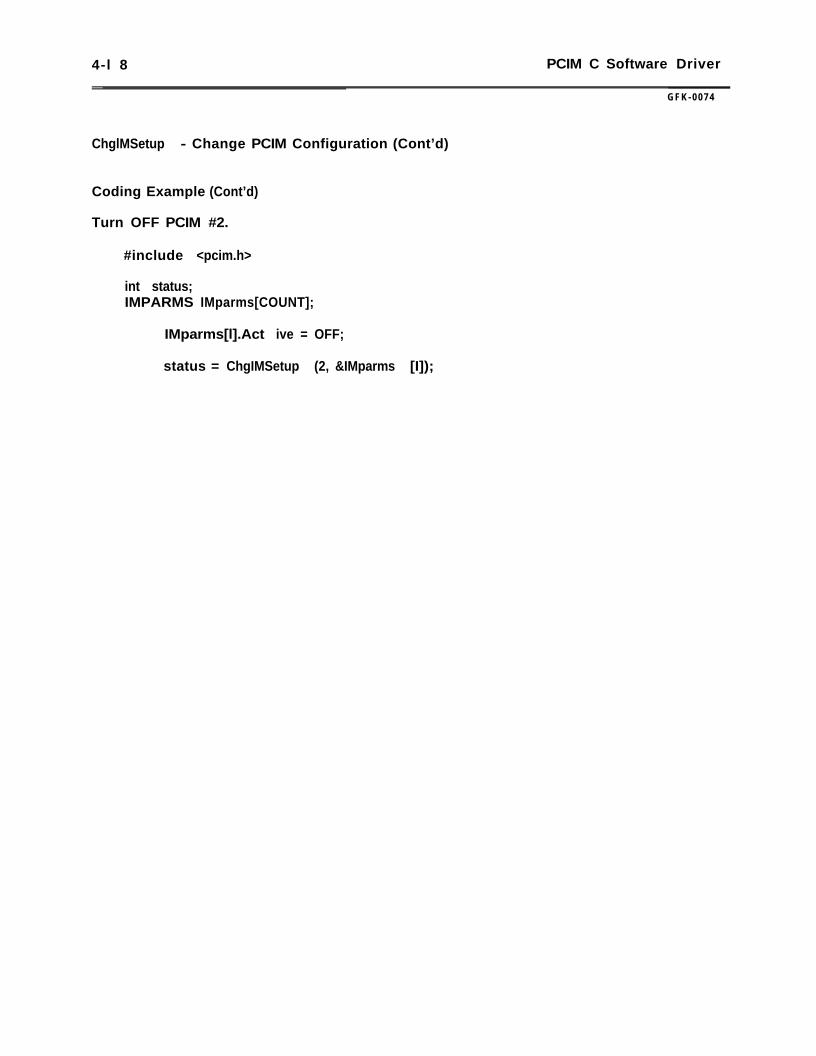
4-l 8 PCIM C Software Driver
G F K - 0 0 7 4
ChglMSetup - Change PCIM Configuration (Cont’d)
Coding Example (Cont’d)
Turn OFF PCIM #2.
#include <pcim.h>
int status;IMPARMS IMparms[COUNT];
IMparms[l].Act ive = OFF;
status = ChgIMSetup (2, &IMparms [I]);
PCIM C Software Driver 4-l 9
G F K - 0 0 7 4
GetlMState - Get Configuration and Status Information
Summary
#include <pcim.h>
intGetlMState (IMnurn, IMstate)
int IMnum;IMSTATE *lMstate;
Description
The Get IM State call allows you to access configuration and status information about aspecific PCIM by reading its Setup Table and Status Table into the “IMstate" parameter inHost memory.
The format of IMstate is:
DipSwi tch - Daugherboard Dip Switch ValueIMRef - Reference AddressOutputLength - Output Control Data LengthInputLength - Input Control Data Length
R e v i s i o n - PCIM Firmware Revision NumberGENI OK - PCIM OKFau It
= 0 - every 200 ms, set to ‘1’- Overall fault byte - any PCIM fault
Active - Hand Held Monitor PresentSBerr - Serial Bus error countScanTime - Bus Scan Time in ms
Before returning, GetlMState will also clear the PCIM OK flag of the selected PCIM.Since the PCIM periodically sets its PCIM OK flag, this call allows the implementation ofa PCIM OK heartbeat procedure.
Parameters are summarized as follows:
Parameter Values Function____3-_----__-11-___c_c______________I__----------------------------I Mnum l - 6 4 Relative number of PCIM
IMstate varies PCIM Configuration andStatus -see above
4-20 PCIM C Software Driver
GFK-0074
CetlMState - Get Configuration and Status Information (Cont’d)
Return Value (Status)
GetlMState will almost always return SUCCESS. If the target IM is currently offline, hasnot been initialized, or is out of range, the following FAIL indications will be returned:
BADIMNUM - IMcount is out of range (a count of 64 or greater).
NOlNlT - Indicated PCIM has not been initialized (InitIM).
lMFAlL - The indicated PClM has failed (PCIM OK = 1).
Coding Example
Examine the state of PCIM #1.
#include <pcim.h>
int status;IMSTATE IMstate;
status = GetlMState (1, &IMstate);
PCIM C Software Driver 4-21
CFK-0074
GetBusConfig - Get Serial Bus Configuration
Summary
#include <pcim.h>
intGetBusConf ig (IMnum, Config)
int IMnum;DEVICE Conf ig[];
Description
The Get Bus Configuration call allows you to read device configuration information aboutall devices on a serial bus. GetBusConf ig reads all 32 Device Configuration Tables f tomthe PClM selected by IMnum into the Host memory “Config” parameter. This informationis not packed and wilt fill the entire Config parm - 256 bytes in length.
The format of Config is:
unsigned char Model - Model Number of deviceunsigned char OutputDisable - Output disable flagunsigned char Present - Device Present flagunsigned int Reference - S t a t u s T a b l e o r
- Reference Addressunsigned char InputLength - C o n t r o l I n p u t D a t a l e n g t hunsigned char OutputLength - Control Output Data Lengthunsigned char Config - D e v i c e C o n f i g u r a t i o n
Not UsedBlock Conf ig -----------------------------+---+
Parameters are summarized as follows:
Parameter Values Function--------------------------------------------------------------------I Mnum l-64 Relative number of PCIM
Conf ig 256 bytes Device configurationi n f o r m a t i o n a b o u t a l ldevices on a serial bus- see above
4-22 PCIM C Software Driver
GFK-0074
GetBusConf ig - Get Serial Bus Configuration (Cont’d)
Return Value (Status)
GetBusConfig will almost always return SUCCESS. If the target IM is currently off line,has not been initialized, or is out of range, the following FAIL indications will be returned:
BADIMNUM - IMcount is out o range (a count of 64 or greater).
NOINIT - Indicated PCIM has not been initialized (InitlM).
IMFAIL - The indicated PCIM has failed (PCIM OK = 1).
OFFL INE - None of the devices specified are currently active on thebus. However, the appropriate buffer is sti l l returned andw i I I c o n t a i n c o n f i g u r a t i o n d a t a f o r d e v i c e s o n c ein.
I oggedZeros wi I I be returned if no device has logged in t o a
p a r t i c u l a r s l o t .
Coding Example
Examine the configuration of the devices on PCIM #1.
#include <pcim.h>int status;DEVICE Conf ig[MAXDEVlCE];
status = GetBusConf ig (1, Conf ig);
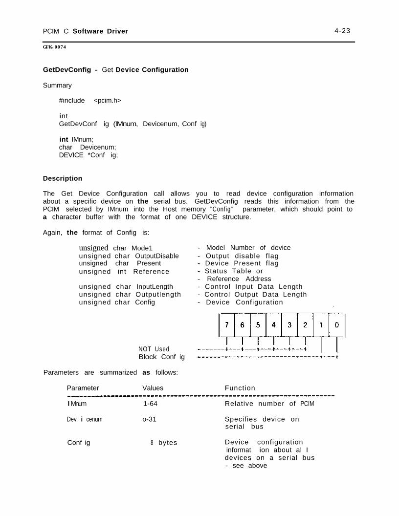
PCIM C Software Driver 4-23
GFK-0074
GetDevConfig - Get Device Configuration
Summary
#include <pcim.h>
intGetDevConf ig (IMnum, Devicenum, Conf ig)
int IMnum;char Devicenum;DEVICE *Conf ig;
Description
The Get Device Configuration call allows you to read device configuration informationabout a specific device on the serial bus. GetDevConfig reads this information from thePCIM selected by IMnum into the Host memory "Config" parameter, which should point toa character buffer with the format of one DEVICE structure.
Again, the format of Config is:
unsigned char Mode1 - Model Number of deviceunsigned char OutputDisable - Output disable flagunsigned char Present - Device Present flagunsigned int Reference - Status Table or
- Reference Addressunsigned char InputLength - Control Input Data Lengthunsigned char Outputlength - Control Output Data Lengthunsigned char Config - Device Configuration
NOT Used -----~Block Conf ig -------------------------------t---t
Parameters are summarized as follows:
Parameter Values Function--------------------___________c__I_____----------------------------I Mnum 1-64 Relative number of PCIM
Dev i cenum o-31 Specifies device onserial bus
Conf ig 8 bytes Device configurationinformat ion about al Idevices on a serial bus- see above
4-24 PCIM C Software Driver
CFK-0074
GetDevConf ig - Get Device Configuration (Cont’d)
Return Value (Status)
GetDevConfig will almost always return SUCCESS. If the target IM is currently offline,has not been initialized, or is out of range, the following FAIL indications will be returned:
BADIMNUM - IMcount is out of range (a count of 64 or greater).
BADSBA - Speci f ied Devicenum is not in the range for GENIUS busdevices (0 -31 decimal).
NOINIT - Indicated PCIM has not been initialized (InitlM).
IMFAIL - The indicated PCIM has fai led (PCIM OK = 1), or nevercompleted processing the config change command.
OFFL INE - The device requested is currently not on the bus, however,the appropriate buffer is sti II returned and wi ll containconfiguration data for devices once logged in.
Coding Example
Examine the configuration of device #30 on PCIM #1.
#include <pcim.h>
int status;DEVICE Conf igbuf;
status = GetDevConf ig (1, 30, Conf igbuf);
PCIM C Software Driver 4-25
GFK-0074
DisableOut - Disable/Enable Device Outputs
Summary
#include <pcim.h>
intDisableOut (IMnum, Devicenum, Flag)
int IMnum, Devicenum;char Flag;
Description
The Disable (/Enable) Outputs call allows you to selectively disable (or enable) outputs toa specific device, or to all devices, on a serial bus.
If Flag is non-zero (‘1’), outputs to the device will be disabled; if Flag is zero (‘0’),outputs will be enabled to that device. If you code the Devicenum value equal to ‘ALL’,then the outputs to all devices will be set to the value of Flag. If Devicenum is a serialbus address value between 0 - 31 decimal, then the flag value will only affect thatdevice. PCIM.H contains macros defined for ON or OFF values for Flag.
Parameters are summarized as follows:
Parameter Values Function-------I--------c11-II-------------------------------------------------I Mnum l - 6 4 Relative number of PCIM
Dev i cenum O-31 Specifies device onserial bus on whichci rcui t resides
Flag 0 or 1 Enable/disable outputs
Return Value (Status)
DisableOut will return SUCCESS if the device specified by IMnum is present on the serialbus. Otherwise, DisableOut w i l l r e t u r n F A I L . If Devicenum indicates ALL, thenDisableOut will almost always return SUCCESS. The following FAIL indications will bereturned:
BADIMNUM - IMCount is out of range (a count of 64 or greater).
BADSBA - Specified Devicenum is not in the range for GENIUS busdevices (0 - 31 decimal).
NOlNlT - Indicated PCIM has not been initialized (InitlM).
IMFAIL - The indicated PCIM has failed (PCIM OK = 1).
4-26 PCIM C Software Driver
GFK-0074
DisableOut - Disable/Enable Device Outputs (Cont’d)
Coding Example
Enable outputs to device #8 on PCIM #1.
#include <pcim.h>
int status;
status = DisableOut (1, 8, ENABLE);
Disable outputs to all devices on PCIM #1.
#include <pcim.h>
int status;
status = DisableOut (2, All, DISABLE);
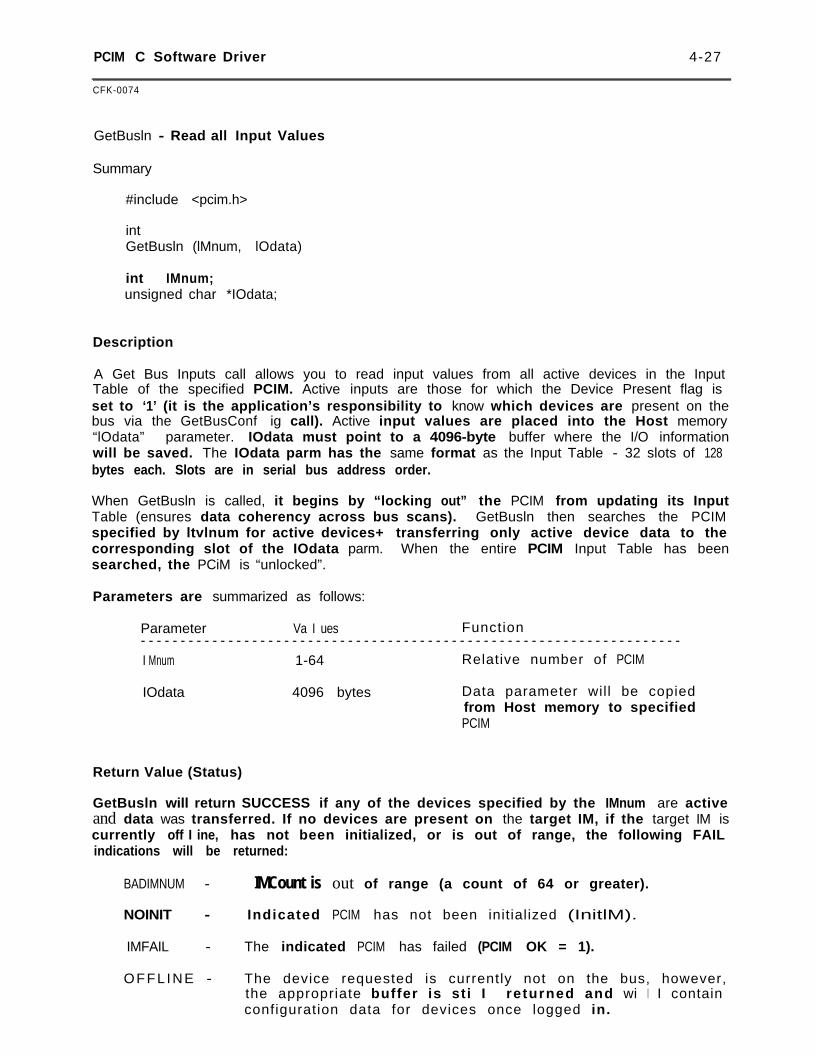
PCIM C Software Driver 4-27
CFK-0074
GetBusln - Read all Input Values
Summary
#include <pcim.h>
intGetBusln (lMnum, lOdata)
int IMnum;unsigned char *IOdata;
Description
A Get Bus Inputs call allows you to read input values from all active devices in the InputTable of the specified PCIM. Active inputs are those for which the Device Present flag isset to ‘1’ (it is the application’s responsibility to know which devices are present on thebus via the GetBusConf ig call). Active input values are placed into the Host memory“lOdata” parameter. IOdata must point to a 4096-byte buffer where the I/O informationwill be saved. The IOdata parm has the same format as the Input Table - 32 slots of 128bytes each. Slots are in serial bus address order.
When GetBusln is called, it begins by “locking out” the PCIM from updating its InputTable (ensures data coherency across bus scans). GetBusln then searches the PCIMspecified by ltvlnum for active devices+ transferring only active device data to thecorresponding slot of the IOdata parm. When the entire PCIM Input Table has beensearched, the PCiM is “unlocked”.
Parameters are summarized as follows:
Parameter Va I ues Function- - - - - - - - - - - - - - - - - - - - - - - - - - - - - - - - - - - - - - - - - - - - - - - - - - - - - - - - - - - - - - - - - - - -I Mnum 1-64 Relative number of PCIM
IOdata 4096 bytes Data parameter will be copiedfrom Host memory to specifiedPCIM
Return Value (Status)
GetBusln will return SUCCESS if any of the devices specified by the IMnum are activeand data was transferred. If no devices are present on the target IM, if the target IM iscurrently off I ine, has not been initialized, or is out of range, the following FAILindications will be returned:
BADIMNUM - IMCount is out of range (a count of 64 or greater).
NOINIT - Indicated PCIM has not been initialized (InitlM).
IMFAIL - The indicated PCIM has failed (PCIM OK = 1).
OFFLINE - The device requested is currently not on the bus, however,the appropriate buffer is sti I returned and wi I I containconfiguration data for devices once logged in.

4-28 PCIM C Software Driver
G F K - 0 0 7 4
GetBusln - Read all Input Values (Cont’d)
Coding Example
Read all inputs from all active devices on PCIM #1.
#include <pcim.h>
int status;unsigned char IOdata[4096];
status = GetBusln (1, IOdata);
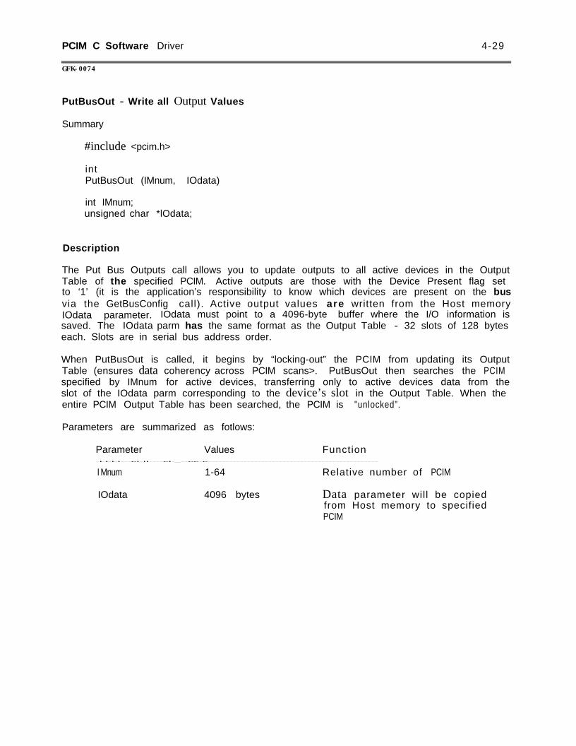
PCIM C Software Driver 4-29
GFK-0074
PutBusOut - Write all Output Values
Summary
#include <pcim.h>
intPutBusOut (IMnum, IOdata)
int IMnum;unsigned char *lOdata;
Description
The Put Bus Outputs call allows you to update outputs to all active devices in the OutputTable of the specified PCIM. Active outputs are those with the Device Present flag setto ‘1’ (it is the application’s responsibility to know which devices are present on the busvia the GetBusConfig call). Active output values are written from the Host memoryIOdata parameter. IOdata must point to a 4096-byte buffer where the I/O information issaved. The IOdata parm has the same format as the Output Table - 32 slots of 128 byteseach. Slots are in serial bus address order.
When PutBusOut is called, it begins by “locking-out” the PCIM from updating its OutputTable (ensures data coherency across PCIM scans>. PutBusOut then searches the PCIMspecified by IMnum for active devices, transferring only to active devices data from theslot of the IOdata parm corresponding to the device’s slot in the Output Table. When theentire PCIM Output Table has been searched, the PCIM is "unlocked”.
Parameters are summarized as fotlows:
Parameter Values Function-LLLI---cI-II----cI-_--cc-c------------------------------------------------
I Mnum 1-64 Relative number of PCIM
IOdata 4096 bytes Data parameter will be copiedfrom Host memory to specifiedPCIM
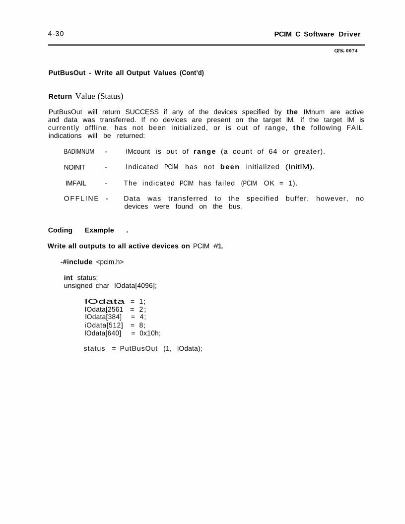
4-30 PCIM C Software Driver
GFK-0074
PutBusOut - Write all Output Values (Cont’d)
Return Value (Status)
PutBusOut will return SUCCESS if any of the devices specified by the IMnum are activeand data was transferred. If no devices are present on the target IM, if the target IM iscurrently offl ine, has not been init ialized, or is out of range, the following FAILindications will be returned:
BADIMNUM - IMcount is out of range (a count of 64 or greater).
NOINIT - Indicated PCIM has not been initialized (InitlM).
IMFAIL - The indicated PCIM has failed (PCIM OK = 1).
OFFL INE - Data was transferred to the specified buffer, however, nodevices were found on the bus.
Coding Example .
Write all outputs to all active devices on PCIM #1.
-#include <pcim.h>
int status;unsigned char lOdata[4096];
lOdata = 1;IOdata[2561 = 2 ;lOdata[384] = 4;iOdata[512] = 8;lOdata[640] = 0x10h;
status = PutBusOut (1, lOdata);
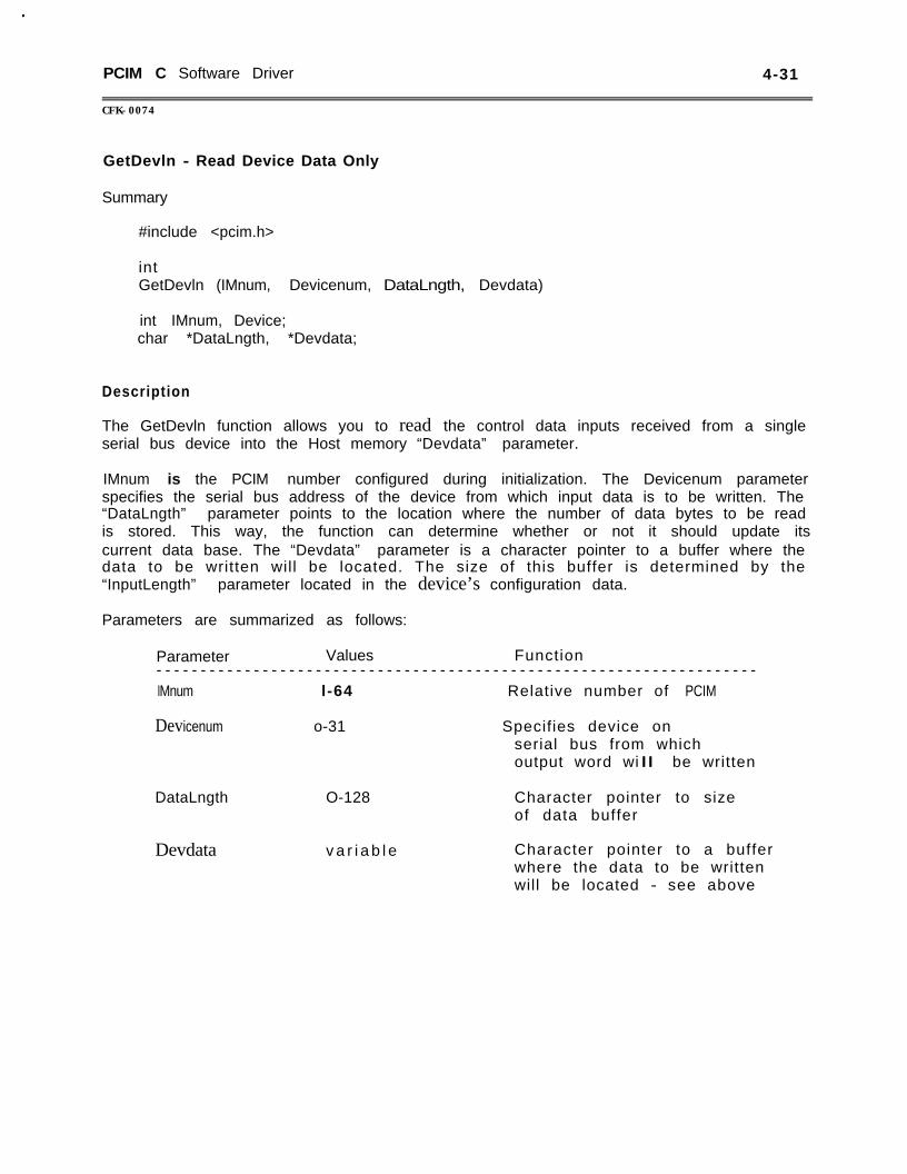
PCIM C Software Driver 4-31
CFK-0074
GetDevln - Read Device Data Only
Summary
#include <pcim.h>
intGetDevln (IMnum, Devicenum, DataLngth, Devdata)
int IMnum, Device;char *DataLngth, *Devdata;
Description
The GetDevln function allows you to read the control data inputs received from a singleserial bus device into the Host memory “Devdata” parameter.
IMnum is the PCIM number configured during initialization. The Devicenum parameterspecifies the serial bus address of the device from which input data is to be written. The“DataLngth” parameter points to the location where the number of data bytes to be readis stored. This way, the function can determine whether or not it should update itscurrent data base. The “Devdata” parameter is a character pointer to a buffer where thedata to be written will be located. The size of this buffer is determined by the“InputLength” parameter located in the device’s configuration data.
Parameters are summarized as follows:
Parameter Values Function- - - - - - - - - - - - - - - - - - - - - - - - - - - - - - - - - - - - - - - - - - - - - - - - - - - - - - - - - - - - - - - - - - - -IMnum l-64 Relative number of PCIM
Devicenum o-31 Specifies device onserial bus from whichoutput word wi II be written
DataLngth O-128 Character pointer to sizeof data buffer
Devdata v a r i a b l e Character pointer to a bufferwhere the data to be writtenwill be located - see above
4-32 PCIM C Software Driver
GFK-0074
GetDevln - Read Device Data Only
Return Value (Status)
GetDevln will return SUCCESS if the device specified by IMnum is present on the serialbus, and after the data is transferred to the DevData buffer. If the target device is notpresent, or is out of range, the following FAlL indications will be returned:
BAD IMNUM - IMcount is out of range (a count of 64 or greater).
BADSBA - Specified Devicenum is not in the range for GENIUS busdevices (0 -31 decimal), or is that of the PCIM - which hasits own function.
NOINlT - Indicated PClM has not been initialized (InitlM).
IMFAIL - The indicated PCIM has failed (PCIM OK = 1).
OFFLINE - The device requested is currently not on the bus, and datais NOT transferred.
Coding Example
Get the inputs from device #8 on PC I M #1 .
#include <pcim.h>
int status;unsigned char Devdata[l28];
Length;
status = GetDevln (1, 8, &Length, Devdata);
PCIM C Software Driver 4-33
GFK-0074
PutDevOut - Write Device Data Only
Summary
#include <pcim.h>
intPutDevOut (IMnum, Devicenum, Datalngth, Devdata)
int M-turn, Device;char DataLngth, *Devdata;
Description
The PutDevOut call allows you to write all of the control data outputs to a single serialbus device from the Host memory Devdata parameter.
IMnum is the PCIM number configured during initialization. The Devicenum parameterspecifies the serial bus address of the device to which output data is to be written. TheDataLngth parameter points to the location where the number of data bytes to write isstored. If the value differs from the PClM’s current data base, an Overflow or Underflowerror will be returned. The Devdata parameter is a character pointer to a buffer wherethe data to be written is located. The size of this buffer is determined by the"OutputLength” parameter located in the device’s configuration data.
Parameters are summarized as follows:
Parameter Values Function--------------------_______I____________----------------------------I Mnum 1-64 Relative number of PCIM
Dev i cenum o-31 Specifies device to whichoutput word will be written
Datalngth O - 1 2 8 Character pointer to sizeof data buffer
Devdata v a r i a b l e Character pointer to a bufferwhere the data to be writtenwill be located - see above
c
4-34 PCIM C Software Driver>
CFK-0074
PutDevOut - Write Device Data Only
Return Value (Status)
PutDevOut will return SUCCESS if the device indicated is present on the given IMnumand after the data is transferred to that device. If the target device is not present, or isout of range, the following FAIL indications will be returned:
BADIMNUM - IMcount is out of range (a count of 64 or greater).
BADSBA - Specified Devicenum is not in the range for GENIUS busdevices (0 -31 decimal), or is that of the PCIM - which hasits own function.
NOINIT - Indicated PCIM has not been initialized (InitlM).
IMFAIL - The indicated PCIM has failed (PCIM OK = 1).
OFFL INE - The device requested is currently not on the bus, and datais NOT transferred.
Coding Example
Write 2 bytes of output data to device #8 on PCIM #1.
#include <pcim.h>
int.status;unsigned char Devdata[l28];
Devdata [O] = 1;Devdata [l] = 0x10;
status = PutDevOut (1, 8, 2, Devdata);

PCIM C Software Driver 4-35
GFK-0074
GetlMIn - Read Directed Input Table
Summary
#include <pcim.h>
intGetlMln (IMnum, IMdata)
int IMnum;unsigned char *IMdata;
Description
The Get IM Inputs call is reserved and should not be used.
4-36 PCIM C Software Driver
GFK-0074
PutlMOut - Write the Global Output Table
Summary
#include <pcim.h>
intPutlMOut ( I M n u n , IMdata)
int IMnum;unsigned char *IMdata;
Description
The Put IM Outputs call allows you to write Global Data from the Host memory IMdataparameter to the Output Table of a specified PCIM. This data is subsequently broadcastto all CPUs on the bus every bus scan.
IMnum is the PCIM number configured during initialization. The IMdata parameter is acharacter pointer to a buffer where the data to be written is located. The size of thisbuffer is determined by the “OutputLength” Global Data Length) parameter located inthe device’s configuration data.
When PutlMOut is called, it begins by “Iocking-out” the PCIM from reading from itsOutput Table (ensures data coherency across bus scans). PutlMOut then transfers all thedata from this parm to the PCIM’s Global Output buffer. Once the transfer is complete,the PClM is “unlocked”.
Parameters are summarized as follows:
Parameter Values Function--------------------________I___________----------------------------I Mnum 1-64 Relative number of PCIM
IMdata variable Character pointer to a bufferwhere the data is located.Length of buffer is equal tooutput length as specified inInitlM.
Return Value (Status)
PutlMOut will return SUCCESS if the GlobalLength is non-zero and the transfer iscomplete, The following FAIL indications will be returned:
BADIMNUM - IMcount is out of range (a count of 64 or greater).
NOINlT - Indicated PCIM has not been initialized (InittM).
IMFAIL - The indicated PCIM has failed (PCIM OK = 1).
UNDERFLOW - The GlobalLength parameter in PARMS is set to zero (0).
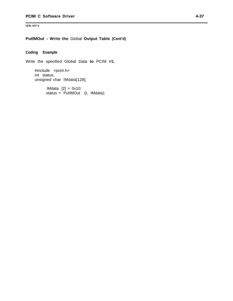
PCIM C Software Driver 4-37
GFK-0074
PutlMOut - Write the Global Output Table (Cont’d)
Coding Example
Write the specified Global Data to PCIM #1.
#include <pcim.h>int status;unsigned char IMdata[128];
IMdata [2] = 0x10;status = PutIMOut (I, IMdata);
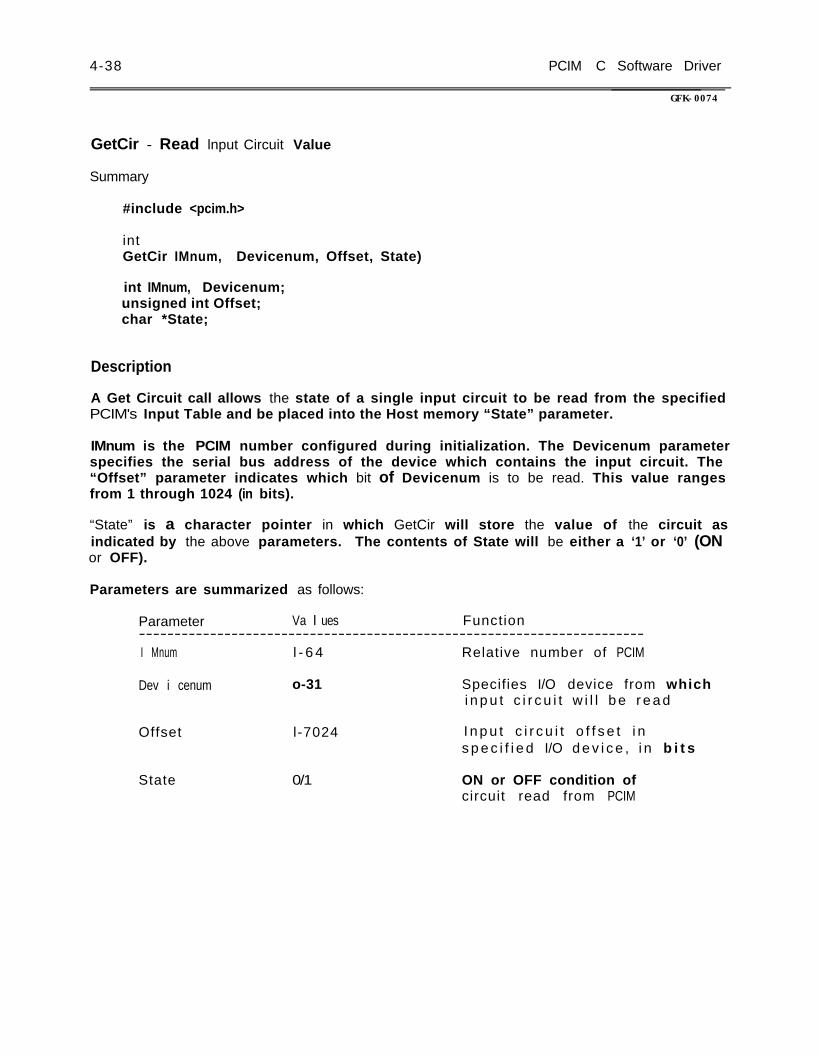
4-38 PCIM C Software Driver
GFK-0074
GetCir - Read lnput Circuit Value
Summary
#include <pcim.h>
intGetCir IMnum, Devicenum, Offset, State)
int IMnum, Devicenum;unsigned int Offset;char *State;
Description
A Get Circuit call allows the state of a single input circuit to be read from the specifiedPCIM's Input Table and be placed into the Host memory “State” parameter.
IMnum is the PCIM number configured during initialization. The Devicenum parameterspecifies the serial bus address of the device which contains the input circuit. The“Offset” parameter indicates which bit of Devicenum is to be read. This value rangesfrom 1 through 1024 (in bits).
“State” is a character pointer in which GetCir will store the value of the circuit asindicated by the above parameters. The contents of State will be either a ‘1’ or ‘0’ (ONor OFF).
Parameters are summarized as follows:
Parameter Va l ues Function-----------------------------------------------------------------------I Mnum l - 6 4 Relative number of PCIM
Dev i cenum o-31 Specifies I/O device from whichi n p u t c i r c u i t w i l l b e r e a d
Offset l-7024 I n p u t c i r c u i t o f f s e t i ns p e c i f i e d I/O d e v i c e , i n b i t s
State 0/1 ON or OFF condition ofcircuit read from PCIM

PCIM C Software Driver 4-39-.
GFK-0074
GetCir - Read Input Circuit Value (Cont’d)
Return Vafue (Status)
GetCir will return SUCCESS if the target device is present on the given IMnum. If thetarget device is not present, or is out of range, GetCir will return FAIL. If SUCCESS isreturned, then the character pointed to by State will contain the value of the circuitrequested. The following FAIL indications will be returned:
BADIMNUM - IMCount is out of range (a count of 64 or greater).
BADSBA - Specified Devicenum is not in the range for GENIUS busdevices (0 -31 decimal), or is that of the PCIM - which hasits own function.
NOINIT - Indicated PCIM has not been initialized (InitlM).
IMFAIL - The indicated PCIM has failed (PCIM OK = 1).
OFFL INE - The device requested is currently not on the bus, and datais NOT transferred.
OVERFLOW - T h e O f f s e t specified i s greater than the devicesInputLength i n c i r c u i t s .
UNDERFLOW - The Offset is specified as zero (0).
Coding Example
Get the State value of circuit 2 of device #8 on PClM #1.
#include <pcim.h>
int status;char State;
status = GetCir (1, 8, 2, &State);
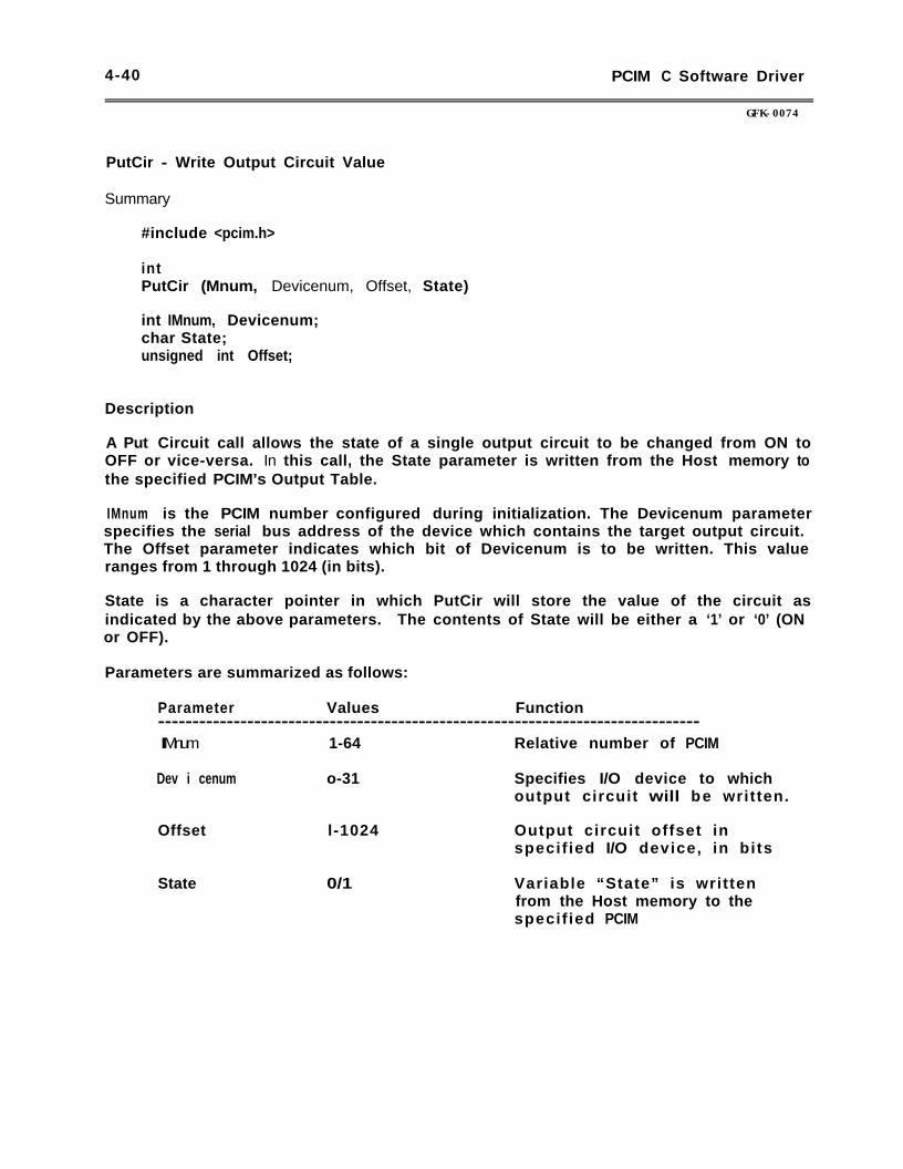
4-40 PCIM C Software Driver
GFK-0074
PutCir - Write Output Circuit Value
Summary
#include <pcim.h>
intPutCir (Mnum, Devicenum, Offset, State)
int IMnum, Devicenum;char State;unsigned int Offset;
Description
A Put Circuit call allows the state of a single output circuit to be changed from ON toOFF or vice-versa. In this call, the State parameter is written from the Host memory tothe specified PCIM’s Output Table.
IMnum is the PCIM number configured during initialization. The Devicenum parameterspecifies the serial bus address of the device which contains the target output circuit.The Offset parameter indicates which bit of Devicenum is to be written. This valueranges from 1 through 1024 (in bits).
State is a character pointer in which PutCir will store the value of the circuit asindicated by the above parameters. The contents of State will be either a ‘1’ or ‘0’ (ONor OFF).
Parameters are summarized as follows:
Parameter Values Function-------------------------------------------------------------------------------IIMnum 1-64 Relative number of PCIM
Dev i cenum o-31 Specifies I/O device to whichoutput circuit will be written.
Offset l-1024 Output circuit offset inspecif ied I/O device, in bits
State 0/1 Variable “State” is writtenfrom the Host memory to thespecif ied PCIM
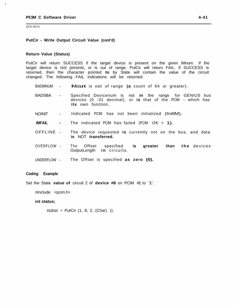
PCIM C Software Driver 4-41
GFK-0074
PutCir - Write Output Circuit Value (cont’d)
Return Value (Status)
PutCir will return SUCCESS if the target device is present on the given IMnum. If thetarget device is not present, or is out of range, PutCir will return FAIL. If SUCCESS isreturned, then the character pointed to by State will contain the value of the circuitchanged. The following FAIL indications will be returned:
BADIMNUM - IMcount is out of range (a count of 64 or greater).
BADSBA - Specified Devicenum is not in the range for GENIUS busdevices (0 -31 decimal), or is that of the PCIM - which hasits own function.
NOINlT - Indicated PCIM has not been initialized (InitlM).
IMFAIL - The indicated PCIM has failed (PCIM OK = 1).
OFFL INE - The device requested is currently not on the bus, and datais NOT transferred.
OVERFLOW - T h e Offset specified is greater than t h e d e v i c e sOutputLength i n c i r c u i t s .
UNDERFLOW - The Offset is specified as zero (0).
Coding Example
Set the State value of circuit 2 of device #8 on PCIM #1 to ‘1’.
#include <pcim.h>
int status;
status = PutCir (1, 8, 2, (Char) 1);
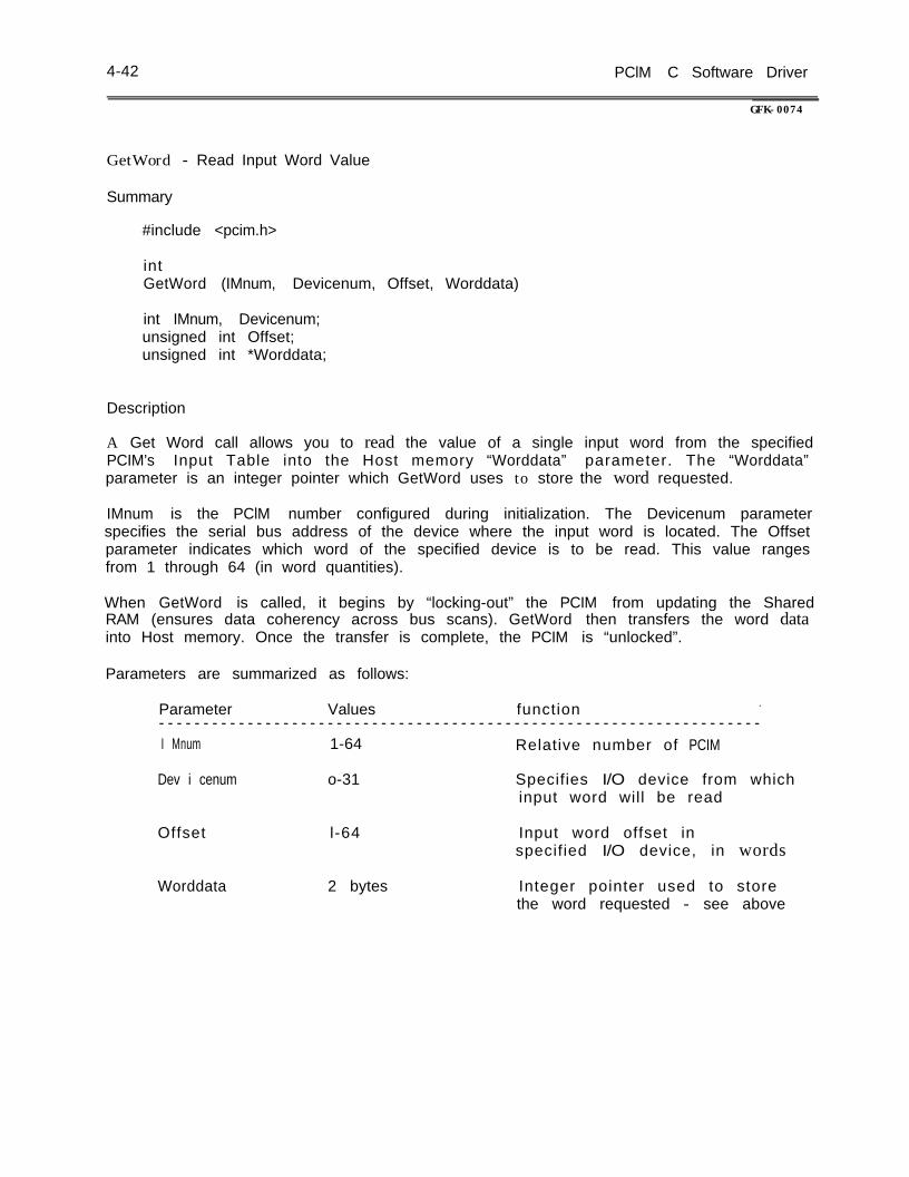
4-42 PClM C Software Driver
GFK-0074
GetWord - Read Input Word Value
Summary
#include <pcim.h>
intGetWord (IMnum, Devicenum, Offset, Worddata)
int IMnum, Devicenum;unsigned int Offset;unsigned int *Worddata;
Description
A Get Word call allows you to read the value of a single input word from the specifiedPCIM’s Input Table into the Host memory “Worddata” parameter. The “Worddata”parameter is an integer pointer which GetWord uses to store the word requested.
IMnum is the PClM number configured during initialization. The Devicenum parameterspecifies the serial bus address of the device where the input word is located. The Offsetparameter indicates which word of the specified device is to be read. This value rangesfrom 1 through 64 (in word quantities).
When GetWord is called, it begins by “locking-out” the PCIM from updating the SharedRAM (ensures data coherency across bus scans). GetWord then transfers the word datainto Host memory. Once the transfer is complete, the PCIM is “unlocked”.
Parameters are summarized as follows:
Parameter Values function .- - - - - - - - - - - - - - - - - - - - - - - - - - - - - - - - - - - - - - - - - - - - - - - - - - - - - - - - - - - - - - - - - - - -I Mnum 1-64 Relative number of PCIM
Dev i cenum o-31 Specifies I/O device from whichinput word will be read
Offset l-64 Input word offset inspecified I/O device, in words
Worddata 2 bytes Integer pointer used to storethe word requested - see above
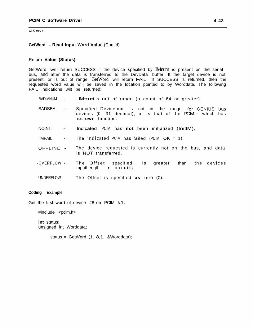
PCIM C Software Driver 4-43
GFK-0074
GetWord - Read Input Word Value (Cont’d)
Return Value (Status)
GetWord will return SUCCESS if the device specified by IMnum is present on the serialbus, and after the data is transferred to the DevData buffer. If the target device is notpresent, or is out of range, GetWord will return FAIL If SUCCESS is returned, then therequested word value will be saved in the location pointed to by Worddata. The followingFAIL indications wilt be returned:
BADIMNUM - IMcount is out of range (a count of 64 or greater).
BADSBA - Specified Devicenum is not in the range for GENIUS busdevices (0 -31 decimal), or is that of the PCIM - which hasits own function.
NOINIT - Indicated PClM has not been initialized (InitlM).
IMFAIL - The indicated PClM has failed (PCIM OK = 1).
OFFL INE - The device requested is currently not on the bus, and datais NOT transferred.
-OVERFLOW - T h e O f f s e t specified i s greater than t h e d e v i c e sInputLength i n c i r c u i t s .
UNDERFLOW - The Offset is specified as zero (0).
Coding Example
Get the first word of device #8 on PClM #1.
#include <pcim.h>
int status;unsigned int Worddata;
status = GetWord (1, 8,1, &Worddata);
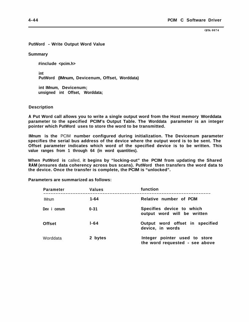
4-44 PCIM C Software Driver
GFK-0074
PutWord - Write Output Word Value
Summary
#include <pcim.h>
intPutWord (IMnum, Devicenum, Offset, Worddata)
int IMnum, Devicenum;unsigned int Offset, Worddata;
Description
A Put Word call allows you to write a single output word from the Host memory Worddataparameter to the specified PCIM’s Output Table. The Worddata parameter is an integerpointer which PutWord uses to store the word to be transmitted.
IMnum is the PCIM number configured during initialization. The Devicenum parameterspecifies the serial bus address of the device where the output word is to be sent. TheOffset parameter indicates which word of the specified device is to be written. Thisvalue ranges from 1 through 64 (in word quantities).
When PutWord is called, it begins by “locking-out” the PCIM from updating the SharedRAM (ensures data coherency across bus scans). PutWord then transfers the word data tothe device. Once the transfer is complete, the PCIM is “unlocked”.
Parameters are summarized as follows:
Parameter Values function--------------------------------------------------------------------
IMnum 1-64 Relative number of PCIM
Dev i cenum 0-31 Specifies device to whichoutput word will be written
Offset l-64 Output word offset in specifieddevice, in words
Worddata 2 bytes Integer pointer used to storethe word requested - see above
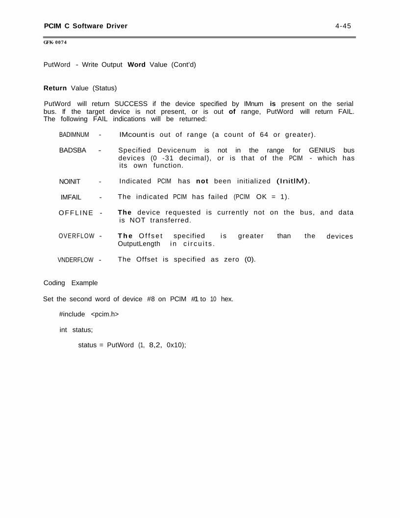
PCIM C Software Driver 4-45
GFK-0074
PutWord - Write Output Word Value (Cont’d)
Return Value (Status)
PutWord will return SUCCESS if the device specified by IMnum is present on the serialbus. If the target device is not present, or is out of range, PutWord will return FAIL.The following FAIL indications will be returned:
BADIMNUM - IMcount is out of range (a count of 64 or greater).
BADSBA - Specified Devicenum is not in the range for GENIUS busdevices (0 -31 decimal), or is that of the PCIM - which hasits own function.
NOINIT - Indicated PCIM has not been initialized (InitlM).
IMFAIL - The indicated PCIM has failed (PClM OK = 1).
OFFL INE - The device requested is currently not on the bus, and datais NOT transferred.
OVERFLOW - T h e O f f s e t specified i s greater than the devicesOutputLength i n c i r c u i t s .
VNDERFLOW - The Offset is specified as zero (0).
Coding Example
Set the second word of device #8 on PCIM #1 to 10 hex.
#include <pcim.h>
int status;
status = PutWord (1, 8,2, 0x10);

4-46 PCIM C Software Driver
GFK-0074
SendMsg - Send a Message
Summary
#include <pcim.h>
intSendMsg IMnum, Msg)
int IMnum;SEND-MESSAGE *Msg;
Description
The Send Message call allows you to write a memory or non-memory message from theHost to the selected PCIM for transmission onto the serial bus (using the TransmitDatagram command). SendMsg will return control to the calling program without delay,before the message has been processed or transmitted by the PCIM.
IMnum defines the PCIM, as configured during initialization, from which to transmit themessage. The Msg parameter is a pointer to the buffer where the transmit message isstored.
The format of SEND-MESSAGE is:
D e s t i n a t i o n (0-31/255 brdcst) - Destination address of Devicefunction code (0-111) - Function CodeSubFunction code (O-255) - Sub Function CodeP r i o r i t y - 0 - Normal, 1 - HighLength - Data field Length/length of messageData (O-134) - Message Data - depends on length parm
You can check the status of the message using ChkMsgStat to determine if the messagecompleted processing properly.
Parameters are summarized as follows:
Parameter Values Function- - - - - - - - - - - - - - - - - - - - - - - - - - - - - - - - - - - - - - - - - - - - - - - - - - - - - - -IMnum 1-64 Relative number of PCIM
Msg see above Pointer to the buffer wherethe transmitted message willbe stored - see above
PCIM C Software Driver 4-47
GFK-0074
SendMsg - Send a Message (Cont’d)
Return Value (Status)
SendMsg will return SUCCESS if a message has been transferred from the Host memoryto the PCIM. Otherwise, one of the following FAIL indications will be returned:
BADIMNUM - IMcount is out of range (a count of 64 or greater).
NOINIT - Indicated PCIM has not been initialized (InitlM).
IMFAIL - The indicated PCIM has faited (PCIM OK = 1).
IMBUSY - The PCIM is otherwise engaged and cannot accept the command.
NOTE
You are responsible for defining the device, the Function code, theSub-Function code and the length of the transmit Datagram.
It is also your responsibility to interpret the Function code, the Sub-Functioncode and the meaning of the Reply message. See GFK-0090 for message codes.
NOTE
You cannot issue a SendMsg call or read a received unsolicited message while aSendMsgReply call is in progress. If this presents a timing problem, use theSendMsg ca I I.
See Also
SendMsgReply, Gettvlsg and ChkMsgStat
Coding Example
Send a Read Diagnostics message to device #8 on PCIM #1. This message will read 10bytes of diagnostic data beginning at offset 0.
#include <pcim.h>
int status;SEND-MESSAGE Msg;
Msg.Dest inat ion = 8; /*Device #8*/Msg.Function = 0x20; /*GENIUS Function Code*/Msg.SubFunction = 8 ; /*Read Diagnostic Subfunction Code*/Msg.Priority = NORMALP; /*Transmit at Normal priority*/Msg.Length = 2; /*Length of data in Data Buffer*/Msg.Data[0] = 0 ; / * O f f s e t o f 0*/Msg.Data[1] = 0xA; /*Length of 10 decimal*/
status = SendMsg (1, &Msg);
4-48 PCIM C Software Driver
G F K - 0 0 7 4
SendMsgRepIy - Send a Message Requesting a Reply
Summary
#include <pcim.h>
intSendMsgReply (IMnum, Msg)
int IMnum;SEND-MESSAGE-REPLY *Msg;
Description
The Send Message Reply call allows you to write a memory or non-memory message fromthe Host to the selected PCIM for transmission onto the bus (using the TransmitDatagram With Reply command). SendMsgReply will return control to the callingprogram without waiting for the reply. You must call ChkMsgStat or GetMsg to checkfor completion or to read the reply message.
IMnum defines the PCIM, as configured during initialization, from which to transmit themessage. The Msg parameter is a pointer to the buffer where the transmit message isstored.
The format of SEND-MESSAGE-REPLY is:
Destination (0-31/255 brdcst) - Destination address of DeviceFunction code (0-111) - Function CodeT SubFunction code (0-255)R-SubFunction code (0-255)
- Transmitted Reply Sub Function Code
Priori ty- Expected Repty Sub Function Code- 0 - Normal, 1 - High
T-LengthData (0-134)
- Data field Iength/length of message - Message Data - depends on length parm
You can check the status of the message using ChkMsgStat to determine if the messagecompleted processing properly.
Parameters are summarized as follows:
Parameter Values Function----------------------------------------------------------------I Mnum 1-64 Relative number of PCIM
Msg see above Pointer to the buffer wherethe transmitted message willbe stored - see above
?
PCIM C Software Driver 4-49
CFK-0074
SendMsgReply - Send a Message Requesting a Reply (Cont’d)
The advantage of the SendMsgReply call over the Send&g call is twofold:
1) Allows a Read ID message to be sent (cannot be sent using the Sendblsg call).
2) Reduces user programming since a 10 second timeout to a non-responding deviceis automatically provided by the PCIM for a SendMsgReply cal l
The t-lost program sequence for a SendMsgReply is as follows:
1) Host sends a SendMsgReply to the PCIM.
2) Host issues GetMsg calfs until the Status indicates completion. GetMsg wilt alsoreturn the reply message into Host memory.
Return Value (Status)
SendMsgReply will return SUCCESS if a message has been transferred from the Hostmemory to the PCIM. Otherwise, one of the following FAIL indications will be returned:
BADlMNUM - lkount is out of range (a count of 64 or greater).
NOINIT - Indicated PCIM has not been initialized (InitlM).
IMFAIL - The indicated PCIM has failed (PCIM OK = 1).
IMBUSY - The PCIM is otherwise engaged and cannot accept the command.
UOTE.
You are responsible for defininq the device, the Function code, theSub-Function code and the length of the transmit Datagram.
It is also your responsibiI y to interpret the Function code, the Sub-Functioncode and the meaning of the Reply message. See GFK-0090 for predefinedmessage codes.
NOTE
You cannot issue a SendMsg call or read a received unsolicited message while aSendMsgReply call is in progress. If this presents a timing problem, use theSendMsg cal I.

4-50 PCIM C Software Driver
GFK-0074
SendMsgReply - Send a Message Requesting a Reply (Cont’d)
See Also
SendMsg, GetMsg and ChkMsgStat
Coding Example
This example sends a Read Diagnostics Message to device #8 on PCIM #1 and expects areply message of Read Diagnostic Reply. This message requests 10 bytes of diagnosticdata beginning at offset 0.
#include <pcim.h>
int status;SEND-MESSAGE-REPLY Msg;
Msg.Dest inat ion = 8;Msg.Funct ion = 0x20;Msg.T-SubFunction = 8 ;Msg.R SubFunction = 9;Msg.Priority = NORMALP;Msg.T-Length = 2;Msg.DatalOI = 0 ;Msg.Data[l] = 0xA;
/*Device #8*//*GENIUS Function Code*//*Read Diagnostic Subfunction Code*//*Read Diagnostic Reply Subfunction Code*// * T r a n s m i t a t Normal p r i o r i t y * //*Length of data in Data Buffer*// * O f f s e t o f 0*//*Length of 10 decimal*/
status = SendMsgReply (1, &Msg);
PCIM C Software Driver 4-51
GFK-0074
ChkMsgStat - Read Message Progress Status
Summary
#include <pcim.h>
intChkMsgStat (IMnum, Replystatus)
int IMnum;char *Replystatus;
Description
The Check Message Status call allows you to determine the status of a previous SendMsgcall - that is, to determine when a transmitted message has actually been received, andits completion status.
lMnum is the PCIM number configured during initialization. The “Replystatus” parameteris a pointer to a buffer where the Status will be stored.
The “Replystatus” parameter will contain the following Macro values:
I IMFREE There is currently no activity.I M B U S Y Message is stil l in progress.SUCCESS Message has successfully completed.BADPARM Message contained a syntax error.TXERR Message cannot be transmitted.PC I MERR PCIM EPROM error - completion code undefined.
Parameters are summarized as follows:
Parameter Values Function- - - - - - - - - - - - - - - - --------------------------------------------------- ____-------------------I Mnum l - 6 4 Relative number of PCIM
Replystatus 0/1 Pointer to a buffer wherethe Status will be stored- see above
Return Value (Status)
ChkMsgStat will normally return the Status requested and a SUCCESS indication.Otherwise, one of the following FAIL indications will be returned:
BADIMNUM - IMcount is out of range (a count of 64 or greater).
NOINIT - Indicated PCIM has not been initialized (InitlM).
IMFAIL - The indicated PCIM has failed (PCIM OK = 1).
PCIMERR - There may be a problem with the PCIM firmware.
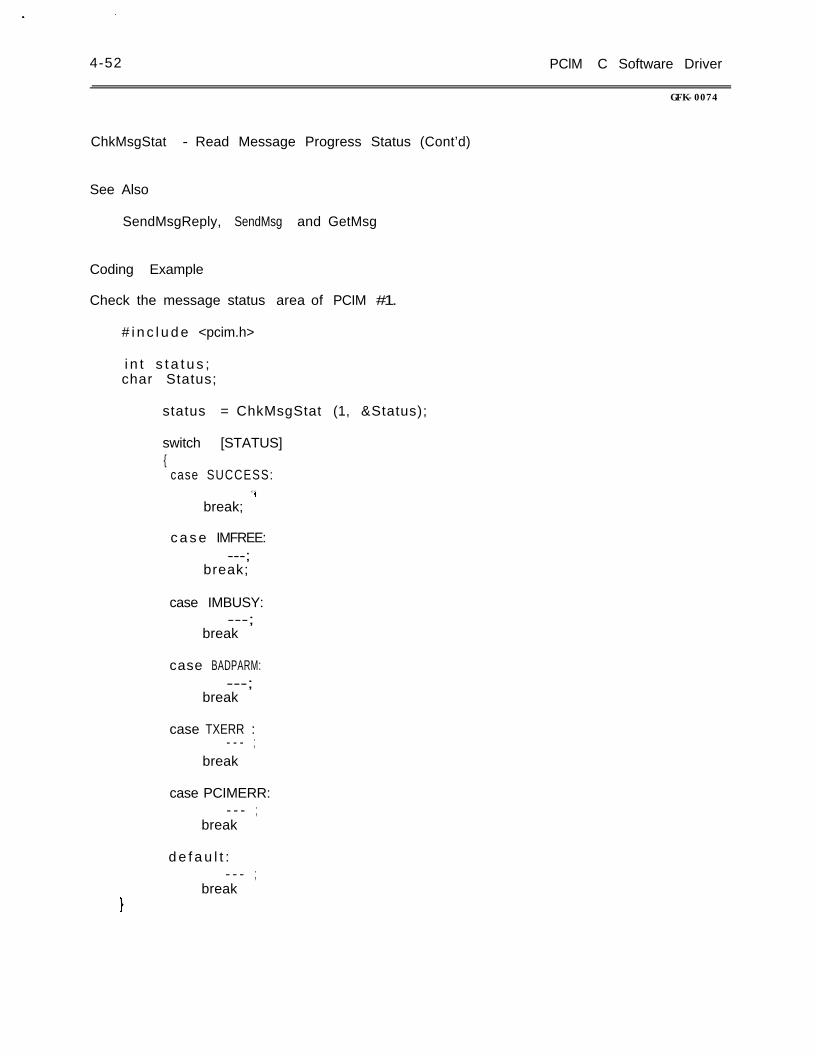
4-52 PClM C Software Driver
GFK-0074
ChkMsgStat - Read Message Progress Status (Cont’d)
See Also
SendMsgReply, SendMsg and GetMsg
Coding Example
Check the message status area of PCIM #1.
# i n c l u d e <pcim.h>
i n t s t a t u s ;char Status;
status = ChkMsgStat (1, &Status);
switch [STATUS]{
case SUCCESS:? ???
break; ’
c a s e IMFREE:---;
break;
case IMBUSY:---;
break
case BADPARM:---;
break
case TXERR :- - - ;
break
case PCIMERR:- - - ;
break
d e f a u l t :- - - ;
break
PCIM C Software Driver 4-53
GFK-0074
GetMsg - Read Received Message
Summary
#include <pcim.h>
intGetMsg (IMnum, Msg)
int IMnum;READ-MESSAGE *Msg;
Description
The Get Message call allows you to read a received memory or non-memory message (ora reply to a previous SendMsgReply call) from the selected PCIM into the Host memory“Msg” parameter.
IMnum is the PClM number configured during initialization. The “Msg” parameter is apointer to the buffer where the received message will be stored.
The format of READ-MESSAGE is:
Source (o-311255 brdcst) - Source address of DeviceFunction code (O-111) - Function CodeSubFunction code (O-255) - Sub Function CodeDE-Indicator (O-134) - D i r e c t e d (1)/Broadcast (0)Length - Data field length/length of messageData (o-134) - Message Data -depends on length parm
Parameters are summarized as follows:
Parameter Values Function- - - - - - - - - - - - - - - - - - - - - - - - - - - - - - - - - - - - - - - - - - - - - - - - - - - - - - - - - - - - - - - - - - - -I Mnum l - 6 4 Relative number of PCIM
Msg see above Pointer to the buffer wherethe received message wi II bestored - see above
GetMsg performs the following sequence:
1) If there is a previous call to SendMsgReply, GetMsg checks to see if thetransmission has successfully completed, and transfers the response back to you.If the response completed with an error, or if in progress, GetMsg will return aFAIL indication.
2) If there is no previous call to SendMsgReply, GetMsg checks to see if there is amemory message, and transfers that message back to you.
4-54 PCIM C Software Driver
GFK-0074
GetMsg - Read Received Message (Cont’d)
3) If no memory messages exist, then GetMsg checks to see if there is a non-memorymessage, and transfers that message back to you.
4) If no messages are present, GetMsg returns with a FAIL status.
NOTE
Unsolicited memory or non-memory Datagrams received by the PCIM may notbe read by the Host while a Send&g/Reply is in progress. This significantlyaffects Host response time to service received Datagrams. lf this is a problem,use the SendMsg call instead of SendMsgReply.
Return Value (Status)
GetMsg will return SUCCESS if a memory or non-memory message is returned to YOU.
Otherwise, one of the following FAIL indications will be returned:
BADIMNUM - IMcount is out of range (a count of 64 or greater).
NOINIT - Indicated PCIM has not been initialized (InitlM).
IMFAIL - The indicated PCIM has failed (PCIM OK = 1).
IMBUSY - The PCIM is otherwise engaged and cannot accept the command.
NOMSG - No message is available to be received at this time.
TXERR - A message transmission has failed.
PCIMERR - There may be a problem with the PCIM firmware.
See Also
SendMsgReply, SendMsg and ChkMsgStat
Coding Example
Check to see if any messages exist on PCIM #1 and if so, store them into the location‘Msg’.
#include <pcim.h>
int status;READ-MESSAGE Msg;
status = GetMsg (1, &Msg);
PCIM C Software Driver 4-55
GFK-0074
GetlNTR - Read Interrupt Status table
Summary
#include <pcim.h>
intGettNTR (IMnum, Intr)
int IMnum;unsigned char *lntr;
Description
The Get Interrupt call allows you to read the selected PCIM’s Interrupt Status Table.You can read this table to:
? see why an interrupt in the Host system has occurred
? report the event in a non-interrupt environment, as is the default state of theSoftware Driver concept (the PCIM will still report the event even though theinterrupt is disabled).
Thus, the Interrupt Status Table can be polled (by reading and interpreting it) todetermine what is interrupting the PCIM. Interrupt conditions are discussed in chapter 3of this manual.
When GetlNTR is called, it transfers the data from the PCIM’s Interrupt Status Table tothe Host memory “lntr” parameter. The format of the Interrupt Status Table and itsassociated macros (shown below) is defined in the summary of data structures in thischapter and in <pcim.h>.
IMnum defines the PClM, as configured during initialization, from which the InterruptStatus Table is to be read. The lntr parameter is a pointer to the buffer where theInterrupt Status Table information is stored.
The format of the lntr table is:
unsigned char Intr[8];
The following Macros are used as shown in the Interrupt Status Table.
Macro Position Explanation
#define I ENABLE 0# d e f i n e IIDISABLE 1
- E n a b l e t h e i n t e r r u p t l e v e l .- Disable the interrupt level.
#define I SUMMARY 0#define I - R E Q U E S T 0 1#define I - P C I M STAT 2#define I_DEV STAT 3#define I - O U T - S E N T 4#define I-CCMPLETE 5#define IIRECE IVE-D 6
- Summary if interrupt occurred.- Received memory datagram.- PCIM Status Change - usually fatal.- Device Status Change.- Outputs sent - end of bus access.- Command Block completed.- Received Datagram.

4-56 PCIM C Software Driver*
GFK-0074
GetlNTR - Read Interrupt Status Table (Cont’d)
After data transfer to the Host is complete, GetlNTR clears all of the PCIM’s InterruptStatus Table bytes each time it is called, This way, you can see the lastest event that hasoccurred each call.
Parameters are summarized as follows:
Parameter Va I ues function-------------------------------------------------------------------------IIMnLml l-64 Relative number of PClM
l n t r see above Pointer to the buffer wherethe table data will be stored
Return Value (Status)
GetlNTR will return SUCCESS if the device specified by IMnum is present on the serialbus. If the target device is not present, or is out of range, GetlNTR will return FAIL.The following FAIL indications will be returned:
BAD I MNUM - IMcount is out of range (a count of 64 or greater).
NOINIT - Indicated PCIM has not been initialized (InitlM).
IMFAIL - The indicated PClM has fai led (PCIM OK = 1).
Coding Example
This example shows how, if an interrupt occurs on PClM #1, to transfer the contents ofthat PCIM’s Status Table. Interpretation of bits will depend on which interrupt isEnabled, and which application is to be run.
#include <pcim.h>
i n t s t a t u s ;unsigned char Intr[8];
i f ((status = GetlNTR (1, Intr)) !=SUCCESS)report=err (1, s t a t u s ) ;
else[ /*do what’s necessary for interrupt processing*/I

PCIM C Software Driver 4-57P
GFK-0074
PutlNTR - Write to the Interrupt Disable Table
Summary
#include <pcim.h>
intPutlNTR (IMnum, Disablelntr)
int IMnum;unsigned char *Disablelntr;
Description
The Put Interrupt call allows you to write to the selected PClM’s Interrupt DisableTable. The PutlNTR call first initializes a table to Enable and Disable individualinterrupts as you require. The PutlNTR call then writes this table to the InterruptDisable Table on the PCIM. You can Enable or Disable interrupts in any mix; that is, on asingle call, some interrupts may be Enabled and some Disabled, all may be Enabled, or allof the interrupts may be Disabled. Interrupt conditions are discussed in chapter 3 of thismanua I.
When PutlNTR is called, it transfers the data from the Host memory “Disablelntr”parameter to the PCIM’s Interrupt Disable Table. The format of the Interrupt DisableTable and its associated macros (shown below) is defined in the summary of datastructures in this chapter and in <pcim.h>.
IMnum defines the PCIM, as configured during initialization, to which Disabletntr will be.I The Disablelntr parameter is a pointer to the buffer where the Interrupt Disable
A;Dle information is stored.
The format of the Disablelntr table is:
unsigned char Disablelntr[B];
The following Macros are used as shown in the Interrupt Disable Table.
Macro Position Explanation
#define I ENABLE 0# d e f i n e I_DISABLE 1
- Enable the interrupt level.- Disable the interrupt level.
#define I SUMMARY 0#def i ne I-REQUEST Q 1# d e f i n e I PCIM STAT 2# d e f i n e I DEV STAT 3# d e f i n e I_OUT_SENT 4# d e f i n e I CCOMPLETE 5# d e f i n e I_RECEIVE-D 6
- Summary if interrupt occurred.- Received memory datagram.- PCIM Status Change - usually fatal.- Device Status Change.- Outputs sent - end of bus access.- Command Block completed.- Received Datagram.

4-58 PCIIM C Software Driver
GfK-0074
PutlNTR - Write to the Interrupt Disable Table (Cont’d)
Parameters are summarized as follows:
Parameter Values Function--------------------------------------------------------------------I Mnum l-64 Relative number of PCIM
D i s a b l e l n t r see above Pointer to the buffer fromwhich enable/disable data is sent
Return Value (Status)
PutlNTR will return SUCCESS if the device specified by IMnum is present on the serialbus. If the target device is not present, or is out of range, Putlntr will return FAIL. Thefollowing FAIL indications will be returned:
BADIMNUM - IMcount is out of range (a count of 64 or greater).
NOINIT - Indicated PCIM has not been initialized (InitlM).
IMFAIL - The indicated PCIM has failed (PCIM OK = 1).
Coding Example
This example enables the Receive Datagram interrupt.
#include <pcim.h>
i n t s t a t u s ;*
unsigned c h a r Disablelntr[8];
/* Initialize the Disable Table*/f o r (x = 0; x < 8; xtt)
Disablelntr [ x ] = I-DISABLE /* D i s a b l e a l l I n t e r r u p t s * /
/*Enable Receive Datagram Interrupt*/Disablelntr [I_RECEIVE_D] = J-ENABLE;
/*Now call use the call*/i f ( ( s t a t u s = Put\NTR (1, Disablelntr )) != SUCCESS)
report=err ( 1 , s t a t u s ) ;
PCIM BASIC Software Driver 4-59
GFK-0074
SECTION BBASIC LANGUAGE PCIM SOFTWARE DRIVER
Basic Software Driver Installation
The Basic Software Driver function call subroutines are made resident in your systemwhen you execute the Driver code file once under MS/DOS as follows:
1) Type 'PCIMX’ in response to the DOS prompt ‘A>‘.
- The Driver code file is loaded into memory.
- A short initialization sequence inside the Driver is executed.
2) The Driver code displays the message ‘PCIM Drivers Version x.x are Resident’ andexits to DOS.
- The Driver is resident in memory and available for use.
- BASICA or GWBASIC can be loaded and calls to the Drivers performed.
If you need to recover the memory space occupied by the Driver, you must perform asystem reset. In most cases, this will not be necessary since Driver code occupies only asmall amount of memory (13K). If you plan to access the Driver frequently, the Drivercode f i l e c a n b e m o v e d t o y o u r system disk and executed from inside yourAUTOEXEC.BAT file at startup. This will automatically make the Driver resident.
Basic Software Driver Function Call Parameters
Software Driver function calls require that you specify a number of parameters for eachcall. The data structures for each parameter, which are linked and loaded from theSoftware Driver .exe file, are summarized below.
IBM PC BASICA interpreter does not allow the passing of constants in the parameter listof a CALL statement. Only variables may be passed. You must load all variables whichsupply information to the Driver before performing a function call. In the parameter listswhich follow, all parameters are either single integers or are arrays of integers.
NOTE
BASICA interpreter r e q u i r e s t h a t a l l a r r a y s b e c a l l e d w i t hsubscript. If this is violated, incorrect data and/or system crash isthe usual result.
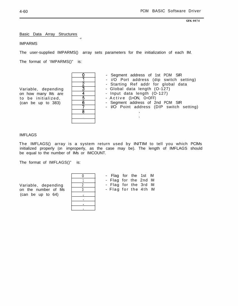
4-60 PCIM BASIC Software Driver
GFK-0074
Basic Data Array Structures-+
IMPARMS
The user-supplied IMPARMS() array sets parameters for the initialization of each IM.
The format of ‘IMPARMS()” is:
Variable, dependingon how many IMs aret o b e i n i t i a l i z e d ,(can be up to 383)
.
- Segment address of 1st PCIM SIR- i/O Port address (dip switch setting)- Starting Ref addr for global data- Global data length (O-127)- Input data length (O-127)- A c t i v e (1=ON, O=OFF)- Segment address of 2nd PCIM SIR- I/O Point address (DIP switch setting)
IMFLAGS
The IMFLAGS() array is a system return used by INITIM to tell you which PClMsinitialized properly (on improperly, as the case may be). The length of IMFLAGS shouldbe equal to the number of IMs or IMCOUNT.
The format of IMFLAGS()” is:
Variable, dependingon the number of IMs(can be up to 64)
0 - Flag for the 1st IM1 - Flag for the 2nd IM2 - Flag for the 3rd IM3 - F l a g f o r t h e 4 t h IM
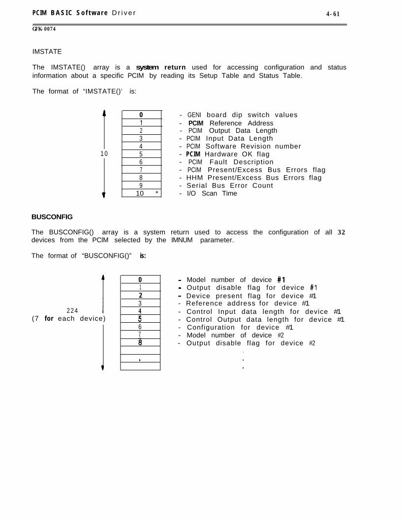
PCIM B A S I C S o f t w a r e D r i v e r
GFK-0074
4-61
IMSTATE
The IMSTATE() array is a system return used for accessing configuration and statusinformation about a specific PCIM by reading its Setup Table and Status Table.
The format of “IMSTATE()’ is:
1 0
0 - GENI board dip switch values1 - PCIM Reference Address23
- PCIM Output Data Length
4- PCIM Input Data Length- PCIM Software Revision number
56
- PCIM Hardware OK flag- PCIM Fault Description
78
- PCIM Present/Excess Bus Errors flag
9- HHM Present/Excess Bus Errors flag- Serial Bus Error Count
10 * - I/O Scan Time
BUSCONFIG
The BUSCONFIG() array is a system return used to access the configuration of all 32devices from the PClM selected by the IMNUM parameter.
The format of “BUSCONFIG()” is:
2 2 4 I(7 for each device)
01234i67s.
- Model number of device #l- Output disable flag for device #I- Device present f lag for device #1- Reference address for device #1- Control Input data length for device #1- Control Output data length for device #1- Configuration for device #1- Model number of device #2- Output disable f lag for device #2
.
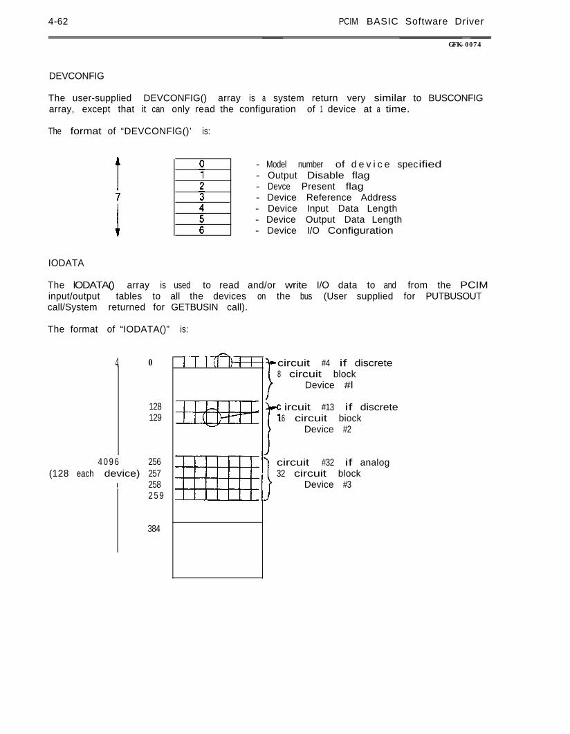
4-62 PCIM BASIC Software Driver
GFK-0074
DEVCONFIG
The user-supplied DEVCONFIG() array is a system return very similar to BUSCONFIGarray, except that it can only read the configuration of 1 device at a time.
The format of “DEVCONFlG()’ is:
IODATA
- Model number of d e v i c e spec- Output Disable flag- Devce Present flag- Device Reference Address- Device Input Data Length- Device Output Data Length- Device I/O Configuration
ified
The lODATA() array is used to read and/or write I/O data to and from the PCIMinput/output tables to all the devices on the bus (User supplied for PUTBUSOUTcall/System returned for GETBUSIN call).
The format of “IODATA()” is:
4 0
128129
4 0 9 6 256(128 each device) 257
I 2582 5 9
384
-IIMD; i circuit #4 if discrete
8 circuit blockDevice #l
F
ircuit #13 if discrete16 circuit biock
Device #2
circuit #32 if analog32 circuit block
Device #3
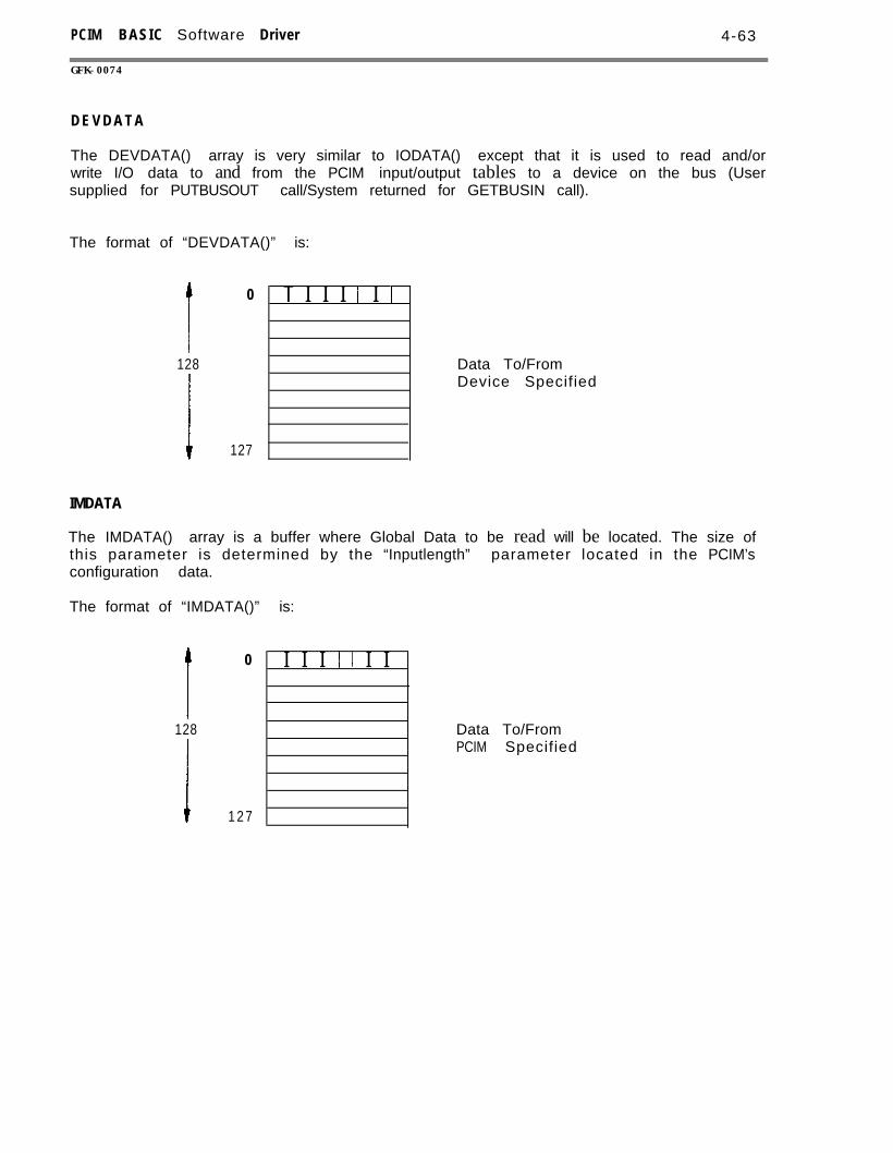
PCIM BASIC Software Driver 4-63
GFK-0074
D E V D A T A
The DEVDATA() array is very similar to IODATA() except that it is used to read and/orwrite I/O data to and from the PCIM input/output tables to a device on the bus (Usersupplied for PUTBUSOUT call/System returned for GETBUSIN call).
The format of “DEVDATA()” is:
I 0
128
I 127
T I I I I I I
Data To/FromDevice Specified
IMDATA
The IMDATA() array is a buffer where Global Data to be read will be located. The size ofthis parameter is determined by the “Inputlength” parameter located in the PCIM’sconfiguration data.
The format of “IMDATA()” is:
I 0
128
1 1 2 7
I I I I I I I
Data To/FromPCIM Specified

4-64 PCIM BASIC Software Driver
GFK-0074
M S G
The MSG() array is a buffer where the message to be sent (SENDMSG) or message to bereceived (GETMSG) will be stored.
The format of “MSG()” is:
INTR/DISABLEINTR
The INTR and DtSABLEINTR arrays are used to read the selected PCIM’s Interrupt StatusTable and write to the selected PCIM’s Interrupt Disable Table, respectively.
The format of “INTR” and DISABLElNTR” is:
t7
01234i6
- Summary if interrupt occurred- Received Memory Datagram- PCIM Status Change - usually fatal- Device Status Change- Outputs sent - end of bus access- Command Block completed- Received Datagram
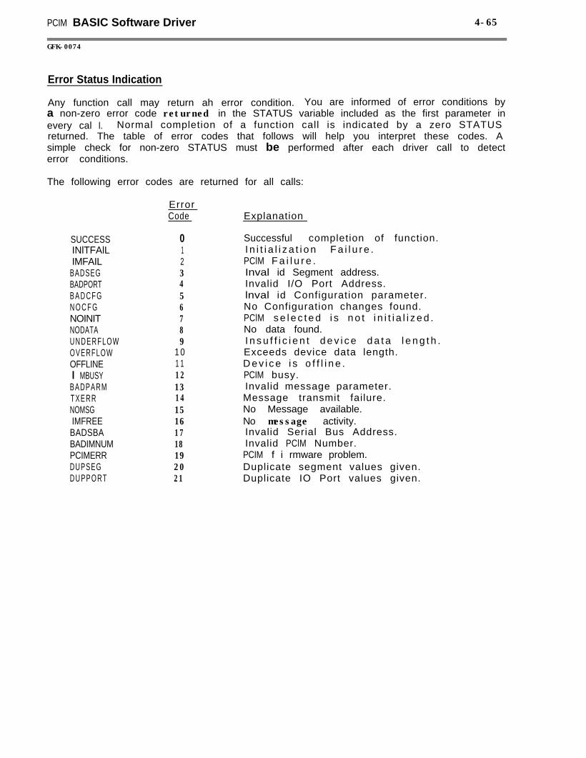
PCIM BASIC Software Driver 4-65
GFK-0074
Error Status Indication
Any function call may return ah error condition. You are informed of error conditions bya non-zero error code returned in the STATUS variable included as the first parameter inevery cal I. Normal completion of a function call is indicated by a zero STATUSreturned. The table of error codes that follows will help you interpret these codes. Asimple check for non-zero STATUS must be performed after each driver call to detecterror conditions.
The following error codes are returned for all calls:
ErrorCode Explanation
SUCCESSINlTFAlLIMFAIL
BADSEGBADPORTB A D C F GN O C F GNOINITNODATAU N D E R F L O WOVERFLOWOFFLINEI MBUSY
BADPARMTXERRNOMSGIMFREEBADSBABADIMNUMPCIMERRDUPSEGDUPPORT
0 Successful completion of function.1 I n i t i a l i z a t i o n F a i l u r e .2 PClM F a i l u r e .3 Inval id Segment address.4 Invalid I/O Port Address.5 lnval id Configuration parameter.6 No Configuration changes found.7 PClM s e l e c t e d i s n o t i n i t i a l i z e d .8 No data found.9 I n s u f f i c i e n t d e v i c e d a t a l e n g t h .
1 0 Exceeds device data length.1 1 D e v i c e i s o f f l i n e .12 PCIM busy.13 Invalid message parameter.14 Message transmit failure.15 No Message available.16 No message activity.17 Invalid Serial Bus Address.18 Invalid PClM Number.19 PCIM f i rmware problem.20 Duplicate segment values given.21 Duplicate IO Port values given.
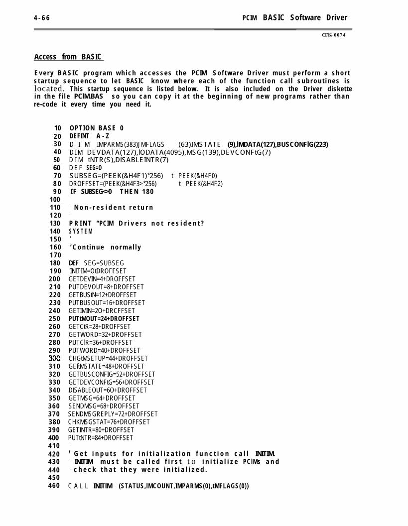
4 - 6 6 PCIM BASIC Software Driver
CFK-0074
Access from BASIC
E v e r y B A S I C p r o g r a m w h i c h a c c e s s e s t h e PCIM S o f t w a r e D r i v e r m u s t p e r f o r m a s h o r ts t a r t u p s e q u e n c e t o l e t BASIC k n o w w h e r e e a c h o f t h e f u n c t i o n c a l l s u b r o u t i n e s i slocated. This startup sequence is listed below. It is also included on the Driver diskettei n t h e f i l e PClM.BAS s o y o u c a n c o p y i t a t t h e b e g i n n i n g o f n e w p r o g r a m s r a t h e r t h a nre-code it every time you need it.
102 03 04 050607 08 09 0
1001101 2 01301401 5 01 6 01 7 01801 9 02 0 02 1 02 2 02 3 02 4 02 5 02 6 02 7 02 8 02 9 0
3 1 03 2 03 3 03 4 03 5 03 6 03 7 03 8 03 9 04004 1 04 2 04 3 04 4 04 5 04 6 0
OPTION BASE 0DEFINT A - ZD I M IMPARMS(383)JMFLAGS (63)IMSTATE (9),lMDATA(127),BUSCONFlG(223)D I M DEVDATA(127),lODATA(4095),MSG(139),DEVCONFtG(7)D I M tNTR(S),DlSABLEINTR(7)D E F SEG=OSUBSEG=(PEEK(&H4F1)*256) t PEEK(&H4F0)DROFFSET=(PEEK(&H4F3>*256) t PEEK(&H4F2)I F SUBSEG<>0 T H E N 1 8 0I
’ N o n - r e s i d e n t r e t u r nI
P R I N T “PCIM D r i v e r s n o t r e s i d e n t ?S Y S T E M1
‘ C o n t i n u e n o r m a l l y
DEF SEG=SUBSEGINITIM=OtDROFFSETGETDEVIN=4+DROFFSETPUTDEVOUT=8+DROFFSETGETBUStN=12+DROFFSETPUTBUSOUT=16+DROFFSETGETIMIN=2O+DRCFFSETPUTtMOUT=24+DROFFSETGETCtR=28+DROFFSETGETWORD=32+DROFFSETPUTClR=36+DROFFSETPUTWORD=40+DROFFSETCHGtMSETUP=44+DROFFSETGEftMSTATE=48+DROFFSETGETBUSCONFIG=52+DROFFSETGETDEVCONFtG=56+DROFFSETDISABLEOUT=6O+DROFFSETGETMSG=64+DROFFSETSENDMSG=68+DROFFSETSENDMSGREPLY=72+DROFFSETCHKMSGSTAT=76+DROFFSETGETINTR=80+DROFFSETPUTtNTR=84+DROFFSET1
’ G e t i n p u t s f o r i n i t i a l i z a t i o n f u n c t i o n c a l l INITIM.’ INITIM m u s t b e c a l l e d f i r s t t o i n i t i a l i z e PClMs a n d’ c h e c k t h a t t h e y w e r e i n i t i a l i z e d .
C A L L INITlM (STATUS,lMCOUNT,IMPARMS(0),tMFLAGS(0))
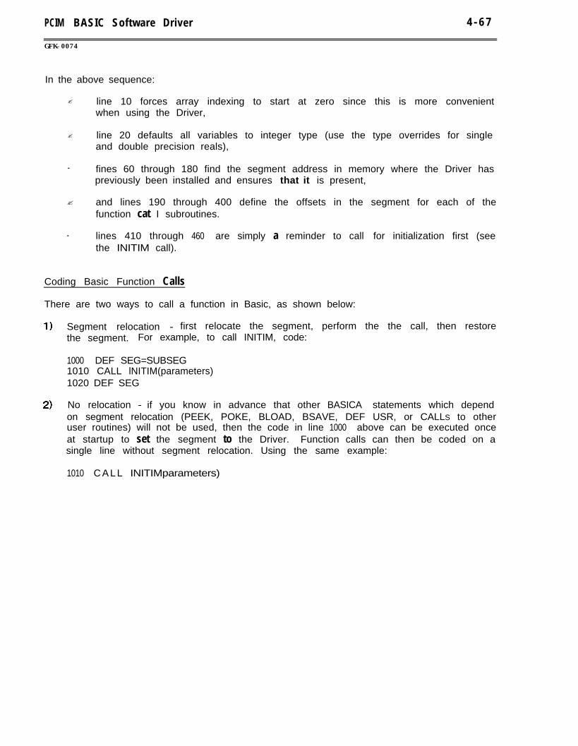
PCIM BASIC Software Driver 4 - 6 7
GFK-0074
In the above sequence:
? line 10 forces array indexing to start at zero since this is more convenientwhen using the Driver,
? line 20 defaults all variables to integer type (use the type overrides for singleand double precision reals),
- fines 60 through 180 find the segment address in memory where the Driver haspreviously been installed and ensures that it is present,
? and lines 190 through 400 define the offsets in the segment for each of thefunction cat I subroutines.
- lines 410 through 460 are simply a reminder to call for initialization first (seethe INITIM call).
Coding Basic Function Calls
There are two ways to call a function in Basic, as shown below:
Segment relocation - first relocate the segment, perform the the call, then restorethe segment. For example, to call INITIM, code:
1000 DEF SEG=SUBSEG1010 CALL lNITIM(parameters)1020 DEF SEG
No relocation - if you know in advance that other BASICA statements which dependon segment relocation (PEEK, POKE, BLOAD, BSAVE, DEF USR, or CALLS to otheruser routines) will not be used, then the code in line 1000 above can be executed onceat startup to set the segment to the Driver. Function calls can then be coded on asingle line without segment relocation. Using the same example:
1010 C A L L INITIMparameters)
4-68 PCIM BASIC Software Driver
GFK-0074
Basic Software Driver Function Call Presentation
This section provides a sample of the format and notation in which individual functioncalls are presented in Basic. Individual function calls are discussed in the pages thatfollow. The presentation format for function calls is:
CALL NAME CALL Statement
- Syntax
CALL NAME (STATUS, Parameter List)
a Act ion
A brief statement of the call’s function.
- Remarks
A detailed description of the function call; including a description of the function, asummary of the function’s action sequence, and a summary of the parameters used in thecall.
A parameter format listing for parms described for the first time (as shown in quotes inthe text) is included for each call. If a parameter is complex, this information will berepeated for each using call. If containing only one field, format may not be shown.
- Status Value
A detailed description of status values and their meanings.
a Coding Example
A description of a generic application, and sample coding using the call.
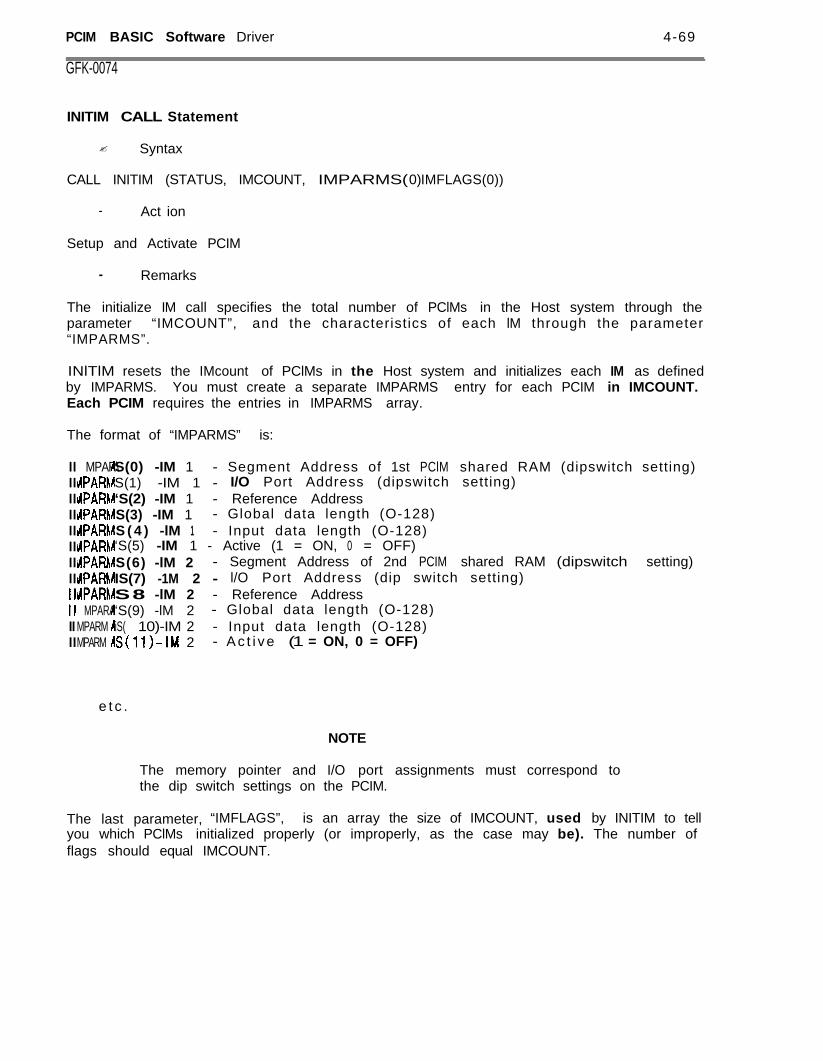
PCIM BASIC Software Driver 4-69
GFK-0074
INITIM CALL Statement
? Syntax
CALL INITIM (STATUS, IMCOUNT, IMPARMS(0) IMFLAGS(0))
- Act ion
Setup and Activate PCIM
- Remarks
The initialize IM call specifies the total number of PClMs in the Host system through theparameter “IMCOUNT”, and the characteristics of each lM through the parameter“IMPARMS”.
INlTlM resets the IMcount of PClMs in the Host system and initializes each IM as definedby IMPARMS. You must create a separate IMPARMS entry for each PCIM in IMCOUNT.Each PCIM requires the entries in IMPARMS array.
The format of “IMPARMS” is:
II MPAR\IIrlPAR1IIdPARAIIrlPARhIItiPARhIIrAPARhIItiPAR)IIIdPAmII MPAR),II MPARAII MPARMIIMPARM
S(0) -IM 1 - Segment Address of 1st PClM shared RAM (dipswitch setting)S(1) -IM 1 - I/O Port Address (dipswitch setting)‘S(2) -IM 1 - Reference AddressS(3) -IM 1 - Global data length (O-128)S ( 4 ) -lM 1 - Input data length (O-128)‘S(5) -IM 1 - Active (1 = ON, 0 = OFF)S(6) -lM 2 - Segment Address of 2nd PCIM shared RAM (dipswitch setting)IS(7) -1M 2 - l/O Port Address (dip switch setting)S8 -lM 2 - Reference Address‘S(9) -lM 2 - Global data length (O-128)iS( 10)-IM 2 - Input data length (O-128)(S-IM 2 - A c t i v e (1 = ON, 0 = OFF)
e t c .
NOTE
The memory pointer and I/O port assignments must correspond tothe dip switch settings on the PCIM.
The last parameter, “IMFLAGS”, is an array the size of IMCOUNT, used by INITIM to tellyou which PClMs initialized properly (or improperly, as the case may be). The number offlags should equal IMCOUNT.
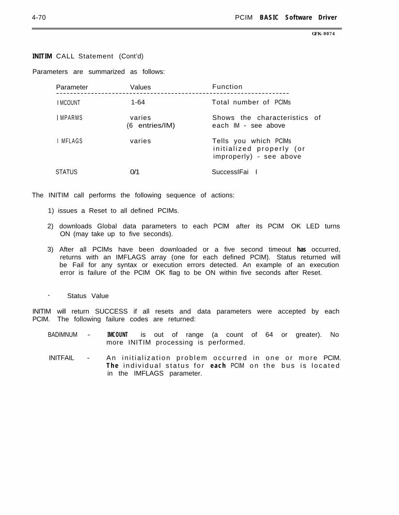
4-70 PCIM BASIC Software Driver
GFK-0074
INITIM CALL Statement (Cont’d)
Parameters are summarized as follows:
Parameter Values Function-------------------------------------------------------------------I MCOUNT 1-64 Total number of PClMs
i MPARMS varies(6 entries/IM)
Shows the characteristics ofeach IM - see above
I MFLAGS varies Tells you which PClMsi n i t i a l i z e d p r o p e r l y ( o rimproperly) - see above
STATUS 0/1 SuccessIFai I
The INITIM call performs the following sequence of actions:
1) issues a Reset to all defined PCIMs.
2) downloads Global data parameters to each PClM after its PCIM OK LED turnsON (may take up to five seconds).
3) After all PClMs have been downloaded or a five second timeout has occurred,returns with an IMFLAGS array (one for each defined PCIM). Status returned willbe Fail for any syntax or execution errors detected. An example of an executionerror is failure of the PCIM OK flag to be ON within five seconds after Reset.
- Status Value
INITIM will return SUCCESS if all resets and data parameters were accepted by eachPCIM. The following failure codes are returned:
BADIMNUM - IMCOUNT is out of range (a count of 64 or greater). Nomore INITIM processing is performed.
INITFAIL - A n i n i t i a l i z a t i o n p r o b l e m o c c u r r e d i n o n e o r m o r e PCIM.T h e i n d i v i d u a l s t a t u s f o r e a c h PCIM o n t h e b u s i s l o c a t e din the IMFLAGS parameter.
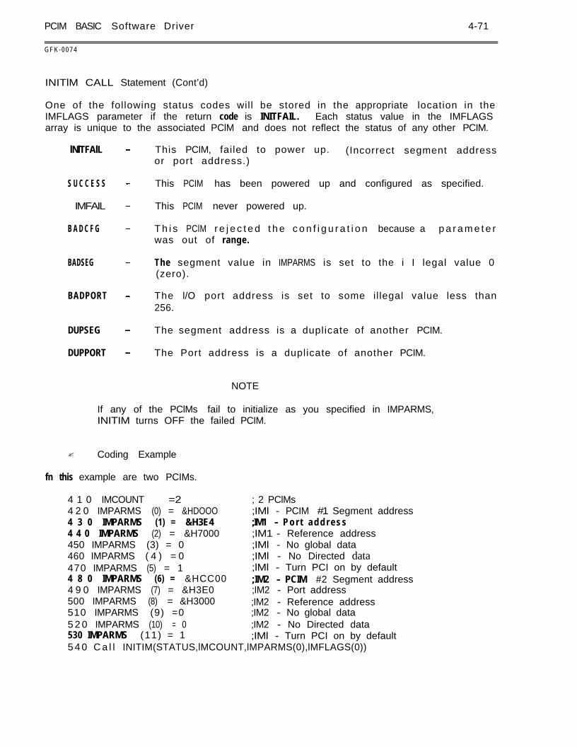
PCIM BASIC Software Driver 4-71
G F K - 0 0 7 4
INITlM CALL Statement (Cont’d)
One of the following status codes will be stored in the appropriate location in theIMFLAGS parameter if the return code is INITFAIL. Each status value in the IMFLAGSarray is unique to the associated PClM and does not reflect the status of any other PCIM.
lNlTFAlL
S U C C E S S
IMFAIL
B A D C F G
BADSEG
BADPORT
DUPSEG
DUPPORT
This PCIM, failed to power up. (Incorrect segment addressor port address.)
This PCIM has been powered up and configured as specified.
This PCIM never powered up.
T h i s PClM r e j e c t e d t h e c o n f i g u r a t i o n because a p a r a m e t e rwas out of range.
The segment value in IMPARMS is set to the i I legal value 0(zero).
The l/O port address is set to some il legal value less than256.
The segment address is a duplicate of another PCIM.
The Port address is a duplicate of another PCIM.
NOTE
If any of the PClMs fail to initialize as you specified in IMPARMS,INITIM turns OFF the failed PCIM.
? Coding Example
fn this example are two PCIMs.
4 1 0 IMCOUNT =2 ; 2 PClMs4 2 0 IMPARMS (0) = &HDOOO ;IMl - PCIM #1 Segment address4 3 0 IMPARMS (1) = &H3E4 ;IM1 - P o r t a d d r e s s4 4 0 IMPARMS (2) = &H7000 ;IM1 - Reference address450 IMPARMS (3) = 0 ;IMl - No global data460 IMPARMS ( 4 ) = 0 ;IMl - No Directed data470 IMPARMS (5) = 1 ;lMl - Turn PCI on by default4 8 0 IMPARMS (6) = &HCC00 ;IM2 - PCIM #2 Segment address4 9 0 IMPARMS (7) = &H3E0 ;IM2 - Port address500 IMPARMS (8) = &H3000 ;IM2 - Reference address510 IMPARMS (9) =0 ;IM2 - No global data5 2 0 IMPARMS (10) = 0 ;IM2 - No Directed data530 IMPARMS (11) = 1 ;IMl - Turn PCI on by default5 4 0 C a l l INITIM(STATUS,lMCOUNT,lMPARMS(0),lMFLAGS(0))
4-72 PCIM BASIC Software Driver
G F K - 0 0 7 4
CHGIMSETUP CALL Statement
- Syntax
CALL CHGIMSETUP (STATUS, IMNUM, IMPARMS(0))
- Action
Change PClM Configuration
- Remarks
Following initialization, any changes you make to the configuration of a specific PClMmust use the Change IM Setup call. This call allows you to make configuration changes toa specific PClM Setup Table by writing the IMPARMS parameter from Host memory to it.
The IMMNUM” parameter i s a n o f f s e t o f t h e lMPARMS p a r a m e t e r w h i c h , a f t e rinitialization, indicates the specific PClM in the host system for which configurationchanges are intended. The relative IMNUM cannot itself be changed.
NOTE
Configuration changes to any PCIM while online causes that IM tostop transmitting on the serial bus for 1.5 seconds.
The format of “IMPARMS” is the same as shown in the INlTlM call. However only four oft h e parame
IMPARMS(IMPARMS(IMPARMS(IMPARM(
ters should be allowed to be changed. These are as follows:
+2) - Reference Address+3) - Global data length+4) - Input data length+S) - Active (1 = ON, 0 = OFF)
I = (IMNUM-I)*6
Parameters are summarized as follows:
Parameter Va I ues Function- - - - - - - - - - - - - - - - - - - - - - - - - - - - - - - - - - - - - - - - - - - - - - - - - - - - - - - - - - - - - - - - - - - -I MNUM 1-64 Relative number of PCIM
I MPARMS varies Shows the characteristics ofe a c h IM - see above
STATUS 0/1 Success/Faill I
PCIM BASIC Software Driver 4-73
CFK-0074
CHGIMSETUP CALL Statement (Cont’d)
- Status Value
CHGIMSETUP will return SUCCESS if all changes were accepted by the target IM. If theIM fails to change to the new parameters, the following FAIL indications will be returned:
BADIMNUM - lnval id PCIM number.
NOINIT - Indicated PCIM has not been initialized (INITIM).
IMFAIL - T h e i n d i c a t e d PCIM h a s f a i l e d (PCIM O K = 1), o r n e v e rcompleted processing the config change command.
IMBUSY - The PCIM is otherwise engaged and cannot accept the configchange command.
BADCFG - This PCIM rejected the configuration because a parameterwas out of range.
NOCFG - T h e PCIM, a f t e r e x a m i n i n g t h e r e c e i v e d t h e config c h a n g ecommand, found no changes to make.
INITFAIL - The PCIM failed to power up.
? Coding Example
Change the reference address for PCIM #1.
600 IMNUM =1610 IMPARMS (2) = &H6000 ;new reference address620 Call CHGIMSETUP(STATUS, IMNUM, IMPARMS(0))
Turn off PCIM #2,
690 IMNUM = 2700 IMPARMS (2) = &H7500720 Call CHGlMSETUP(STATUS,IMNUM,IMPARMS(0))7 3 0 ‘Check status for next action7 4 0 If STATUS = 0 Then 760 else 800
4 - 7 4 PCIM B A S I C Software D r i v e r
GFK-0074
GETIMSTATE CALL Statement
- Syntax
CALL GETIMSTATE (STATUS, IMNUM, IMSTATE(0))
- Act ion
Get Configuration and Status Information
- Remarks
The Get IM State call allows you to access configuration and status information about aspecific PClM by reading its Setup Table and Status Table into the “IMSTATE” parameterin iiost memory.
The format of IMSTATE is:
IMSTATE(0) DipSwitch - GENI Daughterboard Dip Switch ValueIMSTATE(1) IMRef - Reference AddressIMSTATE(2) OutputLength - Output Control Data LengthIMSTATE(3) InputLength - input Control Data LengthIMSTATE(4) Revision - PCIM Firmware Revision NumberIMSTATE(5) PCIM OK - PCIM OK = 0 - every 200 ms, set to ‘1’IMSTATE(6) F a u l t - O v e r a l l f a u l t b y t e - a n y PCIM f a u l tIMSTATE(7) A c t i v e - Hand Held Monitor PresentIMSTATE(8) SBerr - Serial Bus error countIMSTATE(9) ScanTime - B u s S c a n T i m e in ms
Before returning, GETIMSTATE will also clear the PCIM OK flag of the selected PCIM.Since the PCIM periodically sets its PCIM OK flag, this cal I allows the implementation ofa PCIM OK heartbeat procedure.
Parameters are summarized as fol fows:
Parameter V a l u e s F u n c t i o n-----------------------------------------------------------------
IIMNUM l - 6 4 Relative number of PCIM
IMSTATE varies PCIM Configuration andStatus -see above
STATUS 0/1 Success/Fail
PCIM BASIC Software Driver 4-75
GFK-0074
GETIMSTATE CALL Statement (Cont’d)
? Status value
GETIMSTATE will almost always return SUCCESS. If the target IM is currently offline,has not been initialized, or is out of range, the following FAIL indications will be returned:
BAD I MNUM - IMCOUNT is out of range (a count of 64 or greater).
NOINIT - indicated PCIM has not been initialized (INITIM).
IMFAIL - The indicated PCIM has failed (PCIM OK = 1).
? Coding Example
Examine the state of PCIM #1.
1000 lMNUM=11010 C A L L GETlMSTATE(STATUS,IMNUM,lMSTATE(0))

4-76 PClM BASIC Software Driver
GFK-0074
GETBUSCONFIG CALL Statement
- Syntax
CALL GETBUSCONFIG (STATUS, IMNUM, MJSCONFlG(0))
a Act ion
Get Serial Bus Configuration
a Remarks
The Get Bus Configuration call allows you to read device configuration information aboutall devices on a serial bus. GETBUSCONFIG reads all 32 Device Configuration Tablesfrom the PCIM selected by IMNUM into the Host memory “BUSCONFIG” parameter.BUSCONFIG parm - 224 in length, 7 entries per device.
The format of BUSCONFIG is:
BUSCONFIG (0) ModelBUSCONFIG (1) OutputDisableBUSCONGIG (2) PresentBUSCONFIG (3) Reference
BUSCONFIG (4) InputLengthBUSCONFIG (5) OutputlengthBUSCONF I G (6) Con f i g
Not UsedDevice Conf ig
Parameters are summarized as follows:
Parameter Values
- Model Number of device- Output disable flag- Device Present flag- Status Table or
Reference Address- Control Input Data Length- Control Output Data Length- Device Configuration
1 = al I inputs2 = all outputs3 = combination---------c----------___3_______
1716l~14l31211101--c-----------------______I____
I I I I I I I Icc------------------____I_ 1 I
Function--------------------------------------------------------------------I MNUM 1-64 Relative number of PCIM
BUSCONF I G 224 entries Device configuration(7 entries/device) information about all
devices on a serial bus- see above
STATUS 0/1 Success/Fail

PCIM B A S I C S o f t w a r e D r i v e r 4-77
GFK-0074
G E T B U S C O N F I G C A L L S t a t e m e n t (Cont’d)
- Status Value
GETBUSCONFIG will almost always return SUCCESS. If the target IM is currentlyoffline, has not been initialized, or is out of range, the following FAIL indications will bereturned:
BADIMNUM - IMCOUNT is out of range (a count of 64 or greater).
NOINIT - Indicated PCIM has not been initialized (INITIM).
IMFAIL - The indicated PCIM has failed (PCIM OK = 1).
O F F L I N E - N o n e o f t h e d e v i c e s s p e c i f i e d a r e c u r r e n t l y a c t i v e o n t h ebus. However , the appropriate buffer is st i I I returned andw i I I c o n t a i n c o n f i g u r a t i o n d a t a f o r d e v i c e s o n c ei n .
I oggedZeros wi I I be returned if no device has logged in to a
p a r t i c u l a r s l o t .
? Coding Example
Examine the configuration of the devices on PCIM #1.
1 1 0 0 IMNUM = 11 1 1 0 Call GETBUSCONFIG (STATUS,lMNUM,BUSCONFIG(0))
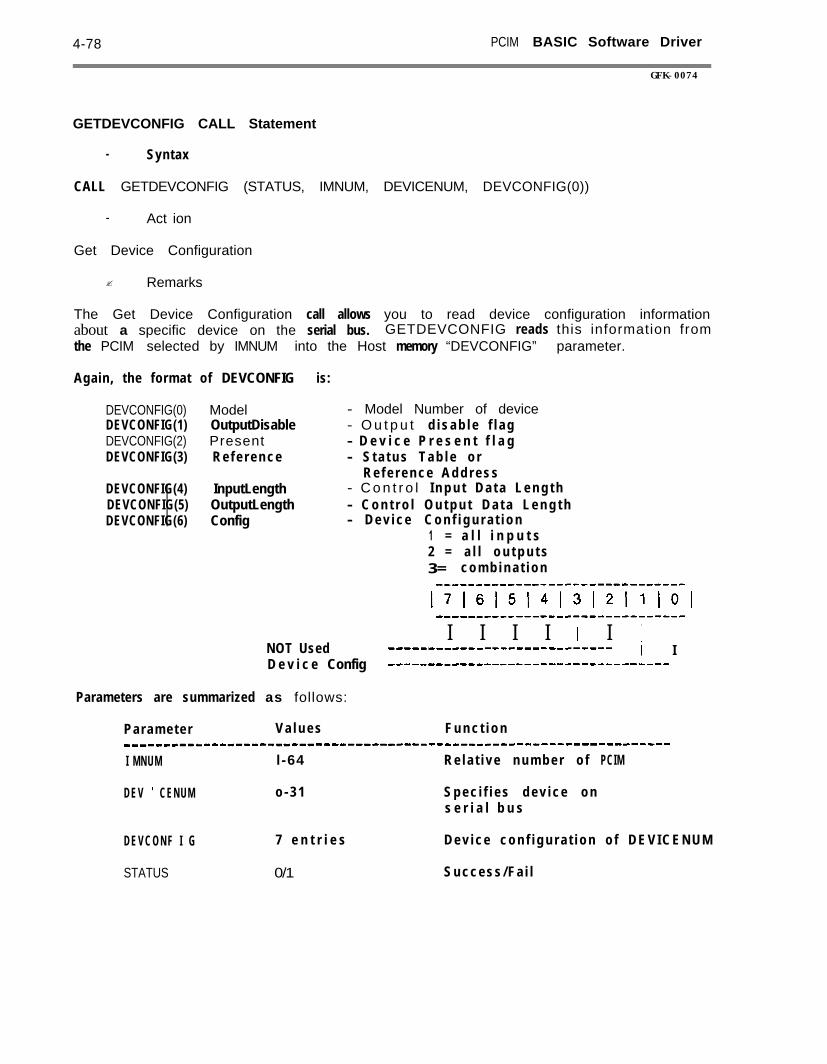
4-78 PCIM BASIC Software Driver
GFK-0074
GETDEVCONFIG CALL Statement
- Syntax
CALL GETDEVCONFIG (STATUS, IMNUM, DEVICENUM, DEVCONFIG(0))
- Act ion
Get Device Configuration
? Remarks
The Get Device Configuration call allows you to read device configuration informationabout a specific device on the serial bus. GETDEVCONFIG reads this information fromthe PCIM selected by IMNUM into the Host memory “DEVCONFIG” parameter.
Again, the format of DEVCONFIG is:
DEVCONFIG(0) Model - Model Number of deviceDEVCONFIG(1) OutputDisable - O u t p u t d i s a b l e f l a gDEVCONFIG(2) Present - D e v i c e P r e s e n t f l a gDEVCONFIG(3) R e f e r e n c e - S t a t u s T a b l e o r
R e f e r e n c e A d d r e s sDEVCONFIG(4) InputLength - C o n t r o l I n p u t D a t a L e n g t hDEVCONFIG(5) OutputLength - C o n t r o l O u t p u t D a t a L e n g t hDEVCONFIG(6) Config - D e v i c e C o n f i g u r a t i o n
1 = a l l i n p u t s2 = a l l o u t p u t s3= c o m b i n a t i o nc----------------c-------------
17161~14l31211l0l-------------1-----------------I I I I I I
NOT Used -----L---------c---I_---------- I ID e v i c e Config ----I_--------------_____l_l_______
Parameters are summarized as follows:
Parameter V a l u e s F u n c t i o n--_-------11--------------------------------------------------------I MNUM l-64 R e l a t i v e n u m b e r o f PCIM
D E V I CENUM o - 3 1 S p e c i f i e s d e v i c e o ns e r i a l b u s
D E V C O N F I G 7 e n t r i e s D e v i c e c o n f i g u r a t i o n o f D E V I C E N U M
STATUS 0/1 S u c c e s s / F a i l
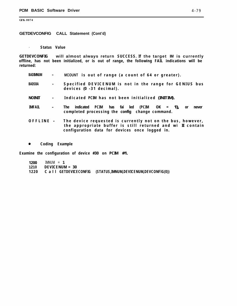
PCIM BASIC Software Driver 4 - 7 9
GFK-0074
GETDEVCONFIG CALL Statement (Cont’d)
- Status Value
GETDEVCONFIG will almost always return SUCCESS. If the target IM is currentlyoffline, has not been initialized, or is out of range, the following FAIL indications will bereturned:
BADIMNUM - MCOUNT i s o u t o f r a n g e ( a c o u n t o f 6 4 o r g r e a t e r ) .
BADSBA - S p e c i f i e d D E V I C E N U M i s n o t i n t h e r a n g e f o r G E N I U S b u sd e v i c e s (0 - 3 1 d e c i m a l ) .
NOINIT - I n d i c a t e d PCIM h a s n o t b e e n i n i t i a l i z e d (INITIM).
IMFAIL - The indicated PCIM has fai led (PCIM OK = 1), or neverc o m p l e t e d p r o c e s s i n g t h e config c h a n g e c o m m a n d .
O F F L I N E - T h e d e v i c e r e q u e s t e d i s c u r r e n t l y n o t o n t h e b u s , h o w e v e r ,t h e a p p r o p r i a t e b u f f e r i s s t i l l r e t u r n e d a n d w i II c o n t a i nc o n f i g u r a t i o n d a t a f o r d e v i c e s o n c e l o g g e d i n .
Coding Example
Examine the configuration of device #30 on PCIM #1.
1200 IMNUM = 11210 DEVICENUM = 301 2 2 0 C a l l GETDEVICECONFIG (STATUS,IMNUM,DEVICENUM,DEVCONFlG(0))
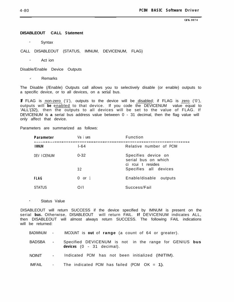
4-80 PCIM BASIC Software Dr iver
GFK-0074
DISABLEOUT CALL Statement
- Syntax
CALL DISABLEOUT (STATUS, IMNUM, DEVICENUM, FLAG)
- Act ion
Disable/Enable Device Outputs
? Remarks
The Disable (/Enable) Outputs call allows you to selectively disable (or enable) outputs toa specific device, or to all devices, on a serial bus.
If FLAG is non-zero (‘1'), outputs to the device will be disabled; if FLAG is zero ('0’),outputs will be enabled to that device. If you code the DEVICENUM value equal to'ALL’(32), then the outputs to all devices will be set to the value of FLAG. IfDEVICENUM is a serial bus address value between 0 - 31 decimal, then the flag value willonly affect that device.
Parameters are summarized as follows:
Parameter Va I ues Function-___----------------_________I__________----------------------------I MNUM l-64 Relative number of PCIM
DEV I CENUM 0-32
3 2
Specifies device onserial bus on whichci rcui t residesSpecifies all devices
F L A G 0 or 1 Enable/disable outputs
STATUS O / l Success/Fail
- Status Value
DISABLEOUT will return SUCCESS if the device specified by IMNUM is present on theserial bus. Otherwise, DISABLEOUT will return FAIL. If DEVICENUM indicates ALL,then DISABLEOUT will almost always return SUCCESS. The following FAIL indicationswill be returned:
BADIMNUM - IMCOUNT is out of range (a count of 64 or greater).
BADSBA - Specified DEVICENUM is not in the range for GENIUS busdevices (0 - 31 decimal).
NOINIT - Indicated PCIM has not been initialized (INITIM).
IMFAIL - The indicated PCIM has failed (PCIM OK = 1).

PCIM BASIC Software Driver 4 - 8 1
GFK-0074
DISABLEOUT CALL Statement (Cont’d)
a Coding Example
Enable outputs to device #8 on PClM #1.
1 6 0 0 DEVICENUM = 81 6 1 0 IMNUM = 11620 F L A G = 01 6 3 0 C a l l DISABLEOUT(STATUS,IMNUM,DEVICENUM,FLAG)
Disable outputs to all devices on PCIM #1.
1700 DEVICENUM = 321710 IMNUM = 11720 FLAG = 11730 C a l l DISABLEOUT(STATUS,IMNUM,DEVICENUM,FLAG)
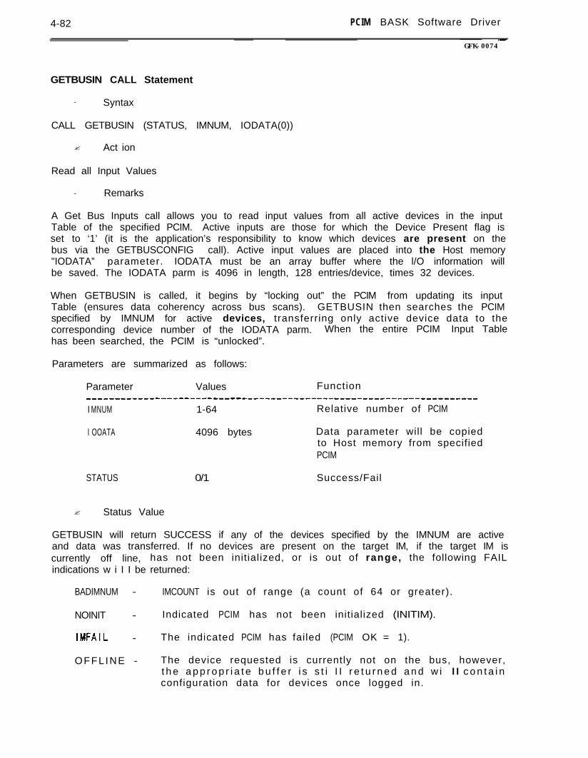
4-82 PCIM BASK Software Driver~-. ~~
GFK-0074
GETBUSIN CALL Statement
- Syntax
CALL GETBUSIN (STATUS, IMNUM, IODATA(0))
? Act ion
Read all Input Values
- Remarks
A Get Bus Inputs call allows you to read input values from all active devices in the inputTable of the specified PCIM. Active inputs are those for which the Device Present flag isset to ‘1’ (it is the application’s responsibility to know which devices are present on thebus via the GETBUSCONFIG call). Active input values are placed into the Host memory"IODATA” parameter. IODATA must be an array buffer where the l/O information willbe saved. The IODATA parm is 4096 in length, 128 entries/device, times 32 devices.
When GETBUSIN is called, it begins by “locking out” the PCIM from updating its inputTable (ensures data coherency across bus scans). GETBUSIN then searches the PCIMspecified by IMNUM for active devices, transferring only active device data to thecorresponding device number of the IODATA parm. When the entire PCIM Input Tablehas been searched, the PCIM is “unlocked”.
Parameters are summarized as follows:
Parameter Values Function-__-----------------------------------------------------------------I MNUM 1-64 Relative number of PCIM
I OOATA 4096 bytes Data parameter will be copiedto Host memory from specifiedPCIM
STATUS 0/1 Success/Fail
? Status Value
GETBUSIN will return SUCCESS if any of the devices specified by the IMNUM are activeand data was transferred. If no devices are present on the target IM, if the target IM iscurrently off line, has not been initialized, or is out of range, the following FAILindications w i I I be returned:
BADIMNUM - IMCOUNT is out of range (a count of 64 or greater).
NOINIT - Indicated PCIM has not been initialized (INITIM).
IMFAIL - The indicated PCIM has failed (PCIM OK = 1).
OFFL INE - The device requested is currently not on the bus, however,t h e a p p r o p r i a t e b u f f e r i s s t i I I r e t u r n e d a n d w i II c o n t a i nconfiguration data for devices once logged in.

PCIM BASIC Software Driver 4-03
GFK-0074
GETBUSIN CALL Statement (Cont’d)
- Coding Example
Read all inputs from all active devices on PCIM #1.
2000 IMNUM = 12010 C a l l GETBUSIN(STATUS,IMNUM,IODATA(O))

4-84 PCIM BASIC Software Driver
CFK-0074
PUTBUSOUT CALL Statement
? Syntax
CALL PUTBUSOUT (STATUS, IMNUM, lODATA(0))
- Act ion
Write all Output Values
- Remarks
The Put Bus Outputs call allows you to update outputs to ail active devices in the OutputTable of the specified PCIM. Active outputs are those with the Device Present flag setto ‘1’ (it is the application’s responsibility to know which devices are present on the busvia the GETBUSCONFIG call). Active output values are written from the Host memoryIODATA parameter. IODATA must be an array buffer where the I/O information issaved. The IODATA parm is 4096 in length, 128 entries/device, times 32 devices
When PUTBUSOUT is called, it begins by “locking-out” the PCIM from updating itsOutput Table (ensures data coherency across PCIM scans). PUTBUSOUT then searchesthe PCIM specified by IMNUM for active devices, transferring only to active devices datafrom the device number of the IODATA parm corresponding to the device’s slot in theOutput Table. When the entire PCIM Output Table has been searched, the PCIM is“un I ocked” .
Parameters are summarized as follows:
Parameter Values Function_____---_-----------____cc_I____________----------------------------I MNUM l-64 Relative number of PCIM
l O D A T A 4096 bytes Data parameter will be copiedfrom Host memory to specifiedPCIM (not to exceed 255parameter value).
STATUS 0/1 Success/Fai
- Status Value
PUTBUSOUT will return SUCCESS if any of the devices speci f ied by the IMNUM areactive and data was transferred. If no devices are present on the target IM, if the targetIM is currently offline, has not been initialized, or is out of range, the following FAILindications w i I t be returned:
BADIMNUM - IMCOUNT is out of range (a count of 64 or greater).
NOIN
I MFA
QFFL
I T - Indicated PCIM has not been initialized (INITIM).
L - The indicated PCIM has failed (PCIM OK = 1).
NE - Data was transferred to the specified buffer, however, nodevices were found on the bus.
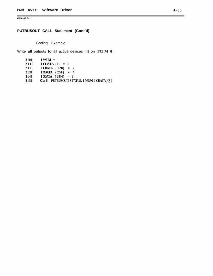
PCIM BASiC Software Driver 4-85
GFK-0074
PUTBUSOUT CALL Statement (Cont’d)
- Coding Example
Write all outputs to all active devices (4) on PCIM #l.
2100 IMNUM = 12110 IODATA (0) = 12120 IODATA (128) = 22130 IODATA (256) = 42140 IODATA (384) = 82150 C a l l PUTBUSOUT(STATUS,IMNUM,IODATA(O))

4-86 PCIM B A S I C S o f t w a r e D r i v e r
GFK-0074
GETDEVIN CALL Statement
- Syntax
CALL GETDEVIN (STATUS, IMNUM, DEVICENUM, LENGTH, DEVDATA(0))
? Act ion
Read Device Data Only
- Remarks
The GETDEVIN function allows you to read the control data inputs received from a singleserial bus device into the Host memory “DEVDATA” parameter.
IMNUM i s t h e PCIM n u m b e r c o n f i g u r e d d u r i n g i n i t i a l i z a t i o n . T h e DEVICENUMparameter specifies the serial bus address of the device from which input data is to beread. The “LENGTH parameter is the length of the input data the device sent. Thisway, the function can determine whether or not it should update its current data base.The “DEVDATA” parameter is a buffer data read will be located. The size of this bufferis determined by the “InputLength” parameter located in the device’s configuration data.
Parameters are summarized as follows:
Parameter Values Functionc----------------------------------------------------------------------------------------------------------------------------------------------------------------------------------------------------------------------------------------------------------------------------------------------------------------------------------------------------------------------------_- - - - - - - - - - - - - - - - - - - - - - - - - - - - -I MNUM l-64 R e l a t i v e n u m b e r o f PCIM
DEV I CENUM O-31 Specifies device onserial bus from whichinput data will be read
LENGTH O-128 Size of data buffer
DEVDATA v a r i a b l e Buffer where data in Hoststored - see above
STATUS 0/1 Success/Fail
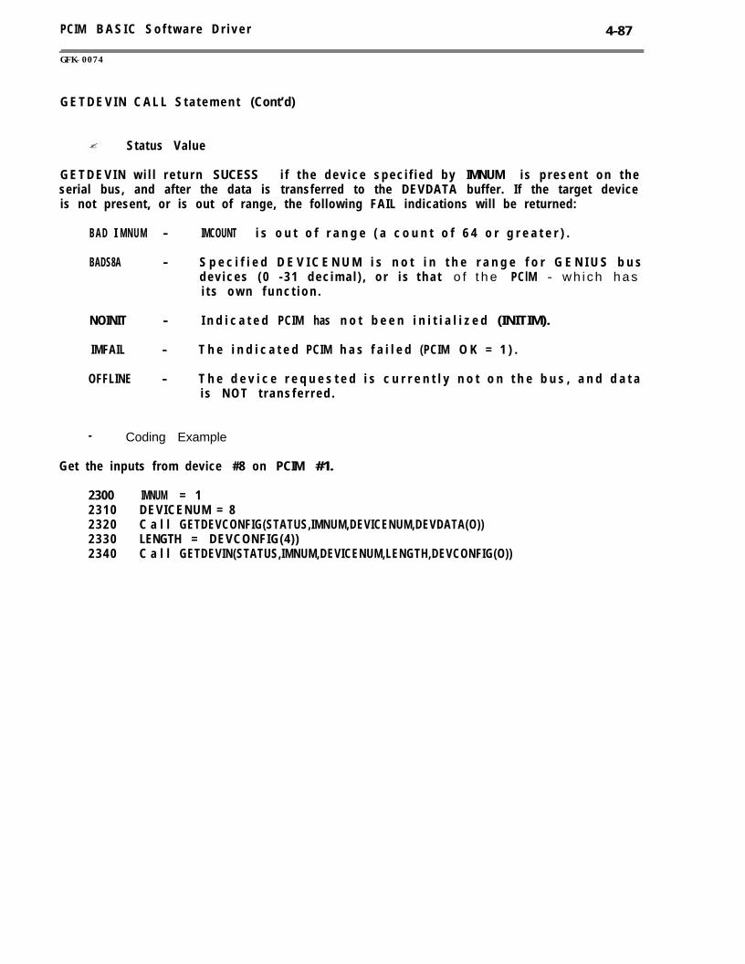
PCIM B A S I C S o f t w a r e D r i v e r 4-87
GFK-0074
G E T D E V I N C A L L S t a t e m e n t (Cont’d)
? Status Value
G E T D E V I N w i l l r e t u r n SUCESS i f t h e d e v i c e s p e c i f i e d b y IMNUM i s p r e s e n t o n t h eserial bus, and after the data is transferred to the DEVDATA buffer. If the target deviceis not present, or is out of range, the following FAIL indications will be returned:
BAD I MNUM - IMCOUNT i s o u t o f r a n g e ( a c o u n t o f 6 4 o r g r e a t e r ) .
BADS8A - S p e c i f i e d D E V I C E N U M i s n o t i n t h e r a n g e f o r G E N I U S b u sd e v i c e s ( 0 - 3 1 d e c i m a l ) , o r i s t h a t o f t h e PClM - w h i c h h a si t s o w n f u n c t i o n .
NOINIT - I n d i c a t e d PCIM has n o t b e e n i n i t i a l i z e d (INITIM).
IMFAIL - T h e i n d i c a t e d PCIM h a s f a i l e d (PCIM O K = 1 ) .
OFFLINE - T h e d e v i c e r e q u e s t e d i s c u r r e n t l y n o t o n t h e b u s , a n d d a t ai s N O T t r a n s f e r r e d .
- Coding Example
Get the inputs from device #8 on PCIM #1.
2300 IMNUM = 12 3 1 0 DEVICENUM = 82 3 2 0 C a l l GETDEVCONFIG(STATUS,IMNUM,DEVICENUM,DEVDATA(O))2 3 3 0 LENGTH = DEVCONFIG(4))2 3 4 0 C a l l GETDEVIN(STATUS,IMNUM,DEVICENUM,LENGTH,DEVCONFIG(O))
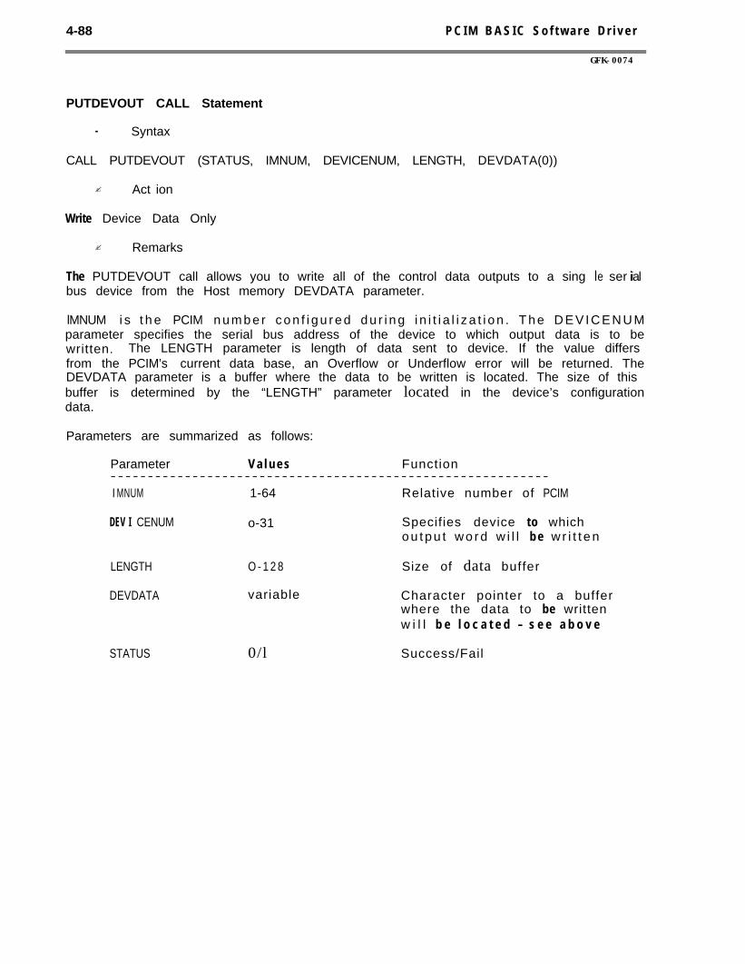
4-88 P C I M B A S I C S o f t w a r e D r i v e r
GFK-0074
PUTDEVOUT CALL Statement
- Syntax
CALL PUTDEVOUT (STATUS, IMNUM, DEVICENUM, LENGTH, DEVDATA(0))
? Act ion
Write Device Data Only
? Remarks
The PUTDEVOUT call allows you to write all of the control data outputs to a singbus device from the Host memory DEVDATA parameter.
le ser ial
lMNUM i s t h e PCIM n u m b e r c o n f i g u r e d d u r i n g i n i t i a l i z a t i o n . T h e D E V I C E N U Mparameter specifies the serial bus address of the device to which output data is to bewritten. The LENGTH parameter is length of data sent to device. If the value differsfrom the PCIM’s current data base, an Overflow or Underflow error will be returned. TheDEVDATA parameter is a buffer where the data to be written is located. The size of thisbuffer is determined by the “LENGTH” parameter located in the device’s configurationdata.
Parameters are summarized as follows:
Parameter V a l u e s Function- - - - - - - - - - - - - - - - - - - - - - - - - - - - - - - - - - - - - - - - - - - - - - - - - - - - - - - - - - -I MNUM 1-64 Relative number of PCIM
DEV I CENUM o-31 Specifies device to whicho u t p u t w o r d w i l l b e w r i t t e n
LENGTH O - 1 2 8 Size of data buffer
DEVDATA variable Character pointer to a bufferwhere the data to be writtenw i l l b e l o c a t e d - s e e a b o v e
STATUS 0/l Success/Fail
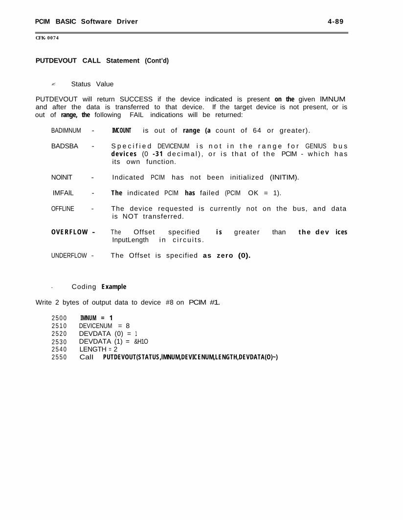
PCIM BASIC Software Driver 4-89
CFK-0074
PUTDEVOUT CALL Statement (Cont’d)
? Status Value
PUTDEVOUT will return SUCCESS if the device indicated is present on the given lMNUMand after the data is transferred to that device. If the target device is not present, or isout of range, the foIlowing FAIL indications will be returned:
BADIMNUM -
BADSBA -
NOlNlT -
IMFAlL -
OFFLINE -
OVERFLOW -
UNDERFLOW -
IMCOUNT is out of range (a count of 64 or greater).
S p e c i f i e d DEVICENUM i s n o t i n t h e r a n g e f o r GENlUS b u sd e v i c e s (0 - 3 1 d e c i m a l ) , o r i s t h a t o f t h e PCIM - w h i c h h a sits own function.
Indicated PCIM has not been initialized (INITIM).
The indicated PClM has failed (PCIM OK = 1).
The device requested is currently not on the bus, and datais NOT transferred.
The Offset specified i s greater than the dev icesInputLength i n c i r c u i t s .
The Offset is specified as zero (0).
- Coding Example
Write 2 bytes of output data to device #8 on PCIM #1.
2 5 0 0 IMNUM = 12 5 1 0 DEVICENUM = 82 5 2 0 DEVDATA (0) = 12 5 3 0 DEVDATA (1) = &H1O2 5 4 0 LENGTH = 22 5 5 0 CalI PUTDEVOUT(STATUS,lMNUM,DEVICENUM,LENGTH,DEVDATA(O)~)
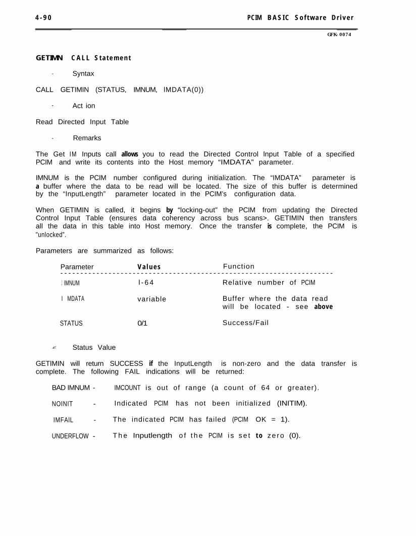
4 - 9 0 PCIM B A S I C S o f t w a r e D r i v e r
GFK-0074
GETIMN C A L L S t a t e m e n t
- Syntax
CALL GETIMIN (STATUS, IMNUM, lMDATA(0))
- Act ion
Read Directed Input Table
- Remarks
The Get IM Inputs call allows you to read the Directed Control lnput Table of a specifiedPCIM and write its contents into the Host memory “IMDATA” parameter.
IMNUM is the PCIM number configured during initialization. The “IMDATA” parameter isa buffer where the data to be read will be located. The size of this buffer is determinedby the “InputLength” parameter located in the PCIM’s configuration data.
When GETIMIN is called, it begins by “locking-out” the PCIM from updating the DirectedControl Input Table (ensures data coherency across bus scans>. GETIMIN then transfersall the data in this table into Host memory. Once the transfer is complete, the PCIM is"unlocked”.
Parameters are summarized as follows:
Parameter V a l u e s Function- - - - - - - - - - - - - - - - - - - - - - - - - - - - - - - - - - - - - - - - - - - - - - - - - - - - - - - - - - - - - - - - - - - -
J IMNUM l - 6 4 Relative number of PCIM
I MDATA variable Buffer where the data readwill be located - see above
STATUS 0/1 Success/Fail
? Status Value
GETIMIN will return SUCCESS if the InputLength is non-zero and the data transfer iscomplete. The following FAIL indications will be returned:
BAD IMNUM - IMCOUNT is out of range (a count of 64 or greater).
NOINIT - Indicated PCIM has not been initialized (INITIM).
IMFAlL - The indicated PCIM has failed (PCIM OK = 1).
UNDERFLOW - T h e Inputlength o f t h e PCIM i s s e t t o ze ro (0).
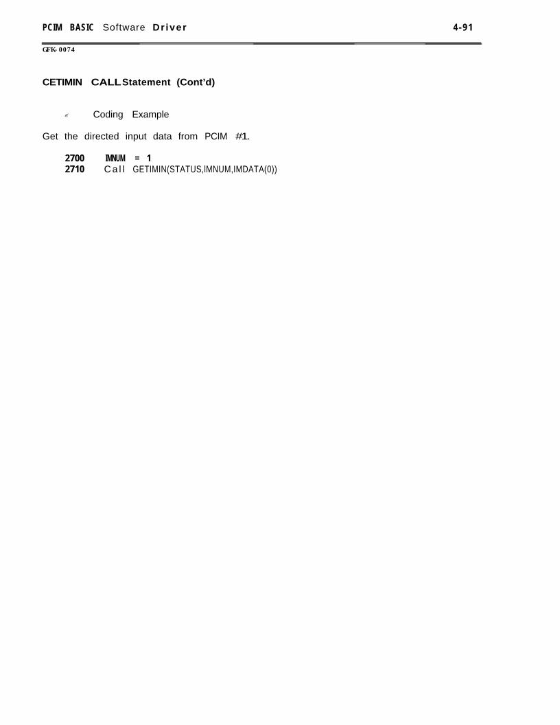
PCIM BASIC Software Dr iver 4 - 9 1
GFK-0074
CETIMIN CALL Statement (Cont’d)
? Coding Example
Get the directed input data from PCIM #1.
2700 IMNUM = 12710 C a l l GETIMIN(STATUS,lMNUM,IMDATA(0))

4-92 PCIM BASIC Software Driver
GFK-0074
PUTIMOUT CALL Statement
? Syntax
CALL PUTIMOUT (STATUS, IMNUM, IMDATA(O))
? Act ion
Write the Global Output Table
- Remarks
The Put IM Outputs call allows you to write Control Data from the Host memory IMdataparameter to the Broadcast Control Output Table of a specified PCIM. This data issubsequently passed to ail devices on that PCIM.
IMNUM is the PCIM number configured during initialization. The IMDATA parameter is abuffer where the data to be written is located. The size of this buffer is determined bythe “GlobalLength” parameter located in the device’s configuration data.
When PUTIMOUT is called, it begins by “locking-out” the PCIM from reading from itsControl Output Table (ensures data coherency across bus scans>. PUTIMOUT thentransfers all the data from this parm to the PCIM’s Global Output buffer. Once thetransfer is complete, the PCIM is “unlocked”.
Parameters are summarized as follows:
Parameter Values Function---------------------------------------------------------------I MNUM t-64 Relative number of PCIM
I MDATA variable Buffer where the data to bew r i t t e n w i l l b e l o c a t e d- see above
STATUS 0/1 Success/Fail
? Status Value
PUTIMOUT will return SUCCESS if the Globallength is non-zero and the transfer iscomplete. The following FAIL indications will be returned:
BADIMNUM - IMCOUNT is out of range (a count of 64 or greater).
NOINIT - Indicated PCIM has not been initialized (INITIM).
IMFAIL - The indicated PClM has failed (PCIM OK = 1).
UNDERFLOW - The GlobalLength parameter in IMPARMS is set to zero (0).

PCIM BASIC Software Driver 4 - 9 3
GFK-0074
PUTIMOUT CALL Statement (Cont’d)
? Coding Example
Write the specified global data to PCIM #1.
2 8 0 0 IMNUM = 12 8 1 0 IMDATA (0) = &H102 8 2 0 C a l l PUTIMOUT(STATUS,IMNUM,iMDATA(0))
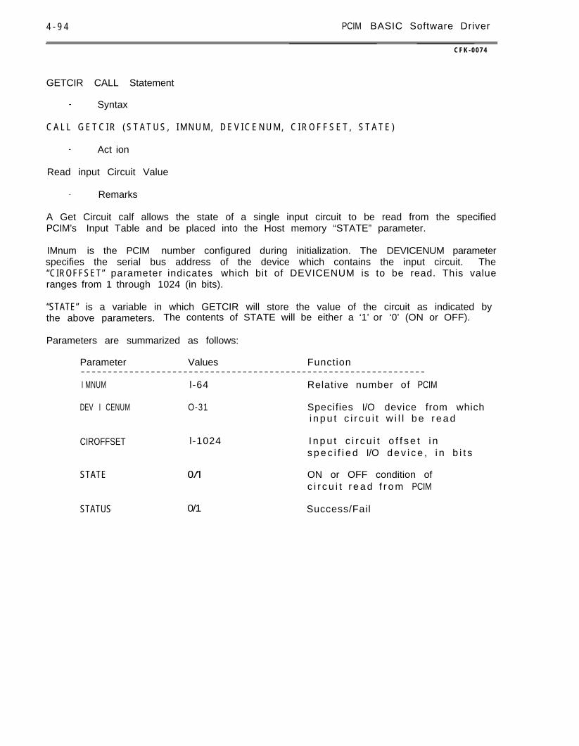
4 - 9 4 PCIM BASIC Software Driver
C F K - 0 0 7 4
GETCIR CALL Statement
- Syntax
C A L L G E T C I R ( S T A T U S , I M N U M , D E V I C E N U M , C I R O F F S E T , S T A T E )
- Act ion
Read input Circuit Value
- Remarks
A Get Circuit calf allows the state of a single input circuit to be read from the specifiedPCIM’s Input Table and be placed into the Host memory “STATE” parameter.
IMnum is the PCIM number configured during initialization. The DEVICENUM parameterspecifies the serial bus address of the device which contains the input circuit. The“CIROFFSET” parameter indicates which bit of DEVICENUM is to be read. This valueranges from 1 through 1024 (in bits).
“STATE” is a variable in which GETCIR will store the value of the circuit as indicated bythe above parameters. The contents of STATE will be either a ‘1’ or ‘0’ (ON or OFF).
Parameters are summarized as follows:
Parameter Values Function----------------------------------------------------------------I MNUM l-64 Relative number of PCIM
DEV I CENUM O-31 Specifies I/O device from whichi n p u t c i r c u i t w i l l b e r e a d
CIROFFSET l-1024 I n p u t c i r c u i t o f f s e t i ns p e c i f i e d I/O d e v i c e , i n b i t s
STATE 0/1 ON or OFF condition ofc i r c u i t r e a d f r o m PCIM
STATUS 0/1 Success/Fail

PCIM BASIC Software Driver 4-95
CFK-0074
GETCIR CALL Statement (Cont’d)
- Status Value
GETCIR will return SUCCESS if the target device is present on the given IMNUM. If thetarget device is not present, or is out of range, GETCIR will return FAIL. If SUCCESS isreturned, then STATE will contain the value of the circuit requested. The following FAILindications w i I I be returned:
BADIMNUM - IMCOUNT is out of range (a count of 64 or greater).
BADSBA - Specified DEVICENUM is not in the range for GENIUS busdevices (0 -31 decimal), or is that of the PCIM - which hasits own function.
NOINIT - Indicated PCIM has not been initialized (INITIM).
IMFAIL - The indicated PCIM has failed (PCIM OK = 1).
OFFL INE - The device requested is currently not on the bus, and datais NOT transferred.
OVERFLOW - T h e OFFSET specified is greater than t h e d e v i c e sInputLength i n c i r c u i t s .
UNDERFLOW - OFFSET is specified as zero (0).
0 Coding Example
Get the stat value of circuit 2 of device #8 on PCIM #1.
3000 IMNUM = 13 0 1 0 DEVICENUM = 83 0 2 0 CIROFFSET = 23 0 3 0 C a l l GETCIR(IMNUM,DEVICENUM,CIROFFSET,STATE)
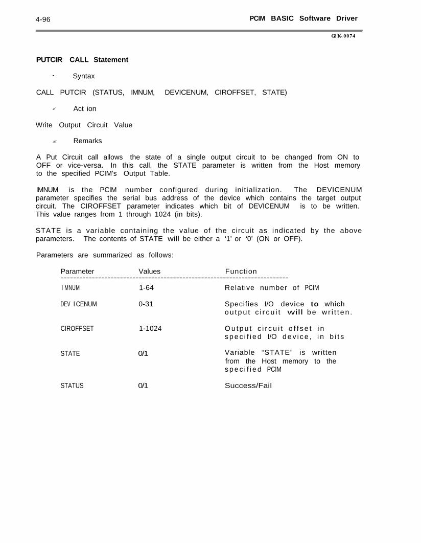
4-96 PCIM BASIC Software Driver
GfK-0074
PUTCIR CALL Statement
- Syntax
CALL PUTCIR (STATUS, IMNUM, DEVICENUM, CIROFFSET, STATE)
? Act ion
Write Output Circuit Value
? Remarks
A Put Circuit call allows the state of a single output circuit to be changed from ON toOFF or vice-versa. In this call, the STATE parameter is written from the Host memoryto the specified PCIM’s Output Table.
IMNUM is the PClM number configured during initialization. The DEVICENUMparameter specifies the serial bus address of the device which contains the target outputcircuit. The CIROFFSET parameter indicates which bit of DEVICENUM is to be written.This value ranges from 1 through 1024 (in bits).
STATE is a variable containing the value of the circuit as indicated by the aboveparameters. The contents of STATE will be either a ‘1’ or ‘0’ (ON or OFF).
Parameters are summarized as follows:
Parameter Values Function-------------------------------------------------------------------------I MNUM 1-64 Relative number of PCIM
DEV I CENUM 0-31 Specifies I/O device to whicho u t p u t c i r c u i t will b e w r i t t e n .
CIROFFSET 1-1024 O u t p u t c i r c u i t o f f s e t i ns p e c i f i e d I/O d e v i c e , i n b i t s
STATE 0/1 Variable “STATE” is writtenfrom the Host memory to thes p e c i f i e d PCIM
STATUS 0/1 Success/FaiI
PCIM BASIC Software Driver 4-97
GFK-0074
PUTCIR CALL Statement (Cont’d)
- Status Value
PUTClR will return SUCCESS if the target device is present on the given IMNUM. If thetarget device is not present, or is out of range, PUTClR will return FAIL. I f SUCCESS isreturned, then the character pointed to by STATE will contain the value of the circuitchanged. The following FAIL indications will be returned:
B A D lMNUM - IMCOUNT i s o u t o f r a n g e ( a c o u n t o f 6 4 o r g r e a t e r ) .
BADSBA - S p e c i f i e d DEVICENUM i s n o t i n t h e r a n g e f o r G E N I U S b u sd e v i c e s (0 -31 d e c i m a l ) , o r i s t h a t o f t h e PCIM - w h i c h h a si t s o w n f u n c t i o n .
NOINIT - I n d i c a t e d PCIM h a s n o t b e e n i n i t i a l i z e d (INITIM).
IMFAIL - T h e i n d i c a t e d PCIM h a s f a i l e d (PCIM O K = 1 ) .
O F F L I N E - T h e d e v i c e r e q u e s t e d i s c u r r e n t l y n o t o n t h e b u s , a n d d a t ai s N O T t r a n s f e r r e d .
OVERFLOW - The O F F S E T s p e c i f i e d is g r e a t e r than the dev icesOutputLength i n c i r c u i t s .
UNDERFLOW - O F F S E T i s s p e c i f i e d a s z e r o (0).
? Coding Example
Set the state value of circuit 2 of device #8 on PCIM #1 to ‘1 I.
3200 IMNUM = 13 2 1 0 DEVl CENUM = 83 2 2 0 STATE = 13 2 3 0 CIROFFSET = 23 2 4 0 C a l l PUTCIR(STATUS,IMNUM,DEVICENUM,CIROFFSET,STATE)
4-98 PCIM B A S I C S o f t w a r e D r i v e r
GFK-0074
GETWORD CALL Statement
- Syntax
CALL GETWORD (STATUS, IMNUM, DEVICENUM, CIROFFSET, WORDDATA)
- Act ion
Read Input Word Value
- Remarks
A Get Word call allows you to read the value of a single input word from the specifiedPCIM’s Input Table into the Host memory “WORDDATA” parameter. The “WORDDATATAparameter is an integer.
IMNUM i s t h e PCIM n u m b e r c o n f i g u r e d d u r i n g i n i t i a l i z a t i o n . T h e D E V I C E N U Mparameter specifies the serial bus address of the device where the input word is located.The CIROFFSET parameter indicates which word of the specified device is to be read.This value ranges from 1 through 64 (in word quantities).
When GETWORD is called, it begins by "locking-out” the PCIM from updating the SharedRAM (ensures data coherency across bus scans>. GETWORD then transfers the word datainto Host memory. Once the transfer is complete, the PCIM is ‘unlocked”.
Parameters are summarized as follows:
Parameter Values Function-----------------------------------------------------------------I MNUM 1-64 Relative number of PCIM
DEV I CENUM o-31 Specifies I/O device from whichinput word wi I I be read
CIROFFSET 1-64 Input word offset inspecified I/O device, in words
WORDDATA 1 entry Word requested
STATUS 0/1 Success/Fail
PCIM BASIC Software Driver 4-99
GFK-0074
GETWORD CALL Statement (Cont’d)
- Status Value
GETWORD w i l l r e t u r n S U C C E S S i f t h e d e v i c e s p e c i f i e d b y IMNUM i s p r e s e n t o n t h es e r i a l b u s , a n d a f t e r t h e d a t a i s t r a n s f e r r e d t o W O R D D A T A . I f t h e t a r g e t d e v i c e i s n o tp r e s e n t , o r i s o u t o f r a n g e , GETWORD w i l l r e t u r n F A I L . I f S U C C E S S i s r e t u r n e d , t h e nthe requested word value will be saved in the location WORDDATA. The following FAILindications w i I I be returned:
BADIMNUM - IMCOUNT i s o u t o f r a n g e ( a c o u n t o f 6 4 o r g r e a t e r ) .
BADSBA - S p e c i f i e d D E V I C E N U M i s n o t i n t h e r a n g e f o r G E N I U S b u sd e v i c e s ( 0 - 3 1 d e c i m a l ) , o r i s t h a t o f t h e PCIM - w h i c h h a si t s o w n f u n c t i o n .
NOINIT - I n d i c a t e d PCIM h a s n o t b e e n i n i t i a l i z e d (INITIM).
IMFAlL - T h e i n d i c a t e d PCIM h a s f a i l e d (PCIM O K = 1 ) .
O F F L I N E - T h e d e v i c e r e q u e s t e d i s c u r r e n t l y n o t o n t h e b u s , a n d d a t ai s N O T t r a n s f e r r e d .
OVERFLOW - T h e O F F S E T speci f ied i s g r e a t e r t h a n the d e v i c e sInputLength i n c i r c u i t s .
UNDERFLOW - O F F S E T i s s p e c i f i e d a s z e r o ( 0 ) .
? Coding Example
Get the first word of device #8 on PCIM #1.
3 3 0 0 IMNUM = 13 3 1 0 DEVICENUM = 83 3 2 0 CIROFFSET = 13 3 3 0 C a l l GETWORD(STATUS,IMNUM,DEVICENUM,ClROFFSET,WORDDATA)

4-l 00 PCIM BASIC Software Driver
GFK-0074
PUTWORD CALL Statement
? Syntax
CALL PUTWORD (STATUS, IMNUM, DEVICENUM, ClROFFSET, WORDDATA)
? Act ion
Write Output Word Value
- Remarks
A Put Word call allows you to write a single output word from the Host memoryWORDDATA parameter t o t h e s p e c i f i e d PCIM’s O u t p u t Table. T h e WORDDATAparameter is an integer which PUTWORD uses to store the word to be transmitted.
lMNUM i s t h e PCIM n u m b e r c o n f i g u r e d d u r i n g i n i t i a l i z a t i o n . T h e DEVlCENUMparameter specifies the serial bus address of the device where the output word is to besent. The ClROFFSET parameter indicates which word of the specified device is to bewritten. This value ranges from 1 through 64 (in word quantities).
When PUTWORD is called, it begins by “locking-out” the PClM from updating the SharedRAM (ensures data coherency across bus scans). PUTWORD then transfers the word datato the PCIM. Once the transfer is complete, the PClM is “unlocked”.
Parameters are summarized as follows:
Parameter Values Function- - - - - - - - - - - - - - - - - - - - - - - - - - - - - - - - - - - - - - - - - - - - - - - - - - - - - - - -I MNUM 1-64 Relative number of PClM
DEVICENUM 0-31 Specifies device to whichoutput word will be written
CI ROFFSET 1 - 6 4 Output word offset in specifieddevice, in words
WORDDATA 1 entry Word requested
STATUS 0/1 Success/FaiI

PCIM B A S I C S o f t w a r e D r i v e r 4-101
GFK-0074
PUTWORD CALL Statement (Cont’d)
- Status Value
PUTWORD w i l l r e t u r n S U C C E S S i f t h e d e v i c e s p e c i f i e d b y IMNUM i s p r e s e n t o n t h eserial bus. If the target device is not present, or is out of range, PUTWORD will returnFAIL. The following FAIL indications will be returned:
BADIMNUM - IMCOUNT i s o u t o f r a n g e ( a c o u n t o f 6 4 o r g r e a t e r ) .
BADSBA - S p e c i f i e d D E V I C E N U M i s n o t i n t h e r a n g e f o r G E N I U S b u sd e v i c e s (0 - 3 1 d e c i m a l ) , o r i s t h a t o f t h e PCIM - w h i c h h a si t s o w n f u n c t i o n .
NOINIT - I n d i c a t e d PCIM h a s n o t b e e n i n i t i a l i z e d (INlTlM).
IMFAIL - T h e i n d i c a t e d PCIM h a s f a i l e d (PCIM O K = 1 ) .
O F F L I N E - T h e d e v i c e r e q u e s t e d i s c u r r e n t l y n o t o n the b u s , a n d d a t ai s N O T t r a n s f e r r e d .
OVERFLOW - T h e O F F S E T s p e c i f i e d i s g r e a t e r than t h e d e v i c e sOutputLength i n c i r c u i t s .
UNDERFLOW - O F F S E T i s s p e c i f i e d a s z e r o (0).
- Coding Example
Set the second word of device #8 on PCIM #1 to 10 hex (circuit #21 if discrete block).
3 4 0 0 IMNUM = 13 4 1 0 DEVICENUM = 83 4 2 0 CIROFFSET = 23 4 3 0 WORDDATA = &H103 4 4 0 C a l l PUTWORD(STATUS,IMNUM,DEVICENUM,CIROFFSET,WORDDATA)
4-l 02 PCIM BASIC Software Driver
GFK-0074
SENDMSG CALL Statement
? Syntax
CALL SENDMSG (STATUS, IMNUM, MSG(0))
- Act ion
Send a Message
? Remarks
The Send Message call allows you to write a memory or non-memory message from theHost to the selected PCIM for transmission onto the serial bus (using the TransmitDatagram command). SENDMSG will return control to the calling program without delay,before the message has been processed or transmitted by the PCIM.
IMNUM defines the PCIM, as configured during initialization, from which to transmit themessage. The MSG parameter is the buffer where the transmit message is stored.
The format of SENDMSG is:
MSGCO) Destination (0-31/255 brdcst) - Destination address of DeviceMSG(1) Function code (O-111) - Function CodeMSG(2) SubFunction code (O-255) - Sub Function CodeMSG(3) P r i o r i t y -0- Normal, 1 - HighMSGW(4) Length - Data field length/length of msgMSG(5) Data (variable) - Message Data - length per MSG(4)
You can check the status of the message using CHKMSGSTAT to determine if themessage completed processing properly.
Parameters are summarized as follows:
Parameter Values Function______-----------------------_______________----------------------------IIMNUM 1-64 Relative number of PCIM
M S G see above Buffer where messageto be sent is stored- see above
STATUS 0/1 Success/Fail
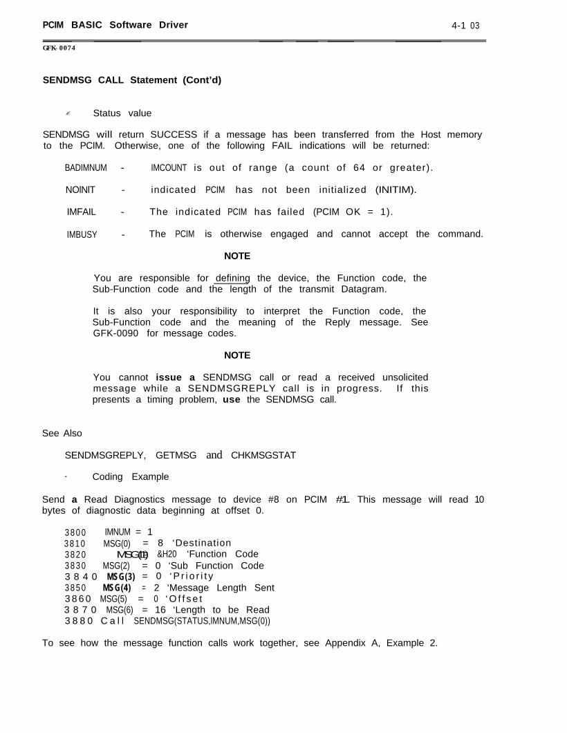
PCIM BASIC Software Driver 4-1 03
GFK-0074
SENDMSG CALL Statement (Cont’d)
? Status value
SENDMSG will return SUCCESS if a message has been transferred from the Host memoryto the PCIM. Otherwise, one of the following FAIL indications will be returned:
BADIMNUM - IMCOUNT is out of range (a count of 64 or greater).
NOlNlT - indicated PCIM has not been initialized (INITIM).
IMFAIL - The indicated PCIM has failed (PCIM OK = 1).
IMBUSY - The PCIM is otherwise engaged and cannot accept the command.
NOTE
You are responsible for defining the device, the Function code, theSub-Function code and the length of the transmit Datagram.
It is also your responsibility to interpret the Function code, theSub-Function code and the meaning of the Reply message. SeeGFK-0090 for message codes.
NOTE
You cannot issue a SENDMSG call or read a received unsolicitedmessage while a SENDMSGREPLY call is in progress. If thispresents a timing problem, use the SENDMSG call.
See Also
SENDMSGREPLY, GETMSG and CHKMSGSTAT
- Coding Example
Send a Read Diagnostics message to device #8 on PCIM #1. This message will read 10bytes of diagnostic data beginning at offset 0.
3 8 0 0 IMNUM = 13 8 1 0 MSG(0) = 8 ‘Destination3 8 2 0 MSG(I1)= &H20 ‘Function Code3 8 3 0 MSG(2) = 0 ‘Sub Function Code3 8 4 0 MSG(3) = 0 ‘ P r i o r i t y3 8 5 0 MSG(4) = 2 ‘Message Length Sent3 8 6 0 MSG(5) = 0 ‘ O f f s e t3 8 7 0 MSG(6) = 16 ‘Length to be Read3 8 8 0 C a l l SENDMSG(STATUS,lMNUM,MSG(0))
To see how the message function calls work together, see Appendix A, Example 2.
4-104 PCIM BASIC Software Dr iver
G F K - 0 0 7 4
SENDMSGREPLY CALL Statement
- Syntax
CALL SENDMSGREPLY (STATUS, IMNUM, MSG(0))
- Act ion
Send a Message requesting a Reply
- Remarks
The Send Message Reply call allows you to write a memory or non-memory message fromthe Host to the selected PCIM for transmission onto the bus (using the TransmitDatagram With Reply command). SENDMSGREPLY will return control to the callingprogram without waiting for the reply. You must call CHKMSGSTAT or GETMSG tocheck for completion or to read the reply message.
IMNUM defines the PCIM, as configured during initialization, from which to transmit themessage. The MSG parameter is a pointer to the buffer where the transmit message isstored.
The format of SENDMSGREPLY is:
MSG(O) D e s t i n a t i o n (0-31/255 brdcst) - Destination address of DeviceMSG(1) Function code (0-111) - Function CodeMSG(2) T SubFunction code (0-255) - Transmted Reply SubFunction CodeMSG(3) R SubFunction code (0-255)MSG(4) P r i o r i t y
- Expected Reply SubFunction Code- 0 - Normal, 1 - High
MSG(5) Length (0-134) - Data field length/length of msgMSG(6) Data (variable) - Message Data - length per MSG(5)
You can check the status of the message using CHKMSGSTAT to determine if themessage completed processing properly.
Parameters are summarized as follows:
Parameter Values Function---------------------------------------------------------------------------------------------------------------I MNUM 1-64 Relative number of PCIM
MSG see above Pointer to the buffer wherethe received message will bestored - see above
STATUS 0/1 Success/Fail
PCIM BASIC Software Driver 4-105
GFK-0074
SENDMSGREPLY CALL Statement (Cont’d)
The advantage of the SENDMSGREPLY call over the SENDMSG call is twofold:
1) Allows a Read ID message to be sent (cannot be sent using the SENDMSG call).
2) Reduces user programming since a 10 second timeout to a non-responding deviceis automatically provided by the PCIM for a SENDMSGREPLY calf.
The Host program sequence for a SENDMSGREPLY is as follows:
1) Host sends a SENDMSGREPLY to the PCIM.
2) Host issues GETMSG calls until the Status indicates completion. GETMSG willalso return the reply message into Host memory.
- Status Value
SENDMSGREPLY will return SUCCESS if a message has been transferred from the Hostmemory to the PCIM. Otherwise, one of the following FAIL indications will be returned:
BADIMNUM - IMCOUNT is out of range (a count of 64 or greater).
NOINIT - Indicated PCIM has not been initialized (INITIM).
IMFAIL - The indicated PCIM has failed (PCIM OK = 1).
IMBUSY - The PCIM is otherwise engaged and cannot accept the command.
NOTE
You are responsible for defining the device, the Function code, theSub-Function code and the length of the transmit Datagram.
It is also your responsibility to interpret the Function code, theSub-Function code and the meaning of the Reply message. SeeGFK-0090 for message codes.
NOTE
You cannot issue a SENDMSG call or read a received unsolicitedmessage while a SENDMSGREPLY call is in progress. If thispresents a timing problem, use the SENDMSG call.

4-106 PCIM BASIC Software Driver
GFK-0074
SENDMSGREPLY CALL Statement (Cont’d)
See Also
SENDMSG, GETMSG and CHKMSGSTAT
- Coding Example
This example sends a Read Diagnostics message to device #8 on PCIM #1 and expects areply message of Read Diagnostics Reply. This message requests 10 bytes of diagnosticdata beginning at offset 10.
4 0 0 0 IMNUM = 14 0 1 0 MSG(0) = 8 ‘Destination4 0 2 0 MSG(1) = &H20 ‘Function Code4 0 3 0 MSG(2) = 8 ‘Transmit SubFunction Code4 0 4 0 MSG(3) = 9 ‘Excepted Repty SubFunction Code4 0 5 0 MSG(4) = 0 ‘ P r i o r i t y4 0 6 0 MSGW(5) = 2 ‘Message Length Transmitted4 0 7 0 MSG(6) = 16 ‘Offset4 0 8 0 MSG(7) = 16 ‘Message Length to be Read4 0 9 0 C a l l SENDMSGREPLY(STATUS,IMNUM,MSG(0))
To see how the message function calls work together, see Appendix A, Example 2.
PCIM BASIC Software Driver 4-l 07
GFK-0074
CHKMSGSTAT CALL Statement
- Syntax
CALL CHKMSGSTAT (STATUS, IMNUM, MSGSTATUS(0))
- Act ion
Read Message Progress Status
- Remarks
The Check Message Status call allows you to determine the status of a previousSENDMSG call - that is, to determine when a transmitted message has actually beenreceived, and its completion status.
IMNUM i s t h e PCIM n u m b e r c o n f i g u r e d d u r i n g i n i t i a l i z a t i o n . T h e “MSGSTATUS”parameter is the returned message status.
The “MSGSTATUS” parameter will contain the following values:
I MFREEI MBUSYSUCCESSBADPARMTXERR
There is currently no activity.Message is sti l l in progress.Message has successfully completed.Message contained a syntax error.Message cannot be transmitted.
Parameters are summarized as follows:
Parameter Values Function--------------------- - - - - - - - - - - - - - - - - - - - - - - - - - - - - - - - - - - -I MNUM l-64 Relative number of PCIM
MSGSTATUS 0/1 Returned message status
STATUS 0/1 Success/Fail
- Status Value
CHKMSGSTAT will normally return the Status requested and a SUCCESS indication.Otherwise, one of the following FAIL indications will be returned:
BADIMNUM - IMCOUNT is out of range (a count of 64 or greater).
NOINIT - Indicated PCIM has not been initialized (INITIM).
IMFAIL - The indicated PCIM has failed (PCIM OK = 1).
PCIMERR - There may be a problem with the PCIM firmware.
4-l 08 PCIM BASIC Software Driver
GFK-0074
CHKMSGSTAT CALL Statement (Cont’d)
See Also
SENDMSGREPLY, SENDMSG and GETMSG
- Coding Example
Check the message status area of PCIM #1.
4 2 0 0 IMNUM = 14210 C a l l CHKMSGSTATUS(STATUS,IMNUM,MSGSTATUS)
To see how the message function calls work together, see Appendix A, Example 2.
PCIM BASIC Software Driver 4-l 09
GFK-0074
GETMSG CALL Statement
? Syntax
CALL GETMSG (STATUS, IMNUM, MSG(O))
- Act ion
Read Received Message
? Remarks
The Get Message call allows you to read a received memory or non-memory message (ora reply to a previous SENDMSGREPLY call) from the selected PCIM into the Hostmemory “MSG” parameter.
IMNUM is the PCIM number configured during initialization. The “MSG” parameter is thebuffer where the received message will be stored.
The format of GETMSG is:
MSG (0) Source (0-31/255 brdcst) - Source address of DeviceMSG (1) Function code (0-111) - Function CodeMSG (2) SubFunction code (0-255) - Sub Function CodeMSG (3) DB_Indicator - D i r e c t e d (1)/Broadcast (0)MSG (4) Length (0-134) - Data field length/length of messageMSG (5) Data (variable) - Message Data - length per MSG(4)
Parameters are summarized as follows:
Parameter Values Function- - - - - - - - - - - - - - - - - - - - - - - - - - - - - - - - - - - - - - - - - - - - - - - - - - - - - - - - - - - - - - - - - - - -I MNUM f-64 Relative number of PCIM
STATUS 0/1 Success/Fail
M S G see above Buffer where thereceived message willbe stored - see above
GETMSG performs the following sequence:
1) If there is a previous call to SENDMSGREPLY, GETMSG checks to see if thetransmission has successfully completed, and transfers the response back to you.If the response completed with an error, or if in progress, GETMSG will return aFAIL indication.
2) If there is no previous call to SENDMSGREPLY, GETMSG checks to see if thereis a memory message, and transfers that message back to you.
4-110 PCIM BASIC Software Driver
GFK-0074
GETMSG CALL Statement (Cont’d)
3) If no memory messages exist, then GETMSG checks to see if there is anon-memory message, and transfers that message back to you.
4) If no messages are present, GETMSG returns with a FAIL status.
NOTE
Unsolicited memory or non-memory Datagrams received by thePCIM may not be read by the Host while a SENDMSGREPLY is inprogress. This significantly affects Host response time to servicereceived Datagrams. If this is a problem, use the SENDMSG callinstead of SENDMSGREPLY.
a Status Value
GETMSG will return SUCCESS if a memory or non-memory message is returned to you.Otherwise, one of the following FAIL indications will be returned:
BADIMNUM - IMCOUNT is out of range (a count of 64 or greater).
NOlNlT - Indicated PCIM has not been initialized (INlTlM).
lMFAlL - The indicated PCIM has failed (PCIM OK = 1).
IMBUSY - The PCIM is otherwise engaged and cannot accept the command.
NOMSG - No message is available to be received at this time.
TXERR - A message transmission has failed.
PCIMERR - There may be a problem with the PCIM firmware.
See Also
SENDMSGREPLY, SENDMSG and CHKMSGSTAT
PCIM BASIC Software Driver 4-111
GETINTR CALL Statement
? Syntax
CALL GETINTR (STATUS, IMNUM, lNTR(0))
a Act ion
Read Interrupt Status Table
- Remarks
The Get Interrupt call allows you to read the selected PCIM’s Interrupt Status Table.You can read this table to:
see why an interrupt in the Host system has occurred
report the event in a non-interrupt environment, as is the default state of theSoftware Driver concept (the PCIM will still report the event even though theinterrupt is disabled).
Thus, the Interrupt Status Table can be polled (by reading and interpreting it) todetermine what is interrupting the PCIM. Interrupt conditions are discussed in chapter 2of this manual.
When GETINTR is called, it transfers the data from the PCIM’s Interrupt Status Table tothe Host memory “INTR” parameter. The format of the Interrupt Status Table is shownbelow.
IMNUM defines the PCIM, as configured during initiafization, from which the InterruptStatus Table is to be read. The lNTR parameter is the buffer where the Interrupt StatusTable information is stored. The values in the table below are: 0 = No interrupt occurred,1 = Interrupt occurred.
Position Explanation
The format of the INTR table is:
INTR(0)INTR(1)INTR(2)INTR(3)INTR(4)INTR(5)INTR(6)
- Summary if interrupt occurred.- Received memory datagram.- PCIM Status Change - usually fatal.- Device Status Change.- Outputs sent - end of bus access.- Command Block completed.- Received Datagram.
4-112 PCIM BASIC Software Driver
GETINTR CALL Statement (Cont’d)
After data transfer to the Host is complete, GETINTR clears all of the PCIM’s InterruptStatus Table bytes each time it is called. This way, you can see the latest event that hasoccurred each call.
Parameters are summarized as follows:
Parameter Values Function-------------------------- - - - - - - - - - - - - - - - - - - - - - - - - - - -I MNUM 1-64 Relative number of PCIM
I NTR see above Buffer where the table datawi Il l be stored
- Status Value
GETINTR will return SUCCESS if the device specified by IMNUM is present on the serialbus. If the target device is not present, or is out of range, GETINTR will return FAIL.The following FAIL indications will be returned:
BADIMNUM - IMCOUNT is out of range (a count of 64 or greater).
NOINIT - Indicated PClM has not been initialized (INITIM).
IMFAIL - The indicated PCIM has failed (PCIM OK = 1).
- Coding Example
This example shows how, if an interrupt occurs on PCIM #1, to transfer the contents ofthat PCIM’s status table. Interpretation of bits will depend on which interrupt is enabled,and which application is to be run.
4 3 0 0 f IMNUM = 14 3 1 0 C a l l GETlNTR(STATUS,lMNUM,INTR(0))4 3 2 0 ‘Do what is necessary for interrupt processing

PCIM BASIC Software Driver 4-113
GFK-00 74
PUTINTR CALL Statement
- Syntax
CALL PUTINTR (STATUS, IMNUM, DISABLEINTR(0))
- Act ion
Write to the Interrupt Disable Table
? Remarks
The Put Interrupt call allows you to write to the selected PClM’s Interrupt DisableTable. The PUTlNTR call first initializes a table to Enable and Disable individualinterrupts as you require. The PUTINTR call then writes this table to the InterruptDisable Table on the PCIM. You can Enable or Disable interrupts in any mix; that is, on asingle call, some interrupts may be Enabled and some Disabled, all may be Enabled, or allof the interrupts may be Disabled. Interrupt conditions are discussed in chapter 2 of thismanua I.
When PUTlNTR is called, it transfers the data from the Host memory “DISABLEINTR”parameter to the PCIM’s Interrupt Disable Table. The format of the Interrupt DisableTable is shown below.
IMNUM defines the PCIM, as configured during initialization, to which DISABLEINTR willbe read. The DlSABLEINTR parameter is the buffer where the Interrupt Disable Tableinformation is stored. The values in the table below are: 0 = Enable, 1 = Disable.
The format of the DISABLEINTR table is:
Position Explanation
DISABL NTR(0) - Summary if interrupt occurred.D tI SABL NTR(1) - Received memory datagram,D I SABL NTR(2) - PCIM Status Change - usually fatal.D I SABL NTR(3) - D e v i c e S t a t u s C h a n g e .DISABL NTR(4) - O u t p u t s s e n t - end of bus access.D I SABL NTR(5) - Command Block completed.D I SABL lNTR(6) - Received Datagram.
4-114 PCIM BASIC Software Driver
GFK-0074
PUTINTR CALL Statement (Cont’d)
Parameters are summarized as follows:
Parameter Values Funct ion- - - - - - - - - - - - - - - - - - - - - - - - - - - - - - - - - - - - - - - - - - - - - - - - - - - - -I MNUM l - 6 4 Relative number of PCIM
DISABLEINTR see above Buffer from which enable/disabledata is sent
? Status Value
PUTINTR will return SUCCESS if the device specified by IMNUM is present on the serialbus. If the target device is not present, or is out of range, PUTINTR will return FAIL.The following FAIL indications will be returned:
BADIMNUM - IMCOUNT is out of range (a count of 64 or greater).
NOINIT - Indicated PCIM has not been initialized (INITIM).
IMFAlL - The indicated PCIM has failed (PCIM OK = 1).
- Coding Example
This example enables the Receive Datagram Interrupt.
7000 IMNUM = 17 0 1 0 For I = 0 to 67 0 2 0 DISABLEINTR(I) = 07 0 3 0 NEXT I7 0 4 0 DISABLEINTR(6) = 17 0 5 0 C a l l PUTINTR(STATUS,IMNUM,DISABLEINTR(0))
Communications 5 - 1
G F K - 0 0 7 4
CHAPTER 5COMMUNICATIONS
INTRODUCTION
PCIM applications may be considered on two levels; ‘basic’ operation, consisting of thatwhich is necessary to set up the PCIM and use it as a simple l/O controller; and‘advanced’ operation. Advanced operation details the use of expanded diagnostics,message handling, and other more sophisticated features - a class of applicationsdependent on the GENIUS I/O Network for low cost, peer-to-peer moderate performancecommunications between Hosts and I/O devices.
Chapter 4 outlined the ‘basic’ operational level - providing you with enough informationto code the PCIM Software Driver function calls and run a system consisting of I/OBlocks. Chapter 5 explains the ‘advanced’ communications features of the PCIM.
Chapter 5 is organized into three sections - Types of Data, Response Time, and Bus ScanTime. The Types of Data section deals with the kinds of information handled by thePCIM. The Response Time and Scan Time sections help you to determine how best tooptimize your application.
TYPES OF DATA
Data communications provided include both the Global and Datagram classes ofmessages, explained below.
Global Data
Global Data is data used for communicating data between CPUs simply, automatically,and repetitively. Once set up by the user at power up, assigned data is automatically andperiodically routed among CPUs without further user programming.
Such data is termed “Global Data” since it is broadcast to all other CPUs on the bus andthus allows the formation of a global data base. Each Series Six PLC CPU stores thereceived data in the same place in its memory. Up to 128 bytes may be broadcast byeach PCIM or Bus Controller (must be IC660CBB902 or IC66OCBB903). The PCIM or BusController will broadcast these bytes once per bus scan.
A particular block of data is assigned to be broadcast by downloading a Global DataReference and Global Data Length. The Global Data Reference is the beginning addressof the Global Data of the broadcasting CPU. This reference is called IMRef in thePCIM. The Global Data length is the number of bytes of Global Data to be broadcast bythe PCIM.
Global Data Length is called OutputLength. You will use the Software Driver functioncall InitlM to set IMRef and OutputLength parameters. Always set the MSB (MostSignificant Bit) of the IMRef to ‘I ‘.
5-2 Communications
GFK-0074
When sending Global Data to a.- Series Six PLC, the lower 15 bits of IMRef specify aRegister number in the Series Six CPU. For example:
IMRef = 8005 hex will send Global Data to all Series Six CPU’s on the bus starting atRegister 5. The Global Data Length (OutputLength) is always specified in bytes.Therefore, if 15 Registers of Global Data are to be sent, OutputLength should be setto 1E hex, 30 decimal.
Global Data is automatically broadcast by the PCIM every serial bus scan. The userapplication program updates the PCIM with the latest Global Data by using the SoftwareDriver Put IMOut.
When sending Global Data from a Series Six to a PCIM, the Global Data appears in theInput Table slot of the PCIM corresponding to the Serial Bus Address of the BusController. You will use the Software Driver function call GetBusln or GetDevln to readthis data.
Global Data increases the GENIUS I/O bus scan time approximately 72 microseconds foreach Global Data byte broadcast on the bus. The impact on Series Six PLC CPU sweeptime is such that logic execution time will be increased approximately 10 microsecondsfor each Global Data byte broadcast on the serial bus. For example:
8 CPUs with 32 registers (64 bytes) each means a 36.8 msec addition to each bus scanand a 5.1 msec addition to each Series Six CPU Sweep.
Global Data Paths
Trace the Data Path lines on figure 5-l while reading the sentences below to see howGlobal data is transferred from one CPU to another.
1) Device #30 sends Global Data to all bus devices from its Global Output Table toInput Table Segment #30 of each bus device.
2 ) Global Data received from other bus devices Serial Bus Address O-29 and 31 is placedin corresponding Input Table segments O-29 and 31 of this device.
3) Device #31 sends Global Data to all bus devices from its Global Output Table toInput Table Segment #31 of each bus device.
PCIM 1 PCIM 2Serial Bus Address = 30 Serial Bus Address = 31
1) GlobalOutput Table --->
\Input Segment 0 \
Global
/<--- Output Table
/ Input Segment 0.
2)
3)
Input Tables Input Tables. .
I nput Segment 30 e-w------- - - - - > Input Segment 3 0
Input Segment 31 <---------------- Input Segment 31
Figure 5.1 GLOBAL DATA PATHS
Communications 5-3
CFK-0074
Datagram Data
A Datagram is a message comprised of application-specific information with up to 128bytes of user supplied data. Datagrams may be directed from one bus device to another,or broadcast to all devices.
A directed Datagram is secure in that the data link control layer of the protocol ensuresit will be received at the destination device once and only once, or aborted and alarmedafter retry.
Datagram Service should be considered instead of Global Data if any of the following aretrue:
1) Global Data takes up too much serial bus scan time for the application
2) More than 128 bytes of data are to be sent from one CPU to another
3) The data does not need to be sent every serial bus scan
4) The Series Six CPU sweep time becomes too large for the application.
A Datagram may be transmitted with High Priority (the same priority as I/O Block inputsand outputs), or at Normal Priority. Normal Priority ensures that the bus scan time willonly be modestly affected. Bus scan time affects the response time of any l/O data onthe bus.
Using the same serial bus for CPU to CPU communications and I/O blockcontrol may result in variable I/O service times unless Normal Prioritydatagrams are used.
Your application must service the Datagram queue at least once every 10 milliseconds toensure that the Datagram queue will not fill up, causing datagrams to be dropped withoutHost notif ication.
Use the Software Driver function calls GetMsg, SendMsg, SendMsgReply, and ChkMsgStatto transmit Datagrams. For the the bit/byte format of the following specific GENIUS I/ODatagrams, see the GENIUS l/O Bus Datagram Reference Manual, GFK-0090.
5-4 Communications
GFK-0074
The following Datagrams are transmi tted to and from I/O blocks:
Report Fault - faults are reported as they occur to the defined Controller of aspecific l/O block or device. The controller of a device is the device which sendsoutputs to the device. The GetMsg call is used to access this message from thePCIM.
Clear Circuit Fault - the Host may clear a singlecircuit or controller fault using thismessage. The Host requires a SendMsg call to transmit this message to an I/O Block.
Clear All Circuit Faults - the Host may clear all circuit faults using this messageThe Host again requires a SendMsg call to transmit this message.
Write Configuration - downloads either partial or full configuration from the Host toan l/O Block or other bus device. The Host requires a SendMsg call to transmit thismessage to an I/O Block.
Read Diagnostics, Read Diagnostics Reply - allows the Host to read the currentdiagnostic state of all circuits or controllers. Use a SendMsgReply call, then aGetMsg call to perform this function using the PCIM.
Read Configuration, Read Configuration Reply - allows the Host to read the currentconfiguration of an I/O Block or I/O device. Use a SendMsgReply call, then aGetMsg call to perform this function with the PCIM.
Switch BSM - allows the Host to switch a Bus Selector Module (BSM) to a specifiedbus and therefore test redundant bus operation while a system is running. The Hostrequires a SendMsg call to send this message to an I/O Block.
Assign Monitor - allows the Host to receive a Report Fault message from an l/OBlock even though it is not defined as the controller of (is not sending data to) thatdevice. Use a SendMsg call to send this message to the block.
Pulse Test, Pulse Test Complete - allows the Host to toggle all outputs on a specificdiscrete I/O block briefly to the opposite state. Any faults are reported from theblock to the Host through a Report Fault message, and the block will reply with aPulse Test Complete message when the test is finished. The Host uses aSendMsgReply call to transmit this message to the block, and a GetMsg call toretrieve the reply.
Configuration Change - I/O blocks and other l/O devices wil l report anyconfiguration changes of I/O circuit conf guration, Status Table (Reference) Address,HHM forces, filter values, etc. The Host requires a GetMsg call to access thismessage from the PCIM.

Communications 5-5
GFK-0074
Communications applications of the PCIM will for the most part be established betweendevices such as Series SixPLC CPUs and PCIM Hosts (IBM PC AT/XTs). Theseapplications will use four memory access Datagrams.
The following Datagrams are transmitted to and from CPUs:
Read Device - the CPU may read the memory of another CPU on the bus throughthis message. The CPU may use the SendMsgReply call, then the GetMsg call, inorder to send the Read Device message and access the eventual reply, respectively.
Read Device Reply - When a Read Device message is received, the PCIM (and Host)will service it by returning a Read Device Reply to the requesting CPU through theSendMsg cal I.
Write Device - the CPU may write the memory of another CPU using this message.Write Device allows byte writes. Use the SendMsg call to transmit this message.
Bit Write - the CPU may write the memory of another CPU using this message. BitWrite is for setting or resetting a single circuit. Use the SendMsg call to transmitthis message.
These Datagrams allow the registers or I/O Tables of a PLC CPU to be read or writtenfrom other bus devices, such as other Series Six PLC CPUs or CIMSTAR Is.
If a Host wishes its internal database to be accessible, user application programming mustsupply GetMsg calls to service Read Device and Write Device messages received by thePCIM. The PCIM Host need not allow Write Device access to its memory. This can beaccomplished by rejecting aIl or specific Write Device messages.
Software Driver function calls are also used to transmit Datagram data.
The SendMsg call is used to send Read Device and Write Device datagams. When sendingthese Datagrams to a Series Six PLC, an address and a length must be specified. Theaddress is the absolute memory address of the Series Six PLC CPU to which you want toread or write. The address is a four byte field which must be formatted as discussedbelow.
Specifying the Address for Read Device and Write Device Datagrams
The first four bytes of a Read Device or Write Device Datagram indicate the Hostaddress to be written or read by the datagram. For Read Device and Write Devicedatagrams to a Series Six PLC, the assignments of the bits in these four bytes depend onwhether the target address for the Datagram is Series Six CPU Register memory, or theI/O Status Tables.
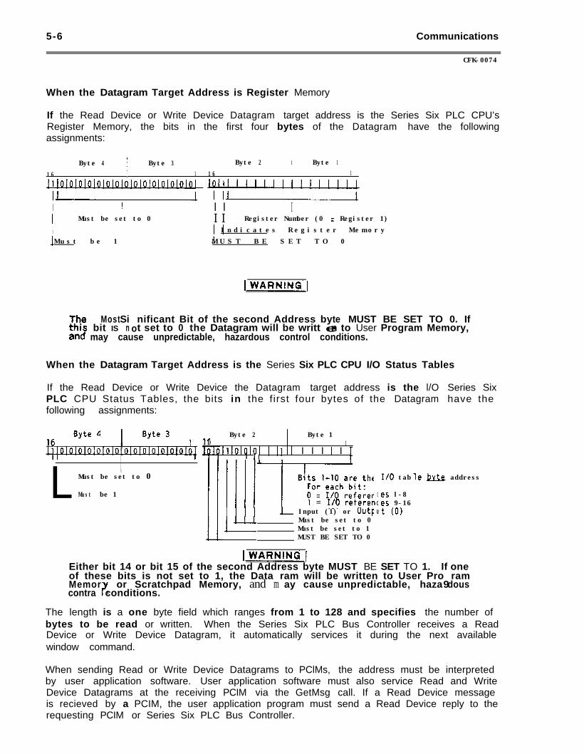
5-6 Communications
CFK-0074
When the Datagram Target Address is Register Memory
If the Read Device or Write Device Datagram target address is the Series Six PLC CPU’sRegister Memory, the bits in the first four bytes of the Datagram have the followingassignments:
Byte 4 1 Byte 3 Byte 2 t Byte 1
1 6 ! 1 1 6 1
Jllolotololol0lololololol0lol0l0l!II I I I I
I Must be set to 0 I I Register Number (0 = Register 1)
t 1 !I n d i c a t e s R e g i s t e r M e m o r y
1M u s t b e 1 JM U S T B E S E T T O 0
Most Sibit IS o
nificant Bit of the second Address byn t set to 0 the Datagram will be writt e
te MUST BE SET TO 0. Ifn to User Program Memory,
may cause unpredictable, hazardous control conditions.
When the Datagram Target Address is the Series Six PLC CPU I/O Status Tables
If the Read Device or Write Device the Datagram target address is the l/O Series SixPLC CPU Status Tables, the bits in the first four bytes of the Datagram have thefollowing assignments:
L tMust be set to 0
Must be 1
Byte 2-e- Byte 1ID 1
Ill0lolol ! !l I I I I I II II
t 1 = I/p referen
It t t t t t I Input (1) or Outf
Must be set to 0Must be set to 1MUST BE SET TO 0
C :es l-8C.es 9-16U t (0)
I/O tablie bvtp address
Either bit 14 or bit 15 of the second Address byte MUST BE SET TO 1.of these bits is not set to 1, the Data
If one
Memor or Scratchpad Memory, andram will be written to User Pro
?m
ram
contra conditions.ay cause unpredictable, haza dous9
The length is a one byte field which ranges from 1 to 128 and specifies the number ofbytes to be read or written. When the Series Six PLC Bus Controller receives a ReadDevice or Write Device Datagram, it automatically services it during the next availablewindow command.
When sending Read or Write Device Datagrams to PClMs, the address must be interpretedby user application software. User application software must also service Read and WriteDevice Datagrams at the receiving PCIM via the GetMsg call. If a Read Device messageis recieved by a PCIM, the user application program must send a Read Device reply to therequesting PCIM or Series Six PLC Bus Controller.
Communications
GFK-0074
5-7
RESPONSE TIME
Since all PCIM services are polled by the Software Driver, response time to a specificPCIM event will for the most part be determined by you and the Host environment. I/Oor Global data response time can be calculated with the formula supplied in the GENIUSI/O Users Manual (GEK-90486). Datagram response time, however, varies with bus scantime, message priority, message length, Bus Controller or PCIM queue loading, andremote CPU sweep time or PC processing delays.
You may wish to optimize response time to certain events though the use of the PCIMinterrupt calls GetlNTR and PutlNTR. See chapter 4 for an example of interrupt coding.
BUS SCAN TIME
Bus scan time, or “token rotation time” is the period of time required for the token tomove completely around the bus, permitting all devices one communications access each.
The maximum bus scan time which can be supported is 400 milliseconds on a bus with noBSM’s attached and 100 milliseconds on a bus with BSM’s attached.
Bus scan time is affected by:
?? the number and types of I/O Blocks
- the number of Bus Controllers, PCIMs, and HHMs
?? amount of Global Data traffic
?? amount of Datagram traffic
?? baud rate
?? single or dual CPU operation
Inputs, outputs and Global data are sent every bus scan.
Datagrams are sent as required by system events, such as faults, logins, HHMcommunications, etc.

5-8 Communications
GFK-0074
As stated, there are two priorities of Datagram transmission - Normal and High. Onlyone device is allowed to send a Normal Priority Datagram per bus scan. Every device cansend a High Priority Datagram each bus scan. So in any one bus scan, there may be up to31 High Priority Datagrams plus one Normal Priority Datagram, or 32 High PriorityDatagrams.
Block fault reports are transmitted as Normal Priority only logins, which automaticallyoccur as a device is initialized, are High Priority Datagrams. Using a Bus Controller orPCIM, you may send a Datagram with either Normal or High priority.
The worst case bus scan time for each GENIUS product is shown in the GENIUS I/O User’sManual (GEK-90486). The numbers shown for each device factor in its number of inputs,outputs, and some of its token passing overhead. Since these numbers are simplified, theactual bus scan time may be slightly less than that shown.
The worst case bus time for the PClM is shown in figure 5-2. A calculation of the totalbus scan time is started by summing the bus scan time contribution for each bus device.Then, add in an “Overhead” period which takes into account some of the token passingoverhead plus communications for the HHM and block faults. If there are no Datagrams,the total bus scan time is the number previously calculated or 3 milliseconds, whicheveris largest.
The following procedure is used to include the impact to bus scan time for Global Dataand Datagrams:
1) Calculate the total number of Global Data bits (number of Global Data bytes X11) transmitted by all PCIMs and Bus Controllers, divide by the baud rate, andadd to the bus scan time.
2) If any PCIMs or Bus Controllers can send user-defined Normal PriorityDatagrams, select the worst case number of data field bits which can be sent byany ONE of these devices (number of data field bytes X 11), then subtract 198.Divide by the baud rate, then add in the resulting time (if negative, add in zero>to the bus scan time.
3) For EACH Bus Controller or PCIM which will send user-defined High PriorityDatagrams, sum the maximum number of data field bits (number of data fieldbytes X 11), then add 55. Divide by the baud rate and add the result into theaccumulated bus scan time.
4) To arrive at the final bus scan time, select either the accumulated total fromstep 3, or 3 milliseconds, whichever is largest.
Product
Bus Time (in ms)
KBaud - - - - 153.6 153.6 76.8 38.4Standard Extended
PCIM 1.00 1.06 2.12 4.25
Figure 5.2 PCIM BUS TIME
Troubleshooting 6-1
CfK-0074
CHAPTER 6TROUBLESHOOTING
INTRODUCTION
This chapter provides the data required for basic troubleshooting and repair should amalfunction of your PCIM occur. Complete troubleshooting information for the GeniusI/O System, Series Six CPU, Series Six Plus CPU, I/O Rack, and Workmaster computercan be found in GEK-90486, GEK-23561A, GEK-96602, and GEK-25373, respectively.
The technology used in the design of the PCIM is such that under normal operatingconditions few hardware failures are expected. If any failures should occur, they canquickly be isolated and the defective assembly replaced with minimum downtime.
As with program debugging, hardware/firmware troubleshooting is accomplished bythinking logically of the function of each part of the system and how these functionsinterrelate. A basic understanding of the various indicator lights will help you quicklyisolate the problem to the PCIM, a Bus Controller, an I/O rack, an I/O Block, or the CPU.
The total system has to be considered when problems occur. The CPU, Host computer,l/O Blocks and external devices connected to or controlled by the GENIUS I/O systemmust all be operating and connected properly. All cable connections as well as allscrew-down or soldered connections should be checked carefully.

6-2 Troubleshooting
TROUBLESHOOTING RESOURCES
The maintenance and troubleshooting section of this manual is designed to help youisolate and correct any problems that may arise in your PCIM. It is recommended that allmaintenance and programming personnel read this section of the manual thoroughly, sothat if a problem does arise, it can be isolated quickly; thus minimizing downtime of thesystem.
However, we realize that troubleshooting isn’t always that simple. Sometimes you needsomeone to talk to who can answer your questions. When you do, first cal I your localauthorized GE Fanuc distributor. After business hours, please don’t hesitate to call theProgrammable Control Emergency Service Number, (804) 978-5747 ( DIAL COMM8-227-5747). An automatic answering device will direct you to the home phone of one ofour Programmable Control Service Personnel. Thus, you are never without backup help.
REPLACEMENT MODULE CONCEPT
The troubleshooting and maintenance techniques described in this manual promote theconcept of complete component replacement.minimize system downtime.
The prime objective of this concept is to
When a problem arises, first isolate it to the major assembly, then to the defectivemodule within that assembly. The defective module is then replaced from a duplicate setof modules maintained on site. Your production line or system is back up fast.
The defective module can be returned through normal channels under warranty or forservice without keeping your production line or system down for an extended period oftime. The replacement concept minimizes downtime to minutes as contrasted(potentially) to days. The potential savings far outweigh the comparatively small cost ofduplicate modules.
If you did not purchase a duplicate set of modules with your initial system, werecommend that you contact your authorized GE Fanuc distributor and do so. Then, withthe help of this manual and the staff of your local authorized GE Fanuc distributor, youwill be able to troubleshoot and repair just about any problem that may arise.
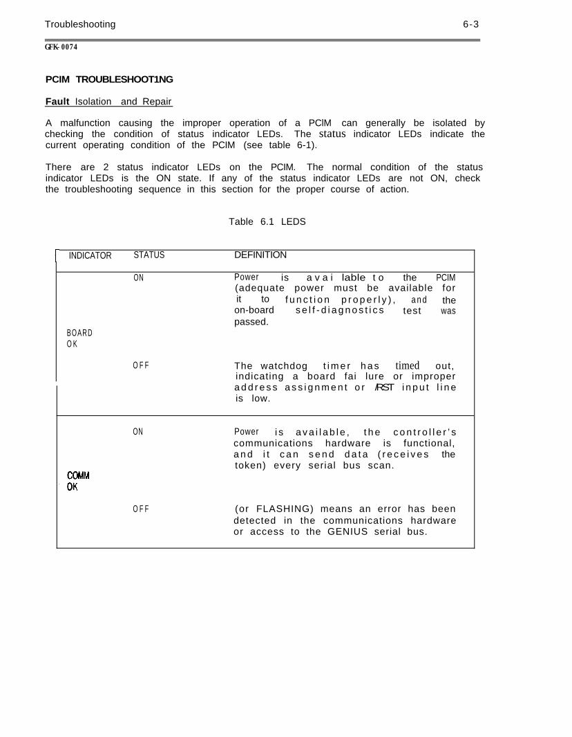
Troubleshooting 6-3
GFK-0074
PCIM TROUBLESHOOT1NG
Fault Isolation and Repair
A malfunction causing the improper operation of a PClM can generally be isolated bychecking the condition of status indicator LEDs. The status indicator LEDs indicate thecurrent operating condition of the PCIM (see table 6-1).
There are 2 status indicator LEDs on the PCIM. The normal condition of the statusindicator LEDs is the ON state. If any of the status indicator LEDs are not ON, checkthe troubleshooting sequence in this section for the proper course of action.
Table 6.1 LEDS
INDICATOR STATUS DEFINITION
ON Power is a v a i lable t o the PCIM
BOARDO K
(adequate power must be available forit to f u n c t i o n p r o p e r l y ) , a n d theon-board s e l f - d i a g n o s t i c s test waspassed.
O F F The watchdog t i m e r h a s timed out,indicating a board fai lure or impropera d d r e s s a s s i g n m e n t o r /RST i n p u t l i n eis low.
ON Power i s a v a i l a b l e , t h e c o n t r o l l e r ’ scommunications hardware is functional,a n d i t c a n s e n d d a t a ( r e c e i v e s thetoken) every serial bus scan.
O F F (or FLASHING) means an error has beendetected in the communications hardwareor access to the GENIUS serial bus.

6-4 Troubleshooting
GFK-0074
If the status indicator LEDs are in the correct state but the bus is not functioningproperly, the malfunctions below may describe the problem. If so, follow the procedureslisted under the appropriate malfunction.
- An LED doesn’t come ON when a PCIM is plugged in and powered up and /RSTinput is high.
If Board OK OFF/Comm OK ON -
Check if dipswitches are set correctly on the I/O rack backplane,motherboard, daughterboard.
If set different then the InitlM parameter, the BOARD OKLED will not come on.
If all appears to be in order, assume hardware failure -replace PCIM.
If Board OK ON/Comm OK OFF -
Check for correct cable type and length (see Genius User’sManual, GEK-90486).
See if correct terminating resistors (see Genius User’s Manual,GEK-90486) are installed at both ends of bus.
Make sure motherboard has JP1 jumper set for appropriate resistor(sent installed).
Determine if serial bus wiring has been completed in a Daisy Chainfashion.
Make sure cabling is not in proximity to high voltage runs.
Look for a broken cable.
If both LEDs off -
Check to see if the PCIM is plugged in, seated properly, andreceiving power.
Check voltage receiving level of /RST. It must remain at 2.4 voltsor higher (TTL logic 1).
If both LEDs flashing together -
Two devices on the same bus have probably been configured withthe same device number (serial bus address).
Check using the HHM.
Troubleshooting
GFK-0074
6-5
- Repeated bus errors
Ensure that cable shielding is properly installed and grounded (seeGenius User’s Manual, GEK-90486).
Unplug bus communications cable from PCIM, refer to the Devicenumber sheets from which you configured the system, and use theHHM to read configuration/compare device numbers and I/Oreference numbers.
If all appears to be in order, replace PCIM.
- System shuts down with parity errors.
Duplicate or overlapping PCIM/I/O References.
Input duplicated on same bus.
Input references from other PClMs overlap.
- Bus Errors - can’t get PCIM up and running
Serial l/Serial 2 crossed
- Intermittent or total lack of communications.
Mixed Baud Rates
Power up blocks one at a time and confirm baud rateAny Change to baud rate in block will not take effectuntil block power is cycled.
- No Global Data.
Destination device off-line
Verify destination on-line.
- Unsuccessful Datagram completion.
Destination device off-line
Verify destination on-line.

Appendix A: Example Application A - l
GFK-0074
APPENDIX AEXAMPLE APPLICATIONS
EXAMPLE APPLICATION 1/*
This programming example uses the InitlM and GetDevConfig functioncalls. Example devices include two PCIMS in a ClMSTAR I connectedto a GENIUS I/O serial bus. The PCIMs have the followingConfigurations (The lMPARMS Structure is defined in PCIM.H):
PCIM #2Serial Bus Address: 30 DecIMPARMS.Segment: DO00 HexIMPARMSIOPort: 3E4 HextMPARMS.IMRef: 3434 HexIMPARMS.OutputLength: 0IMPARMS.InputLength: 0IMPARMS.Act ive: ON
PCIM #1Serial Bus Address: 31 DecIMPARMS.Segment: CC00 HexIMPARMSIOPort: 3E0 HexIMPARMSIMRef: 1212 HexIMPARMSOutputLength: 0tMPARMS.lnputLength: 0IMPARMS.Act ive: ON
These are the only two devices on our example GENIUS bus. TheGetBusConfig function can be used for any device on the bus bygiving the Serial Bus Address of the device desired. If thedevice given is not online, GetDevConfig will return OFFLINE (11).
This example can be built using MicroSof t C Compiler Ver 4.0 or greaterwith the following syntax:
*/
C> MSC gdctst /Zp;C> LINK gdctst, , , pcim;
#include#include
<stdio.h><pcim.h> /* PClM header file */
extern intInitlM( ),ChglMSetup( ),Get DevConf ig( );
IMPARMS local[2]; /* PClM Configuration Structure. . .allocate an elementper PCIM in your PC */
c h a r f lags[2]; /* Error return for PCIM Init. . .allocate anelement per PCIM in your PC. */
DEVI CE conf ig; /* Device Config Structure. . .32 may be al located */

A-2 Appendix A: Example Application
GFK-0074
# d e f i n e PCIM1 &local[0]# d e f i n e PCIM2 &local[l]
/* Macro for easier remembering *//* Macro for easier remembering */
*/
main( )>§
int ret,X,Y,loop=1;
printf("n\n\nCopyright 1987, GE Fanuc Automation North America, Inc.“);printf(“\n\nThis is a test of the GetDevConfig function. . .\n");
printf(“\nTurning on two PCIMs\n\n”);
/* Initialize the PCIM #1 Parameters */tocal[0].im.Segment = OxCCOO;local[0].im.IOPort = Ox3EO;local[0]0]. IMRef = 0x1212;local[0].OutputLength = 0;local[0].lnputLength = 0;local[0].Active = ON;
/* initialize the PCIM #2 Parameters */Iocal[l].im.Segment = OxDOOO;local[l].im.IOPort = Ox3E4;local[l].IMRef = 0x3434;local[l].OutputLength = 0;locai[ll.lnputLength = 0;local[l].Act ive = ON;
if ( (ret = Init IM ( 2, local, flags ) ) != SUCCESS ){
printf(“\nInitlM returned %d\ntest exit”,ret);loop = 0;
}
while(loop){
/*From PCIM #1 (which is SBA 31), GetDevConfig(uration) for SBA 30,which in this case is PCIM #2. This can be used for any deviceson the bus.
*/if ( (ret = GetDevConf ig ( 1, 30, &conf ig) > [= SUCCESS)I
*/
returned an error code...probably 7 or 11 . ..look in PCIM.Hfor Error Return MACROS
printf(‘\nGetDevConf ig returned %d\ntest exit”,ret);loop = 0;
}/*
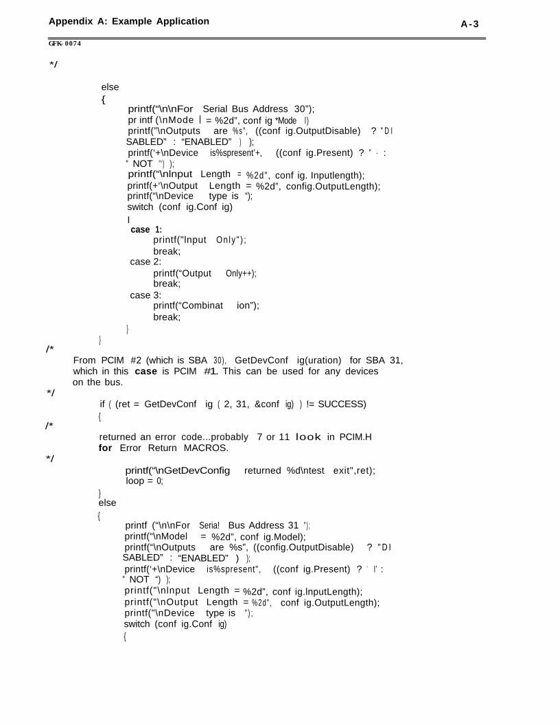
Appendix A: Example Application
GFK-0074
A-3
*/
else{
printf(“\n\nFor Serial Bus Address 30”);pr intf (\nMode I = %2d”, conf ig *Mode l)printf(”\nOutputs are %s" , ((conf ig.OutputDisable) ? " D ISABLED” : “ENABLED” ) );printf(‘+\nDevice is%spresent’+, ((conf ig.Present) ? ” - :
" NOT " ‘ ) );printf(“\nlnput Length = %2d", conf ig. Inputlength);printf(+‘\nOutput Length =printf(“\nDevice type is “);
%2d”, config.OutputLength);
switch (conf ig.Conf ig)Icase 1:
printf("lnput On l y " ) ;break;
case 2:printf(“Output Only++);break;
case 3:printf(“Combinat ion”);break;
}}
/*From PCIM #2 (which is SBA 30) , GetDevConf ig(uration) for SBA 31,which in this case is PCIM #1. This can be used for any deviceson the bus.
*/if ( (ret = GetDevConf ig ( 2, 31, &conf ig) ) != SUCCESS){
/*returned an error code...probably 7 or 11 look in PCIM.Hfor Error Return MACROS.
*/printf(“\nGetDevConfig returned %d\ntest exit",ret);loop = 0;
}else{
printf (“\n\nFor Seria! Bus Address 31 " ) ;printf(“\nModel = %2d”, conf ig.Model);printf(“\nOutputs are %s”, ((config.OutputDisable) ? " D ISABLED” : “ENABLED” ) );printf(‘+\nDevice is%spresent", ((conf ig.Present) ? " I’ :
" NOT “) );printf("\nlnput Length = %2d”, conf ig.lnputLength);printf("\nOutput Length =printf("\nDevice type is " ) ;
%2d" , conf ig.OutputLength);
switch (conf ig.Conf ig){
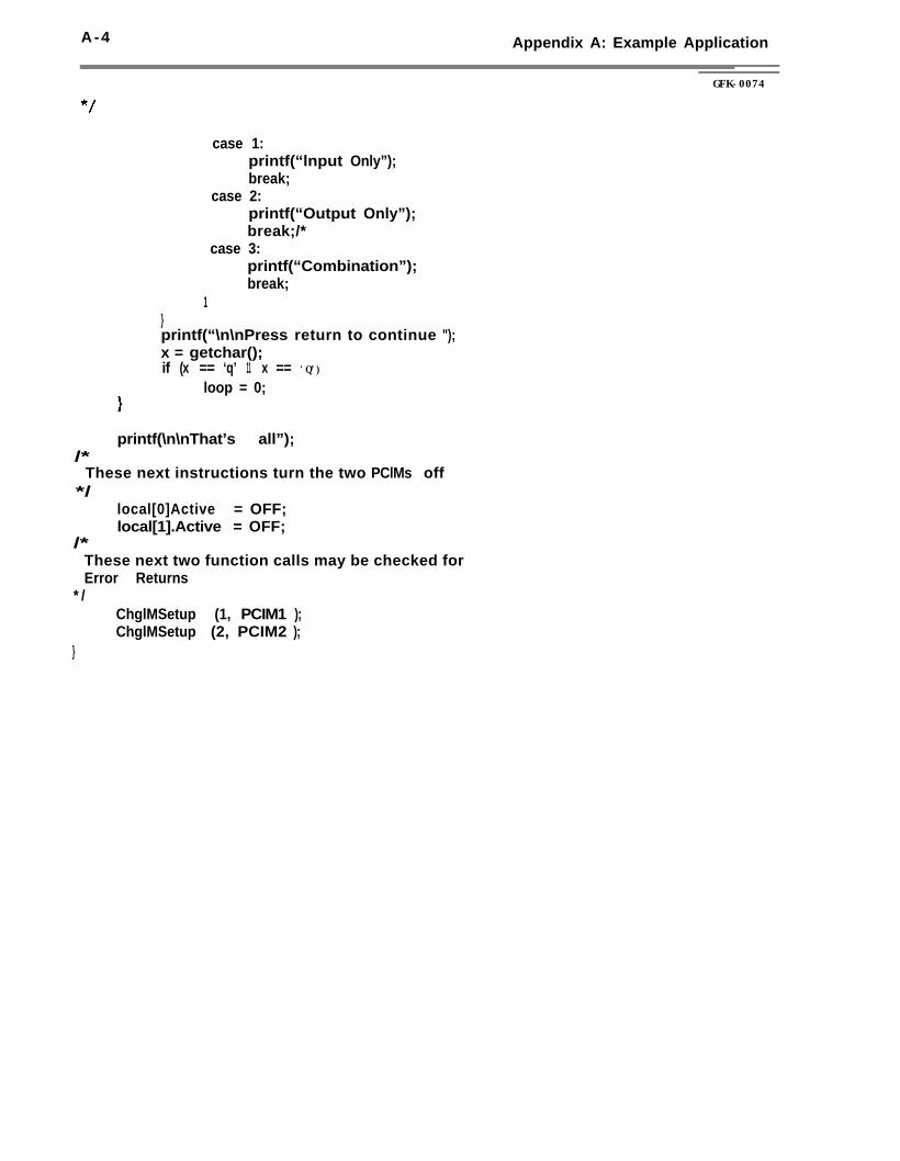
A-4 Appendix A: Example Application
GFK-0074
case 1:printf(“lnput Only”);break;
case 2:printf(“Output Only”);break;/*
case 3:printf(“Combination”);break;
1}printf(“\n\nPress return to continue ");x = getchar();if (x == ‘q’ 11 x == 'Q’)
loop = 0;
printf(\n\nThat’s all”);/*
These next instructions turn the two PClMs off*/
local[0]Active = OFF;local[1].Active = OFF;
/*These next two function calls may be checked forError Returns
* /ChglMSetup (1, PCIM1 );ChglMSetup (2, PCIM2 );
}
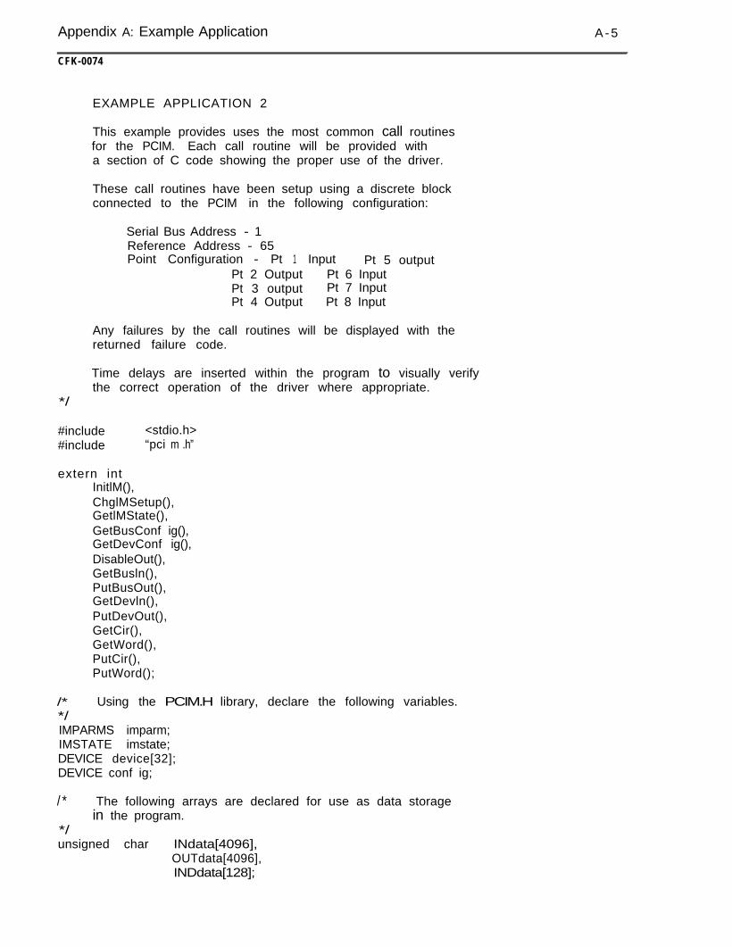
Appendix A: Example Application A - 5
CFK-0074
EXAMPLE APPLICATION 2
This example provides uses the most common call routinesfor the PCIM. Each call routine will be provided witha section of C code showing the proper use of the driver.
These call routines have been setup using a discrete blockconnected to the PCIM in the following configuration:
Serial Bus Address - 1Reference Address - 65Point Configuration - Pt 1 Input Pt 5 output
Pt 2 Output Pt 6 InputPt 3 output Pt 7 InputPt 4 Output Pt 8 Input
Any failures by the call routines will be displayed with thereturned failure code.
Time delays are inserted within the program to visually verifythe correct operation of the driver where appropriate.
*/
#include#include
<stdio.h>“pci m .h”
extern intInitlM(),ChglMSetup(),GetlMState(),GetBusConf ig(),GetDevConf ig(),DisableOut(),GetBusln(),PutBusOut(),GetDevln(),PutDevOut(),GetCir(),GetWord(),PutCir(),PutWord();
/* Using the PCIM.H library, declare the following variables.*/IMPARMS imparm;IMSTATE imstate;DEVICE device[32];DEVICE conf ig;
/ * The following arrays are declared for use as data storagein the program.
*/unsigned char INdata[4096],
OUTdata[4096],INDdata[128];

A - 6 Appendix A: Example Application
GFK-0074
main01
i n t r e t ,
yx = 0 ,
= 0 ,p n u m = 1,d n u m = 1,o f f s e t = 3 ;
c h a r val,valword[1],f l a g s ;
u n s i g n e d c h a r lgth,l e n g t h ;
/* D e f i n e t h e PClM p a r a m e t e r s . T h i s a s s i g n m e n t r e f l e c t s t h e h a r d w a r es e t u p o f t h e PCIM a n d i t s D I P s w i t c h e s .
*/imparm. im.Segment = OxDOOO;imparm. i m . lOPort = Ox3E4;imparm.lMRef = 0 x 0 0 0 0 ;imparm.OutputLength = 0 ;imparm. InputLength = 0 ;imparm.Active = U N ;
/* U s e t h e lnitlM d r i v e r t o i n i t i a l i z e t h e PCIM.* /
f o r ( x=0; x<OxFFF; x t t );i f ( ( r e t = Ini tIM ( p n u m ,{
&imparm, & f l a g s ) ) ! = S U C C E S S )
printf(“\nlnitlM f a i lure, r e t u r n e d %d\n”,ret);}else{
printf(“\nlnitlM d r i v e r successfuI\n”);
f o r ( x=0; x<OxFFFF; x++ )f o r ( y=O; y<0xF; y++);
/ * U s e t h e ChglMSetup d r i v e r to c h a n g e t h e IMREF v a l u e f r o m0 t o 0 x 1 2 1 2 . N o t e t h a t all p a r a m e t e r s i n t h e imparm a r r a yare t r a n s f e r r e d t o t h e PCIM.
* /imparm.lMRef = 0x1212;i f ( ( r e t{
= ChglMSetup ( pnum, &imparm )) ! = S U C C E S S )
printf(“\nChgtMSetup f a i l u r e , r e t u r n e d %d\n”,ret);printf(“\nSegment %x”,imparm.im.Segment);printf(VnIOPort %x”,imparm.im.lOPort);printf(“\nlMRef %d”,imparm.lMRef);printf(“\nOutLength %d”,imparm.OutputLength);printf(“\nlnputLength %d”,imparm.lnputLength);printf(“\nActive %d”, imparm.Act i v e ) ;
}e l s e

Appendix A: Example Application A-7
/*
*/
/*
*/
/*
* /
/**/
printf(“\nOhglMSetup d r i v e r successful\n”);
U s e t h e GetIMState d r i v e r t o r e a d t h e S t a t u s T a b l e a n d S e t u pT a b l e o f t h e PCIM. D i s p l a y t h e D I P S w i t c h v a l u e w h i c h i sr e t u r n e d a s p a r t o f t h i s c a l l .
if (( ret = GetlMState ( p n u m , &imstate) ) ! = S U C C E S S >}
printf(“\nGetlMState f a i l u r e , r e t u r n e d %d\n”,ret ) ;}e l s e{
printf("\nGetlMState d r i v e r successful\n”);printf(” DipSwitch v a l u e %x\n”,imstate.DipSwitch);
U s e t h e G e t B u s C o n f i g d r i v e r t o d i s p l a y t he c o n f i g u r a t i o n o ft h e G e n i u s B u s . D i s p l a y a s u b s e t o f t h e i n f o r m a t i o n r e t u r n e d .
f o r ( x=0; xt0xFFFF; x t t )f o r (y=O; y<OxF; y++);
if (( ret = G e t B u s C o n f i g ( p n u m , d e v i c e ) ) ! = S U C C E S S ){
printf(“\nGetBusConfig f a i l u r e , r e t u r n e d %d\n”, r e t ) ;}e l s e{
}
printf("\nGetBusConfig successful\n);printf(” M o d e l # D e v i c e 1 = %d”, device[1].Model);print f ( ' \n D e v i c e P r e s e n t = %d”, device[1].Present);printf("\n D e v i c e C o n f i g u r a t i o n = %x\n”, device[l].Config);
U s e t h e G e t D e v C o n f i g d r i v e r t o d i s p l a y t h e c o n f i g u r a t i o n o f as p e c i f i c M o c k . D i s p l a y t h e r e f e r e n c e address o f t h e b l o c k .
if (( ret = G e t D e v C o n f i g ( p n u m , d n u m , &config) > ! = S U C C E S S )1
printf(“\nGetDevConf i g f a i l u r e , r e t u r n e d %d\n);}e l s e{
}
printf(“\nGetDevConfig successful\n”);printf(” D e v i c e P r e s e n t = %d”,config.Present);pr intf (“\n D e v i c e r e f e r e n c e a d d r e s s = %d\n”,conf ig.Reference);
U s e t h e P u t C i r d r i v e r t o t u r n o n p t 3 o f t h e G e n i u s I /O block.
for ( x=0 ; x<OxFFFF; x t t )f o r ( y=O; y,0xF; y t t ) ;
if (( ret = PutCir ( pnum, d n u m , o f f s e t , ( c h a r ) 1 ) ) != S U C C E S S )
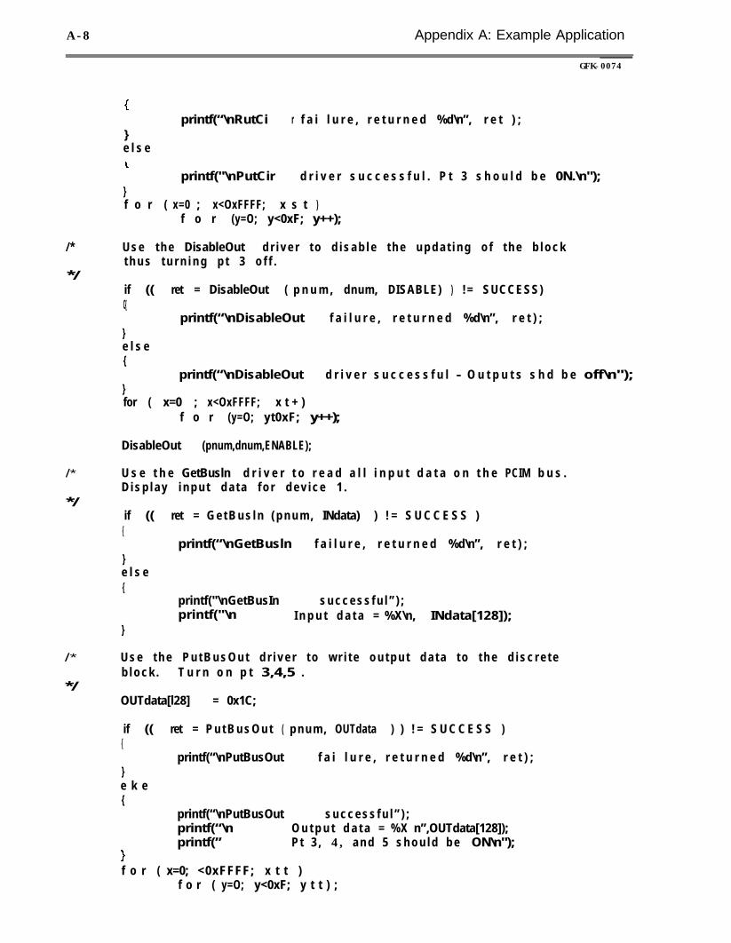
A - 8 Appendix A: Example Application
GFK-0074
printf(“\nRutCi r f a i l u r e , r e t u r n e d %d\n”, r e t ) ;}e l s e
}printf("\nPutCir d r i v e r s u c c e s s f u l . P t 3 s h o u l d b e 0N.\n");
f o r ( x=0 ; x<OxFFFF; x s t )f o r (y=O; y<0xF; y++);
/ * U s e t h e DisableOut d r i v e r t o d i s a b l e t h e u p d a t i n g o f t h e b l o c kt h u s t u r n i n g p t 3 o f f .
*/if (( ret = DisableOut ( p n u m , dnum, DISABLE) ) != SUCCESS)C{
printf(“\nDisableOut f a i l u r e , r e t u r n e d %d\n”, r e t ) ;}e l s e{
}printf(“\nDisableOut d r i v e r s u c c e s s f u l - O u t p u t s s h d b e off\n");
for ( x=0 ; x<OxFFFF; x t + )f o r (y=O; yt0xF; y++);
DisableOut (pnum,dnum,ENABLE);
/* U s e t h e GetBusln d r i v e r t o r e a d a l l i n p u t d a t a o n t h e PCIM b u s .D i s p l a y i n p u t d a t a f o r d e v i c e 1 .
*/if (( ret = G e t B u s l n ( p n u m , INdata) ) ! = S U C C E S S )
{printf(“\nGetBusln f a i l u r e , r e t u r n e d %d\n”, r e t ) ;
}e l s e{
printf("\nGetBusIn s u c c e s s f u l ” ) ;printf("\n I n p u t d a t a = %X\n, INdata[128]);
}
/*
*/
U s e t h e P u t B u s O u t d r i v e r t o w r i t e o u t p u t d a t a t o t h e d i s c r e t eb l o c k . T u r n o n p t 3,4,5 .
OUTdata[l28] = 0x1C;
if (( ret = P u t B u s O u t ( p n u m , OUTdata ) ) ! = S U C C E S S ){
printf(“\nPutBusOut f a i l u r e , r e t u r n e d %d\n”, r e t ) ;}e k e{
printf(“\nPutBusOut s u c c e s s f u l ” ) ;printf(“\n O u t p u t d a t a = %X n”,OUTdata[128]);printf(” P t 3 , 4 , a n d 5 s h o u l d b e ON\n");
f o r ( x=0; <0xFFFF; x t t )f o r ( y=O; y<0xF; y t t ) ;

Appendix A: Example Application A-9
G F K - 0 0 7 4
/*
*/
Use the GetDevln driver to read input data from the discreteblock. V a l u e shouldindicate 0x1C.
if (( ret = GetDevln ( pnum, dnum, &length, INDdata )) != SUCCESS ){t
printf(“\nGetDevln f a i l u r e , r e t u r n e d %d\n”, r e t );}else{
printf(”\nGetDevln Successful”);pr intf (“\n Discrete Block Input Data = %X\n”,lNDdata[0];
/ *
*/
Use the PutDevOut driver to turn on pt 3 and 5 on the discreteblock.
Igth=1;
OUTdata[0]=0x14;
if (( ret = PutDevOut ( pnum, dnum, Igth, OUTdata )) != SUCCESS ){
printf(“\nPutDevOut f a i l u r e , r e t u r n e d %d\n”, r e t ) ;}else{
printf(“\nPutDevOut s u c c e s s f u l ” ) ;printf(“\n Pt 3 and Pt 5 shou Id be ON\n”) ;
/* Use the GetCir and GetWord drivers to read the input status ofthe discrete block.
*/offset = 3;
if (( ret = GetCir ( pnum, dnum, offset, &val)) != SUCCESS ){
printf(“\nGetCir f a i l u r e , r e t u r n e d %d\n”, r e t ) ;}else{
printf(“\nGetCir successfuI");printf(“/n Value read should be 1, vaI= %x/n”, val );
offset = 1;
if (( ret = GetWord ( pnum, dnum, offset, valword)) != SUCCESS ){
printf(“\nGetWord f a i lure, r e t u r n e d %d\n”, r e t ) ;}else
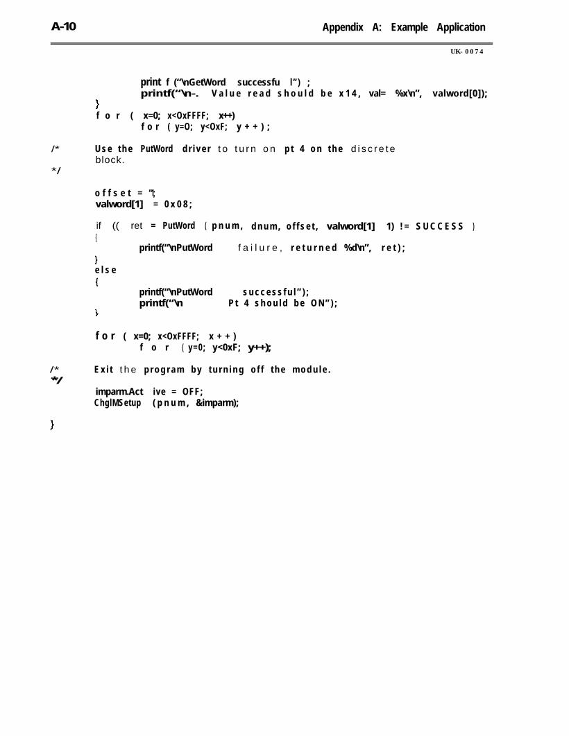
A-10 Appendix A: Example Application
UK-0074
print f (“\nGetWord successfu l ” ) ;printf(“\n-. V a l u e r e a d s h o u l d b e x 1 4 , val= %x\n”, valword[0]);
f o r ( x=0; x<OxFFFF; x++)f o r ( y=O; y<OxF; y + + ) ;
/*
*/
U s e t h e PutWord d r i v e r t o t u r n o n p t 4 o n t h e d i s c r e t eblock.
o f f s e t = “1;valword[1] = 0 x 0 8 ;
if (( ret = PutWord ( p n u m , d n u m , o f f s e t , valword[1] 1) ! = S U C C E S S ){
printf(“\nPutWord f a i l u r e , r e t u r n e d %d\n”, r e t ) ;}e l s e{
printf(“\nPutWord s u c c e s s f u l ” ) ;printf(“\n P t 4 s h o u l d b e O N ” ) ;
f o r ( x=0; x<OxFFFF; x + + )f o r ( y=0; y<0xF; y++);
/* E x i t t h e p r o g r a m b y t u r n i n g o f f t h e m o d u l e .*/
imparm.Act ive = OFF;ChglMSetup ( p n u m , &imparm);
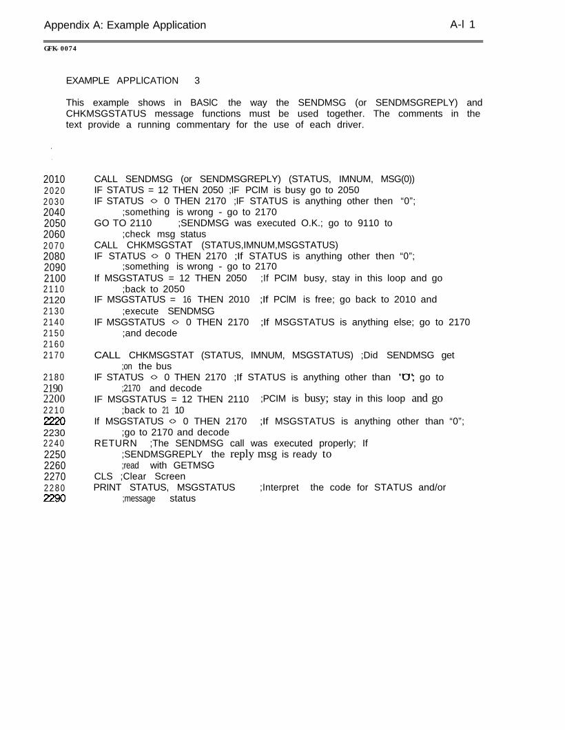
Appendix A: Example Application A-l 1
GFK-0074
EXAMPLE APPLlCATlON 3
This example shows in BASlC the way the SENDMSG (or SENDMSGREPLY) andCHKMSGSTATUS message functions must be used together. The comments in thetext provide a running commentary for the use of each driver.
..
20102 0 2 02 0 3 02040205020602 0 7 02080209021002 1 1 021202 1 3 02 1 4 02 1 5 02 1 6 02 1 7 0
2 1 8 0219022002 2 1 0
22302 2 4 02250226022702 2 8 0
CALL SENDMSG (or SENDMSGREPLY) (STATUS, IMNUM, MSG(0))IF STATUS = 12 THEN 2050 ;IF PCIM is busy go to 2050IF STATUS <> 0 THEN 2170 ;IF STATUS is anything other then “0”;
;something is wrong - go to 2170GO TO 2110 ;SENDMSG was executed O.K.; go to 9110 to
;check msg statusCALL CHKMSGSTAT (STATUS,IMNUM,MSGSTATUS)IF STATUS <> 0 THEN 2170 ;If STATUS is anything other then “0”;
;something is wrong - go to 2170If MSGSTATUS = 12 THEN 2050
;back to 2050;If PCIM busy, stay in this loop and go
IF MSGSTATUS = 16 THEN 2010 ;If PClM is free; go back to 2010 and;execute SENDMSG
IF MSGSTATUS <> 0 THEN 2170 ;If MSGSTATUS is anything else; go to 2170;and decode
CALL CHKMSGSTAT (STATUS, IMNUM, MSGSTATUS) ;Did SENDMSG get;on the bus
IF STATUS <> 0 THEN 2170 ;If STATUS is anything other than "0"; go to;2170 and decode
IF MSGSTATUS = 12 THEN 2110;back to 21 10
;PCIM is busy; stay in this loop and go
If MSGSTATUS <> 0 THEN 2170 ;If MSGSTATUS is anything other than “0”;;go to 2170 and decode
RETURN ;The SENDMSG call was executed properly; If;SENDMSGREPLY the reply msg is ready to;read with GETMSG
CLS ;Clear ScreenPRINT STATUS, MSGSTATUS ;Interpret the code for STATUS and/or
;message status

Appendix B: Glossary B-1
GiK-0074
APPENDIX BGLOSSARY
INTRODUCTION
The following pages present a list of general technical terms used in the body of thismanual. The list includes terms which are presented, but not discussed in detail, inearlier chapters. The list is provided to give you additional information about theseterms. They are listed in alphabetical order followed by their definitions. Technicalterms discussed in detail in the body of this manual are listed in the INDEX.
AC - Acronym for Alternating Current.
A/D Value - Analog to digital. Converts an analog electrical signal into a digital bitpat tern.
Address - A number of groups of ietters and numbers assigned to a specific location inmemory, used to access that location.
Amps (Amperes) - Standard unit of electrical current (MKS system).
- Analoq A numerical expression of physical variables such as rotation and distance torepresent a quantity. Also refers to analog type I/O Blocks and distinguishes them fromdiscrete I/O Blocks.
ASCII (American Standard Code for Information Interchange) - An 8-level code (7 bitsplus 1 parity bit) commonly used for exchange of data.
AWG - Acronym for American Wire Gauge, which defines wire size in O.D.
Background Message - The type of data on the serial bus that is called Background Datain the Serial Bus Specification. This data can be directed to a specific device orbroadcast to all devices.
Battery-backed RAM - A RAM made non-volatile by the addition of a battery to supplydata retention current when main power is gone.
Baud - A unit of transmission speed equal to the number of code elements (bits) persecond.
-Binary A numbering system which uses only the digits 0 and 1. This system is alsocalled a ‘Base Two” numbering system.

B-2 Appendix B: Glossary
GFK-0074
Bit - A contraction of Blnary digiT.numbering system,
The smallest unit of information in the binaryrepresented -by a 0 or 1. The smallest division of a Programmable
Controller “Word”.
BSM - (Bus Selector Module) an external device which selects one of two serial buses forredundancy.
Bus - An electrical path for receiving and transmitting data
Bus Controller - A printed circuit board which provides the interface between theGENIUS l/O system and the Series Six. The Bus Controller f its into any singlehigh-capacity l/O slot and accommodates up to 30 I/O Blocks or Hand Held Monitors.Multiple Bus Controllers can exist without any limit (other than total Series Six I/Ocapacity). The Bus Controller also provides diagnostic fault reporting to the Series Six.
Bus Daisy Chain Configuration - The GENIUS serial bus is a token-passing, pulsetransformer isolated, high-speed (150K baud) link. To connect GENIUS I/O elementstogether is a communications link formed by daisy-chain connection of twisted pair wire.This link requires only one pair.
Bus Scan - a method by which the Bus Controller or Serial Interface monitors all inputsand controls all outputs within a prescribed time. After serving all I/O Blocks and anyadditional HHMs, the token passes to the Bus Controller. The Bus Controller transmitsall outputs and commands from the CPU, then communication begins again with devicezero (or Controller address).
Byte - A group of binary digits (8 bits) that can be used to store a value from 0 to 255.
CPU Sweep - A method by which the CPU scans its associated I/O and solves its logicprogram based on the updated I/O data within a prescribed period of time.
CSB - The Command Status byte of the Command Block.
Communications Controller - A token bus local area network controller which allowsGENIUS l/O devices to communicate over a single shielded twisted wire pair, rather thanvia bundles of point-to-point wires required in conventional systems.
Conf iqure - The act of changing GENIUS I/O system programmable input/output optionsand features initially performed to establish a new configuration different from thoseestablished at the factory. Configuration changes are effected on a block-by-block orcircuit-by-circuit basis, using either the Hand Held Monitor or the Series Six CPU.
Appendix B: Glossary
GFK-0074
B-3
Configuration Data - GENIUS I/O module setup constants.
D/A Value - Digital to analog. Converts a digital bit pattern into a multi-level analogelectrical signal.
DC - Acronym for Direct Current.
DPR Dual Port RAM - the shared RAM interface between the PCIM Manager Softwareand the PCIM Serial Interface.
Datagram Service - A type of data on the serial bus that is described in the NetworkSpecification as Background Data. This data can be directed to a device or broadcast toall devices.
Daughterboard - A PC board that requires another board, called a motherboard, tooperate. A daughterboard is usually mounted on, draws power from and is smaller than amotherboard.
Default - The value, display, function or program automatically selected if the user hasnot specified a choice.
Device Numbers - Each GENIUS device on the bus is assigned a device number (O-31) forcommunications indentif ication. Numbers can be assigned in any order as long as theyare only assigned once per bus.
Digital - Having only two states: ON or OFF.
Dip (Dual lnline Package) Switch - A group of miniature toggle switches arranged side byside in a single package. Commonly used for setting the configuration of variousparameters in electronic equipment.
Discrete - Consisting of individual, distinct entities such as bits, characters, circuits, orcircuit components. Also refers to ON/OFF type I/O Blocks.
EEPROM (Electrically Erasable Programmable Read-Only Memory) - Located within theterminal assembly. The EEPROM stores all user-selectable options and retains theseselections even during power OFF conditions. It can be read by the electronics assemblyat any time and altered by commands from either the CPU or the Hand Held Monitor.

B-4 Appendix B: Glossary
CFK-0074
Electronics Assembly - The part of the I/O Block which contains the power supply,communications chip, microprocessor, smart SW itches, and other electronic componentsrequired to perform GENIUS I/O functions.
Engineering Units - 16-bit 2’s complement numbers supplied by analog I/O Blocks to theSeries Six CPU, or vice-versa. At the analog I/O Block, these are converted to/from the13-bit signed magnitude quantit ies required by the A/D and D/A circuits per theuser-supplied scaling factors.
EPLD - Erasable Programmable Logic Device; an integrated circuit similar to a PALexcept that it is reprogrammable and uses less power.
EPROM - Eraseable Programmable Read-Only Memory device.
Filter - Normally, an electrical circuit designed to eliminate signals of certainfrequencies. In GENIUS l/O Blocks, a programmable digital filter is provided.
FIFO - First In First Out.
Firmware - A series of instructions contained in ROM (Read Only Memory) which areused for internal processing functions only, and thus are transparent to the user.
Foreground tvlessaqe - The type of data on the serial bus that is called Foreground Data inthe Serial Bus Specification. This data can be directed to a specific device or broadcastto all devices.
GENIUS l/O Bus - A high speed serial token passing bus providing communicationsbetween the Bus Controller, Hand Held Monitors, and I/O Blocks. It has high noiseimmunity (1500 volt common mode) and its operation is not affected by any blockattachment, removal or failure. Each data bit is triply encoded for data integrity; errordetection is further improved via cyclical redundancy check (CRC). Bus errors arereported automatically.
Global Data Service - A type of data on the bus that is described in the NetworkSpecification as Control Data. This data can be directed to a specific device orbroadcast to all devices.
Grouped - The 8-circuit Grouped AC l/O Block is so desigated because the l/O circuits allderive power from the block’s power supply.
Appendix B: Glossary B-5
GFK-0074
Hand Held Monitor (HHM) - A portable diagnostic and configuration tool used foraddressing, trouble-shooting, monitoring, scaling and configuring the I/O Bfocks. TheHHM plugs directly into any I/O Block, Bus Controller, or into the Series Six. A keyfeature of the HHM is its ability to manually perform functions and force discrete andanalog I/O, whether or not there is a programmable controller connected to the system.
Hardware - All of the mechanical, electrical, and and electronic devices that comprise aGENIUS I/O system and its application.
Hexadecimal - A base 16 numbering system, represented by the digits 0 through 9 andthen A through F.
High Alarm - A programmable value (in Engineering Units) against which the analog inputsignal is automatically compared on GENlUS I/O Blocks. A fault indication results if theinput value exceeds or equals the high alarm value.
Host - The IBM PC that interfaces to the PCIM’s shared RAM and other connector signals.
HYTX3 - The hybrid circuit that connects directly to the bus transformer on all GENIUSdevices. It is the analog transceiver section of the Serial Interface, providing the analogto digital interface between the tine transformer and the MIT.
PClM MANAGER - The software that controls the flow of data to/from the Host from/tothe serial bus.
l/O - Commonly used abbreviation for Input/Output.
I/O Block - A microprocessor-based, configurable, ruggedized solid state device to whichfield I/O devices are attached. Measuring approximately 9”x4”x3”, it can be mountedvirtually anywhere. No separate rack or power supply is required. Field wiring isattached to a terminal block section which separates from the removable electronicspackage. Due to the microprocessor and intelligent switching, inputs and outputs may bemixed arbitrarily on blocks.
l/O R a c k - 19” Series Six rack which accepts I/O boards, including the GENIUS BusController.
I/O Scan - Each device on the bus has a turn to send information and can listen to all thebroadcast data on the bus. The period required for all devices on the GENIUS bus tocommunicate.
B-6 Appendix B: Glossary
GFK-0074
Impedance - A measure of the total opposition to current flow in an electrical circuit. .
Input - Information originating from an external device.
Input Devices - Devices that as a result of their mechanical or electrical action supplydata to a programmable controller. Typical devices are limit switches, pushbuttons,pressure SW i tches, digital encoders, and analog devices.
Input Processing Time - The time required for input data to reach the microprocessor.
Inrush - Higher than normal currents experienced when output circuits are turned ON.
Isolation - A method of separating field wiring circuitry from logic level circuitry,typically done with optical isolation. Also refers to isolated type I/O Blocks.
ladder Loqic Diagram - A representation of of control logic relay system. Userprogrammed logic is expressed in relay equivalent symbology.
Ladder Logic Programming - A method of solving complex relay problems through the useof simple functions that define or represent relay-oriented concepts.
Low Alarm - A programmable value (in Engineering Units) against which the analog inputsignal is automatically compared on GENIUS I/O Blocks. A fault indication results if theinput value is equal to or less than the low alarm value.
Microsecond (uS) - One millionth of a second (0.000001).
Milliamp (mA) - One 1000th of an ampere.
Millisecond (mS) One thousanth of a second (0.001).
MIT2 - Multiple Interface Timer; This is the Gate Array which implements the hardwareinterface to the serial bus.
Module - In the Series Six, a combination of printed circuit board and its associatedfaceplate which, as a unit, form a complete assembly.

Appendix B: Glossary B-7
GFK-0074
Motherboard - A generic name given to the board that a daughterboard plugs onto.
NVRAM - Non-volatile RAM; The generic term for any RAM that retains its data afterpower loss.
Output - Information traprocesses.
Output Devices - Physicaldata from the programmab
rsferred from the CPU for control of external devices or
devices such as starter motors, solenoids, etc. that receivee control.
Parity - A method of checking the accuracy of binary numbers.
Parity Bit - A bit added to a memory number to make the sum of the 1 bits in a wordalways even (even parity) or always odd (odd parity).
Parity Check - A check that tests whether the number of ones in a word is odd or even.
Peer-to-peer - A system where all devices have the same authority. In contrast, a‘master-slave’ system assumes that the master has all the authority to control datatraffic. A peer-to-peer system allows more flexibility to change configuration, but needsa more complicated method to prevent traffic conflicts,
Private RAM - RAM available only to a specific processor, as differentiated from SharedRAM, which may be available to two or more processors,
Programmable Controller - A solid-state control system which receives inputs fromuser-supplied control devices such as switches and sensors, implements them in a precisepattern determined by instructions stored in user memory, and provides outputs forcontrol of user supplied devices such as relays and starter motors.
PROM - An acronym for Programmable Read Only Memory. A retentive digital storagedevice programmed at the factory and not readily alterable at the field.

B-8 Appendix B: Glossary
GFK-0074
Queue - An architectural construct used to store data in first-in, first-out order. It canbe thought of as a holding area for data, usually equipped with pointers to al low insertionor removal of data.
RAM - An acronym for Random Access Memory. A solid state memory which allowsindividual bits to be stored and accessed. This type of memory is volatile; that is, storeddata is lost under no power conditions. Therefore, a battery backup is required.
Register Reference Number - Memory address of the register used to store 16 bits ofnumerical information such as accumulated or preset times or counts, alarm limits, or thedigital values of an analog output. Registers also may be used to store binaryinformation, such as discrete references.
Serial Bus Address (SBA) - The station number of a device in the GENIUS serial bus tokenrotation scheme.
Serial Bus Scan - The time it takes the token to make one pass around the serial bus.
Serial Communication - A method of data transfer within the GENIUS I/O systemwhereby the bits are handled sequentially, rather than simultaniously as in paralleloperation.
Serial lnterf ace - The software that controls the GENIUS Serial Bus Protocol whichinterfaces the PCIM on the bus.
Series Six CPU (Central Processing Unit) - The central device or controller thatinterprets user instructions, makes decisions based on designated I/O data, and executesthe instructions based on the decisions.
Shared RAM Interface (SRI) : the 16K X 8 SRAM and associated circuitry that arbitratesmemory requests between the PClM and the Host.
Signif icant Bit - A bit that contributes to the precision of a number. The number ofsignificant bits is counted beginning with the bit contributing the most value (referred toas the Most Signif icant Bit (MSB)) and ending with the one contributing the least value(referred to as the Least Significant Bit (LSB)) .
Appendix 8: Glossary
GFK-0074
8-9
Smart Switch - A device with the built-in current and voltage sensors required for theextensive diagnostics available with GENIUS I/O. The Smart Switch allows detection offaults not only within the programmable controller I/O system, but also faults in the coilsand other actuator devices under the control of the programmable controller, as well asthe signal path from pushbuttons and other input devices.
State - ON or OFF condition of current to or from an input or output device.
Steady-State - Signal state after transients have died down.
Table - A group of consecutive registers combined to store data, such as faultinformation.
Terminal Assembly - The part of the I/O Block which is permanently installed. User fieldwiring is connected to the terminal assembly to transmit power and input signals to, andoutput status from the I/O Block.
Termination Jumper - A terminating resistor built into the Bus Controller printed circuitboard, which may be connected to the GENIUS communications bus by moving a jumper(also provided).
Token Passing - The GENIUS I/O bus is a token passing system. Each device on the bushas a turn to send information and can listen to all the broadcast data on the bus. Around robin starts at device zero. While each device holds the token, it can transmitmessages. When complete, the transmitting device sends a sign-off message. If the nexthigher device number is an l/O Block, it sends its input data to all other devices. Lowerdevice numbers are serviced before higher device numbers. Unused device numbers arebypassed with very slight delays.
Volts - The St unit of electric potential and electromotive force.
Watchdog Timer - A hardware timer on firmware-driven systems used to determine thatthe system is meeting certain minimal timing requirements. Shuts the system down in asafe manner if timing requirements fail to be met.
Word - The basic measurement of memory size, which contains 16 bits of information.

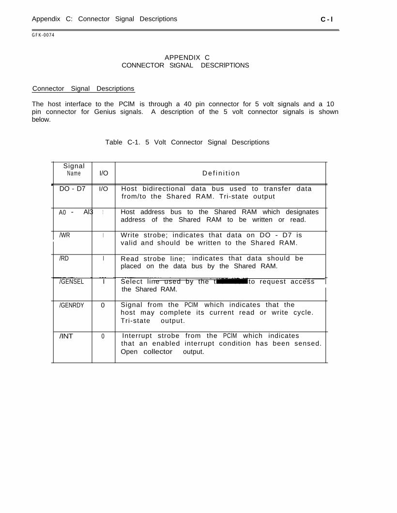
Appendix C: Connector Signal Descriptions
G F K - 0 0 7 4
C - l
APPENDIX CCONNECTOR StGNAL DESCRlPTlONS
Connector Signal Descriptions
The host interface to the PClM is through a 40 pin connector for 5 volt signals and a 10pin connector for Genius signals.below.
A description of the 5 volt connector signals is shown
Table C-1. 5 Volt Connector Signal Descriptions
SignalName I/O D e f i n i t i o n
DO - D7 I/O Host bidirectional data bus used to transfer datafrom/to the Shared RAM. Tri-state output
A0 - Al3 t Host address bus to the Shared RAM which designatesaddress of the Shared RAM to be written or read.
/WR I Write strobe; indicates that data on DO - D7 isvalid and should be written to the Shared RAM.
/RD I Read strobe l ine; indicates that data should beplaced on the data bus by the Shared RAM.
/GENSEL I Select l ine used by the the host to request accessthe Shared RAM.
/GENRDY 0 Signal from the PCIM which indicates that thehost may complete its current read or write cycle.Tri-state output.
/INT 0 Interrupt strobe from the PClM which indicatesthat an enabled interrupt condit ion has been sensed.Open collector output.
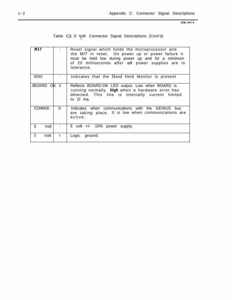
c - 2 Appendix C: Connector Signal Descriptions
GFK-0074
Table C.1 5 Volt Connector Signal Descriptions (Cont’d)-k . .
/RST I Reset signal which holds the microprocessor andthe MIT in reset. On power up or power failure itmust be held low during power up and for a minimumof 20 mill iseconds after all power supplies are intolerance.
MONO t Indicates that the Hand Held Monitor is present
/BOARD OK 0 Reflects BOARD-OK LED output. Low when BOARD isrunning normally. High when a hardware error hasdetected. This l ine is internally current l imitedto 10 ma.
/COMMOK 0 Indicates when communications with the GENIUS busare taking place. It is low when communications area c t i v e .
5 Volt I 5 volt +/- 10% power supply.
0 Volt I Logic ground.
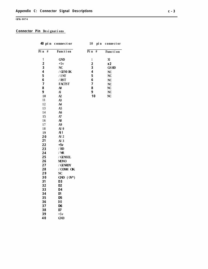
Appendix C: Connector Signal Descriptions c - 3
GFK-0074
Connector Pin Designations
40 pin connector
Pin # Function
10 pin connector
Pin # Function
1 GND2 +5v3 NC4 /GENIOK5 /INT6 /RST7 FACTST8 A09 Al10 A211 A312 A413 A514 A615 A716 A817 A918 Al019 All2 0 Al221 Al32 2 +5v2 3 /RD2 4 /WR2 5 /GENSEL2 6 MONO2 7 /GENRDY2 8 /COMM OK2 9 NC3 0 GND (OV*)31 D33 2 D23 3 D43 4 D13 5 D53 6 D O3 7 D63 8 D73 9 +5v4 0 GND
1 Xl2 x 23 GSHD4 NC5 NC6 NC7 NC8 NC9 NC1 0 NC

Appendix D: Specifications D - l
UK-0074
APPENDIX DSPECIFICATIONS
ELECTRICAL
Power Requirements
5 volts DC +/- 10%, 400 ma (maximum)
Bus Loading
1 LS TTL load per input line
Bus Drive Capability
10 LS TTL loads per output line
All output lines except INTERRUPT are tri-state outputs.
INTERRUPT is an open-collector output.
MECHANICAL
Daughterboard Dimensions
Height - .75” (19.05 mm) (@ tallest component )
Width - 3.6” (91.44 mm)
Depth - 8.4” (213.36 mm)
Board Thickness - .063” (1.60 mm)
Motherboard Dimensions
Height - .75” (19.05 mm) (@ tallest component )
Width - 4.2” (106.68 mm)
Depth - 13.5” (342.9 mm)
Board Thickness - .063” (1 .60 mm)
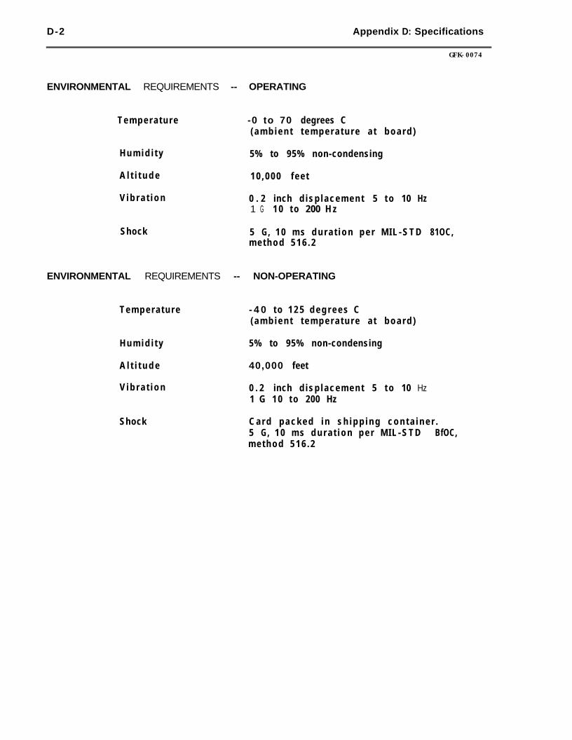
D-2 Appendix D: Specifications
GFK-0074
ENVIRONMENTAL REQUIREMENTS -- OPERATING
T e m p e r a t u r e -0 to 70 degrees C( a m b i e n t t e m p e r a t u r e a t b o a r d )
H u m i d i t y 5% to 95% non-condensing
A l t i t u d e 1 0 , 0 0 0 f e e t
V i b r a t i o n 0 . 2 inch d i s p l a c e m e n t 5 t o 10 Hz1 G 1 0 t o 200 H z
Shock 5 G, 1 0 m s d u r a t i o n p e r M I L - S T D 81OC,m e t h o d 5 1 6 . 2
ENVIRONMENTAL REQUIREMENTS -- NON-OPERATING
T e m p e r a t u r e - 4 0 t o 1 2 5 d e g r e e s C( a m b i e n t t e m p e r a t u r e a t b o a r d )
H u m i d i t y 5% to 95% non-condensing
A l t i t u d e 40,000 feet
V i b r a t i o n 0 . 2 inch d i s p l a c e m e n t 5 t o 10 Hz1 G 1 0 t o 200 Hz
Shock C a r d p a c k e d i n s h i p p i n g c o n t a i n e r .5 G, 1 0 m s d u r a t i o n p e r M I L - S T D BfOC,m e t h o d 5 1 6 . 2
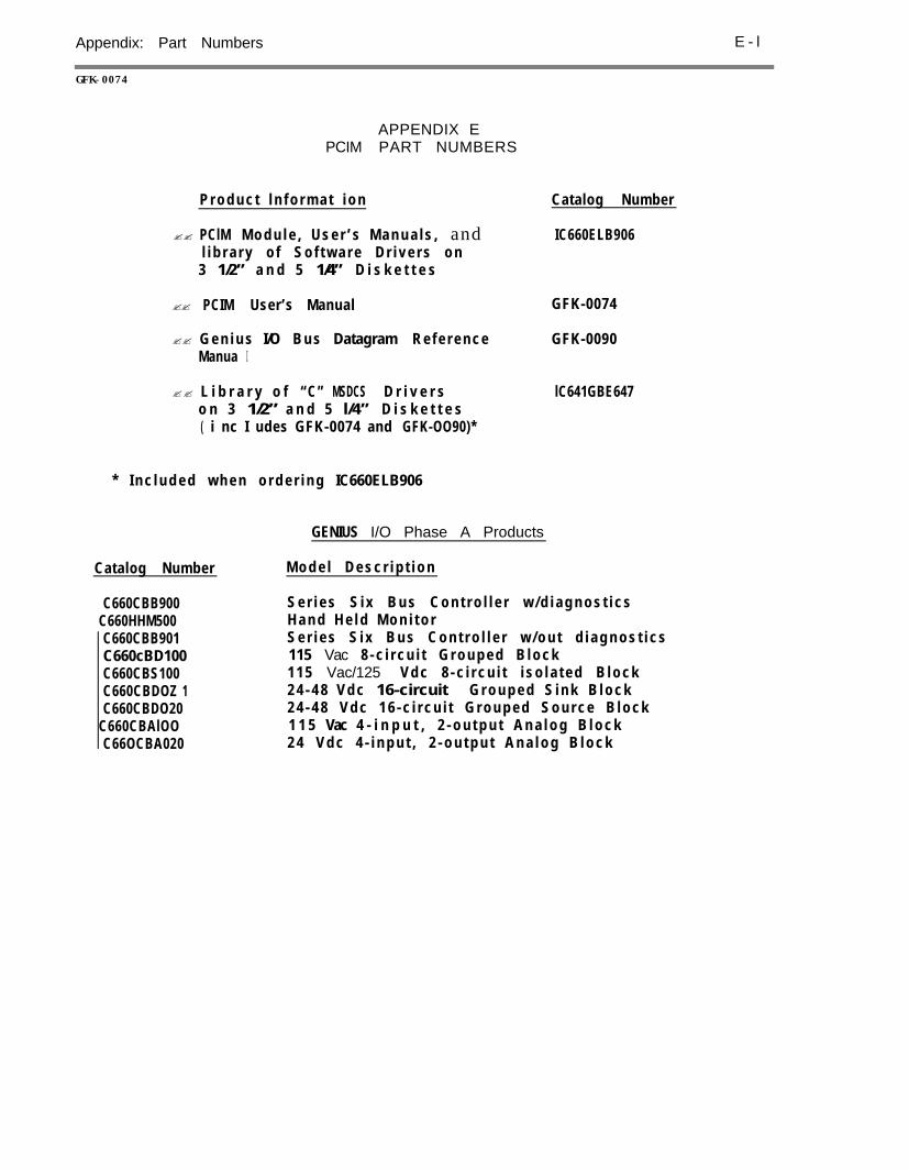
Appendix: Part Numbers E - l
GFK-0074
APPENDIX EPCIM PART NUMBERS
P r o d u c t l n f o r m a t i o n Catalog Number
?? PClM M o d u l e , U s e r ’ s M a n u a l s , andl i b r a r y o f S o f t w a r e D r i v e r s o n3 1/2” a n d 5 1/4” D i s k e t t e s
IC660ELB906
?? PCIM User’s Manual GFK-0074
?? G e n i u s I/O B u s Datagram R e f e r e n c eManua I
GFK-0090
?? L i b r a r y o f “C” MSDCS D r i v e r so n 3 1/2” a n d 5 l/4” D i s k e t t e s( i nc I udes GFK-0074 and GFK-OO90)*
lC641GBE647
* I n c l u d e d w h e n o r d e r i n g IC660ELB906
GENIUS I/O Phase A Products
Catalog Number M o d e l D e s c r i p t i o n
~i C660CBB900C660HHM500C660CBB901C660cBD100C660CBS100C660CBDOZ 1C660CBDO20
C660CBAlOOC66OCBA020
S e r i e s S i x B u s C o n t r o l l e r w / d i a g n o s t i c sH a n d H e l d M o n i t o rS e r i e s S i x B u s C o n t r o l l e r w / o u t d i a g n o s t i c s115 Vac 8 - c i r c u i t G r o u p e d B l o c k1 1 5 Vac/125 V d c 8 - c i r c u i t i s o l a t e d B l o c k2 4 - 4 8 V d c 16-circuit G r o u p e d S i n k B l o c k2 4 - 4 8 V d c 1 6 - c i r c u i t G r o u p e d S o u r c e B l o c k1 1 5 Vac 4 - i n p u t , 2 - o u t p u t A n a l o g B l o c k2 4 V d c 4 - i n p u t , 2 - o u t p u t A n a l o g B l o c k

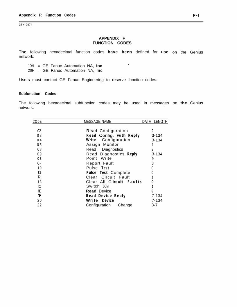
Appendix F: Function Codes
G F K - 0 0 7 4
F - l
APPENDIX FFUNCTION CODES
The following hexadecimal function codes have been defined for usenetwork:
1OH = GE Fanuc Automation NA, Inc20H = GE Fanuc Automation NA, Inc
Users must contact GE Fanuc Engineering to reserve function codes.
Subfunction Codes
The following hexadecimal subfunction codes may be used in messagesnetwork:
C O D E MESSAGE NAME DATA LENGTH
02 Read Configuration 20 3 R e a d Config, w i t h R e p l y 3-1340 4 Write Configuration 3-1340 5 Assign Monitor 10 8 Read Diagnostics 20 9 Read Diagnostics Reply 3-134O B Point Write 9OF Report Fault 31 0 Pulse Test 011 Pulse Test Complete 012 Clear Circuit Fault 11 3 Clear All C ircuit F a u l t s 0IC Switch BSM 11E Read Device 61F R e a d D e v i c e R e p l y 7-1342 0 Write Device 7-1342 2 Configuration Change 3-7
on the Genius
on the Genius

Index I - l
CFK-0074
A
ADDRESSING 3-3Motherboard Memory Map 3-3
Segment Addressing 3-3I/O Port Addressing 3-3
Motherboard Dip SW itchS e t t i n g s 3 - 4
SW1 - I/O Base StartingAddress 3-4
SW2 and SW3 - Host MemoryAddress 3-5
S W 4 3 - 6Daughterboard Dip Switch
Settings 3-6Application Example 3-10Setting Dip Switches
Example 3-l 1Appendix A: Example
Appl icat ions A - lAppendix B: Glossary B-lAppendix C: Connector Signal
Descriptions C-lConnector Pin
Designat ions C-2Appendix D: Specifications
E l e c t r i c a l D - lPower Requirements D-lBus Loading D-lBus Drive Capabi t i ty D - l
M e c h a n i c a l D - lDaughterboard Dimensions D-lMotherboard Dimensions D-l
Environmental Requirements -Operating D-2
Environmental Requirements -Non-Operating D-2
Appendix E: Part Numbers E - lAppendix F: Function Codes F - lApplication Example 3-10Architecture, Genius I/O
S y s t e m 1 - 2
Basic Data Array Structures 4-60Basic Driver Installat ion 4-59Basic Driver Function Calls,
Coding 4-67
INDEX
Basic Driver Function CallParameters 4-59
Basic Driver Function CallPresentation 4-68
Basic Language PCIMSoftware Driver 4-59Bus Scan Time 5-7Bus Termination, Jumpers, and
Resistors 3-2
C
ChglMSetup 4-16,72ChkMsgStat 4 - 5 3 , 1 0 7C Software Driver Installation 4-4C Software Driver Function Call
Parameters 4-5Communications 5-1Communications Cable 3-l 2Compiling Your Applications with
M i c r o s o f t 4 - 4Connector, HHM 3-15
D
Data Buffer 2-5Data Paths, Global 5-2Data, Types of 5-1
Global Data 5-1Datagram D a t a 5 - 3
Datagram Service 5-3Datagram Target Address: Register
M e m o r y 5 - 6Datagram Target Address: Series I/O
Status Tables 5-6Daughterboard Physical Structure,
PCIM 2 - lDevice Configuration Table 2-l 8Device I/O Table 2-17Device Log In 2-14Device Log Out 2-14Dip Switch Settings 3-5Dip Switches, Setting, Example 3-11Directed Control Input Table,
PCIM 2 - 1 8DisableOut 4 - 2 5
l-2 fndex
E
Electrical Character istics 2-22
F
Faceplate Marking 3-15Function Cal I Parameters,
Soft ware Driver 4-3,59Function Call Presentation,
Software Driver 4-7,68Function Cal Is, Soft ware
D r i v e r 4 - l ,59
G
GENIUS l/O IBM PC Interface Module(PCIM) Daughterboard 1-3
GENIUS I/O IBM PC Interface Module(PCIM) Motherboard 1-3
GENIUS I/O System Overview l - lGetBusConf ig 4-21
Get DevConf ig 4-23,77GetBusln 4-27,82GetCir 4-38,94GetDevh 4-31,86GetlMln 4-35,90GetlMState 4-19,74Getlntr 4-55,111GetMsg 4 - 4 6 , 1 0 9Getting Started 3-1
Introduction 3-1Hardware Required 3-lSoftware Required 3-1Bus Termination, Jumpers and
Resistors 3-2Addressing 3-3Communications Cable 3-l 2PCIM Installation 3-13PClM Startup Software 3-14HHM Connector 3-15Faceplate Marking 3-l 5
GetWord 4-42,98
l-l
Hardware Description, PCIM 2-lHardware Operation, PCIM 2-3Hardware Required 3-l
GFK-0074
HHM Connector 3-15Host Interface 2-6Host Operating System 4-lHost System Interrupt Control 2-21
I
lnitltM 4 - 1 3Input Table 2-17I/O Space 3-4I/O Table, Device 2-17l/O Table Lockout 2-17Interrupt Tables 2-l 9
J
Jumpers JP1 and JP2 3-2
L
Language 4-1LEDs 6 - 2
M
Memory Space 3-5Memory Configuration 2-14Motherboard Memory Map 3-3
0
Operation, Theory of 2-lOutput Table 2-17
P
PClM Block Diagram 2-13PClM Broadcast Control Output
T a b l e 2 - 1 8PCIM Directed Control Input
Table 2-f 8PCIM Hardware Description 2-1
PCIM Motherboard PhysicalStructure 2-1
PCIM Daughterboard PhysicalS t r u c t u r e 2 - l
PCIM Hardware Operation 2-3Serial Interface 2-3Data Buffer 2-5Host Interface 2-6
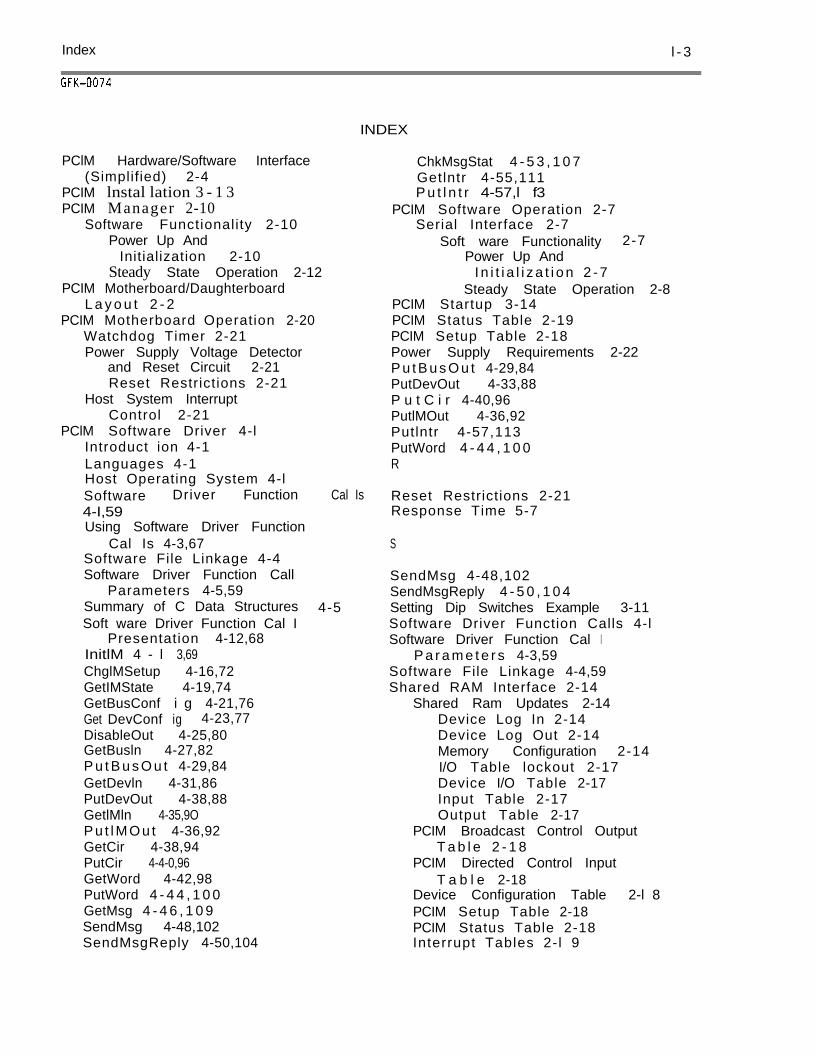
Index l - 3
PClM Hardware/Software Interface(Simplified) 2-4
PCIM lnstal lation 3 - 1 3PCIM Manager 2-10
Software Functionality 2-10Power Up And
Initialization 2-10Steady State Operation 2-12
PCIM Motherboard/DaughterboardL a y o u t 2 - 2
PCIM Motherboard Operation 2-20
INDEX
ChkMsgStat 4 - 5 3 , 1 0 7Getlntr 4-55,111P u t l n t r 4-57,l f3
PCIM Software Operation 2-7Serial Interface 2-7
Soft ware Functionality 2-7Power Up And
I n i t i a l i z a t i o n 2 - 7Steady State Operation 2-8
PCIM Startup 3-14PCIM Status Table 2-19PCIM Setup Table 2-18Power Supply Requirements 2-22P u t B u s O u t 4-29,84PutDevOut 4-33,88P u t C i r 4-40,96PutlMOut 4-36,92Putlntr 4-57,113PutWord 4 - 4 4 , 1 0 0R
Watchdog Timer 2-21Power Supply Voltage Detector
and Reset Circuit 2-21f Reset Restrictions 2-21
Host System InterruptControl 2-21
PClM Software Driver 4-lIntroduct ion 4-1Languages 4-1Host Operating System 4-lSoftware Driver Function4-I,59Using Software Driver Function
Cal Is 4-3,67Software File Linkage 4-4Software Driver Function Call
Parameters 4-5,59Summary of C Data StructuresSoft ware Driver Function Cal I
Presentation 4-12,68InitlM 4 - l 3,69ChglMSetup 4-16,72GetIMState 4-19,74GetBusConf i g 4-21,76Get DevConf ig 4-23,77DisableOut 4-25,80GetBusln 4-27,82P u t B u s O u t 4-29,84GetDevln 4-31,86PutDevOut 4-38,88GetlMln 4-35,9OP u t l M O u t 4-36,92GetCir 4-38,94PutCir 4-4-0,96GetWord 4-42,98PutWord 4 - 4 4 , 1 0 0GetMsg 4 - 4 6 , 1 0 9SendMsg 4-48,102SendMsgReply 4-50,104
Cal Is Reset Restrictions 2-21Response Time 5-7
S
4-5
SendMsg 4-48,102SendMsgReply 4 - 5 0 , 1 0 4Setting Dip Switches Example 3-11Software Driver Function Calls 4-lSoftware Driver Function Cal I
P a r a m e t e r s 4-3,59Software File Linkage 4-4,59Shared RAM Interface 2-14
Shared Ram Updates 2-14Device Log In 2-14Device Log Out 2-14Memory Configuration 2-14I/O Table lockout 2-17Device I/O Table 2-17Input Table 2-17Output Table 2-17
PCIM Broadcast Control OutputT a b l e 2 - 1 8
PCIM Directed Control InputT a b l e 2-18
Device Configuration Table 2-l 8PCIM Setup Table 2-18PCIM Status Table 2-18Interrupt Tables 2-l 9
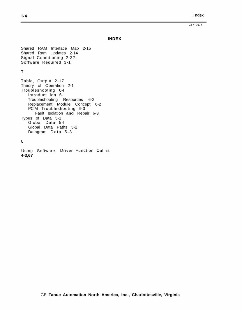
l-4 I ndex
G F K - 0 0 7 4
INDEX
Shared RAM Interface Map 2-15Shared Ram Updates 2-14Signal Conditioning 2-22Software Required 3-1
T
Table, Output 2-17Theory of Operation 2-1Troubleshooting 6-I
Introduct ion 6-lTroubleshooting Resources 6-2Replacement Module Concept 6-2PCIM Troubleshooting 6-3
Fault Isolation and Repair 6-3Types of Data 5-1
Global Data 5-lGlobal Data Paths 5-2Datagram D a t a 5 - 3
U
Using Software Driver Function Cal is4-3,67
GE Fanuc Automation North America, Inc., Charlottesville, Virginia