GC03 Logic gates and Transistors - winddoing.github.io · H1-GC03 Logic Gates & Transistors 14 0V...
40
28/10/2012 H1-GC03 Logic Gates & Transistors 1 GC03 Logic gates and Transistors Peter Rounce [email protected]
Transcript of GC03 Logic gates and Transistors - winddoing.github.io · H1-GC03 Logic Gates & Transistors 14 0V...
28/10/2012H1-GC03 Logic Gates &
Transistors1
GC03 Logic gates and Transistors
Peter [email protected]
28/10/2012H1-GC03 Logic Gates &
Transistors2
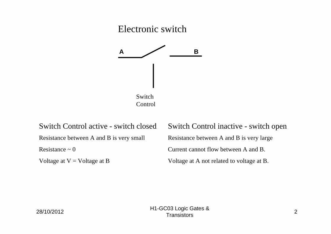
Switch Control
BA
Switch Control active - switch closed
Resistance between A and B is very small
Resistance ~ 0
Voltage at V = Voltage at B
Switch Control inactive - switch open
Resistance between A and B is very large
Current cannot flow between A and B.
Voltage at A not related to voltage at B.
Electronic switch
28/10/2012H1-GC03 Logic Gates &
Transistors3
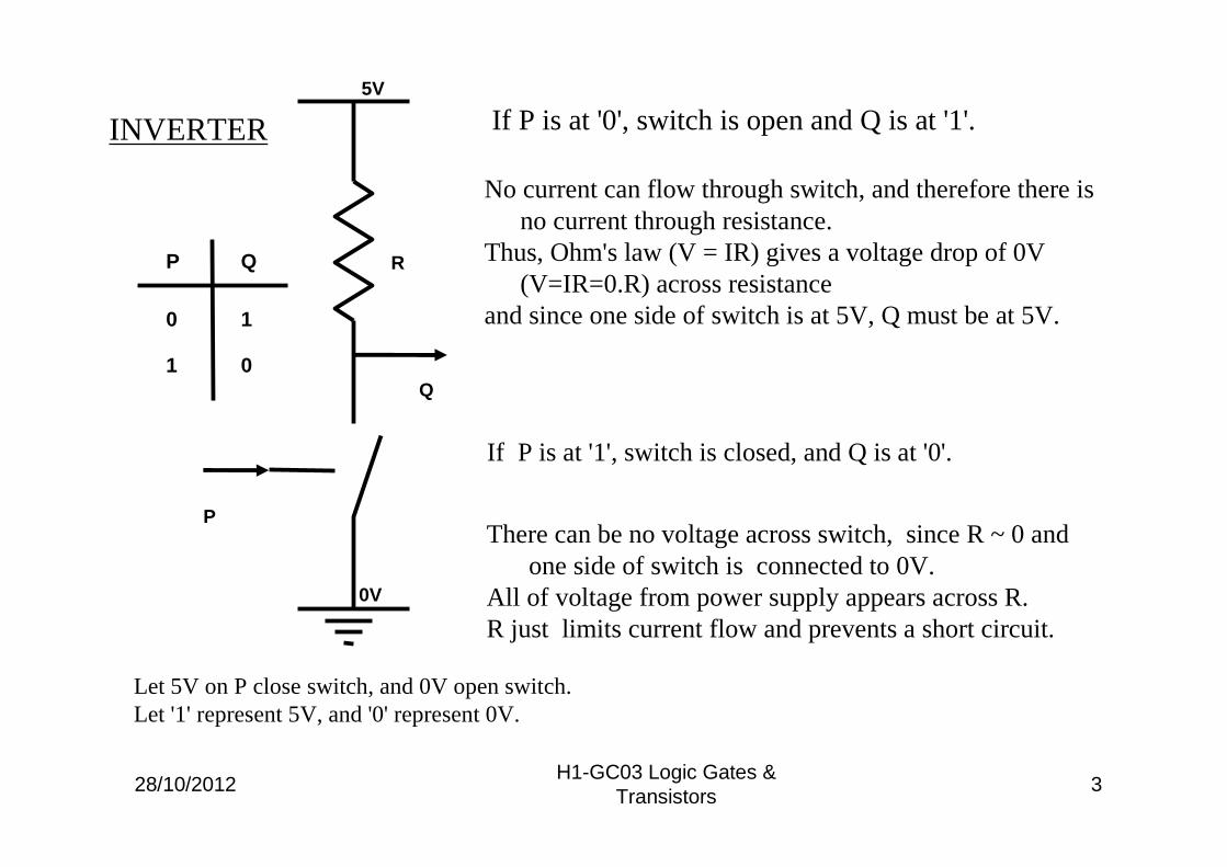
P Q
0
1 0
1
R
P
Q
0V
5V
No current can flow through switch, and therefore there is no current through resistance.
Thus, Ohm's law (V = IR) gives a voltage drop of 0V (V=IR=0.R) across resistance
and since one side of switch is at 5V, Q must be at 5V.
If P is at '0', switch is open and Q is at '1'.
There can be no voltage across switch, since R ~ 0 and one side of switch is connected to 0V.
All of voltage from power supply appears across R.R just limits current flow and prevents a short circuit.
If P is at '1', switch is closed, and Q is at '0'.
INVERTER
Let 5V on P close switch, and 0V open switch.Let '1' represent 5V, and '0' represent 0V.
28/10/2012H1-GC03 Logic Gates &
Transistors4
111
01010
1
00A B C
1
Truth Table
Circuit symbol for 2-input nand
3-input nand
R
A
B
C
5V
0V A B A.B A.B
0 0 0 10 1 0 11 0 0 11 1 1 0
Truth table for nand
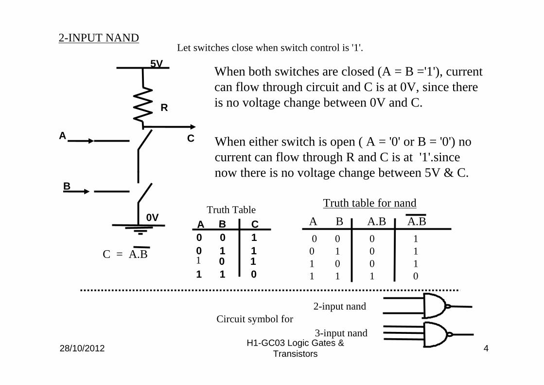
Let switches close when switch control is '1'.
When both switches are closed (A = B ='1'), current can flow through circuit and C is at 0V, since there is no voltage change between 0V and C.
When either switch is open ( A = '0' or B = '0') no current can flow through R and C is at '1'.since now there is no voltage change between 5V & C.
2-INPUT NAND
C = A.B
28/10/2012H1-GC03 Logic Gates &
Transistors5
0011
0101
1010
1100
000011
11
D E F H10000000
Truth Table
R
FED
H
5V
0V0V 0V
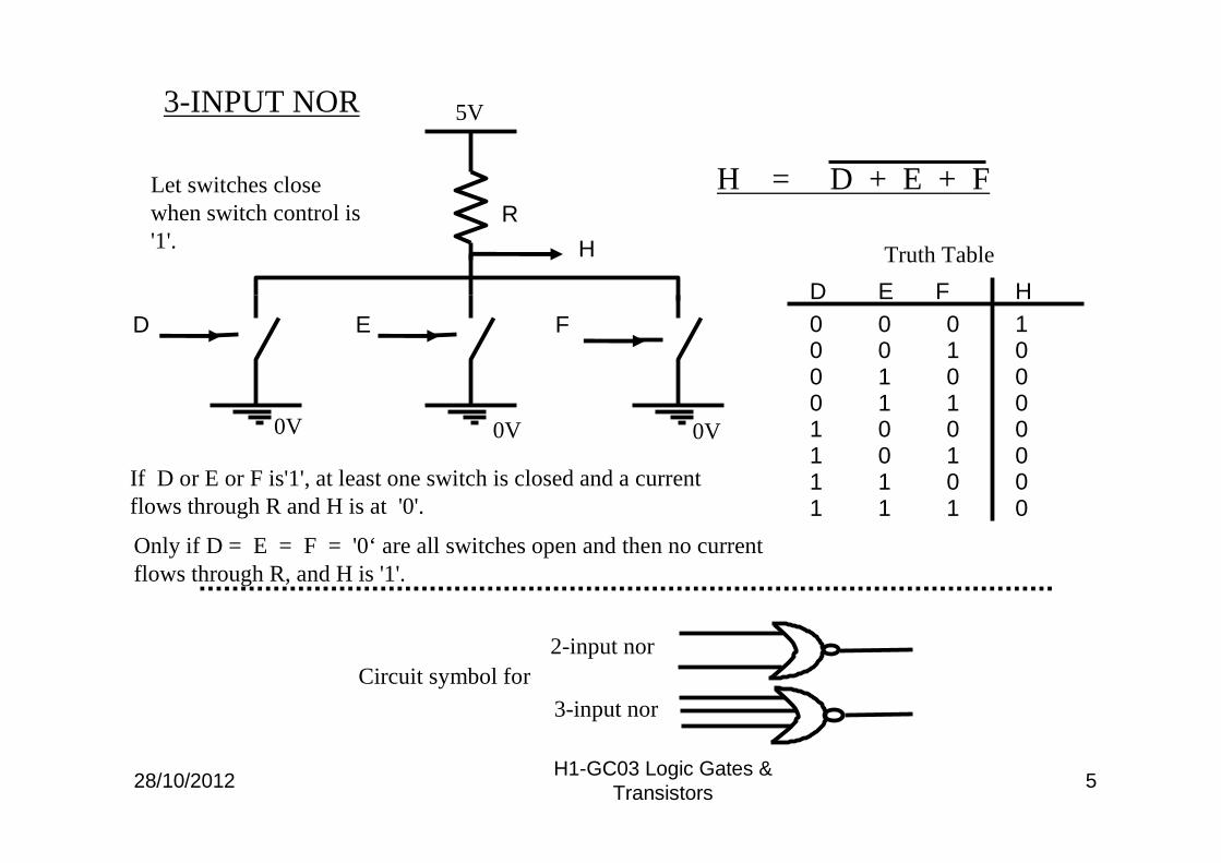
Let switches close when switch control is '1'.
3-INPUT NOR
If D or E or F is'1', at least one switch is closed and a current flows through R and H is at '0'.
Only if D = E = F = '0‘ are all switches open and then no current flows through R, and H is '1'.
2-input nor
3-input nor
Circuit symbol for
H = D + E + F
28/10/2012H1-GC03 Logic Gates &
Transistors6
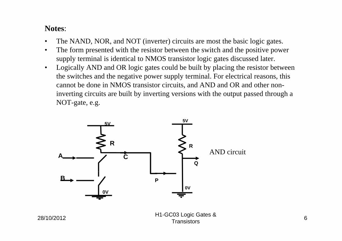
Notes:
• The NAND, NOR, and NOT (inverter) circuits are most the basic logic gates.• The form presented with the resistor between the switch and the positive power
supply terminal is identical to NMOS transistor logic gates discussed later.• Logically AND and OR logic gates could be built by placing the resistor between
the switches and the negative power supply terminal. For electrical reasons, this cannot be done in NMOS transistor circuits, and AND and OR and other non-inverting circuits are built by inverting versions with the output passed through a NOT-gate, e.g.
R
A
B
C
5V
0V
R
P
Q
0V
5V
AND circuit
28/10/2012H1-GC03 Logic Gates &
Transistors7
Metals - an electron is released by each metal atom to form a free electron `soup'.Applying an electric field across metal moves free electrons: a current flows.
Insulators - atoms in insulators keep all their electrons firmly attached.No electron 'soup' is created, and no current will flow in response to an applied electric field.
Semiconductors: these are normally weakly conducting when pure, conduction can be increased by 'doping': adding other materials.
Silicon doped with phosphorus atoms produces an n-type material:n-types semiconductors: electrons carry current.
Silicon doped with boron atoms produces a p-type material:p-type semiconductors: 'holes' carry current.
Materials
28/10/2012H1-GC03 Logic Gates &
Transistors8
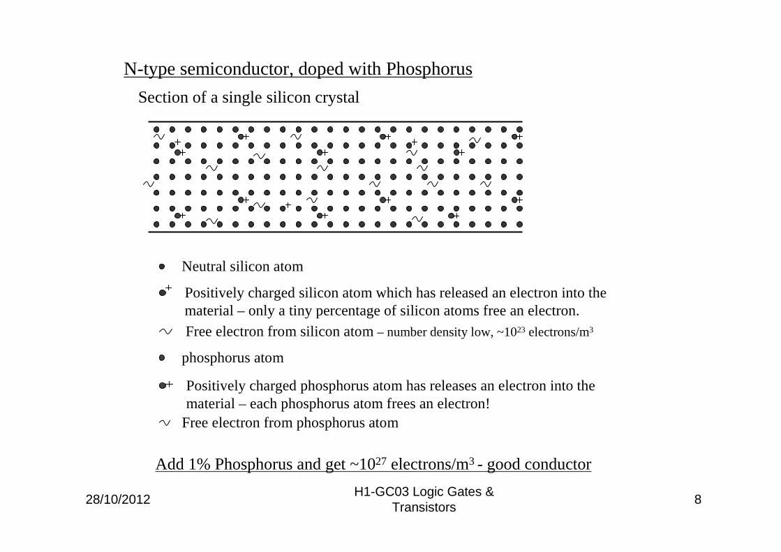
Neutral silicon atom
Positively charged silicon atom which has released an electron into the material – only a tiny percentage of silicon atoms free an electron.
Free electron from silicon atom – number density low, ~1023 electrons/m3
N-type semiconductor, doped with Phosphorus
Section of a single silicon crystal
phosphorus atom
Positively charged phosphorus atom has releases an electron into the material – each phosphorus atom frees an electron!
Free electron from phosphorus atom
Add 1% Phosphorus and get ~1027 electrons/m3 - good conductor
28/10/2012H1-GC03 Logic Gates &
Transistors9
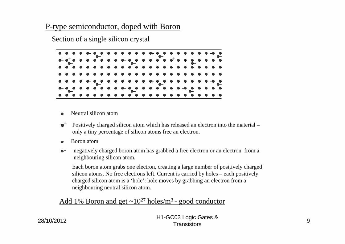
Neutral silicon atom
Positively charged silicon atom which has released an electron into the material –only a tiny percentage of silicon atoms free an electron.
P-type semiconductor, doped with Boron
Section of a single silicon crystal
Boron atom
negatively charged boron atom has grabbed a free electron or an electron from a neighbouring silicon atom.
Add 1% Boron and get ~1027 holes/m3 - good conductor
Each boron atom grabs one electron, creating a large number of positively charged silicon atoms. No free electrons left. Current is carried by holes – each positively charged silicon atom is a ‘hole’: hole moves by grabbing an electron from a neighbouring neutral silicon atom.
28/10/2012H1-GC03 Logic Gates &
Transistors10
+++
+
+
+
++
++
++
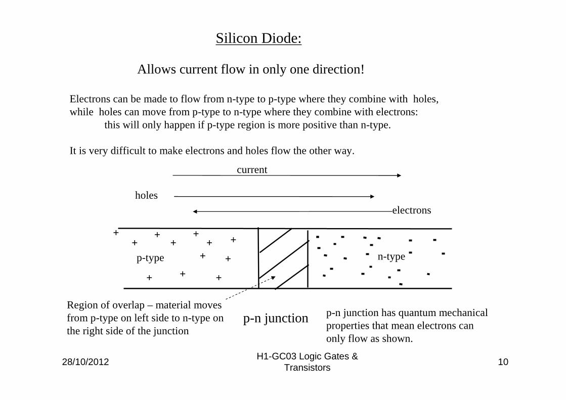
holes
current
electrons
n-typep-type
p-n junction
Allows current flow in only one direction!
Electrons can be made to flow from n-type to p-type where they combine with holes, while holes can move from p-type to n-type where they combine with electrons:
this will only happen if p-type region is more positive than n-type.
It is very difficult to make electrons and holes flow the other way.
Silicon Diode:
Region of overlap – material moves from p-type on left side to n-type on the right side of the junction
p-n junction has quantum mechanical properties that mean electrons can only flow as shown.
28/10/2012H1-GC03 Logic Gates &
Transistors11
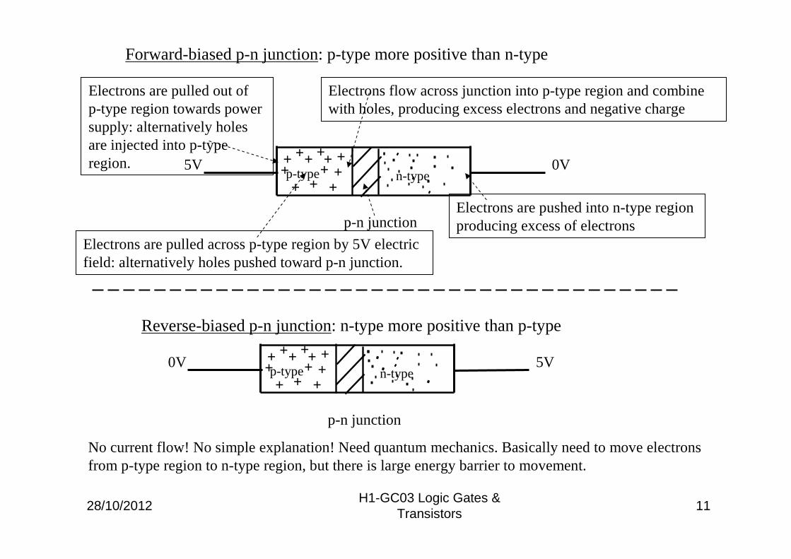
+++++
+++++
++
n-typep-type
p-n junction
0V 5V
+++++
+++++
++
n-typep-type
p-n junction
5V 0V
Forward-biased p-n junction: p-type more positive than n-type
Electrons are pushed into n-type region producing excess of electrons
Electrons flow across junction into p-type region and combine with holes, producing excess electrons and negative charge
Electrons are pulled across p-type region by 5V electric field: alternatively holes pushed toward p-n junction.
Electrons are pulled out of p-type region towards power supply: alternatively holes are injected into p-type region.
Reverse-biased p-n junction: n-type more positive than p-type
No current flow! No simple explanation! Need quantum mechanics. Basically need to move electrons from p-type region to n-type region, but there is large energy barrier to movement.
28/10/2012H1-GC03 Logic Gates &
Transistors12
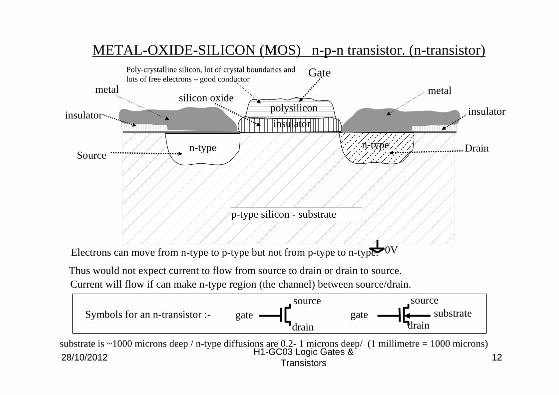
p-type silicon - substrate
Electrons can move from n-type to p-type but not from p-type to n-type.
Thus would not expect current to flow from source to drain or drain to source.Current will flow if can make n-type region (the channel) between source/drain.
polysilicon
n-typen-type
insulator
silicon oxide
Gate
0V
SourceDrain
metal metal
METAL-OXIDE-SILICON (MOS) n-p-n transistor. (n-transistor)
substrate is ~1000 microns deep / n-type diffusions are 0.2- 1 microns deep/ (1 millimetre = 1000 microns)
gatesource
draingate
source
drainsubstrateSymbols for an n-transistor :-
insulator insulator
Poly-crystalline silicon, lot of crystal boundaries and lots of free electrons – good conductor
28/10/2012H1-GC03 Logic Gates &
Transistors13
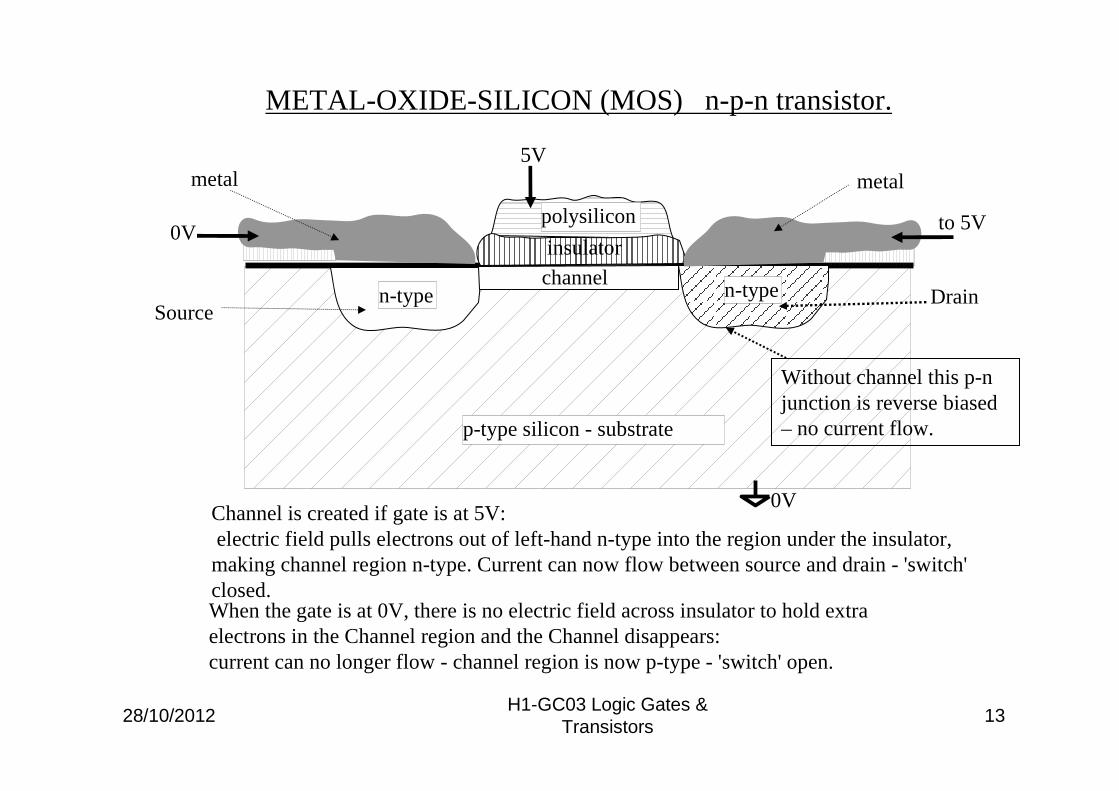
p-type silicon - substrate
polysilicon
n-typen-type
insulator
0V
SourceDrain
metal metal
channel
METAL-OXIDE-SILICON (MOS) n-p-n transistor.
Channel is created if gate is at 5V:electric field pulls electrons out of left-hand n-type into the region under the insulator, making channel region n-type. Current can now flow between source and drain - 'switch' closed.When the gate is at 0V, there is no electric field across insulator to hold extra electrons in the Channel region and the Channel disappears:current can no longer flow - channel region is now p-type - 'switch' open.
0V to 5V
5V
Without channel this p-njunction is reverse biased – no current flow.
28/10/2012H1-GC03 Logic Gates &
Transistors14
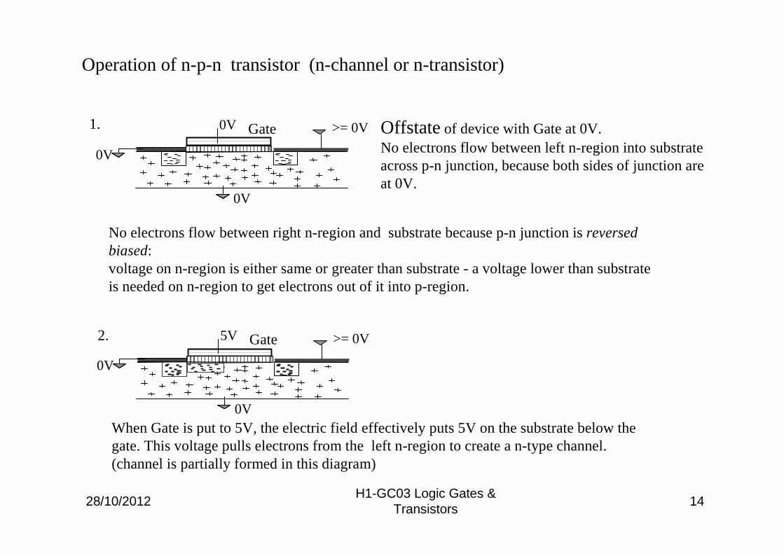
0V
>= 0V
0V
Gate0V1.
0V
>= 0V
0V
Gate5V2.
When Gate is put to 5V, the electric field effectively puts 5V on the substrate below the gate. This voltage pulls electrons from the left n-region to create a n-type channel. (channel is partially formed in this diagram)
Operation of n-p-n transistor (n-channel or n-transistor)
Offstateof device with Gate at 0V.No electrons flow between left n-region into substrate across p-n junction, because both sides of junction are at 0V.
No electrons flow between right n-region and substrate because p-n junction is reversed biased: voltage on n-region is either same or greater than substrate - a voltage lower than substrate is needed on n-region to get electrons out of it into p-region.
28/10/2012H1-GC03 Logic Gates &
Transistors15
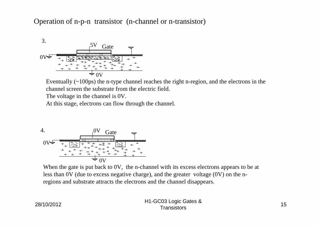
Operation of n-p-n transistor (n-channel or n-transistor)
Eventually (~100ps) the n-type channel reaches the right n-region, and the electrons in the channel screen the substrate from the electric field. The voltage in the channel is 0V. At this stage, electrons can flow through the channel.
0V
0V
Gate5V3.
0V
0V
Gate0V4.
When the gate is put back to 0V, the n-channel with its excess electrons appears to be at less than 0V (due to excess negative charge), and the greater voltage (0V) on the n-regions and substrate attracts the electrons and the channel disappears.
28/10/2012H1-GC03 Logic Gates &
Transistors16
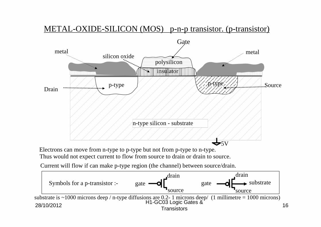
n-type silicon - substrate
Electrons can move from n-type to p-type but not from p-type to n-type.Thus would not expect current to flow from source to drain or drain to source.
Current will flow if can make p-type region (the channel) between source/drain.
polysilicon
p-typep-type
insulator
silicon oxide
Gate
5V
DrainSource
metal metal
METAL-OXIDE-SILICON (MOS) p-n-p transistor. (p-transistor)
substrate is ~1000 microns deep / n-type diffusions are 0.2- 1 microns deep/ (1 millimetre = 1000 microns)
gatesource
draingate
source
drainsubstrateSymbols for a p-transistor :-
28/10/2012H1-GC03 Logic Gates &
Transistors17
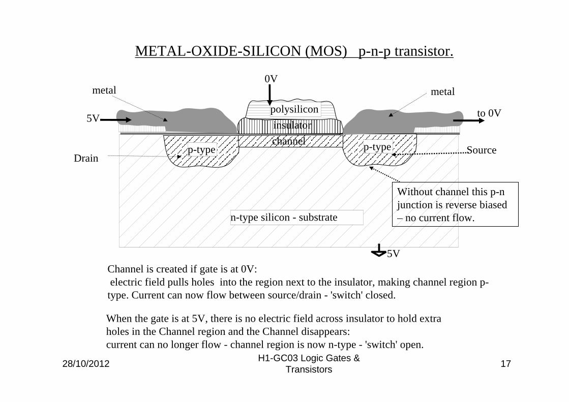
n-type silicon - substrate
polysilicon
p-typep-type
insulator
5V
DrainSource
metal metal
Channel is created if gate is at 0V:electric field pulls holes into the region next to the insulator, making channel region p-type. Current can now flow between source/drain - 'switch' closed.
channel
METAL-OXIDE-SILICON (MOS) p-n-p transistor.
When the gate is at 5V, there is no electric field across insulator to hold extra holes in the Channel region and the Channel disappears:current can no longer flow - channel region is now n-type - 'switch' open.
5V to 0V
0V
Without channel this p-njunction is reverse biased – no current flow.
28/10/2012H1-GC03 Logic Gates &
Transistors18
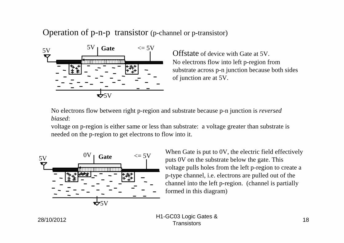
5V <= 5V5V
5V
Gate
When Gate is put to 0V, the electric field effectively puts 0V on the substrate below the gate. This voltage pulls holes from the left p-region to create a p-type channel, i.e. electrons are pulled out of the channel into the left p-region. (channel is partially formed in this diagram)
Offstateof device with Gate at 5V. No electrons flow into left p-region from substrate across p-n junction because both sides of junction are at 5V.
No electrons flow between right p-region and substrate because p-n junction is reversed biased: voltage on p-region is either same or less than substrate: a voltage greater than substrate is needed on the p-region to get electrons to flow into it.
Operation of p-n-p transistor (p-channel or p-transistor)
0V <= 5V5V
5V
Gate
28/10/2012H1-GC03 Logic Gates &
Transistors19
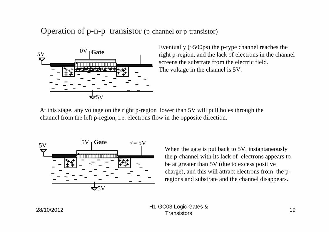
At this stage, any voltage on the right p-region lower than 5V will pull holes through the channel from the left p-region, i.e. electrons flow in the opposite direction.
0V5V
5V
Gate
Operation of p-n-p transistor (p-channel or p-transistor)
Eventually (~500ps) the p-type channel reaches the right p-region, and the lack of electrons in the channel screens the substrate from the electric field. The voltage in the channel is 5V.
When the gate is put back to 5V, instantaneously the p-channel with its lack of electrons appears to be at greater than 5V (due to excess positive charge), and this will attract electrons from the p-regions and substrate and the channel disappears.
5V <= 5V5V
5V
Gate
28/10/2012H1-GC03 Logic Gates &
Transistors20
Input
5V
0V
Output
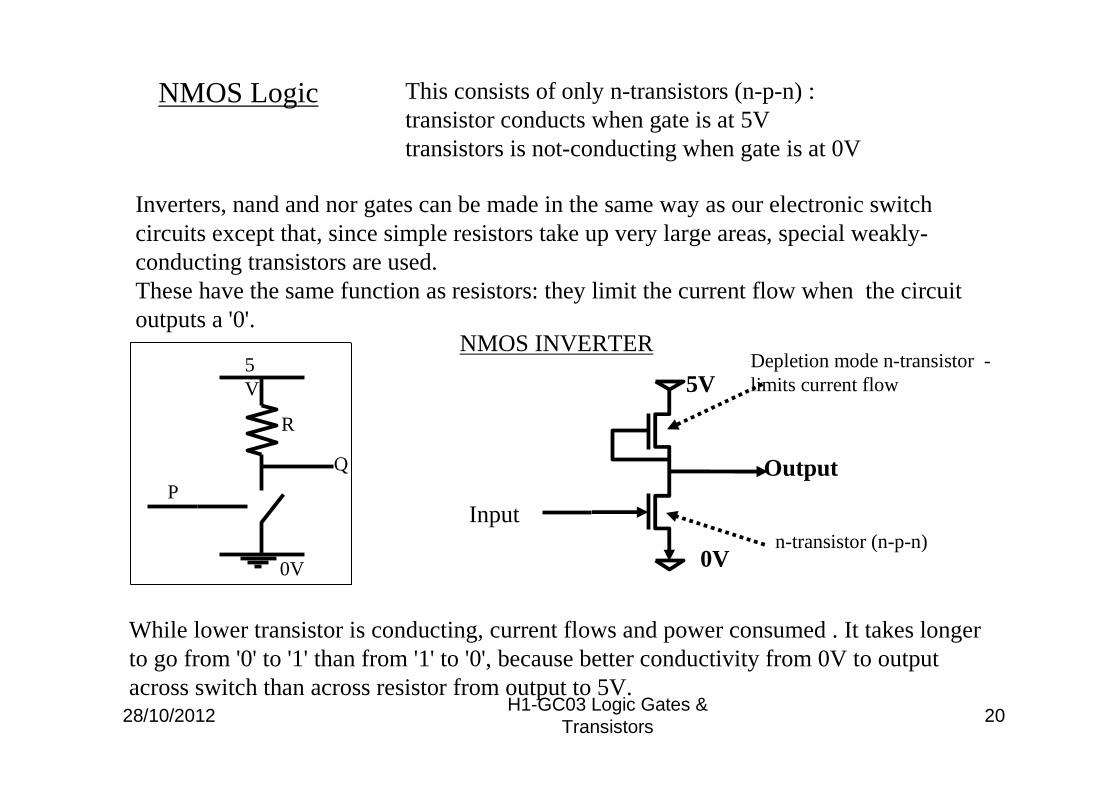
Inverters, nand and nor gates can be made in the same way as our electronic switch circuits except that, since simple resistors take up very large areas, special weakly-conducting transistors are used. These have the same function as resistors: they limit the current flow when the circuit outputs a '0'.
NMOS Logic This consists of only n-transistors (n-p-n) :transistor conducts when gate is at 5Vtransistors is not-conducting when gate is at 0V
NMOS INVERTER
n-transistor (n-p-n)
Depletion mode n-transistor -limits current flow
While lower transistor is conducting, current flows and power consumed . It takes longer to go from '0' to '1' than from '1' to '0', because better conductivity from 0V to output across switch than across resistor from output to 5V.
P
R
Q
0V
5V
28/10/2012H1-GC03 Logic Gates &
Transistors21
B
5V
0V
A C
R
R
H
5V
0V0V 0V
E FD
2-INPUT NAND
3-INPUT NOR
5V
C
B
A
0V
R
NMOS
R
H
5V
0V0V 0V
E FD
NMOS
28/10/2012H1-GC03 Logic Gates &
Transistors22
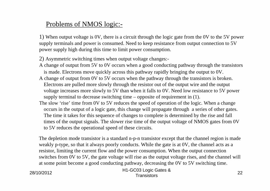
Problems of NMOS logic:-
1) When output voltage is 0V, there is a circuit through the logic gate from the 0V to the 5V power supply terminals and power is consumed. Need to keep resistance from output connection to 5V power supply high during this time to limit power consumption.
2) Asymmetric switching times when output voltage changes:-A change of output from 5V to 0V occurs when a good conducting pathway through the transistors
is made. Electrons move quickly across this pathway rapidly bringing the output to 0V.A change of output from 0V to 5V occurs when the pathway through the transistors is broken.
Electrons are pulled more slowly through the resistor out of the output wire and the output voltage increases more slowly to 5V than when it falls to 0V. Need low resistance to 5V power supply terminal to decrease switching time – opposite of requirement in (1).
The slow ‘rise’ time from 0V to 5V reduces the speed of operation of the logic. When a change occurs in the output of a logic gate, this change will propagate through a series of other gates. The time it takes for this sequence of changes to complete is determined by the rise and fall times of the output signals. The slower rise time of the output voltage of NMOS gates from 0V to 5V reduces the operational speed of these circuits.
The depletion mode transistor is a standard n-p-n transistor except that the channel region is made weakly p-type, so that it always poorly conducts. While the gate is at 0V, the channel acts as a resistor, limiting the current flow and the power consumption. When the output connection switches from 0V to 5V, the gate voltage will rise as the output voltage rises, and the channel will at some point become a good conducting pathway, decreasing the 0V to 5V switching time.
28/10/2012H1-GC03 Logic Gates &
Transistors23
Inverter 5V
0V
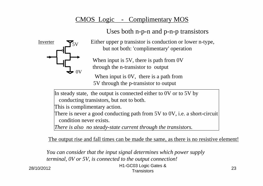
CMOS Logic - Complimentary MOS
Either upper p transistor is conduction or lower n-type, but not both: 'complimentary' operation
When input is 5V, there is path from 0V through the n-transistor to output
When input is 0V, there is a path from 5V through the p-transistor to output
In steady state, the output is connected either to 0V or to 5V by conducting transistors, but not to both.
This is complimentary action.There is never a good conducting path from 5V to 0V, i.e. a short-circuit
condition never exists.There is also no steady-state current through the transistors.
Uses both n-p-n and p-n-p transistors
You can consider that the input signal determines which power supply terminal, 0V or 5V, is connected to the output connection!
The output rise and fall times can be made the same, as there is no resistive element!
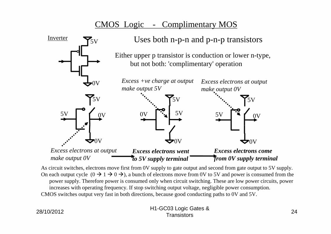
28/10/2012H1-GC03 Logic Gates &
Transistors24
Inverter5V
0V
CMOS Logic - Complimentary MOS
Either upper p transistor is conduction or lower n-type, but not both: 'complimentary' operation
As circuit switches, electrons move first from 0V supply to gate output and second from gate output to 5V supply.On each output cycle (0 � 1 � 0 �), a bunch of electrons move from 0V to 5V and power is consumed from the
power supply. Therefore power is consumed only when circuit switching. These are low power circuits, power increases with operating frequency. If stop switching output voltage, negligible power consumption.
CMOS switches output very fast in both directions, because good conducting paths to 0V and 5V.
Uses both n-p-n and p-n-p transistors
5V
0V
5V 0V
Excess electrons at output make output 0V
5V
0V
0V 5V
Excess +ve charge at output make output 5V
Excess electrons went to 5V supply terminal
5V
0V
5V 0V
Excess electrons at output make output 0V
Excess electrons come from 0V supply terminal
28/10/2012H1-GC03 Logic Gates &
Transistors25
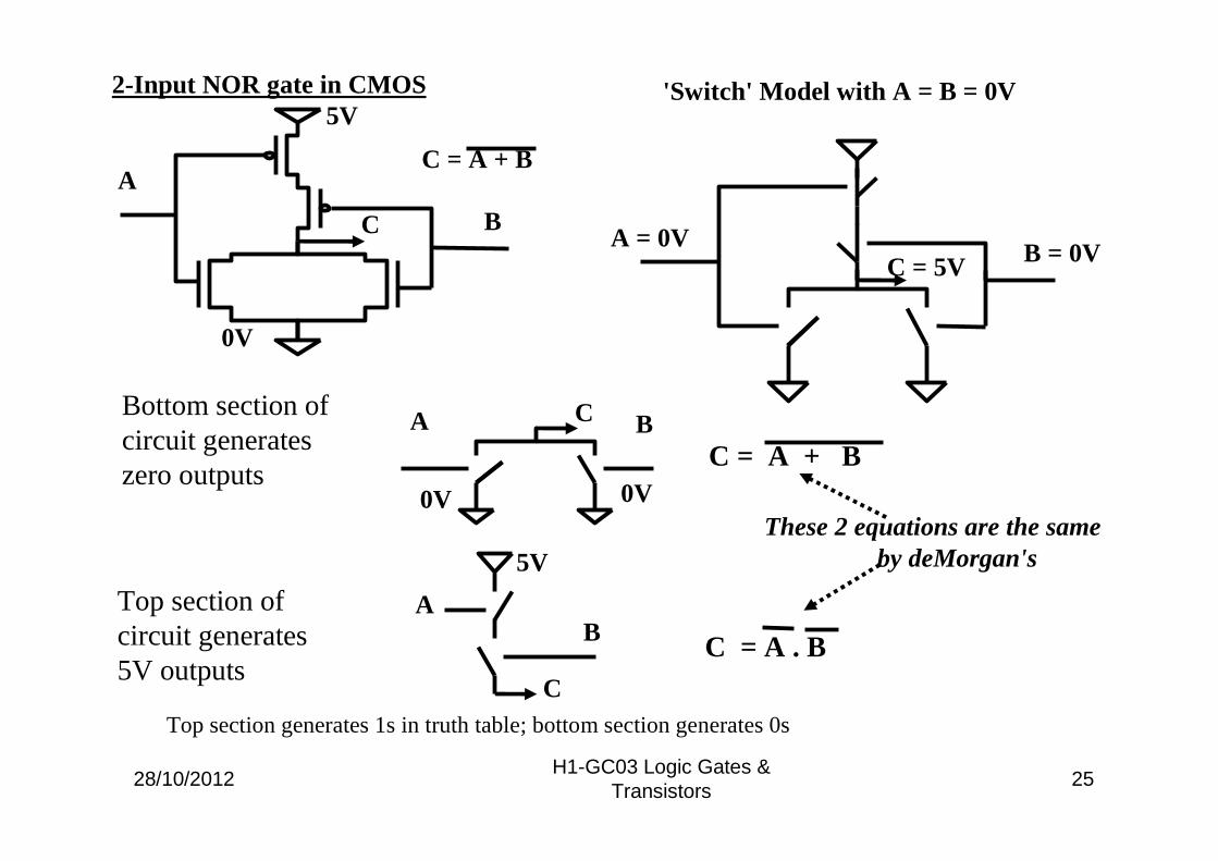
C = A + B
C BA
0V0V
AB
5V
C
2-Input NOR gate in CMOS
C = A + B
5V
BC
A
0V
'Switch' Model with A = B = 0V
A = 0VB = 0VC = 5V
Bottom section ofcircuit generateszero outputs
Top section ofcircuit generates5V outputs
C = A . B
These 2 equations are the same by deMorgan's
Top section generates 1s in truth table; bottom section generates 0s
28/10/2012H1-GC03 Logic Gates &
Transistors26
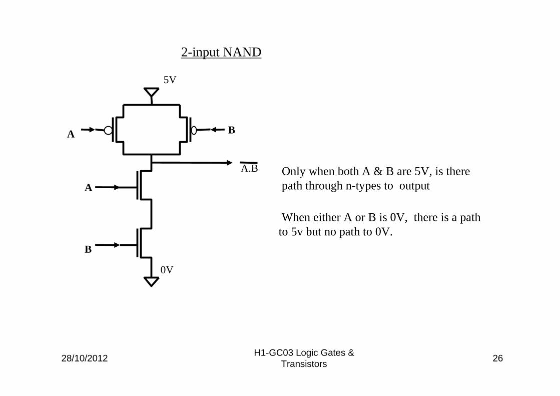
A
A
B
B
0V
5V
A.B Only when both A & B are 5V, is there path through n-types to output
When either A or B is 0V, there is a path to 5v but no path to 0V.
2-input NAND
28/10/2012H1-GC03 Logic Gates &
Transistors27
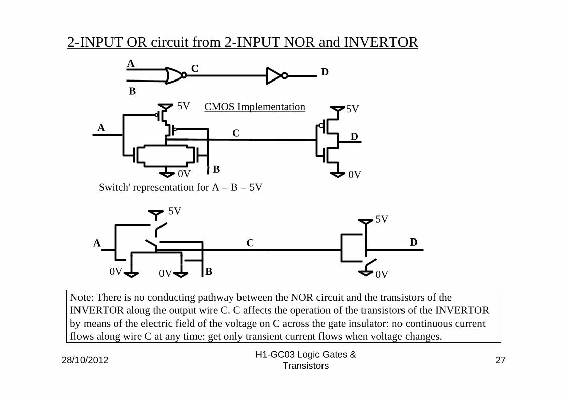
B
A C D
Switch' representation for A = B = 5V
5V5V
0V0V 0V B
C DA
2-INPUT OR circuit from 2-INPUT NOR and INVERTOR
CMOS Implementation5V 5V
0V0V
C DA
B
Note: There is no conducting pathway between the NOR circuit and the transistors of the INVERTOR along the output wire C. C affects the operation of the transistors of the INVERTOR by means of the electric field of the voltage on C across the gate insulator: no continuous current flows along wire C at any time: get only transient current flows when voltage changes.
28/10/2012H1-GC03 Logic Gates &
Transistors28
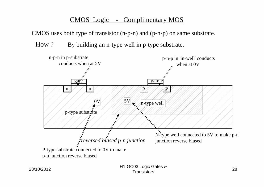
n-type well
p-type substrate
p pnn
n-p-n in p-substrate conducts when at 5V
p-n-p in 'in-well' conducts when at 0V
5V
gategate
0V
reversed biased p-n junction
CMOS Logic - Complimentary MOS
CMOS uses both type of transistor (n-p-n) and (p-n-p) on same substrate.
How ? By building an n-type well in p-type substrate.
N-type well connected to 5V to make p-njunction reverse biased
P-type substrate connected to 0V to make p-n junction reverse biased
28/10/2012H1-GC03 Logic Gates &
Transistors29
Liquid P-typeSilicon
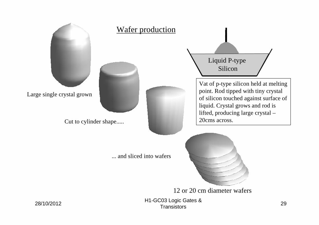
Wafer production
Large single crystal grown
Cut to cylinder shape.....
12 or 20 cm diameter wafers
... and sliced into wafers
Vat of p-type silicon held at melting point. Rod tipped with tiny crystal of silicon touched against surface of liquid. Crystal grows and rod is lifted, producing large crystal –20cms across.
28/10/2012H1-GC03 Logic Gates &
Transistors30
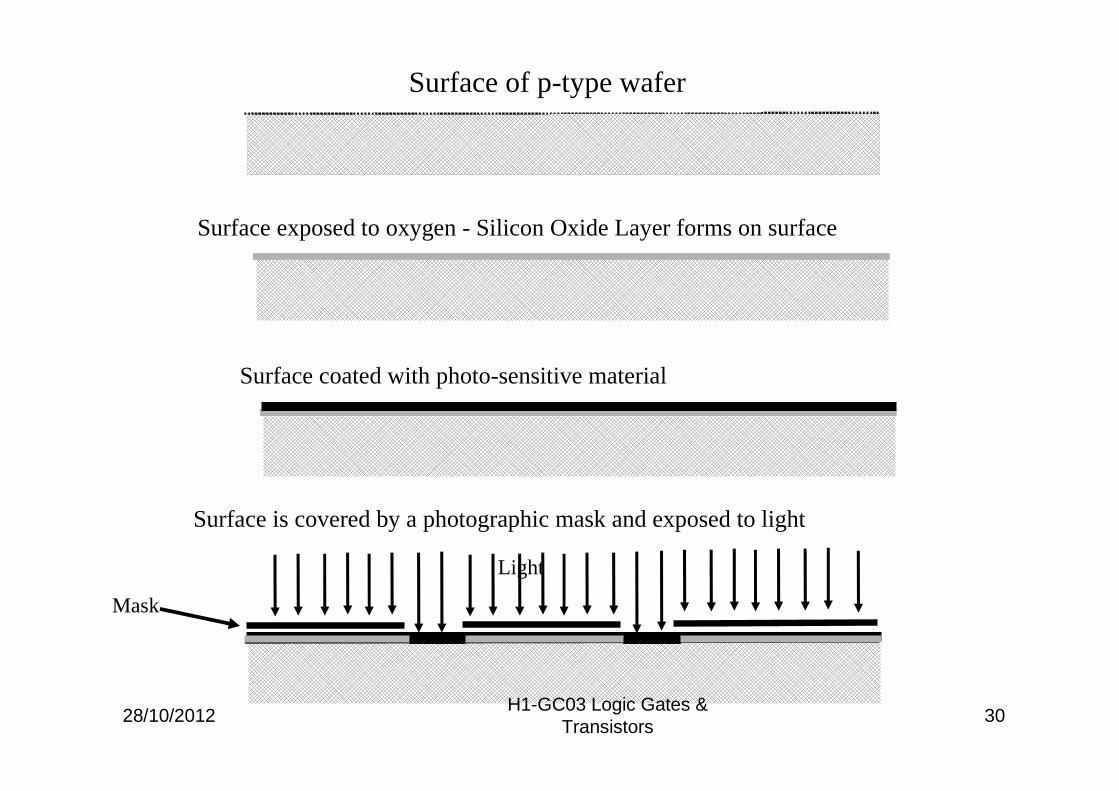
Surface exposed to oxygen - Silicon Oxide Layer forms on surface
Mask
Surface is covered by a photographic mask and exposed to light
Surface coated with photo-sensitive material
Light
Surface of p-type wafer
28/10/2012H1-GC03 Logic Gates &
Transistors31
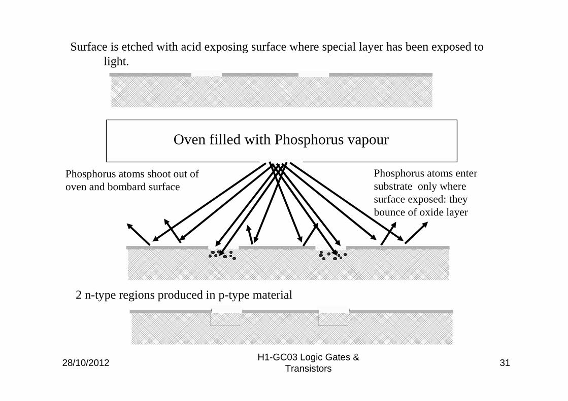
2 n-type regions produced in p-type material
Surface is etched with acid exposing surface where special layer has been exposed to light.
Phosphorus atoms enter substrate only where surface exposed: they bounce of oxide layer
Phosphorus atoms shoot out of oven and bombard surface
Oven filled with Phosphorus vapour
28/10/2012H1-GC03 Logic Gates &
Transistors32
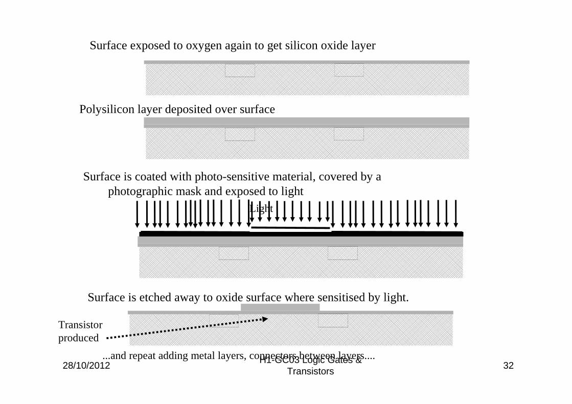
Surface exposed to oxygen again to get silicon oxide layer
Polysilicon layer deposited over surface
Surface is coated with photo-sensitive material, covered by a photographic mask and exposed to light
Light
Surface is etched away to oxide surface where sensitised by light.
Transistor produced
...and repeat adding metal layers, connectors between layers....
28/10/2012H1-GC03 Logic Gates &
Transistors33
28/10/2012H1-GC03 Logic Gates &
Transistors34
28/10/2012H1-GC03 Logic Gates &
Transistors35
28/10/2012H1-GC03 Logic Gates &
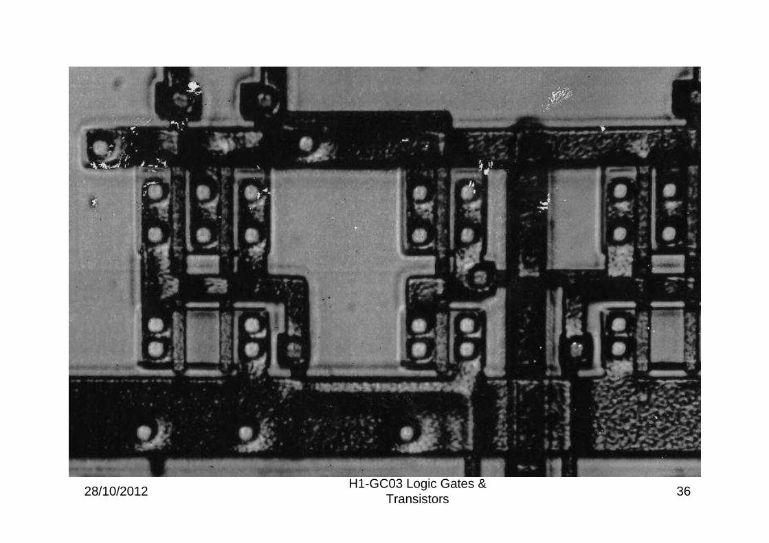
Transistors36
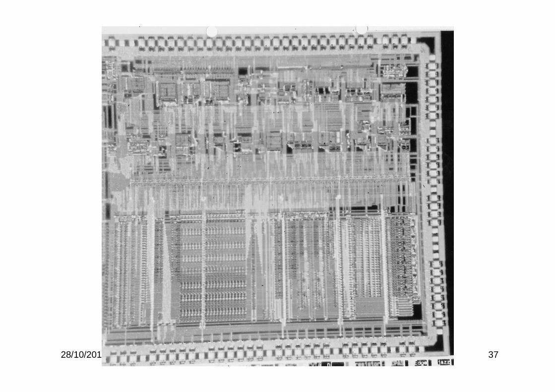
28/10/2012H1-GC03 Logic Gates &
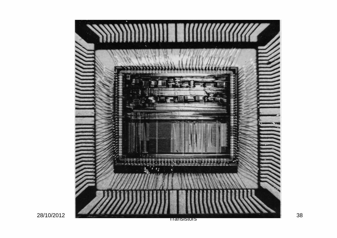
Transistors37
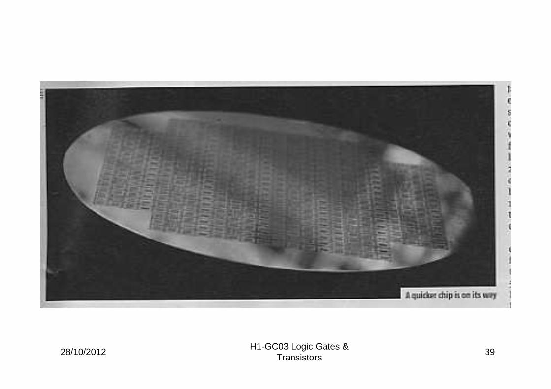
28/10/2012H1-GC03 Logic Gates &
Transistors38
28/10/2012H1-GC03 Logic Gates &
Transistors39
28/10/2012H1-GC03 Logic Gates &
Transistors40


![6HPHVWHU 7LPH WDEOH ZHI -XQH $ 17 · 2020. 6. 25. · 0v /lp /3 0v 1dl +& 0gp :dqj )dqj 55 6fl 1$ 0v (ol]d /rz 0v /lp 6/ 55 (/ 1$ 0v -hqqlihu :x +rph#:: 0u -hiiuh\ &kxd 0v ,y\ 1\dp](https://static.fdocuments.net/doc/165x107/5fd5d0796b0c65670c415668/6hphvwhu-7lph-wdeoh-zhi-xqh-17-2020-6-25-0v-lp-3-0v-1dl-0gp-dqj.jpg)